JP6610648B2 - 撮像装置 - Google Patents
撮像装置 Download PDFInfo
- Publication number
- JP6610648B2 JP6610648B2 JP2017249302A JP2017249302A JP6610648B2 JP 6610648 B2 JP6610648 B2 JP 6610648B2 JP 2017249302 A JP2017249302 A JP 2017249302A JP 2017249302 A JP2017249302 A JP 2017249302A JP 6610648 B2 JP6610648 B2 JP 6610648B2
- Authority
- JP
- Japan
- Prior art keywords
- unit
- imaging
- pixel
- pixel signal
- signal
- Prior art date
- Legal status (The legal status is an assumption and is not a legal conclusion. Google has not performed a legal analysis and makes no representation as to the accuracy of the status listed.)
- Active
Links
Images


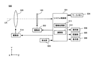


Classifications
-
- H—ELECTRICITY
- H04—ELECTRIC COMMUNICATION TECHNIQUE
- H04N—PICTORIAL COMMUNICATION, e.g. TELEVISION
- H04N25/00—Circuitry of solid-state image sensors [SSIS]; Control thereof
- H04N25/50—Control of the SSIS exposure
- H04N25/53—Control of the integration time
- H04N25/533—Control of the integration time by using differing integration times for different sensor regions
- H04N25/535—Control of the integration time by using differing integration times for different sensor regions by dynamic region selection
Landscapes
- Engineering & Computer Science (AREA)
- Multimedia (AREA)
- Signal Processing (AREA)
- Transforming Light Signals Into Electric Signals (AREA)
- Studio Devices (AREA)
Priority Applications (1)
| Application Number | Priority Date | Filing Date | Title |
|---|---|---|---|
| JP2017249302A JP6610648B2 (ja) | 2017-12-26 | 2017-12-26 | 撮像装置 |
Applications Claiming Priority (1)
| Application Number | Priority Date | Filing Date | Title |
|---|---|---|---|
| JP2017249302A JP6610648B2 (ja) | 2017-12-26 | 2017-12-26 | 撮像装置 |
Related Parent Applications (1)
| Application Number | Title | Priority Date | Filing Date |
|---|---|---|---|
| JP2013053986A Division JP2014179911A (ja) | 2013-03-15 | 2013-03-15 | 撮像装置 |
Publications (3)
| Publication Number | Publication Date |
|---|---|
| JP2018046583A JP2018046583A (ja) | 2018-03-22 |
| JP2018046583A5 JP2018046583A5 (https=) | 2018-09-06 |
| JP6610648B2 true JP6610648B2 (ja) | 2019-11-27 |
Family
ID=61696117
Family Applications (1)
| Application Number | Title | Priority Date | Filing Date |
|---|---|---|---|
| JP2017249302A Active JP6610648B2 (ja) | 2017-12-26 | 2017-12-26 | 撮像装置 |
Country Status (1)
| Country | Link |
|---|---|
| JP (1) | JP6610648B2 (https=) |
Families Citing this family (1)
| Publication number | Priority date | Publication date | Assignee | Title |
|---|---|---|---|---|
| JP2022123970A (ja) * | 2021-02-15 | 2022-08-25 | 株式会社ニコン | 撮像素子、撮像装置、及び半導体モジュール |
Family Cites Families (6)
| Publication number | Priority date | Publication date | Assignee | Title |
|---|---|---|---|---|
| JP3592147B2 (ja) * | 1998-08-20 | 2004-11-24 | キヤノン株式会社 | 固体撮像装置 |
| JP4349232B2 (ja) * | 2004-07-30 | 2009-10-21 | ソニー株式会社 | 半導体モジュール及びmos型固体撮像装置 |
| JP2007150643A (ja) * | 2005-11-28 | 2007-06-14 | Sony Corp | 固体撮像素子、固体撮像素子の駆動方法および撮像装置 |
| JP2010074243A (ja) * | 2008-09-16 | 2010-04-02 | Panasonic Corp | 固体撮像装置、撮像装置 |
| JP5500007B2 (ja) * | 2010-09-03 | 2014-05-21 | ソニー株式会社 | 固体撮像素子およびカメラシステム |
| CN110265415A (zh) * | 2012-03-30 | 2019-09-20 | 株式会社尼康 | 拍摄单元、拍摄装置及拍摄控制程序 |
-
2017
- 2017-12-26 JP JP2017249302A patent/JP6610648B2/ja active Active
Also Published As
| Publication number | Publication date |
|---|---|
| JP2018046583A (ja) | 2018-03-22 |
Similar Documents
| Publication | Publication Date | Title |
|---|---|---|
| JP6780745B2 (ja) | 電子機器 | |
| CN109348148B (zh) | 成像元件及电子设备 | |
| JP2014179911A (ja) | 撮像装置 | |
| JP6413233B2 (ja) | 撮像装置および撮像素子 | |
| JP2014178603A (ja) | 撮像装置 | |
| JP2023052894A (ja) | 撮像素子および撮像装置 | |
| CN105934944B (zh) | 摄像元件及摄像装置 | |
| JP6248468B2 (ja) | 撮像装置および電子機器 | |
| JP2017108281A (ja) | 撮像素子および撮像装置 | |
| JP6488545B2 (ja) | 電子機器 | |
| US12464264B2 (en) | Imaging element and imaging device | |
| JP6056572B2 (ja) | 撮像装置 | |
| JP6610648B2 (ja) | 撮像装置 | |
| JP6349659B2 (ja) | 電子機器、電子機器の制御方法、及び制御プログラム | |
| JP7176583B2 (ja) | 撮像素子および撮像装置 | |
| JP6998693B2 (ja) | 撮像素子及び撮像装置 | |
| JP6179139B2 (ja) | 撮像素子 | |
| JP2018207544A (ja) | 撮像装置および撮像素子 | |
| JP2019083550A (ja) | 電子機器 | |
| JP2017077008A (ja) | 画像処理装置 | |
| JP2023104965A (ja) | 撮像素子および撮像装置 | |
| JP6601465B2 (ja) | 撮像装置 | |
| JP2020115696A (ja) | 撮像素子および撮像装置 | |
| JP2019092220A (ja) | 電子機器 | |
| JP2018029404A (ja) | 撮像素子および撮像装置 |
Legal Events
| Date | Code | Title | Description |
|---|---|---|---|
| A621 | Written request for application examination |
Free format text: JAPANESE INTERMEDIATE CODE: A621 Effective date: 20180125 |
|
| A521 | Request for written amendment filed |
Free format text: JAPANESE INTERMEDIATE CODE: A523 Effective date: 20180725 |
|
| A977 | Report on retrieval |
Free format text: JAPANESE INTERMEDIATE CODE: A971007 Effective date: 20181031 |
|
| A131 | Notification of reasons for refusal |
Free format text: JAPANESE INTERMEDIATE CODE: A131 Effective date: 20181204 |
|
| A601 | Written request for extension of time |
Free format text: JAPANESE INTERMEDIATE CODE: A601 Effective date: 20190201 |
|
| A521 | Request for written amendment filed |
Free format text: JAPANESE INTERMEDIATE CODE: A523 Effective date: 20190402 |
|
| TRDD | Decision of grant or rejection written | ||
| A01 | Written decision to grant a patent or to grant a registration (utility model) |
Free format text: JAPANESE INTERMEDIATE CODE: A01 Effective date: 20191001 |
|
| A61 | First payment of annual fees (during grant procedure) |
Free format text: JAPANESE INTERMEDIATE CODE: A61 Effective date: 20191014 |
|
| R150 | Certificate of patent or registration of utility model |
Ref document number: 6610648 Country of ref document: JP Free format text: JAPANESE INTERMEDIATE CODE: R150 |
|
| R250 | Receipt of annual fees |
Free format text: JAPANESE INTERMEDIATE CODE: R250 |
|
| R250 | Receipt of annual fees |
Free format text: JAPANESE INTERMEDIATE CODE: R250 |
|
| R250 | Receipt of annual fees |
Free format text: JAPANESE INTERMEDIATE CODE: R250 |
|
| R250 | Receipt of annual fees |
Free format text: JAPANESE INTERMEDIATE CODE: R250 |