JP6596817B2 - Light source device and light source device - Google Patents
Light source device and light source device Download PDFInfo
- Publication number
- JP6596817B2 JP6596817B2 JP2014245930A JP2014245930A JP6596817B2 JP 6596817 B2 JP6596817 B2 JP 6596817B2 JP 2014245930 A JP2014245930 A JP 2014245930A JP 2014245930 A JP2014245930 A JP 2014245930A JP 6596817 B2 JP6596817 B2 JP 6596817B2
- Authority
- JP
- Japan
- Prior art keywords
- light emitting
- source device
- light source
- optical
- optical member
- Prior art date
- Legal status (The legal status is an assumption and is not a legal conclusion. Google has not performed a legal analysis and makes no representation as to the accuracy of the status listed.)
- Expired - Fee Related
Links
Images


Description
本発明は、光源デバイス及び光源装置に関する。 The present invention relates to a light source device and a light source apparatus.
2次元の発光素子アレイから射出された光を集光することで高出力レーザーとして用いることが可能であり、特許文献1に開示されているようにレーザー点火プラグの光源として用いられる光源デバイスが知られている。
このような光源デバイスをレーザー点火プラグとして用いるためには、2次元の発光素子アレイからの光を効率良く且つ小スポット状に集光しなければならない。そのためには2次元の発光素子アレイからの放射光を一度コリメートしてから集光することが有効である。
この場合、発光素子ごとにコリメートしなければならないため、コリメートレンズは発光素子に近接した位置に設置しなければならない。このため、2次元のレンズアレイを2次元の発光素子アレイ上に設けることが最も有効である。
The light emitted from the two-dimensional light emitting element array it is possible to use as a high power laser by collecting light, a light source device that is used as a light source of les Za spark plugs as disclosed in Patent Document 1 Is known .
In order to use such a light source device as a laser spark plug, the light from the two-dimensional light emitting element array must be collected efficiently in a small spot shape. For this purpose, it is effective to collimate the radiated light from the two-dimensional light emitting element array once and then collect it.
In this case, since it is necessary to collimate each light emitting element, the collimating lens must be installed at a position close to the light emitting element. For this reason, it is most effective to provide a two-dimensional lens array on the two-dimensional light emitting element array.
2次元の発光素子アレイと2次元のレンズアレイとは高精度な位置合わせが要求され、そのためには2次元の発光素子アレイ上に直接2次元のレンズアレイを半田等により接合して位置がずれないように固定するのがよい。 The two-dimensional light-emitting element array and the two-dimensional lens array are required to be aligned with high precision. For this purpose, the two-dimensional light-emitting element array is directly bonded to the two-dimensional light-emitting element array by soldering or the like, and the position is shifted. It is better to fix so that there is no.
しかしながら、この種の光源デバイスでは、2次元の発光素子アレイと2次元のレンズアレイとの材料が異なり、熱膨張係数が違うため、接合時の残留応力の影響で接合時や経時に接合部にヒビが入ったり剥がれたりするという不具合があった。
接合部にヒビが入ったり剥がれたりすると、2次元の発光素子アレイと2次元のレンズアレイとの位置がずれ、集光効率が低下して出力が低下する。
However, in this type of light source device, the materials of the two-dimensional light-emitting element array and the two-dimensional lens array are different, and the thermal expansion coefficients are different. Therefore, due to the residual stress at the time of bonding, There was a problem of cracks coming in or coming off.
If the joint is cracked or peeled off, the two-dimensional light emitting element array and the two-dimensional lens array are displaced from each other, the light collection efficiency is lowered, and the output is lowered.
本発明は、このような現状に鑑みてなされたもので、接合時の残留応力の発生を抑制でき、長期に亘って高出力を維持できる光源デバイスの提供を、その主な目的とする。 The present invention has been made in view of such a current situation, and a main object thereof is to provide a light source device capable of suppressing the generation of residual stress during bonding and maintaining a high output for a long period of time.
請求項1記載の発明は、複数の発光素子が配列した発光素子アレイを含む発光部材と、前記複数の発光素子から射出される光の光路上にそれぞれ配置される複数の光学素子が配列した光学素子アレイを含み、前記発光部材に対向して配置される光学部材と、前記発光部材と前記光学部材との間における両部材の対向する面に平行な方向の移動及び互いに接近する方向への移動を規制する位置決め部と、前記光学部材と前記発光部材との間に設けられ、前記光学部材と前記発光部材とが離間する方向への移動を規制する保持部とを有し、前記位置決め部は前記光学部材の中央部に位置し、前記保持部は前記光学部材の周辺部に位置し、前記保持部は前記発光部材及び前記光学部材よりも変形し易い材料で形成され、変形により応力を吸収可能であり、前記位置決め部は、前記発光部材及び前記光学部材の少なくとも一方から前記発光部材と前記光学部材との間に突出し球面状の先端を有する凸部と、前記発光部材と前記光学部材の何れか他方に形成され前記凸部に嵌合する円錐状の凹部を含むことを特徴とする。 According to a first aspect of the present invention, there is provided an optical device in which a light emitting member including a light emitting element array in which a plurality of light emitting elements are arranged, and a plurality of optical elements arranged on an optical path of light emitted from the plurality of light emitting elements. It includes element array, wherein an optical member disposed to face the light emitting member, prior SL-emitting member and to the mobile and toward each other in a direction parallel to the opposing surfaces of both members in between the optical member A positioning portion that restricts movement; and a holding portion that is provided between the optical member and the light emitting member and restricts movement in a direction in which the optical member and the light emitting member are separated from each other. Is located in the central part of the optical member, the holding part is located in the peripheral part of the optical member, and the holding part is formed of a material that is easier to deform than the light emitting member and the optical member, Absorbable Ri, the positioning unit includes a projecting portion having a protruding spherical tip between the optical member and the light emitting member from at least one of said light emitting member and the optical member, one of said light emitting member and the optical member It includes a conical recess formed on the other and fitted to the protrusion .
本発明によれば、接合時の残留応力の発生を抑制でき、長期に亘って高出力を維持できる光源デバイスを提供できる。 ADVANTAGE OF THE INVENTION According to this invention, generation | occurrence | production of the residual stress at the time of joining can be suppressed, and the light source device which can maintain a high output over a long term can be provided.
以下、本発明の実施形態を図を参照して説明する。
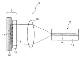
図1乃至図4に基づいて、第1の実施形態を説明する。図1に示すように、本実施形態に係る光学装置2は、光源デバイス4と、光源デバイス4から射出された光を対象物としての光ファイバ6のコア8に集光する集光光学系としての集光レンズ10とを備えている。符号12は、光ファイバ6のクラッドを示している。
光源デバイス4は、複数の発光素子が配列した2次元の発光素子アレイ14を含む発光部材16と、複数の発光素子から射出された光の光路上にそれぞれ配置される複数の光学素子が配列した2次元の光学素子アレイ(以下、「レンズアレイ」という)18を含み、発光部材16に対向して配置される光学部材20とを備えている。
光学装置2は、発光素子アレイ14からの光を効率良くかつ小スポット状に集光し、光ファイバ6に入射させる光学系である。
Embodiments of the present invention will be described below with reference to the drawings.
The first embodiment will be described with reference to FIGS. 1 to 4. As shown in FIG. 1, the
The
The
発光素子アレイ14を出た光は発光素子ごとに放射角を持ったレーザー光であるが、レンズアレイ18を通ることによってコリメートされ、平行光になる。
コリメートされた光は集光レンズ10によってスポット状に集光され、集光された光は光ファイバ6のコア8に入射する。
The light emitted from the light
The collimated light is collected in a spot shape by the
本実施形態に係る光源デバイス4の構成を説明する前に、図17乃至図19に基づいて、従来の光源デバイスの構成について説明する。
図17に示すように、光源デバイス100は、複数の発光素子が配列した2次元の発光素子アレイ102を含む発光部材104と、複数の発光素子から射出された光の光路上にそれぞれ配置される複数の光学素子が配列した2次元のレンズアレイ106を含み、発光部材104に対向して配置される光学部材108とを備えている。
発光素子ごとにコリメートしなければならないため、発光素子アレイ102とレンズアレイ106は、高精度に位置合わせを行っている。
エリア102aは発光素子アレイ102の発光エリアを示し、エリア106aはレンズアレイ106のコリメートエリアを示している。
発光部材104と光学部材108は、固定材(接合材)110により4箇所で固定されている。
Before describing the configuration of the
As shown in FIG. 17, the
Since each light emitting element must be collimated, the light
An
The
しかしながら、発光素子アレイ102とレンズアレイ106との材料が互いに異なり熱膨張係数が違うため、接合時の残留応力の影響で、接合時や経時に接合部にヒビ割れが入ったり剥がれたりするという不具合があった。図18及び図19に基づいてその理由を説明する。
発光素子アレイ102とレンズアレイ106は、一般的に半田などの固定材110で固定される。
このため固定時の温度から常温に戻るときに、熱膨張率の違いから図18に示したようにレンズアレイ106が撓み、固定材110の部分に応力が発生する。
図中矢印の長さは熱による収縮の大きさを示している。
However, since the materials of the light
The light
When returning to normal temperature from the temperature of the was because the solid Ordinary, Les Nzuarei 106 as shown in thermal expansion coefficient difference or al 18 is deflected, stresses occur in the portion of the fixed
The length of the arrow in the figure indicates the magnitude of heat shrinkage.
ここでの発光素子アレイ102はGaAs(ヒ化ガリウム)基板に形成され、レンズアレイ106は石英基板に形成されているため、発光素子アレイ102の方が、収縮が大きくなる。
応力は常に掛かっているため、接合時から常温に戻したときや経時的に固定部分でヒビ割れや破壊が起きる可能性がある。
図19に、そのモードを示している。
図19(a)は発光素子アレイ102の基板にヒビ割れ112aが入った様子を、(b)はレンズアレイ106の基板にヒビ割れ112bが入った様子を、(c)は固定材110にヒビ割れ112cが入った様子をそれぞれ表している。
Here, since the light
Since the stress is always applied, there is a possibility that cracks and breakage may occur in the fixed portion when the temperature is returned to normal temperature from the time of joining or over time.
FIG. 19 shows the mode.
Figure 19 (a) shows how the cracked cracks 112a to the substrate of the light emitting
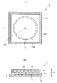
図2乃至図4に基づいて、第1の実施形態に係る光源デバイス4を具体的に説明する。なお、電気的な接合及び発光素子アレイ14と冷却部材との固定は省略してある。
図2に示すように、発光部材16では、発光素子アレイ14が存在する発光エリア14aからレーザー光が射出される。複数の発光素子から射出された光は、レンズアレイ18により発光素子ごとにコリメートされる。
符号18aは発光素子アレイ14からのレーザー光をコリメートするためのレンズが存在するコリメートエリアを示している。
Based on FIG. 2 thru | or FIG. 4, the
As shown in FIG. 2, in the
発光部材16と光学部材20とは、発光部材16と光学部材20との間に設けられ、発光部材16と光学部材20との間における両部材の対向する面に平行な方向(X方向)の移動及び互いに接近する方向(Y方向)への移動を規制する位置決め部22によって固定されている。
位置決め部22は、光学部材20の中央部(ここでは中心)に位置している。
The
The
図3に示すように、一方の部材である光学部材20の中心には、発光部材16側へ向けて突出する凸部22aが一体に形成されている。
図4に示すように、発光部材16の凸部22aに対応する位置には固定部22bが形成されている。
凸部22aと固定部22bとにより位置決め部22が構成され、凸部22aと固定部22bとを半田などの固定材で接合することにより発光部材16と光学部材20とが一体化される。
As shown in FIG. 3, a
As shown in FIG. 4, a fixing
The
このように、発光部材16と光学部材20とを中央部の1箇所で固定することにより、接合時に収縮しても接しているのは中心部の固定部分だけであるので、接合時の熱に起因した収縮差による応力の発生が防止され、接合部である位置決め部22にヒビ割れが入ることは無くなる。
換言すれば、接合時の収縮差による応力を受ける接合部が存在しない。接合時の残留応力が存在しないので、接合時や経時に接合部である位置決め部22にヒビが入ったり剥がれたりするという不具合もない。
位置決め部22における接合自体は従来と変わらない。すなわち、半田などの固定材で接合でき、従来と比べて接合条件を変えなくても安定的な接合ができる。
In this way, by fixing the
In other words, there is no joint that receives stress due to a shrinkage difference during joining. Since there is no residual stress at the time of joining, there is no problem that the
The joining itself in the
位置決め部22の位置は光学部材20の中心に限定されない。発光部材16と光学部材20とを安定的に固定でき、且つ、接合時の残留応力の発生を回避できる光学部材20の中央部と、発光素子アレイ14の領域との間であればよい。
また、凸部22aを他方の部材である発光部材16側に設け、固定部22bを光学部材20側に設ける構成としてもよい。
本実施形態では、位置決め部22を発光部材16又は光学部材20と一体に形成する構成としたが、発光部材16及び光学部材20とは別の部材で形成してもよい(以下の他の実施形態において同じ)。
The position of the
Moreover, it is good also as a structure which provides the
In the present embodiment, the positioning
図5及び図6に第2の実施形態を示す。なお、上記実施形態と同一部分は同一符号で示し、既にした構成上及び機能上の説明は適宜省略する(以下の他の実施形態において同じ)。
基本的な構造は第1の実施形態と同じである。異なる点は、図5に示すように、光学部材20の中心部以外の周辺部と発光部材16との間に、光学部材20と発光部材16とが離間しあるいは接近する方向(Y方向)への移動を規制する変形可能な保持部24が設けられていることである。
本実施形態では、保持部24は、発光エリア14a及びコリメートエリア18aの外側の部分で、光学部材20の4辺の各中央部に配置されている。
保持部24は、発光部材16及び光学部材20よりも変形しやすい材料で形成されている。
5 and 6 show a second embodiment. In addition, the same part as the said embodiment is shown with the same code | symbol, and already demonstrated on the structure and the function are abbreviate | omitted suitably (it is the same in the following other embodiment).
The basic structure is the same as in the first embodiment. The difference is that, as shown in FIG. 5, the
In the present embodiment, the holding
The holding
発光部材16と光学部材20は4箇所で保持部24により接合されているが、接合時の収縮差による応力が発生しても保持部24の変形特性により吸収される。よって、接合部にヒビ割れが入ることはなくなる。
また、振動などが加わっても、変形可能な保持部24で保持しているので、外周部でも大きな変位は生じず、中央部の位置決め部26に大きな力が加わることはなくなる。
本実施形態では中央部と周辺部の計5箇所で支持して固定する構成であるので、発光部材16と光学部材20との初期の位置決め状態を長期に亘って安定的に維持することができる。
The
Further, even if vibration is applied, since it is held by the
In this embodiment, since it is a structure which supports and fixes in a total of five places of a center part and a peripheral part, the initial positioning state of the
図5では、保持部24を光学部材20の4辺の各中央部に配置する構成としたが、図6に示すように、光学部材20の4隅に配置する構成としてもよい。
保持部24の配置箇所は4箇所に限定されずその位置も限定されない。光学部材20の周辺部において、発光部材16との間の固定状態を安定的に維持できる範囲内で2箇所、3箇所、あるいは5箇所以上でもよい。
In FIG. 5, the holding
The arrangement | positioning location of the holding |
図7ないし図9に第3の実施形態を示す。
図7に示すように、本実施形態における位置決め部26は、光学部材20の中央部(ここでは中心)に一体に形成された凸部26aと,発光部材16の凸部26aに対応する位置に形成された凹部26bとから構成されている。図8に示すように、凸部26aの先端は球面状に形成され、図9に示すように、凹部26bは円錐状に形成されている。
第1及び第2の実施形態とは異なり、本実施形態における位置決め部26の凸部26aと凹部26bとは固定されず、単に接触しているだけである。
FIGS. 7 shows a third embodiment in FIG.
As shown in FIG. 7, the positioning
Unlike the first and second embodiments , the
図10に示すように、光学部材20の凸部26aを発光部材16の凹部26bに嵌合すると、凸部26aの球面部が凹部26bの内周面に隙間無く接触し、発光部材16に対する光学部材20の位置決めがなされる。
光学部材20の周辺部と発光部材16との間には、光学部材20と発光部材16とが離間しあるいは接近する方向(Y方向)への移動を規制する変形可能な保持部28が設けられている。
保持部28は、第2の実施形態の保持部24で用いた材料よりも変形しにくい材料、例えばアクリル系の紫外線硬化樹脂を用いている。
中心部の位置決め部26は半田などの固定材で固定しなくてもよいので、保持部28の材料は温度をかけないようなものを選択すれば、それほど変形しやすくなくてもよい。
すなわち、接合時の熱による残留応力を考慮する必要がないので、保持部28には接合時の熱による残留応力を吸収する大きな変形性は要求されない。
As shown in FIG. 10, when the
Between the periphery of the
The holding
Since the
That is, since it is not necessary to consider the residual stress due to heat at the time of joining, the holding
このように中央部の1箇所で位置決めし、周辺部で保持する構成とすることにより、接合時の熱による残留応力の発生を防止できるとともに、発光部材16と光学部材20との初期の位置決め状態を長期に亘って安定的に維持することができる。
Thus, by positioning at one location in the central portion and holding at the peripheral portion, it is possible to prevent the occurrence of residual stress due to heat at the time of joining, and the initial positioning state between the
位置決め部26は、凸部26aを発光部材16側に形成し、凹部26bを光学部材20側に形成する構成としてもよい。
保持部28の配置箇所は、第2の実施形態と同様に図7(a)に示す4箇所及び位置に限定されない。
The
The arrangement | positioning location of the holding |
図11乃至図13に第4の実施形態を示す。
基本的な構造は第3の実施形態と同じである。異なる点は、図11等に示すように、光学部材20の周辺部と発光部材16との間に、発光部材16と光学部材20との間における両部材の対向する面に平行な方向(R方向)の回転及び互いに接近する方向(Y方向)への移動を規制する支持部30が設けられていることである。
支持部30は、光学部材20の周辺部におけるコリメートエリア18aの外側に、位置決め部26とその両側に位置する保持部28とを結んだ線(A―A線)上に位置するように配置されている。
支持部30は、光学部材20に一体に形成された凸部30aと、発光部材16の凸部30aに対応する位置に形成された凹部30bとから構成されている。
図12に示すように、凸部30aの先端は球面状に形成され、図13に示すように、凹部30bは断面V字状に形成されている。
11 to 13 show a fourth embodiment.
The basic structure is the same as in the third embodiment. The difference is that, as shown in FIG. 11 and the like, between the peripheral portion of the
The
The
As shown in FIG. 12, the tip of the
発光部材16と光学部材20は、中央部の位置決め部26と周辺部の支持部30とで位置決めされ、周辺部の保持部28によって保持されている。
位置決め部26と支持部30との組み合わせによって、発光部材16と光学部材20との間が高精度に位置決めされ、支持部30によってR方向の回転も規制されるので、組み付け時の調整もいらなくなり、調整が容易となる。
支持部30は、凸部30aを発光部材16側に形成し、凹部30bを光学部材20側に形成する構成としてもよい。
保持部28の配置箇所は、第2の実施形態と同様に図11(a)に示す4箇所及び位置に限定されない。
The
The combination of the
The
The arrangement | positioning location of the holding |
図14及び図15に第5の実施形態を示す。
基本的な構造は第4の実施形態と同じである。異なる点は、支持部30とは別に、発光部材16と光学部材20との間における両部材の互いに接近する方向(Y方向)への移動を規制する支持部32が設けられていることである。
支持部32は、光学部材20の周辺部であって、コリメート領域18aの外側に配置されている。本実施形態では、A−A線と直交するC−C線上に位置するように配置されている。
発光部材16の支持部32に対応する部位には凹部は設けられていない。支持部32は、位置決め部26及び支持部30と共に、発光部材16と光学部材20間のY方向の位置を規制する部材として機能する。
支持部32は支持部30の凸部30aと同様の形状を有し、その球面状の先端が発光部材16の発光領域14aの外側の表面に接触する。
14 and 15 show a fifth embodiment.
The basic structure is the same as that of the fourth embodiment. A different point is that, apart from the
The
A recess corresponding to the
The
位置決め部26、支持部30及び支持部32の3つの部材で発光部材16と光学部材20間のY方向の位置決めを行うことにより、位置決め精度を高めることができる。
支持部32の位置は上記に限定されない。また、支持部32は発光部材16側に設けてもよい。
By positioning the
The position of the
上記各実施形態では、保持部の材料としてシリコン系接着剤、固定材(接合材)としてAuSn(金錫)を用いている。保持部の材料としては変形可能であればそれ以外の材料でもよい。固定材も半田や有機系接着剤でもよい。
また、上記各実施形態では、位置決め部や支持部を、円錐溝やV字状溝に球面状の凸部を接触させる構成としたが、円柱溝や長穴溝に円柱状の凸部を嵌合させる構成としてもよい。
In each of the above embodiments, a silicon-based adhesive is used as the material of the holding portion, and AuSn (gold tin) is used as the fixing material (joining material). As the material of the holding portion, other materials may be used as long as they can be deformed. The fixing material may also be solder or an organic adhesive.
In each of the above embodiments, the positioning portion and the support portion are configured such that the spherical convex portion is brought into contact with the conical groove or the V-shaped groove, but the cylindrical convex portion is fitted into the cylindrical groove or the long hole groove. It is good also as composition to combine.
図16に光学装置2を用いたレーザー加工機について説明する。
光学装置2の集光レンズ10で集光されたレーザー光が固体レーザー媒質36に入射すると、レーザー光は固体レーザー媒質36で吸収され、固体レーザー媒質36が励起される。
その結果、パルスレーザー光39が出力ミラー40から共振器外部に放射される。符号38は可飽和吸収体を示している。
A laser beam machine using the
When the laser light condensed by the
As a result,
被加工物をテーブルに載置し、テーブルを駆動機構で移動させながら光学装置2からのレーザー光をテーブル上の被加工物に光学系により照射する構成とすることにより、レーザー加工機を構成することができる。
光学装置2と上記光学系とを組み合わせた構成でエンジン等に使用するレーザー点火プラグに用いることもできる。
The laser beam machine is configured by placing the workpiece on the table and irradiating the workpiece on the table with the optical system while moving the table with the driving mechanism. be able to.
It can also be used for a laser spark plug used in an engine or the like in a configuration in which the
以上、本発明の好ましい実施の形態について説明したが、本発明はかかる特定の実施形態に限定されるものではなく、上述の説明で特に限定しない限り、特許請求の範囲に記載された本発明の趣旨の範囲内において、種々の変形・変更が可能である。
本発明の実施の形態に記載された効果は、本発明から生じる最も好適な効果を例示したに過ぎず、本発明による効果は、本発明の実施の形態に記載されたものに限定されるものではない。
The preferred embodiments of the present invention have been described above. However, the present invention is not limited to such specific embodiments, and unless specifically limited by the above description, the present invention described in the claims is not limited. Various modifications and changes are possible within the scope of the gist.
The effects described in the embodiments of the present invention are merely examples of the most preferable effects resulting from the present invention, and the effects of the present invention are limited to those described in the embodiments of the present invention. is not.
4 光源デバイス
6 対象物としての光ファイバ
10 集光光学系としての集光レンズ
14 発光素子アレイ
16 発光部材
18 光学素子アレイ
20 光学部材
24、28 保持部
26 位置決め部
26a 凸部
26b 凹部
30 支持部
30a 凸部
30b 凹部
36 対象物としての固体レーザー媒質
DESCRIPTION OF
Claims (8)
前記複数の発光素子から射出される光の光路上にそれぞれ配置される複数の光学素子が配列した光学素子アレイを含み、前記発光部材に対向して配置される光学部材と、
前記発光部材と前記光学部材との間における両部材の対向する面に平行な方向の移動及び互いに接近する方向への移動を規制する位置決め部と、
前記光学部材と前記発光部材との間に設けられ、前記光学部材と前記発光部材とが離間する方向への移動を規制する保持部と
を有し、
前記位置決め部は前記光学部材の中央部に位置し、前記保持部は前記光学部材の周辺部に位置し、前記保持部は前記発光部材及び前記光学部材よりも変形し易い材料で形成され、変形により応力を吸収可能であり、
前記位置決め部は、前記発光部材及び前記光学部材の少なくとも一方から前記発光部材と前記光学部材との間に突出し球面状の先端を有する凸部と、前記発光部材と前記光学部材の何れか他方に形成され前記凸部に嵌合する円錐状の凹部を含む光源デバイス。 A light emitting member including a light emitting element array in which a plurality of light emitting elements are arranged;
An optical element array including a plurality of optical elements arranged on an optical path of light emitted from the plurality of light emitting elements , the optical member being disposed to face the light emitting member ;
A positioning portion for restricting the movement of the previous SL-emitting member and the direction of movement and approach each other in the direction parallel to the opposing surfaces of both members between the optical member,
A holding portion that is provided between the optical member and the light emitting member and restricts movement in a direction in which the optical member and the light emitting member are separated from each other;
The positioning portion is located in the center of the optical member, the holding portion is located in the peripheral portion of the optical member, and the holding portion is formed of a material that is more easily deformed than the light emitting member and the optical member. absorbable der the stress by is,
The positioning portion includes a convex portion protruding between at least one of the light emitting member and the optical member between the light emitting member and the optical member and having a spherical tip, and one of the light emitting member and the optical member. A light source device including a conical recess formed and fitted to the protrusion .
前記発光部材と前記光学部材とが前記位置決め部で接合されていることを特徴とする光源デバイス。 The light source device according to claim 1.
The light source device, wherein the light emitting member and the optical member are joined at the positioning portion.
前記保持部は前記発光素子アレイ及び前記光学素子アレイの領域の外側に位置することを特徴とする光源デバイス。 The light source device according to claim 1 or 2,
The light source device, wherein the holding unit is located outside a region of the light emitting element array and the optical element array.
前記位置決め部は前記光学部材の中央部と前記発光部材との間に存在することを特徴とする光源デバイス。 The light source device according to any one of claims 1 to 3,
The light source device, wherein the positioning portion exists between a central portion of the optical member and the light emitting member .
前記光学部材の周辺部と前記発光部材との間に、前記発光部材と前記光学部材との間における両部材の対向する面に平行な方向の回転及び互いに接近する方向への移動を規制する支持部が設けられていることを特徴とする光源デバイス。 The light source device according to any one of claims 1 to 4,
A support that regulates rotation between the light emitting member and the optical member in the direction parallel to the opposing surfaces of the light emitting member and the light emitting member and movement in a direction approaching each other between the peripheral portion of the optical member and the light emitting member. A light source device characterized in that a light source device is provided .
前記支持部は前記発光素子アレイ及び前記光学素子アレイの領域の外側に位置することを特徴とする光源デバイス。 The light source device according to claim 5 .
The light source device, wherein the support portion is located outside a region of the light emitting element array and the optical element array .
前記支持部は前記発光部材と前記光学部材の何れか一方に形成された凸部と、他方に形成され前記凸部に嵌合する凹部とを有することを特徴とする光源デバイス。 The light source device according to claim 5 or 6 ,
The light source device, wherein the support portion includes a convex portion formed on one of the light emitting member and the optical member, and a concave portion formed on the other and fitted into the convex portion .
Priority Applications (1)
| Application Number | Priority Date | Filing Date | Title |
|---|---|---|---|
| JP2014245930A JP6596817B2 (en) | 2014-12-04 | 2014-12-04 | Light source device and light source device |
Applications Claiming Priority (1)
| Application Number | Priority Date | Filing Date | Title |
|---|---|---|---|
| JP2014245930A JP6596817B2 (en) | 2014-12-04 | 2014-12-04 | Light source device and light source device |
Publications (3)
| Publication Number | Publication Date |
|---|---|
| JP2016111133A JP2016111133A (en) | 2016-06-20 |
| JP2016111133A5 JP2016111133A5 (en) | 2017-12-07 |
| JP6596817B2 true JP6596817B2 (en) | 2019-10-30 |
Family
ID=56124773
Family Applications (1)
| Application Number | Title | Priority Date | Filing Date |
|---|---|---|---|
| JP2014245930A Expired - Fee Related JP6596817B2 (en) | 2014-12-04 | 2014-12-04 | Light source device and light source device |
Country Status (1)
| Country | Link |
|---|---|
| JP (1) | JP6596817B2 (en) |
Families Citing this family (2)
| Publication number | Priority date | Publication date | Assignee | Title |
|---|---|---|---|---|
| JP6897182B2 (en) * | 2017-03-13 | 2021-06-30 | 株式会社リコー | Light source device and light source device |
| US10914451B2 (en) | 2018-02-07 | 2021-02-09 | Ricoh Company, Ltd. | Optical unit and optical apparatus |
Family Cites Families (21)
| Publication number | Priority date | Publication date | Assignee | Title |
|---|---|---|---|---|
| JPS6247010A (en) * | 1985-08-26 | 1987-02-28 | Konishiroku Photo Ind Co Ltd | Laser scanner |
| US5179609A (en) * | 1991-08-30 | 1993-01-12 | At&T Bell Laboratories | Optical assembly including fiber attachment |
| JP2600298Y2 (en) * | 1992-06-22 | 1999-10-04 | ローム株式会社 | Structure of LED array print head |
| JPH09226167A (en) * | 1996-02-22 | 1997-09-02 | Canon Inc | Manufacture of line light source device, line light source device and image recording device used therefor |
| JPH11307869A (en) * | 1998-04-22 | 1999-11-05 | Furukawa Electric Co Ltd:The | Arrayed optical device module |
| JP2000131583A (en) * | 1998-10-22 | 2000-05-12 | Minolta Co Ltd | Structure for holding optical member |
| JP3824797B2 (en) * | 1999-01-08 | 2006-09-20 | 古河電気工業株式会社 | Light emitting / receiving element module |
| JP4809987B2 (en) * | 2000-03-30 | 2011-11-09 | キヤノン株式会社 | Support structure for optical element, exposure apparatus using the same, and method for manufacturing semiconductor device |
| JP2003202477A (en) * | 2001-12-28 | 2003-07-18 | Sankyo Seiki Mfg Co Ltd | Fixing structure for optical component |
| JP4446149B2 (en) * | 2003-04-10 | 2010-04-07 | ソニー株式会社 | Method for manufacturing composite optical device |
| JP2005276849A (en) * | 2004-02-24 | 2005-10-06 | Ricoh Co Ltd | Led array element, method of manufacturing microlens array thereof optical writing device, and optical reader |
| JP2006269079A (en) * | 2005-03-22 | 2006-10-05 | Hitachi Lighting Ltd | Light source module, liquid crystal display device and manufacturing method for light source module |
| EP1830443B1 (en) * | 2006-03-03 | 2016-06-08 | Fraunhofer USA, Inc. | High power diode laser having multiple emitters and method for its production |
| JP2007311707A (en) * | 2006-05-22 | 2007-11-29 | Ushio Inc | Ultraviolet ray emitting element package |
| JP5131110B2 (en) * | 2008-09-17 | 2013-01-30 | コニカミノルタビジネステクノロジーズ株式会社 | FIXING STRUCTURE, OPTICAL SCANNING DEVICE, IMAGE FORMING DEVICE, AND FIXING METHOD |
| DE102010042453A1 (en) * | 2010-10-14 | 2012-04-19 | Robert Bosch Gmbh | Laser ignition device for an internal combustion engine and operating method thereof |
| JP2012128233A (en) * | 2010-12-16 | 2012-07-05 | Nec Corp | Optical module and mounting method thereof |
| JP5314119B2 (en) * | 2011-12-26 | 2013-10-16 | 株式会社フジクラ | Optical module |
| JP5887950B2 (en) * | 2012-01-23 | 2016-03-16 | ブラザー工業株式会社 | Optical scanning device |
| JP5737254B2 (en) * | 2012-09-26 | 2015-06-17 | 日立金属株式会社 | Optical communication module |
| JP6245629B2 (en) * | 2013-03-26 | 2017-12-13 | 大学共同利用機関法人自然科学研究機構 | In-vehicle ignition system using semiconductor laser pumped solid-state laser device |
-
2014
- 2014-12-04 JP JP2014245930A patent/JP6596817B2/en not_active Expired - Fee Related
Also Published As
| Publication number | Publication date |
|---|---|
| JP2016111133A (en) | 2016-06-20 |
Similar Documents
| Publication | Publication Date | Title |
|---|---|---|
| JP6340902B2 (en) | Manufacturing method of optical module | |
| WO2013168445A1 (en) | Semiconductor laser module | |
| JP6459296B2 (en) | Light emitting module and multi-channel light emitting module | |
| JP5621318B2 (en) | Semiconductor laser module and fiber laser using the same | |
| WO2010047147A1 (en) | Semiconductor laser module and method for manufacturing the same | |
| JP7100236B2 (en) | Wavelength beam coupling device | |
| WO2013150864A1 (en) | Semiconductor laser optical device | |
| WO2011122540A1 (en) | Laser device | |
| JP6596817B2 (en) | Light source device and light source device | |
| US9859679B2 (en) | Semiconductor laser module and method of manufacturing the same | |
| US10686292B2 (en) | Laser module | |
| JP7165337B2 (en) | optical coupler | |
| JP2015075632A (en) | Light source device | |
| KR101574153B1 (en) | Fixed structure of optical component, method of fixing optical component, optical pickup device, and module device with rgb three primary color light source | |
| JP6129066B2 (en) | Semiconductor laser module and manufacturing method thereof | |
| JP4997543B2 (en) | Laser focusing prism | |
| US20180299682A1 (en) | Symmetric Micro-Optic Module | |
| JPWO2020174982A5 (en) | ||
| JP6728641B2 (en) | Light source device | |
| JP2009168846A (en) | Light condensing device and light condensing method | |
| JP2019125726A (en) | Semiconductor laser module and manufacturing method thereof | |
| JP6130427B2 (en) | Laser module | |
| JP6821942B2 (en) | Light source device | |
| JP2009198883A (en) | Light source device | |
| JP6596998B2 (en) | Optical device and light irradiation device |
Legal Events
| Date | Code | Title | Description |
|---|---|---|---|
| A521 | Request for written amendment filed |
Free format text: JAPANESE INTERMEDIATE CODE: A523 Effective date: 20171027 |
|
| A621 | Written request for application examination |
Free format text: JAPANESE INTERMEDIATE CODE: A621 Effective date: 20171027 |
|
| A977 | Report on retrieval |
Free format text: JAPANESE INTERMEDIATE CODE: A971007 Effective date: 20180928 |
|
| A131 | Notification of reasons for refusal |
Free format text: JAPANESE INTERMEDIATE CODE: A131 Effective date: 20181106 |
|
| A521 | Request for written amendment filed |
Free format text: JAPANESE INTERMEDIATE CODE: A523 Effective date: 20190107 |
|
| A131 | Notification of reasons for refusal |
Free format text: JAPANESE INTERMEDIATE CODE: A131 Effective date: 20190618 |
|
| A521 | Request for written amendment filed |
Free format text: JAPANESE INTERMEDIATE CODE: A523 Effective date: 20190819 |
|
| TRDD | Decision of grant or rejection written | ||
| A01 | Written decision to grant a patent or to grant a registration (utility model) |
Free format text: JAPANESE INTERMEDIATE CODE: A01 Effective date: 20190903 |
|
| A61 | First payment of annual fees (during grant procedure) |
Free format text: JAPANESE INTERMEDIATE CODE: A61 Effective date: 20190916 |
|
| R151 | Written notification of patent or utility model registration |
Ref document number: 6596817 Country of ref document: JP Free format text: JAPANESE INTERMEDIATE CODE: R151 |
|
| LAPS | Cancellation because of no payment of annual fees |