US10914451B2 - Optical unit and optical apparatus - Google Patents
Optical unit and optical apparatus Download PDFInfo
- Publication number
- US10914451B2 US10914451B2 US16/256,024 US201916256024A US10914451B2 US 10914451 B2 US10914451 B2 US 10914451B2 US 201916256024 A US201916256024 A US 201916256024A US 10914451 B2 US10914451 B2 US 10914451B2
- Authority
- US
- United States
- Prior art keywords
- optical
- optical module
- light emitting
- emitting element
- optical unit
- Prior art date
- Legal status (The legal status is an assumption and is not a legal conclusion. Google has not performed a legal analysis and makes no representation as to the accuracy of the status listed.)
- Active
Links
- 230000003287 optical effect Effects 0.000 title claims abstract description 211
- 230000017525 heat dissipation Effects 0.000 description 86
- 239000000758 substrate Substances 0.000 description 43
- 230000008602 contraction Effects 0.000 description 20
- 229910000679 solder Inorganic materials 0.000 description 19
- 239000000463 material Substances 0.000 description 18
- 230000035882 stress Effects 0.000 description 15
- 238000000034 method Methods 0.000 description 11
- 239000013307 optical fiber Substances 0.000 description 10
- 239000010949 copper Substances 0.000 description 7
- 229910052802 copper Inorganic materials 0.000 description 6
- 238000010586 diagram Methods 0.000 description 6
- 230000000694 effects Effects 0.000 description 6
- 239000004519 grease Substances 0.000 description 6
- RYGMFSIKBFXOCR-UHFFFAOYSA-N Copper Chemical compound [Cu] RYGMFSIKBFXOCR-UHFFFAOYSA-N 0.000 description 5
- 238000003825 pressing Methods 0.000 description 5
- 230000005284 excitation Effects 0.000 description 4
- 230000008646 thermal stress Effects 0.000 description 4
- 238000005259 measurement Methods 0.000 description 3
- 239000002184 metal Substances 0.000 description 3
- 229910052751 metal Inorganic materials 0.000 description 3
- 239000011347 resin Substances 0.000 description 3
- 229920005989 resin Polymers 0.000 description 3
- 229910000881 Cu alloy Inorganic materials 0.000 description 2
- 239000000919 ceramic Substances 0.000 description 2
- 238000005253 cladding Methods 0.000 description 2
- 238000013461 design Methods 0.000 description 2
- 229910016525 CuMo Inorganic materials 0.000 description 1
- 229910001218 Gallium arsenide Inorganic materials 0.000 description 1
- 229910008433 SnCU Inorganic materials 0.000 description 1
- 239000006096 absorbing agent Substances 0.000 description 1
- 230000007423 decrease Effects 0.000 description 1
- 230000007613 environmental effect Effects 0.000 description 1
- 230000002349 favourable effect Effects 0.000 description 1
- 239000000945 filler Substances 0.000 description 1
- 238000010438 heat treatment Methods 0.000 description 1
- 238000011835 investigation Methods 0.000 description 1
- 238000005461 lubrication Methods 0.000 description 1
- 239000011159 matrix material Substances 0.000 description 1
- 238000012986 modification Methods 0.000 description 1
- 230000004048 modification Effects 0.000 description 1
- 239000002245 particle Substances 0.000 description 1
- 239000010453 quartz Substances 0.000 description 1
- VYPSYNLAJGMNEJ-UHFFFAOYSA-N silicon dioxide Inorganic materials O=[Si]=O VYPSYNLAJGMNEJ-UHFFFAOYSA-N 0.000 description 1
- 229920002379 silicone rubber Polymers 0.000 description 1
- 239000004945 silicone rubber Substances 0.000 description 1
- 229910052709 silver Inorganic materials 0.000 description 1
- 238000012360 testing method Methods 0.000 description 1
- 238000005382 thermal cycling Methods 0.000 description 1
Images


Classifications
-
- F—MECHANICAL ENGINEERING; LIGHTING; HEATING; WEAPONS; BLASTING
- F21—LIGHTING
- F21V—FUNCTIONAL FEATURES OR DETAILS OF LIGHTING DEVICES OR SYSTEMS THEREOF; STRUCTURAL COMBINATIONS OF LIGHTING DEVICES WITH OTHER ARTICLES, NOT OTHERWISE PROVIDED FOR
- F21V5/00—Refractors for light sources
- F21V5/007—Array of lenses or refractors for a cluster of light sources, e.g. for arrangement of multiple light sources in one plane
-
- H—ELECTRICITY
- H01—ELECTRIC ELEMENTS
- H01S—DEVICES USING THE PROCESS OF LIGHT AMPLIFICATION BY STIMULATED EMISSION OF RADIATION [LASER] TO AMPLIFY OR GENERATE LIGHT; DEVICES USING STIMULATED EMISSION OF ELECTROMAGNETIC RADIATION IN WAVE RANGES OTHER THAN OPTICAL
- H01S5/00—Semiconductor lasers
- H01S5/02—Structural details or components not essential to laser action
- H01S5/022—Mountings; Housings
- H01S5/023—Mount members, e.g. sub-mount members
- H01S5/02325—Mechanically integrated components on mount members or optical micro-benches
- H01S5/02326—Arrangements for relative positioning of laser diodes and optical components, e.g. grooves in the mount to fix optical fibres or lenses
-
- F—MECHANICAL ENGINEERING; LIGHTING; HEATING; WEAPONS; BLASTING
- F21—LIGHTING
- F21K—NON-ELECTRIC LIGHT SOURCES USING LUMINESCENCE; LIGHT SOURCES USING ELECTROCHEMILUMINESCENCE; LIGHT SOURCES USING CHARGES OF COMBUSTIBLE MATERIAL; LIGHT SOURCES USING SEMICONDUCTOR DEVICES AS LIGHT-GENERATING ELEMENTS; LIGHT SOURCES NOT OTHERWISE PROVIDED FOR
- F21K9/00—Light sources using semiconductor devices as light-generating elements, e.g. using light-emitting diodes [LED] or lasers
- F21K9/60—Optical arrangements integrated in the light source, e.g. for improving the colour rendering index or the light extraction
-
- G—PHYSICS
- G02—OPTICS
- G02B—OPTICAL ELEMENTS, SYSTEMS OR APPARATUS
- G02B19/00—Condensers, e.g. light collectors or similar non-imaging optics
- G02B19/0004—Condensers, e.g. light collectors or similar non-imaging optics characterised by the optical means employed
- G02B19/0009—Condensers, e.g. light collectors or similar non-imaging optics characterised by the optical means employed having refractive surfaces only
- G02B19/0014—Condensers, e.g. light collectors or similar non-imaging optics characterised by the optical means employed having refractive surfaces only at least one surface having optical power
-
- G—PHYSICS
- G02—OPTICS
- G02B—OPTICAL ELEMENTS, SYSTEMS OR APPARATUS
- G02B27/00—Optical systems or apparatus not provided for by any of the groups G02B1/00 - G02B26/00, G02B30/00
- G02B27/09—Beam shaping, e.g. changing the cross-sectional area, not otherwise provided for
- G02B27/0938—Using specific optical elements
- G02B27/095—Refractive optical elements
- G02B27/0955—Lenses
- G02B27/0961—Lens arrays
-
- G—PHYSICS
- G02—OPTICS
- G02B—OPTICAL ELEMENTS, SYSTEMS OR APPARATUS
- G02B3/00—Simple or compound lenses
- G02B3/0006—Arrays
-
- G—PHYSICS
- G02—OPTICS
- G02B—OPTICAL ELEMENTS, SYSTEMS OR APPARATUS
- G02B7/00—Mountings, adjusting means, or light-tight connections, for optical elements
- G02B7/02—Mountings, adjusting means, or light-tight connections, for optical elements for lenses
- G02B7/021—Mountings, adjusting means, or light-tight connections, for optical elements for lenses for more than one lens
-
- G—PHYSICS
- G02—OPTICS
- G02B—OPTICAL ELEMENTS, SYSTEMS OR APPARATUS
- G02B7/00—Mountings, adjusting means, or light-tight connections, for optical elements
- G02B7/02—Mountings, adjusting means, or light-tight connections, for optical elements for lenses
- G02B7/028—Mountings, adjusting means, or light-tight connections, for optical elements for lenses with means for compensating for changes in temperature or for controlling the temperature; thermal stabilisation
-
- H—ELECTRICITY
- H01—ELECTRIC ELEMENTS
- H01S—DEVICES USING THE PROCESS OF LIGHT AMPLIFICATION BY STIMULATED EMISSION OF RADIATION [LASER] TO AMPLIFY OR GENERATE LIGHT; DEVICES USING STIMULATED EMISSION OF ELECTROMAGNETIC RADIATION IN WAVE RANGES OTHER THAN OPTICAL
- H01S5/00—Semiconductor lasers
-
- H01S5/02252—
-
- H—ELECTRICITY
- H01—ELECTRIC ELEMENTS
- H01S—DEVICES USING THE PROCESS OF LIGHT AMPLIFICATION BY STIMULATED EMISSION OF RADIATION [LASER] TO AMPLIFY OR GENERATE LIGHT; DEVICES USING STIMULATED EMISSION OF ELECTROMAGNETIC RADIATION IN WAVE RANGES OTHER THAN OPTICAL
- H01S5/00—Semiconductor lasers
- H01S5/02—Structural details or components not essential to laser action
- H01S5/024—Arrangements for thermal management
- H01S5/02469—Passive cooling, e.g. where heat is removed by the housing as a whole or by a heat pipe without any active cooling element like a TEC
-
- H—ELECTRICITY
- H01—ELECTRIC ELEMENTS
- H01S—DEVICES USING THE PROCESS OF LIGHT AMPLIFICATION BY STIMULATED EMISSION OF RADIATION [LASER] TO AMPLIFY OR GENERATE LIGHT; DEVICES USING STIMULATED EMISSION OF ELECTROMAGNETIC RADIATION IN WAVE RANGES OTHER THAN OPTICAL
- H01S5/00—Semiconductor lasers
- H01S5/40—Arrangement of two or more semiconductor lasers, not provided for in groups H01S5/02 - H01S5/30
- H01S5/42—Arrays of surface emitting lasers
- H01S5/423—Arrays of surface emitting lasers having a vertical cavity
-
- H04N5/349—
-
- F—MECHANICAL ENGINEERING; LIGHTING; HEATING; WEAPONS; BLASTING
- F21—LIGHTING
- F21Y—INDEXING SCHEME ASSOCIATED WITH SUBCLASSES F21K, F21L, F21S and F21V, RELATING TO THE FORM OR THE KIND OF THE LIGHT SOURCES OR OF THE COLOUR OF THE LIGHT EMITTED
- F21Y2105/00—Planar light sources
- F21Y2105/10—Planar light sources comprising a two-dimensional array of point-like light-generating elements
- F21Y2105/12—Planar light sources comprising a two-dimensional array of point-like light-generating elements characterised by the geometrical disposition of the light-generating elements, e.g. arranging light-generating elements in differing patterns or densities
-
- H—ELECTRICITY
- H01—ELECTRIC ELEMENTS
- H01S—DEVICES USING THE PROCESS OF LIGHT AMPLIFICATION BY STIMULATED EMISSION OF RADIATION [LASER] TO AMPLIFY OR GENERATE LIGHT; DEVICES USING STIMULATED EMISSION OF ELECTROMAGNETIC RADIATION IN WAVE RANGES OTHER THAN OPTICAL
- H01S3/00—Lasers, i.e. devices using stimulated emission of electromagnetic radiation in the infrared, visible or ultraviolet wave range
- H01S3/09—Processes or apparatus for excitation, e.g. pumping
- H01S3/091—Processes or apparatus for excitation, e.g. pumping using optical pumping
- H01S3/094—Processes or apparatus for excitation, e.g. pumping using optical pumping by coherent light
- H01S3/094049—Guiding of the pump light
- H01S3/094053—Fibre coupled pump, e.g. delivering pump light using a fibre or a fibre bundle
-
- H—ELECTRICITY
- H01—ELECTRIC ELEMENTS
- H01S—DEVICES USING THE PROCESS OF LIGHT AMPLIFICATION BY STIMULATED EMISSION OF RADIATION [LASER] TO AMPLIFY OR GENERATE LIGHT; DEVICES USING STIMULATED EMISSION OF ELECTROMAGNETIC RADIATION IN WAVE RANGES OTHER THAN OPTICAL
- H01S3/00—Lasers, i.e. devices using stimulated emission of electromagnetic radiation in the infrared, visible or ultraviolet wave range
- H01S3/09—Processes or apparatus for excitation, e.g. pumping
- H01S3/091—Processes or apparatus for excitation, e.g. pumping using optical pumping
- H01S3/094—Processes or apparatus for excitation, e.g. pumping using optical pumping by coherent light
- H01S3/0941—Processes or apparatus for excitation, e.g. pumping using optical pumping by coherent light of a laser diode
- H01S3/09415—Processes or apparatus for excitation, e.g. pumping using optical pumping by coherent light of a laser diode the pumping beam being parallel to the lasing mode of the pumped medium, e.g. end-pumping
-
- H—ELECTRICITY
- H01—ELECTRIC ELEMENTS
- H01S—DEVICES USING THE PROCESS OF LIGHT AMPLIFICATION BY STIMULATED EMISSION OF RADIATION [LASER] TO AMPLIFY OR GENERATE LIGHT; DEVICES USING STIMULATED EMISSION OF ELECTROMAGNETIC RADIATION IN WAVE RANGES OTHER THAN OPTICAL
- H01S5/00—Semiconductor lasers
- H01S5/005—Optical components external to the laser cavity, specially adapted therefor, e.g. for homogenisation or merging of the beams or for manipulating laser pulses, e.g. pulse shaping
-
- H—ELECTRICITY
- H01—ELECTRIC ELEMENTS
- H01S—DEVICES USING THE PROCESS OF LIGHT AMPLIFICATION BY STIMULATED EMISSION OF RADIATION [LASER] TO AMPLIFY OR GENERATE LIGHT; DEVICES USING STIMULATED EMISSION OF ELECTROMAGNETIC RADIATION IN WAVE RANGES OTHER THAN OPTICAL
- H01S5/00—Semiconductor lasers
- H01S5/02—Structural details or components not essential to laser action
- H01S5/022—Mountings; Housings
- H01S5/02208—Mountings; Housings characterised by the shape of the housings
-
- H—ELECTRICITY
- H01—ELECTRIC ELEMENTS
- H01S—DEVICES USING THE PROCESS OF LIGHT AMPLIFICATION BY STIMULATED EMISSION OF RADIATION [LASER] TO AMPLIFY OR GENERATE LIGHT; DEVICES USING STIMULATED EMISSION OF ELECTROMAGNETIC RADIATION IN WAVE RANGES OTHER THAN OPTICAL
- H01S5/00—Semiconductor lasers
- H01S5/02—Structural details or components not essential to laser action
- H01S5/022—Mountings; Housings
- H01S5/0225—Out-coupling of light
- H01S5/02251—Out-coupling of light using optical fibres
-
- H—ELECTRICITY
- H01—ELECTRIC ELEMENTS
- H01S—DEVICES USING THE PROCESS OF LIGHT AMPLIFICATION BY STIMULATED EMISSION OF RADIATION [LASER] TO AMPLIFY OR GENERATE LIGHT; DEVICES USING STIMULATED EMISSION OF ELECTROMAGNETIC RADIATION IN WAVE RANGES OTHER THAN OPTICAL
- H01S5/00—Semiconductor lasers
- H01S5/02—Structural details or components not essential to laser action
- H01S5/022—Mountings; Housings
- H01S5/0225—Out-coupling of light
- H01S5/02253—Out-coupling of light using lenses
-
- H01S5/02284—
-
- H01S5/02288—
-
- H—ELECTRICITY
- H04—ELECTRIC COMMUNICATION TECHNIQUE
- H04N—PICTORIAL COMMUNICATION, e.g. TELEVISION
- H04N25/00—Circuitry of solid-state image sensors [SSIS]; Control thereof
- H04N25/48—Increasing resolution by shifting the sensor relative to the scene
Definitions
- the disclosures herein generally relate to an optical unit and an optical apparatus.
- Multicolor image forming apparatuses have been recently used for simplified printing as print-on-demand systems, along with an increase in speed.
- high-definition images have been demanded.
- an interval between sub-scanning lines on a photoconductor can be set to 1/n of a recording density and pixels in an n ⁇ m dot matrix configuration can be used.
- the two-dimensional light emitting element array has been used as a light source for a laser ignition plug.
- the two-dimensional light emitting element array is used as an optical component such as a high-power laser, it is desirable to efficiently condense light, emitting from the two-dimensional light emitting element array, into a small spot-like shape. For this purpose, it is effective to collimate light emitted from the two-dimensional light emitting element array before condensing light.
- Patent Document 1 discloses a technique for reducing such residual stress.
- an optical unit includes an optical module that includes a light emitting element array in which a plurality of light emitting elements are arranged, a lens array disposed facing the light emitting element array on an optical path of light emitted from the plurality of light emitting elements, and a fixing part configured to fix the light emitting element array to the lens array.
- the optical unit also includes a member configured to have a larger coefficient of thermal expansion than a coefficient of thermal expansion of the light emitting element array and a fastening part configured to fasten the optical module on a surface of the member.
- the fastening part is configured to fasten the optical module so as to enable expanding and contracting in a plane parallel to the surface of the member.
- Patent Document 1 Japanese Unexamined Patent Application Publication No. 2017-092287
- FIG. 1A is a plan view illustrating an example of a reference optical unit
- FIG. 1B is a cross-sectional view illustrating an example of a reference optical unit
- FIGS. 2A and 2B are plan views illustrating a light emitting device included in the example of a reference optical unit
- FIG. 3 is a diagram illustrating a state in which residual stress occurs in the light emitting device at the time of bonding
- FIGS. 4A through 4C are diagrams illustrating effects of residual stress occurring in the light emitting device
- FIG. 5A is a plan view illustrating an optical unit according to a first embodiment
- FIG. 5B is a cross-sectional view illustrating the optical unit according to the first embodiment
- FIG. 6A is a plan view illustrating an optical unit according to a second embodiment
- FIG. 6B is a cross-sectional view illustrating the optical unit according to the second embodiment
- FIG. 7A is a plan view illustrating an optical unit according to a third embodiment
- FIG. 7B is a cross-sectional view illustrating the optical unit according to the third embodiment.
- FIG. 8A is a plan view illustrating an optical unit according to a fourth embodiment:
- FIG. 8B is a cross-sectional view illustrating the optical unit according to the fourth embodiment.
- FIG. 9A is a plan view illustrating an optical unit according to a fifth embodiment.
- FIG. 9B is a cross-sectional view illustrating the optical unit according to the fifth embodiment.
- FIG. 10 is a diagram illustrating a laser apparatus according to a sixth embodiment.
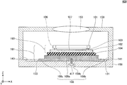
- FIG. 1A is a plan view illustrating an example of a reference optical unit.
- FIG. 1B is a cross-sectional view illustrating an example of the reference optical unit. The cross-sectional view illustrated in FIG. 1B is taken through I-I of FIG. 1A .
- an example of a reference optical unit 900 includes an optical module 961 , a condenser lens 953 , a heat dissipation member 958 , and a cover 959 .
- the optical module 961 includes a light emitting device 960 , a sub-mount 904 , and a package substrate 908 .
- the light emitting device 960 includes a two-dimensional light emitting element array 902 , a two-dimensional lens array 901 , and fixing parts 903 .
- the package substrate 908 includes a base 908 a and flanges 908 b and 908 c that extend from the base 908 a in directions opposite to each other.
- the heat dissipation member 958 has a recess 958 a .
- two positions of the flange 908 b and two positions of the flange 908 c of the optical module 961 are fixed to the heat dissipation member 958 with fixing screws 910 .
- four corners of the package substrate 908 of the optical module 961 are fixed to the heat dissipation member 958 with the fixing screws 910 .
- the condenser lens 953 and the cover 959 are not illustrated.
- FIGS. 2A and 2B are plan views illustrating the light emitting device 960 .
- electrical bonding is not illustrated.
- positions of the light emitting element array 902 and the lens array 901 are adjusted with high accuracy so as to collimate light on a per-light-emitting-element basis.
- An area 907 indicates a light emitting area of the light emitting element array 902
- an area 906 is a collimating area of the lens array 901 .
- the light emitting element array 902 and the lens array 901 are fixed to each other with fixing parts 903 such as solder at four positions.
- FIG. 3 is a diagram illustrating a state in which residual stress occurs in the light emitting device 960 at the time of bonding.
- FIGS. 4A through 4C are diagrams illustrating effects of residual stress occurring in the light emitting device 960 .
- the light emitting element array 902 and the lens array 901 are fixed to each other with the fixing parts 903 such as solder.
- the fixing parts 903 such as solder.
- the lens array 901 may be deformed and stress may be exerted on the fixing parts 903 , as illustrated in FIG. 3 .
- a GaAs substrate is used to form the light emitting element array 902
- a quartz substrate is used to form the lens array 901 .
- the light emitting element array 902 contracts more than the lens array 901 , as illustrated in FIG. 3 .
- Lengths of arrows in FIG. 3 indicate degrees of contraction due to changes in temperature. As stress is always applied, a bonding portion may be cracked or damaged when a heating state is returned to a normal temperature state at the time of bonding, or over time.
- a crack 909 a may occur in the light emitting element array 902 as illustrated in FIG. 4A , for example.
- a crack 909 b may occur in the lens array 901 .
- a crack 909 c may occur in a fixing part 903 .
- Light emitting elements that configure the light emitting element array 902 are of high power and generate a large amount of heat.
- the optical module 961 is fixed to the heat dissipation member 958 in the optical unit 900 .
- the optical module 961 is configured by disposing the light emitting device 960 over the package substrate 908 having a coefficient of thermal expansion similar to that of the light emitting element array 902 , with the sub-mount 904 being interposed therebetween.
- the optical module 961 is fixed to the heat dissipation member 958 , and the optical module 961 is covered by the cover 959 to which the condenser lens 953 is attached.
- a bonding portion may be cracked or peeled off when, in a reliability test, thermal load such as thermal cycling is applied in a state in which the optical module 961 including the light emitting device 960 is fixed to the heat dissipation member 958 .
- thermal load such as thermal cycling is applied in a state in which the optical module 961 including the light emitting device 960 is fixed to the heat dissipation member 958 .
- the inventor has made earnest investigations. As a result, the inventor has found that thermal stress acting on the light emitting element array 902 is significantly larger when the optical module 961 is incorporated into the optical unit 900 than when the optical module 961 is not incorporated into the optical unit 900 and is separated alone.
- the light emitting element array 902 is largely affected by thermal stress of the heat dissipation member 958 and the cover 959 .
- thermal stress of the heat dissipation member 958 and the cover 959 is significantly larger than a coefficient of thermal expansion of the entire optical module 961 , and also because the optical module 961 is fixed to the heat dissipation member 958 .
- design considerations are only for the fixing parts 903 , such large thermal stress is not sufficiently released and the fixing parts 903 may be cracked or peeled off.
- the total volume of the heat dissipation member 958 and the cover 959 is larger than the volume of the optical module 961 .
- the light emitting element array 902 and the lens array 901 are relatively displaced in an optical axis direction or in a direction orthogonal to the optical axis. This causes light such as laser beams emitted from the light emitting elements to fail to pass through proper positions of the lenses. As a result, optical characteristics of the optical unit 900 may deteriorate.
- the heat dissipation member 958 As a material of the heat dissipation member 958 , high-purity copper is preferable in terms of heat dissipation efficiency. However, the coefficient of thermal expansion of copper is large. If high-purity copper is used for the heat dissipation member 958 , coefficients of thermal expansion become largely different between the heat dissipation member 958 and the optical module 961 . In order to reduce such a difference in coefficients of thermal expansion, if copper alloys, ceramics, or the like are used for the heat dissipation member 958 , heat dissipation efficiency significantly decreases, and thus performance of the optical module 961 fails to be sufficiently exhibited. As described above, in the example of the reference optical unit 900 , the performance of the optical module 961 and fracture resistance of the fixing parts 903 are in a trade-off relationship.
- the coefficient of thermal expansion of the lens array 901 is approximately 1 ⁇ 10 ⁇ 6 /° C.
- the coefficient of thermal expansion of the light emitting element array 902 is approximately 6 ⁇ 10 ⁇ 6 /° C.
- the coefficient of thermal expansion of the sub-mount 904 is approximately 7 ⁇ 10 ⁇ 6 /° C.
- the coefficient of thermal expansion of the package substrate 908 is approximately 7 ⁇ 10 ⁇ 6 /° C.
- the coefficient of thermal expansion of the heat dissipation member 958 is approximately 17 ⁇ 10 ⁇ 6 /° C.
- the coefficient of thermal expansion of the cover 959 is approximately 23 ⁇ 10 ⁇ 6 /° C. Therefore, in the example of the reference optical unit 900 , thermal strain becomes significantly large due to influences of the heat dissipation member 958 and the cover 959 .
- FIG. 5A is a plan view illustrating an optical unit according to the first embodiment.
- FIG. 5B is a cross-sectional view illustrating the optical unit according to the first embodiment. The cross-sectional view of FIG. 5B is taken through line I-I of FIG. 5A .
- an optical unit 100 includes an optical module 161 , a condenser lens 153 , a heat dissipation member 158 , and a cover 159 .
- the optical module 161 is fixed to one surface of the heat dissipation member 158 .
- the optical module 161 includes a light emitting device 160 , a sub-mount 104 , and a package substrate 108 .
- the light emitting device 160 includes a two-dimensional light emitting element array 102 , a two-dimensional lens array 101 , and fixing parts 103 .
- the package substrate 108 has a rectangular planar shape, and includes a base 108 a and flanges 108 b and 108 c that extend from the base 108 a in directions opposite to each other.
- the condenser lens 153 and the cover 159 are not illustrated.
- positions of the light emitting element array 102 and the lens array 101 are adjusted with high accuracy so as to collimate light on a per-light-emitting-element basis.
- the light emitting element array 102 and the lens array 101 are bonded to each other with fixing parts 103 such as solder at four positions.
- the light emitting element array 102 includes a two-dimensional light emitting area 107
- the lens array 101 includes a two-dimensional collimating area 106 .
- the light emitting device 160 is bonded to the sub-mount 104 by using solder, for example, and the sub-mount 104 is bonded to the package substrate 108 by using solder, for example.
- the solder used for the fixing parts 103 is Pb-free solder such as SnAgCu-based solder
- the solder used to bond the light emitting element array 102 to the sub-mount 104 is AuSn solder
- the solder used to bond the sub-mount 104 to the package substrate 108 is Pb-free solder such as SnAgCu-based solder.
- the heat dissipation member 158 has a recess 158 a .
- the recess 158 a has a rectangular shape in planar view and has side surfaces 141 through 144 .
- An escape space 115 is formed at a corner where the side surface 141 and the side surface 142 meet.
- a bottom surface, a pair of the side surfaces 141 and 143 , and a pair of the side surfaces 142 and 144 of the recess 158 a are orthogonal to each other.
- the bottom surface is parallel to an XY plane, the side surfaces 141 and 143 are parallel to a YZ plane, and the side surfaces 142 and 144 are parallel to a ZX plane. Accordingly, three orthogonal axes are defined.
- a shape of the optical module 161 in planar view corresponds to a shape of the package substrate 108 in planar view.
- the package substrate 108 has sides 131 through 134 facing the respective side surfaces 141 through 144 .
- the side 131 abuts the side surface 141 that is a first abutting reference surface
- the side 132 abuts the side surface 142 that is a second abutting reference surface.
- a gap is formed between the side 133 and the side surface 143 and between the side 134 and the side surface 144 .
- the abutting reference surfaces are examples of abutting portions.
- the package substrate 108 is fixed to the heat dissipation member 158 with a fixing screw 110 .
- a leaf spring 111 is attached to the heat dissipation member 158 with a fixing screw 112 .
- the fixing screw 110 is an example of a fastening part or a module fixing part.
- the leaf spring 111 and the fixing screw 112 are examples of fastening parts or counteracting parts.
- a pressing force of the leaf spring 111 is 60 N, for example.
- the leaf spring 111 presses a flange 108 c against the bottom surface of the recess 158 a , and also presses the package substrate 108 against the side surface 141 . Therefore, the leaf spring 111 maintains a position in a Z-axis direction of the optical module 161 , while exerting a counteracting force against expansion of the optical module 161 in the XY plane.
- the force exerted from the leaf spring 111 to the optical module 161 maintains the position in the Z-axis direction of the optical module 161 with respect to the dissipation member 158 , but still allows the optical module 161 to expand and contract in the XY plane.
- thermal conductive grease is applied between the package substrate 108 and the heat dissipation member 158 , thus providing thermal conductivity and lubrication between the package substrate 108 and the heat dissipation member 158 .
- light emitted from the light emitting element array 102 is of laser beams having emission angles with respect to each of the light emitting elements.
- the laser beams are collimated when passing through the two-dimensional lens array 101 so as to become collimated light.
- the collimated light is condensed into a spot-like shape by the condenser lens 153 attached to the cover 159 .
- the condensed light is incident on one side of an optical fiber 156 and is emitted from the other side of the optical fiber 156 .
- the optical fiber 156 has a double layer structure having a core 154 located at the center and cladding layers 155 , where the core 154 is confined between the cladding layers 155 .
- the light condensed by the condenser lens 153 is incident on the core 154 and propagates in the core 154 .
- the light emitting element array 102 generates heat when emitting light. Stress exerted on the fixing parts 103 due to a difference in coefficients of thermal expansion between the lens array 101 and the light emitting element array 102 can be reduced by employing the configuration disclosed in Patent Document 1 and providing at least one of the fixing parts 103 with a stress absorbing member. Also, even if a material such as high-purity copper having high heat dissipation efficiency and a large coefficient of thermal expansion is used for the heat dissipation member 158 , the light emitting element array 102 is less affected by thermal strain of the heat dissipation member 158 .
- the optical module 161 and the heat dissipation member 158 are fixed to each other with the fixing screw 110 at only one position, and the leaf spring 111 does not prevent the optical module 161 from expanding and contracting relative to the heat dissipation member 158 while pressing the optical module 161 against the dissipation member 158 . Accordingly, even if the heat dissipation member 158 expands or contracts more than the optical module 161 due to changes in temperature of the light emitting element array 102 , the optical module 161 is less affected by the expansion or contraction of the heat dissipation member 158 . Thus, it becomes possible to prevent a bonding portion from being cracked or peeled off due to the expansion or contraction of the heat dissipation member 158 .
- the optical module 161 thermally expands and thermally contracts, with the position of the fixing screw 110 acting as the origin. Accordingly, even if a thermal expansion and contraction cycle occurs, the position of the optical module 161 with respect to the heat dissipation member 158 is kept constant.
- thermal conductive grease is applied to the lower surface of the package substrate 108 , and the package substrate 108 is placed in the recess 158 a .
- the package substrate 108 is moved in the XY plane, such that the side 131 abuts the side surface 141 , which is the first abutting reference surface, and also the side 132 abuts the side surface 142 , which is the second abutting reference surface.
- a corner where the side 131 and the side 132 of the package substrate 108 meet, enters the escape space 115 and does not make contact with the side surface 141 nor the side surface 142 .
- a flange 108 b is fixed to the heat dissipation member 158 with the fixing screw 110 at only one position.
- a part of the leaf spring 111 is placed on the flange 108 c , so as to maintain a state in which the side 131 makes contact with the side surface 141 , the side 132 makes contact with the side surface 142 , and the lower surface of the optical module 161 makes contact with the bottom surface of the recess 158 a .
- the package substrate 108 can be attached to the heat dissipation member 158 while adjusting the positions with high accuracy.
- FIG. 6A is a plan view illustrating an optical unit according to the second embodiment.
- FIG. 6B is a cross-sectional view illustrating the optical unit according to the second embodiment. The cross-sectional view of FIG. 6B is taken through line I-I of FIG. 6A .
- the condenser lens 153 and the cover 159 are not illustrated.
- the abutting reference surfaces are used as abutting portions in the first embodiment, abutting reference pins are used as abutting portions in the second embodiment.
- two first abutting reference pins 241 are disposed near the side surface 141
- a second abutting reference pin 242 is disposed near the side surface 142 .
- the two abutting reference pins 241 are arranged alongside each other in the Y-axis direction.
- the side 131 of the package substrate 108 abuts the two abutting reference pins 241
- the side 132 of the package substrate 108 abuts the abutting reference pin 242 .
- the leaf spring 111 presses the flange 108 c against the bottom surface of the recess 158 a , and also presses the package substrate 108 against the two abutting reference pins 241 .
- a force exerted from the leaf spring 111 to the optical module 161 maintains the position in the Z-axis direction of the optical module 161 with respect to the dissipation member 158 , but still allows the optical module 161 to expand and contract in the XY plane.
- the escape space 115 is not provided.
- the abutting reference pins 241 and 242 are examples of abutting portions. Other configurations are similar to those of the first embodiment.
- the optical module 161 is less affected by the expansion or contraction of the heat dissipation member 158 .
- the optical module 161 thermally expands and thermally contracts, with the position of the fixing screw 110 acting as the origin. Accordingly, even if a thermal expansion and contraction cycle occurs, the position of the optical module 161 with respect to the heat dissipation member 158 is kept constant.
- thermal conductive grease is applied to the lower surface of the package substrate 108 , and the package substrate 108 is placed in the recess 158 a .
- the package substrate 108 is moved in the XY plane, such that the side 131 abuts the two abutting reference pins 241 , and also the side 132 abuts the abutting reference pin 242 .
- the abutting reference pins 241 are disposed away from the side surface 141 and the abutting reference pin 242 is disposed away from the side surface 142 , a corner where the side 131 and the side 132 of the package substrate 108 meet does not make contact with the side surface 141 nor the side surface 142 . Subsequently, the flange 108 b is fixed to the heat dissipation member 158 with the fixing screw 110 at only one position.
- the package substrate 108 can be attached to the heat dissipation member 158 while adjusting the positions with high accuracy.
- the optical module 161 is positioned by causing the side 131 to abut the side surface 141 , which is the abutting reference surface, or causing the side 132 to abut the side surface 142 , which is the abutting reference surface.
- the escape space 115 may be provided.
- FIG. 7A is a plan view illustrating an optical unit according to the third embodiment.
- FIG. 7B is a cross-sectional view illustrating the optical unit according to the third embodiment. The cross-sectional view of FIG. 7B is taken through line I-I of FIG. 7A .
- the condenser lens 153 and the cover 159 are not illustrated.
- leaf springs 311 a through 311 d and fixing screws 312 a through 312 d are disposed, instead of the fixing screw 110 , the leaf spring 111 , and the fixing screw 112 of the first embodiment. More specifically, within the recess 158 a , in the vicinity of the corner where the side surface 141 and the side surface 142 meet, the leaf spring 311 a is attached to the heat dissipation member 158 with the fixing screw 312 a . Also, in the vicinity of the corner where the side surface 142 and the side surface 143 meet, the leaf spring 311 b is attached to the heat dissipation member 158 with the fixing screw 312 b .
- the leaf spring 311 c is attached to the heat dissipation member 158 with the fixing screw 312 c .
- the leaf spring 311 d is attached to the heat dissipation member 158 with the fixing screw 312 d .
- a part of the leaf spring 311 a and a part of the leaf spring 311 d are placed on the flange 108 b
- a part of the leaf spring 311 b and a part of the leaf spring 311 c are placed on the flange 108 c .
- the leaf springs 311 a and 311 d press the flange 108 b against the bottom surface of the recess 158 a , and also press the package substrate 108 against the leaf springs 311 b and 311 c .
- the leaf springs 311 b and 311 c press the flange 108 c against the bottom surface of the recess 158 a , and also press the package substrate 108 against the leaf springs 311 a and 311 d .
- an elastic member 316 such as silicone rubber is provided between the sides 131 through 134 and the side surfaces 141 through 144 .
- the leaf springs 311 a through 311 d maintain the position in the Z-axis direction of the optical module 161 , while exerting a counteracting force against expansion of the optical module 161 in the XY plane.
- the leaf springs 311 a through 311 d are examples of fastening parts or counteracting parts.
- the elastic member 316 exerts a counteracting force against expansion of the optical module 161 in the XY plane.
- the force exerted from the leaf springs 311 a through 311 d to the optical module 161 maintains the position in the Z-axis direction of the optical module 161 with respect to the dissipation member 158 , but still allows the optical module 161 to expand and contract in the XY plane.
- the escape space 115 is not provided. Other configurations are similar to those of the first embodiment.
- the optical module 161 and the heat dissipation member 158 are not fixed to each other.
- the leaf springs 311 a through 311 d do not prevent expansion and contraction of the heat dissipation member 158 relative to the optical module 161 .
- the optical module 161 is less affected by the expansion or contraction of the heat dissipation member 158 .
- the elastic member 316 in addition to the leaf springs 311 a through 311 d .
- the elastic member 316 By an effect of the elastic member 316 , the optical module 161 elastically deforms in the positive X-direction and the negative X-direction. Accordingly, even if a thermal expansion and contraction cycle occurs, the position of the optical module 161 with respect to the heat dissipation member 158 is kept constant.
- thermal conductive grease is applied to the lower surface of the package substrate 108 , and the package substrate 108 is placed in the recess 158 a .
- the package substrate 108 is moved to a predetermined position in the XY plane.
- a part of the leaf spring 311 a and a part of the leaf spring 311 d are placed on the flange 108 b and a part of the leaf spring 311 c and a part of the leaf spring 311 b are placed on the flange 108 c , such that the leaf springs 311 a and 311 d and leaf springs 311 b and 311 c together press against the optical module 161 , thereby maintaining a state in which the lower surface of the optical module 161 makes contact with the bottom surface of the recess 158 a .
- the package substrate 108 can be attached to the heat dissipation member 158 while adjusting the positions with high accuracy.
- FIG. 8A is a plan view illustrating an optical unit according to the fourth embodiment.
- FIG. 8B is a cross-sectional view illustrating the optical unit according to the fourth embodiment. The cross-sectional view of FIG. 8B is taken through line I-I of FIG. 8A .
- the condenser lens 153 and the cover 159 are not illustrated.
- a center fixing screw 417 is disposed, instead of the fixing screw 110 , the leaf spring 111 , and the fixing screw 112 of the first embodiment. More specifically, a hole 158 b is formed on the lower surface of the heat dissipation member 158 , and the center fixing screw 417 is disposed in the hole 158 b and protrudes from the recess 158 a . Also, the package substrate 108 is fixed to the heat dissipation member 158 with the center fixing screw 417 .
- the center fixing screw 417 is an example of a fastening part or a module fixing part. Also, there is a gap between the sides 131 through 134 and the side surfaces 141 through 144 . Note that the escape space 115 is not provided. Other configurations are similar to those of the first embodiment.
- the optical module 161 and the heat dissipation member 158 are fixed to each other with the center fixing screw 417 at only one position.
- expansion and contraction of the heat dissipation member 158 relative to the optical module 161 is not hindered.
- the optical module 161 is less affected by the expansion or contraction of the heat dissipation member 158 .
- the light emitting element array 102 is less affected by thermal strain of the heat dissipation member 158 .
- the optical module 161 and the heat dissipation member 158 are fixed to each other with the center fixing screw 417 at only one position. Accordingly, even if the heat dissipation member 158 expands or contracts more than the optical module 161 due to changes in temperature of the light emitting element array 102 , the optical module 161 is less affected by the expansion or contraction of the heat dissipation member 158 .
- the optical module 161 thermally expands and thermally contracts, with the position of the screw 417 acting as the origin. Accordingly, even if a thermal expansion and contraction cycle occurs, the position of the optical module 161 with respect to the heat dissipation member 158 is kept constant.
- thermal conductive grease is applied to the lower surface of the package substrate 108 , and the package substrate 108 is placed in the recess 158 a .
- the package substrate 108 is moved to a predetermined position in the X-axis direction and in the Y-axis direction.
- the package substrate 108 is fixed to the heat dissipation member 158 with the center fixing screw 417 at only one position. In this way, the package substrate 108 can be attached to the heat dissipation member 158 while adjusting the positions with high accuracy.
- Thermal conductivity of the center fixing screw 417 is preferably greater than or equal to thermal conductivity of the heat dissipation member 158 .
- a material of the center fixing screw 417 may be the same as the material of the heat dissipation member 158 .
- the material of the center fixing screw 417 is not particularly limited, and is preferably a material having favorable thermal conductivity such as Ag or Cu. Metal such as CuW and CuMo may be used, and ceramics having excellent thermal conductivity such as AlN and SiC may be used.
- FIG. 9A is a plan view illustrating an optical unit according to the fifth embodiment.
- FIG. 9B is a cross-sectional view illustrating the optical unit according to the fifth embodiment. The cross-sectional view of FIG. 9B is taken through line I-I of FIG. 9A .
- the condenser lens 153 and the cover 159 are not illustrated.
- an elastic member 316 is disposed between the package substrate 108 and the side of the recess 158 a of the optical unit 400 according to the fourth embodiment.
- Other configurations are similar to those in the fourth embodiment.
- the optical module 161 is less affected by the expansion or contraction of the heat dissipation member 158 .
- the optical module 161 thermally expands and thermally contracts, with the position of the center fixing screw 417 acting as the origin.
- the elastic member 316 the optical module 161 elastically deforms in the positive X-direction and the negative X-direction. Accordingly, even if a thermal expansion and contraction cycle occurs, the position of the optical module 161 with respect to the heat dissipation member 158 is kept constant.
- a coil spring such as a spring plunger may be used instead of the leaf spring 111 or the leaf spring 311 a through 311 d .
- a pressing force of a leaf spring is not particularly limited, and is preferably 20 N through 200N. If the pressing force is less than 20 N, there may be a possibility that an effect of the leaf spring would not be sufficiently exhibited. If the pressing force exceeds 200 N, there may be a possibility that the optical module 161 would be excessively fastened to the heat dissipation member 158 .
- solder Materials of the solder are not limited to the above-described materials, and SnCu-based solder, SnCuNiP-based solder, or pure Sn solder may be used. Instead of the solder, sintered metal or a resin bonding material having excellent thermal conductivity may be used for bonding. Examples of the sintered metal included sintered Au, sintered Ag, sintered Cu, sintered Ni, and a sintered Cu alloy. Examples of the resin bonding material having excellent thermal conductivity include a resin bonding material containing Au-, Ag-, Cu-, Ni-, or Al-based particles or containing a Au-, Ag-, Cu-, Ni-, or Al-based filler.
- some of the fixing parts 103 are preferably made of a different material from the rest of the fixing parts 103 , or at least one of the fixing parts 103 is provided with a stress absorbing member.
- An elastic member having excellent thermal conductivity may be used, instead of thermal conductive grease applied between the optical module 161 and the heat dissipation member 158 .
- the shape of the optical module in planar view is not limited to a rectangular shape, and may be a circular shape. Regardless of the shape of the optical module in planar view, two counteracting parts such leaf springs are preferably disposed at positions with the centroid of the optical module being interposed therebetween.
- the sixth embodiment relates to a laser apparatus that includes an optical unit.
- the laser apparatus is an example of an optical apparatus.
- FIG. 10 is a diagram illustrating the laser apparatus according to the sixth embodiment.
- a laser apparatus 600 includes a surface-emitting laser array 602 , a first condensing optical system 603 , an optical fiber 604 , a second condensing optical system 605 , and a laser resonator 606 .
- the surface-emitting laser array 602 and the first condensing optical system 603 are included in an optical unit 601 .
- the optical unit 601 the optical unit 100 , 200 , 300 , 400 , or 500 is used, for example.
- the surface-emitting laser array 602 can include the light emitting element array 102
- the first condensing optical system 603 can include the lens array 101 and the condenser lens 153 .
- a direction in which light is emitted from the surface-emitting laser array 602 is regarded as a positive Z-direction.
- the surface-emitting laser array 602 is a light source for excitation and includes a plurality of light emitting parts.
- the light emitting parts are vertical-cavity surface emitting lasers (VCSELs).
- VCSELs vertical-cavity surface emitting lasers
- a wavelength of light emitted from the surface-emitting laser array 602 is 808 nm.
- the surface-emitting laser array 602 In the surface-emitting laser array 602 , a shift in a wavelength of emitted light resulting from temperature is very small. Thus, the surface-emitting laser array 602 is an advantageous light source for excitation by a Q-switched laser in which characteristics largely change due to a shift in an excitation wavelength. Accordingly, when the surface-emitting laser array 602 is used as a light source for excitation, there is an advantage that environmental temperature control becomes easy.
- the first condensing optical system 603 condenses light emitted from the surface-emitting laser array 602 .
- the optical fiber 604 is disposed such that the center of a core on the negative z-side is located at a position where light is condensed by the first condensing optical system 603 .
- an optical fiber having a core diameter of 1.5 mm and a numerical aperture (NA) of 0.39 is used, for example.
- the surface-emitting laser array 602 can be placed away from the laser resonator 606 . Accordingly, flexibility in layout design can be increased.
- Light incident on the optical fiber 604 propagates in the core 154 and is emitted from the positive Z-side of the core.
- the second condensing optical system 605 is disposed on an optical path of light emitted from the optical fiber 604 , and condenses the light.
- the light condensed by the second condensing optical system 605 enters the laser resonator 606 .
- the laser resonator 606 is a Q-switched laser having a laser medium and a saturable absorber, for example. In the laser resonator 606 , light resonates and is amplified.
- the laser resonator 606 is an example of an optical element.
- the optical apparatus is not limited to the laser apparatus.
- the optical apparatus may have a light receiving element as an optical element.
- a measurement object may be irradiated with light, that has been emitted from light emitting elements included in the optical unit 100 , 200 , 300 , 400 , or 500 , and light reflected from or transmitted through the measurement object may enter the light receiving element.
- the optical apparatus may include a configuration in which light, which has been emitted from the light emitting elements included in the optical unit 100 , 200 , 300 , 400 , or 500 , enters the light receiving element through the measurement object.
Landscapes
- Physics & Mathematics (AREA)
- Optics & Photonics (AREA)
- General Physics & Mathematics (AREA)
- Condensed Matter Physics & Semiconductors (AREA)
- Electromagnetism (AREA)
- Engineering & Computer Science (AREA)
- General Engineering & Computer Science (AREA)
- Microelectronics & Electronic Packaging (AREA)
- Multimedia (AREA)
- Signal Processing (AREA)
- Semiconductor Lasers (AREA)
- Optical Couplings Of Light Guides (AREA)
Abstract
Description
Claims (14)
Applications Claiming Priority (4)
| Application Number | Priority Date | Filing Date | Title |
|---|---|---|---|
| JP2018020524 | 2018-02-07 | ||
| JP2018-020524 | 2018-02-07 | ||
| JP2018202108A JP7172445B2 (en) | 2018-02-07 | 2018-10-26 | Optical unit and optical device |
| JP2018-202108 | 2018-10-26 |
Publications (2)
| Publication Number | Publication Date |
|---|---|
| US20190242548A1 US20190242548A1 (en) | 2019-08-08 |
| US10914451B2 true US10914451B2 (en) | 2021-02-09 |
Family
ID=67476007
Family Applications (1)
| Application Number | Title | Priority Date | Filing Date |
|---|---|---|---|
| US16/256,024 Active US10914451B2 (en) | 2018-02-07 | 2019-01-24 | Optical unit and optical apparatus |
Country Status (1)
| Country | Link |
|---|---|
| US (1) | US10914451B2 (en) |
Families Citing this family (1)
| Publication number | Priority date | Publication date | Assignee | Title |
|---|---|---|---|---|
| US11205886B2 (en) * | 2019-03-12 | 2021-12-21 | Nichia Corporation | Method of manufacturing optical member, optical member, and light emitting device |
Citations (11)
| Publication number | Priority date | Publication date | Assignee | Title |
|---|---|---|---|---|
| US20050001896A1 (en) * | 2001-09-28 | 2005-01-06 | Masahide Wakisaka | Resin lens array and optical writing head |
| US20050072981A1 (en) * | 2002-02-19 | 2005-04-07 | Ryoma Suenaga | Light-emitting device and process for producing thereof |
| US20080036103A1 (en) * | 2006-08-09 | 2008-02-14 | Hitachi, Ltd. | Manufacturing method of multi-channel optical module |
| US20090190319A1 (en) | 2008-01-24 | 2009-07-30 | Olympus Corporation | Three-dimensional module |
| US20100201778A1 (en) * | 2006-08-04 | 2010-08-12 | Seiko Epson Corporation | Line Head and an Image Forming Apparatus Using Such a Line Head |
| JP2016111133A (en) | 2014-12-04 | 2016-06-20 | 株式会社リコー | Light source device and light source unit |
| JP2016195330A (en) * | 2015-03-31 | 2016-11-17 | ブラザー工業株式会社 | Print device |
| JP2017092287A (en) | 2015-11-11 | 2017-05-25 | 株式会社リコー | Light source device |
| JP2017204541A (en) | 2016-05-10 | 2017-11-16 | 株式会社リコー | Light source unit and laser unit |
| US20180182928A1 (en) * | 2016-12-27 | 2018-06-28 | Nichia Corporation | Light emitting device |
| JP2018152454A (en) | 2017-03-13 | 2018-09-27 | 株式会社リコー | Light source device and light source apparatus |
-
2019
- 2019-01-24 US US16/256,024 patent/US10914451B2/en active Active
Patent Citations (12)
| Publication number | Priority date | Publication date | Assignee | Title |
|---|---|---|---|---|
| US20050001896A1 (en) * | 2001-09-28 | 2005-01-06 | Masahide Wakisaka | Resin lens array and optical writing head |
| US20050072981A1 (en) * | 2002-02-19 | 2005-04-07 | Ryoma Suenaga | Light-emitting device and process for producing thereof |
| US20100201778A1 (en) * | 2006-08-04 | 2010-08-12 | Seiko Epson Corporation | Line Head and an Image Forming Apparatus Using Such a Line Head |
| US20080036103A1 (en) * | 2006-08-09 | 2008-02-14 | Hitachi, Ltd. | Manufacturing method of multi-channel optical module |
| US20090190319A1 (en) | 2008-01-24 | 2009-07-30 | Olympus Corporation | Three-dimensional module |
| JP2009176947A (en) | 2008-01-24 | 2009-08-06 | Olympus Corp | Three-dimensional module |
| JP2016111133A (en) | 2014-12-04 | 2016-06-20 | 株式会社リコー | Light source device and light source unit |
| JP2016195330A (en) * | 2015-03-31 | 2016-11-17 | ブラザー工業株式会社 | Print device |
| JP2017092287A (en) | 2015-11-11 | 2017-05-25 | 株式会社リコー | Light source device |
| JP2017204541A (en) | 2016-05-10 | 2017-11-16 | 株式会社リコー | Light source unit and laser unit |
| US20180182928A1 (en) * | 2016-12-27 | 2018-06-28 | Nichia Corporation | Light emitting device |
| JP2018152454A (en) | 2017-03-13 | 2018-09-27 | 株式会社リコー | Light source device and light source apparatus |
Also Published As
| Publication number | Publication date |
|---|---|
| US20190242548A1 (en) | 2019-08-08 |
Similar Documents
| Publication | Publication Date | Title |
|---|---|---|
| US5848082A (en) | Low stress heatsink and optical system | |
| JP3909257B2 (en) | Optical coupling device | |
| KR101156815B1 (en) | Optical module | |
| US20120177074A1 (en) | High reliability laser emitter modules | |
| US20100177793A1 (en) | Passive Phase Control in an External Cavity Laser | |
| EP2044663B1 (en) | Misalignment prevention in an external cavity laser having temperature stabilistion of the resonator and the gain medium | |
| WO2016084833A1 (en) | Method for producing optical module | |
| TW200414636A (en) | Laser beam generator and manufacturing method thereof | |
| US10914451B2 (en) | Optical unit and optical apparatus | |
| JP5509317B2 (en) | Laser apparatus and manufacturing method thereof | |
| WO2018142499A1 (en) | Wavelength-variable light source | |
| CN111712975B (en) | Optical module | |
| JP6753478B2 (en) | Optical module | |
| US20040179793A1 (en) | Optoelectronic device packaging assemblies and methods of making the same | |
| JP7172445B2 (en) | Optical unit and optical device | |
| JP5982457B2 (en) | Manufacturing method of optical module | |
| US6970628B2 (en) | Active optical alignment and attachment thereto of a semiconductor optical component with an optical element formed on a planar lightwave circuit | |
| US20180238508A1 (en) | Light source module | |
| US10277003B2 (en) | Laser device and laser device manufacturing method | |
| JP2006072171A (en) | Optical module | |
| CN115280610A (en) | Semiconductor laser device | |
| JP2003158330A (en) | Semiconductor laser coupler | |
| EP2112538B1 (en) | Camera unit | |
| JP2009111065A (en) | Optical semiconductor equipment | |
| CN113620234B (en) | Chip packaging structure, control method and optical computing device |
Legal Events
| Date | Code | Title | Description |
|---|---|---|---|
| AS | Assignment |
Owner name: RICOH COMPANY, LTD., JAPAN Free format text: ASSIGNMENT OF ASSIGNORS INTEREST;ASSIGNOR:HIROI, MASAKI;REEL/FRAME:048120/0077 Effective date: 20190121 |
|
| FEPP | Fee payment procedure |
Free format text: ENTITY STATUS SET TO UNDISCOUNTED (ORIGINAL EVENT CODE: BIG.); ENTITY STATUS OF PATENT OWNER: LARGE ENTITY |
|
| STPP | Information on status: patent application and granting procedure in general |
Free format text: NON FINAL ACTION MAILED |
|
| STPP | Information on status: patent application and granting procedure in general |
Free format text: RESPONSE TO NON-FINAL OFFICE ACTION ENTERED AND FORWARDED TO EXAMINER |
|
| STPP | Information on status: patent application and granting procedure in general |
Free format text: NOTICE OF ALLOWANCE MAILED -- APPLICATION RECEIVED IN OFFICE OF PUBLICATIONS |
|
| STCF | Information on status: patent grant |
Free format text: PATENTED CASE |
|
| MAFP | Maintenance fee payment |
Free format text: PAYMENT OF MAINTENANCE FEE, 4TH YEAR, LARGE ENTITY (ORIGINAL EVENT CODE: M1551); ENTITY STATUS OF PATENT OWNER: LARGE ENTITY Year of fee payment: 4 |