JP6584170B2 - 検出装置、リソグラフィ装置、物品の製造方法、および検出方法 - Google Patents
検出装置、リソグラフィ装置、物品の製造方法、および検出方法 Download PDFInfo
- Publication number
- JP6584170B2 JP6584170B2 JP2015133920A JP2015133920A JP6584170B2 JP 6584170 B2 JP6584170 B2 JP 6584170B2 JP 2015133920 A JP2015133920 A JP 2015133920A JP 2015133920 A JP2015133920 A JP 2015133920A JP 6584170 B2 JP6584170 B2 JP 6584170B2
- Authority
- JP
- Japan
- Prior art keywords
- imaging
- mark
- substrate
- processing unit
- output value
- Prior art date
- Legal status (The legal status is an assumption and is not a legal conclusion. Google has not performed a legal analysis and makes no representation as to the accuracy of the status listed.)
- Active
Links
Images


Classifications
-
- G—PHYSICS
- G03—PHOTOGRAPHY; CINEMATOGRAPHY; ANALOGOUS TECHNIQUES USING WAVES OTHER THAN OPTICAL WAVES; ELECTROGRAPHY; HOLOGRAPHY
- G03F—PHOTOMECHANICAL PRODUCTION OF TEXTURED OR PATTERNED SURFACES, e.g. FOR PRINTING, FOR PROCESSING OF SEMICONDUCTOR DEVICES; MATERIALS THEREFOR; ORIGINALS THEREFOR; APPARATUS SPECIALLY ADAPTED THEREFOR
- G03F7/00—Photomechanical, e.g. photolithographic, production of textured or patterned surfaces, e.g. printing surfaces; Materials therefor, e.g. comprising photoresists; Apparatus specially adapted therefor
- G03F7/70—Microphotolithographic exposure; Apparatus therefor
- G03F7/70691—Handling of masks or workpieces
- G03F7/70775—Position control, e.g. interferometers or encoders for determining the stage position
-
- H—ELECTRICITY
- H01—ELECTRIC ELEMENTS
- H01L—SEMICONDUCTOR DEVICES NOT COVERED BY CLASS H10
- H01L22/00—Testing or measuring during manufacture or treatment; Reliability measurements, i.e. testing of parts without further processing to modify the parts as such; Structural arrangements therefor
- H01L22/10—Measuring as part of the manufacturing process
- H01L22/12—Measuring as part of the manufacturing process for structural parameters, e.g. thickness, line width, refractive index, temperature, warp, bond strength, defects, optical inspection, electrical measurement of structural dimensions, metallurgic measurement of diffusions
-
- G—PHYSICS
- G01—MEASURING; TESTING
- G01N—INVESTIGATING OR ANALYSING MATERIALS BY DETERMINING THEIR CHEMICAL OR PHYSICAL PROPERTIES
- G01N21/00—Investigating or analysing materials by the use of optical means, i.e. using sub-millimetre waves, infrared, visible or ultraviolet light
- G01N21/17—Systems in which incident light is modified in accordance with the properties of the material investigated
- G01N21/1717—Systems in which incident light is modified in accordance with the properties of the material investigated with a modulation of one or more physical properties of the sample during the optical investigation, e.g. electro-reflectance
-
- G—PHYSICS
- G03—PHOTOGRAPHY; CINEMATOGRAPHY; ANALOGOUS TECHNIQUES USING WAVES OTHER THAN OPTICAL WAVES; ELECTROGRAPHY; HOLOGRAPHY
- G03F—PHOTOMECHANICAL PRODUCTION OF TEXTURED OR PATTERNED SURFACES, e.g. FOR PRINTING, FOR PROCESSING OF SEMICONDUCTOR DEVICES; MATERIALS THEREFOR; ORIGINALS THEREFOR; APPARATUS SPECIALLY ADAPTED THEREFOR
- G03F7/00—Photomechanical, e.g. photolithographic, production of textured or patterned surfaces, e.g. printing surfaces; Materials therefor, e.g. comprising photoresists; Apparatus specially adapted therefor
- G03F7/70—Microphotolithographic exposure; Apparatus therefor
- G03F7/70483—Information management; Active and passive control; Testing; Wafer monitoring, e.g. pattern monitoring
- G03F7/70605—Workpiece metrology
- G03F7/70681—Metrology strategies
- G03F7/70683—Mark designs
-
- G—PHYSICS
- G03—PHOTOGRAPHY; CINEMATOGRAPHY; ANALOGOUS TECHNIQUES USING WAVES OTHER THAN OPTICAL WAVES; ELECTROGRAPHY; HOLOGRAPHY
- G03F—PHOTOMECHANICAL PRODUCTION OF TEXTURED OR PATTERNED SURFACES, e.g. FOR PRINTING, FOR PROCESSING OF SEMICONDUCTOR DEVICES; MATERIALS THEREFOR; ORIGINALS THEREFOR; APPARATUS SPECIALLY ADAPTED THEREFOR
- G03F7/00—Photomechanical, e.g. photolithographic, production of textured or patterned surfaces, e.g. printing surfaces; Materials therefor, e.g. comprising photoresists; Apparatus specially adapted therefor
- G03F7/70—Microphotolithographic exposure; Apparatus therefor
- G03F7/70691—Handling of masks or workpieces
- G03F7/70716—Stages
-
- G—PHYSICS
- G03—PHOTOGRAPHY; CINEMATOGRAPHY; ANALOGOUS TECHNIQUES USING WAVES OTHER THAN OPTICAL WAVES; ELECTROGRAPHY; HOLOGRAPHY
- G03F—PHOTOMECHANICAL PRODUCTION OF TEXTURED OR PATTERNED SURFACES, e.g. FOR PRINTING, FOR PROCESSING OF SEMICONDUCTOR DEVICES; MATERIALS THEREFOR; ORIGINALS THEREFOR; APPARATUS SPECIALLY ADAPTED THEREFOR
- G03F7/00—Photomechanical, e.g. photolithographic, production of textured or patterned surfaces, e.g. printing surfaces; Materials therefor, e.g. comprising photoresists; Apparatus specially adapted therefor
- G03F7/70—Microphotolithographic exposure; Apparatus therefor
- G03F7/708—Construction of apparatus, e.g. environment aspects, hygiene aspects or materials
- G03F7/70808—Construction details, e.g. housing, load-lock, seals or windows for passing light in or out of apparatus
- G03F7/70833—Mounting of optical systems, e.g. mounting of illumination system, projection system or stage systems on base-plate or ground
-
- G—PHYSICS
- G03—PHOTOGRAPHY; CINEMATOGRAPHY; ANALOGOUS TECHNIQUES USING WAVES OTHER THAN OPTICAL WAVES; ELECTROGRAPHY; HOLOGRAPHY
- G03F—PHOTOMECHANICAL PRODUCTION OF TEXTURED OR PATTERNED SURFACES, e.g. FOR PRINTING, FOR PROCESSING OF SEMICONDUCTOR DEVICES; MATERIALS THEREFOR; ORIGINALS THEREFOR; APPARATUS SPECIALLY ADAPTED THEREFOR
- G03F9/00—Registration or positioning of originals, masks, frames, photographic sheets or textured or patterned surfaces, e.g. automatically
- G03F9/70—Registration or positioning of originals, masks, frames, photographic sheets or textured or patterned surfaces, e.g. automatically for microlithography
- G03F9/7088—Alignment mark detection, e.g. TTR, TTL, off-axis detection, array detector, video detection
-
- G—PHYSICS
- G06—COMPUTING; CALCULATING OR COUNTING
- G06T—IMAGE DATA PROCESSING OR GENERATION, IN GENERAL
- G06T7/00—Image analysis
- G06T7/0002—Inspection of images, e.g. flaw detection
- G06T7/0004—Industrial image inspection
-
- H—ELECTRICITY
- H01—ELECTRIC ELEMENTS
- H01L—SEMICONDUCTOR DEVICES NOT COVERED BY CLASS H10
- H01L21/00—Processes or apparatus adapted for the manufacture or treatment of semiconductor or solid state devices or of parts thereof
- H01L21/02—Manufacture or treatment of semiconductor devices or of parts thereof
- H01L21/027—Making masks on semiconductor bodies for further photolithographic processing not provided for in group H01L21/18 or H01L21/34
- H01L21/0271—Making masks on semiconductor bodies for further photolithographic processing not provided for in group H01L21/18 or H01L21/34 comprising organic layers
- H01L21/0273—Making masks on semiconductor bodies for further photolithographic processing not provided for in group H01L21/18 or H01L21/34 comprising organic layers characterised by the treatment of photoresist layers
- H01L21/0274—Photolithographic processes
-
- H—ELECTRICITY
- H01—ELECTRIC ELEMENTS
- H01L—SEMICONDUCTOR DEVICES NOT COVERED BY CLASS H10
- H01L21/00—Processes or apparatus adapted for the manufacture or treatment of semiconductor or solid state devices or of parts thereof
- H01L21/67—Apparatus specially adapted for handling semiconductor or electric solid state devices during manufacture or treatment thereof; Apparatus specially adapted for handling wafers during manufacture or treatment of semiconductor or electric solid state devices or components ; Apparatus not specifically provided for elsewhere
- H01L21/67005—Apparatus not specifically provided for elsewhere
- H01L21/67242—Apparatus for monitoring, sorting or marking
- H01L21/67259—Position monitoring, e.g. misposition detection or presence detection
-
- H—ELECTRICITY
- H01—ELECTRIC ELEMENTS
- H01L—SEMICONDUCTOR DEVICES NOT COVERED BY CLASS H10
- H01L22/00—Testing or measuring during manufacture or treatment; Reliability measurements, i.e. testing of parts without further processing to modify the parts as such; Structural arrangements therefor
- H01L22/30—Structural arrangements specially adapted for testing or measuring during manufacture or treatment, or specially adapted for reliability measurements
-
- H—ELECTRICITY
- H01—ELECTRIC ELEMENTS
- H01L—SEMICONDUCTOR DEVICES NOT COVERED BY CLASS H10
- H01L23/00—Details of semiconductor or other solid state devices
- H01L23/544—Marks applied to semiconductor devices or parts, e.g. registration marks, alignment structures, wafer maps
-
- G—PHYSICS
- G01—MEASURING; TESTING
- G01N—INVESTIGATING OR ANALYSING MATERIALS BY DETERMINING THEIR CHEMICAL OR PHYSICAL PROPERTIES
- G01N21/00—Investigating or analysing materials by the use of optical means, i.e. using sub-millimetre waves, infrared, visible or ultraviolet light
- G01N21/17—Systems in which incident light is modified in accordance with the properties of the material investigated
- G01N2021/1765—Method using an image detector and processing of image signal
- G01N2021/177—Detector of the video camera type
-
- G—PHYSICS
- G06—COMPUTING; CALCULATING OR COUNTING
- G06T—IMAGE DATA PROCESSING OR GENERATION, IN GENERAL
- G06T2207/00—Indexing scheme for image analysis or image enhancement
- G06T2207/30—Subject of image; Context of image processing
- G06T2207/30108—Industrial image inspection
- G06T2207/30148—Semiconductor; IC; Wafer
-
- G—PHYSICS
- G06—COMPUTING; CALCULATING OR COUNTING
- G06T—IMAGE DATA PROCESSING OR GENERATION, IN GENERAL
- G06T2207/00—Indexing scheme for image analysis or image enhancement
- G06T2207/30—Subject of image; Context of image processing
- G06T2207/30204—Marker
Description
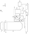
本発明に係る第1実施形態の露光装置100について、図1を参照しながら説明する。図1は、第1実施形態の露光装置100を示す概略図である。露光装置100は、例えば、照明光学系1と、マスク2を保持して移動可能なマスクステージ3と、投影光学系4と、基板5を保持して移動可能な基板ステージ6と、検出部10(検出装置)と、制御部8とを含みうる。制御部8は、例えばCPUやメモリなどを含み、基板5にパターンを形成する処理(マスク2に形成されたパターンを基板5に転写する処理)を制御する。また、制御部8は、基板5にパターンを形成する際の基板ステージ6の位置を、検出部10によって検出された基板上のマーク5aの位置に基づいて制御する。
第1実施形態では、第1撮像における撮像素子12fの出力の第1目標値を、第2撮像における撮像素子12fの出力の第2目標値より小さい値に設定する例について説明した。第2実施形態では、第1撮像における撮像素子12fの出力ゲインを、第2撮像における撮像素子12fの出力ゲインより高い値に設定する例について説明する。第2実施形態では、図8に示すフローチャートにおけるS30の工程が第1実施形態と異なるため、以下では、S30の工程について説明し、その他の工程についての説明を省略する。
本発明の実施形態における物品の製造方法は、例えば、半導体デバイス等のマイクロデバイスや微細構造を有する素子等の物品を製造するのに好適である。本実施形態の物品の製造方法は、基板に塗布された感光剤に上記のリソグラフィ装置(露光装置)を用いて潜像パターンを形成する工程(基板を露光する工程)と、かかる工程で潜像パターンが形成された基板を加工(例えば現像)する工程とを含む。更に、かかる製造方法は、他の周知の工程(酸化、成膜、蒸着、ドーピング、平坦化、エッチング、レジスト剥離、ダイシング、ボンディング、パッケージング等)を含む。本実施形態の物品の製造方法は、従来の方法に比べて、物品の性能・品質・生産性・生産コストの少なくとも1つにおいて有利である。
また、本発明は、以下の処理を実行することによっても実現される。即ち、上述した実施形態の機能を実現するソフトウェア(プログラム)を、ネットワーク又は各種記憶媒体を介してシステム或いは装置に供給し、そのシステム或いは装置のコンピュータ(またはCPUやMPU等)がプログラムを読み出して実行する処理である。
Claims (14)
- 基板上のマークの位置を検出する検出装置であって、
前記マークを撮像する撮像素子を有する撮像部と、
前記撮像部に前記マークを撮像させる第1撮像および前記第1撮像の後の第2撮像を制御し、前記第2撮像によって得られた画像に基づいて前記マークの位置を決定する処理部と、
を含み、
前記処理部は、目標タイミングで前記第2撮像を開始するため、前記撮像素子に蓄積された電荷に応じた出力値が前記第2撮像で用いられる第2目標値より小さい第1目標値になるように決定された第1撮像条件を用いて前記第1撮像を制御し、前記第1撮像条件と前記第1撮像で得られた前記撮像素子の出力値とに基づいて、前記第2撮像において前記撮像素子に蓄積された電荷に応じた出力値が前記第2目標値になるように前記第2撮像で用いられる第2撮像条件を決定する、ことを特徴とする検出装置。 - 前記基板を保持して移動可能なステージを含み、
前記目標タイミングは、前記ステージの振動が許容範囲に収まるタイミングであり、
前記処理部は、前記第2撮像条件が前記目標タイミングまでに決定されるように前記第1撮像を制御する、ことを特徴とする請求項1に記載の検出装置。 - 前記処理部は、前記ステージが目標位置に移動して前記ステージの振動が第1許容範囲に収まったタイミングで前記第1撮像を開始し、その後に前記ステージの振動が前記第1許容範囲より狭い第2許容範囲に収まったタイミングを前記目標タイミングとして前記第2撮像を開始するように前記撮像部を制御する、ことを特徴とする請求項2に記載の検出装置。
- 前記処理部は、前記マークに入射する光の強度と前記第1目標値とに基づいて、前記第1撮像で前記撮像素子に電荷を蓄積させる第1蓄積時間を前記第1撮像条件として決定し、決定された前記第1蓄積時間に基づいて前記第1撮像を制御する、ことを特徴とする請求項1乃至3のうちいずれか1項に記載の検出装置。
- 前記処理部は、前記第1撮像で得られた前記撮像素子の出力値と前記第2目標値との比率を求め、前記比率と前記第1撮像条件とに基づいて前記第2撮像条件を決定する、ことを特徴とする請求項1乃至4のうちいずれか1項に記載の検出装置。
- 前記処理部は、前記第1撮像において前記撮像素子の出力値を増幅するためのゲインを、前記第2撮像において前記撮像素子の出力値を増幅するためのゲインより高い値に設定して前記第1撮像を制御する、ことを特徴とする請求項1乃至5のうちいずれか1項に記載の検出装置。
- 前記第1撮像条件および第2撮像条件はそれぞれ、前記マークに照射される光の強度、前記撮像素子の出力値を増幅するためのゲイン、および前記撮像素子に電荷を蓄積させる蓄積時間のうち少なくとも1つを含む、ことを特徴とする請求項1乃至6のうちいずれか1項に記載の検出装置。
- 基板上のマークの位置を検出する検出装置であって、
前記マークを撮像する撮像素子を有する撮像部と、
前記撮像部に前記マークを撮像させる第1撮像および前記第1撮像の後の第2撮像を制御し、前記第2撮像によって得られた画像に基づいて前記マークの位置を決定する処理部と、
を含み、
前記処理部は、目標タイミングで前記第2撮像を開始するため、前記撮像素子に蓄積された電荷に応じた出力値を増幅するためのゲインを前記第2撮像で用いられる第2ゲインよりも高い第1ゲインに設定した第1撮像条件を用いて前記第1撮像を制御し、前記第1撮像条件と前記第1撮像で得られた前記撮像素子の出力値とに基づいて、前記撮像素子の出力値を増幅するためのゲインを前記第2ゲインに設定した、前記第2撮像で用いられる第2撮像条件を決定する、ことを特徴とする検出装置。 - 前記基板を保持して移動可能なステージを含み、
前記目標タイミングは、前記ステージの振動が許容範囲に収まるタイミングであり、
前記処理部は、前記第2撮像条件が前記目標タイミングまでに決定されるように前記第1撮像を制御する、ことを特徴とする請求項8に記載の検出装置。 - 前記処理部は、前記ステージの振動が前記許容範囲内に収まるタイミングまでに前記第2撮像条件が決定されるように、前記第1撮像に用いられる前記第1撮像条件を決定する、ことを特徴とする請求項2又は9に記載の検出装置。
- 前記処理部は、前記第1撮像の制御における倍率と同じ倍率で前記第2撮像を制御する、ことを特徴とする請求項1乃至10のうちいずれか1項に記載の検出装置。
- 基板にパターンを形成するリソグラフィ装置であって、
前記基板上のマークの位置を検出する請求項1乃至11のうちいずれか1項に記載の検出装置と、
前記基板にパターンを形成する際の前記基板の位置を、前記検出装置によって検出された前記マークの位置に基づいて制御する制御部と、
を含むことを特徴とするリソグラフィ装置。 - 請求項12に記載のリソグラフィ装置を用いて基板にパターンを形成する工程と、
前記工程でパターンの形成を行われた前記基板を加工する工程と、
を含み、加工された前記基板から物品を製造することを特徴とする物品の製造方法。 - 基板上のマークの位置を検出する検出方法であって、
撮像素子によって前記マークの撮像を行う第1撮像工程と、
前記第1撮像工程の後、前記撮像素子によって前記マークの撮像を行う第2撮像工程と、
前記第2撮像工程で得られた画像に基づいて前記マークの位置を決定する決定工程と、
を含み、
前記第1撮像工程は、目標タイミングで前記第2撮像工程を開始するため、前記撮像素子に蓄積された電荷に応じた出力値が前記第2撮像工程で用いられる第2目標値より小さい第1目標値になるように決定された第1撮像条件を用いて前記マークの撮像を行い、前記第1撮像条件と前記第1撮像工程で得られた前記撮像素子の出力値とに基づいて、前記第2撮像工程において前記撮像素子に蓄積された電荷に応じた出力値が前記第2目標値になるように前記第2撮像工程で用いられる第2撮像条件を決定する工程を含む、ことを特徴とする検出方法。
Priority Applications (3)
| Application Number | Priority Date | Filing Date | Title |
|---|---|---|---|
| JP2015133920A JP6584170B2 (ja) | 2015-07-02 | 2015-07-02 | 検出装置、リソグラフィ装置、物品の製造方法、および検出方法 |
| US15/189,043 US10095124B2 (en) | 2015-07-02 | 2016-06-22 | Detection apparatus, lithography apparatus, method of manufacturing article, and detection method |
| KR1020160083252A KR102086409B1 (ko) | 2015-07-02 | 2016-07-01 | 검출 장치, 리소그래피 장치, 물품의 제조 방법, 및 검출 방법 |
Applications Claiming Priority (1)
| Application Number | Priority Date | Filing Date | Title |
|---|---|---|---|
| JP2015133920A JP6584170B2 (ja) | 2015-07-02 | 2015-07-02 | 検出装置、リソグラフィ装置、物品の製造方法、および検出方法 |
Publications (3)
| Publication Number | Publication Date |
|---|---|
| JP2017015994A JP2017015994A (ja) | 2017-01-19 |
| JP2017015994A5 JP2017015994A5 (ja) | 2018-08-09 |
| JP6584170B2 true JP6584170B2 (ja) | 2019-10-02 |
Family
ID=57684431
Family Applications (1)
| Application Number | Title | Priority Date | Filing Date |
|---|---|---|---|
| JP2015133920A Active JP6584170B2 (ja) | 2015-07-02 | 2015-07-02 | 検出装置、リソグラフィ装置、物品の製造方法、および検出方法 |
Country Status (3)
| Country | Link |
|---|---|
| US (1) | US10095124B2 (ja) |
| JP (1) | JP6584170B2 (ja) |
| KR (1) | KR102086409B1 (ja) |
Families Citing this family (3)
| Publication number | Priority date | Publication date | Assignee | Title |
|---|---|---|---|---|
| JP6955344B2 (ja) * | 2017-02-20 | 2021-10-27 | キヤノン株式会社 | インプリント装置、および物品製造方法 |
| DE102018124015B4 (de) * | 2018-09-28 | 2021-07-29 | Basler Ag | System und Verfahren zur Erfassung von Bildern |
| JP2022117091A (ja) * | 2021-01-29 | 2022-08-10 | キヤノン株式会社 | 計測装置、リソグラフィ装置及び物品の製造方法 |
Family Cites Families (16)
| Publication number | Priority date | Publication date | Assignee | Title |
|---|---|---|---|---|
| JP2734004B2 (ja) * | 1988-09-30 | 1998-03-30 | キヤノン株式会社 | 位置合わせ装置 |
| JPH11211415A (ja) * | 1998-01-29 | 1999-08-06 | Canon Inc | 位置検出装置及びそれを用いたデバイスの製造方法 |
| JP2003092248A (ja) * | 2001-09-17 | 2003-03-28 | Canon Inc | 位置検出装置、位置決め装置及びそれらの方法並びに露光装置及びデバイスの製造方法 |
| JP4366031B2 (ja) * | 2001-09-17 | 2009-11-18 | キヤノン株式会社 | 位置検出装置及び方法並びに露光装置、デバイスの製造方法 |
| JP2003092246A (ja) * | 2001-09-17 | 2003-03-28 | Canon Inc | アライメントマーク及びアライメント装置とその方法、及び露光装置、デバイスの製造方法 |
| JP2003203839A (ja) * | 2002-01-04 | 2003-07-18 | Canon Inc | 信号波形補正方法及び被観察面撮像方法並びにそれを用いる露光装置 |
| JP2004006527A (ja) * | 2002-05-31 | 2004-01-08 | Canon Inc | 位置検出装置及び位置検出方法、露光装置、デバイス製造方法並びに基板 |
| JP4102201B2 (ja) | 2003-01-09 | 2008-06-18 | オリンパス株式会社 | 測光装置、電子カメラ |
| JP2004296921A (ja) * | 2003-03-27 | 2004-10-21 | Canon Inc | 位置検出装置 |
| JP4962006B2 (ja) * | 2004-04-23 | 2012-06-27 | 株式会社ニコン | 計測方法、計測装置、露光方法及び露光装置 |
| JP4307482B2 (ja) * | 2006-12-19 | 2009-08-05 | キヤノン株式会社 | 位置計測装置、露光装置、およびデバイス製造方法 |
| EP2131245A3 (en) * | 2008-06-02 | 2012-08-01 | ASML Netherlands BV | Lithographic apparatus and its focus determination method |
| JP2009300798A (ja) * | 2008-06-13 | 2009-12-24 | Canon Inc | 露光装置およびデバイス製造方法 |
| JP5550253B2 (ja) * | 2009-04-22 | 2014-07-16 | キヤノン株式会社 | マーク位置検出装置及びマーク位置検出方法、それを用いた露光装置及びデバイスの製造方法 |
| JP2013145871A (ja) * | 2011-12-13 | 2013-07-25 | Canon Inc | リソグラフィー装置および方法、ならびに物品製造方法 |
| JP6213912B2 (ja) * | 2013-05-02 | 2017-10-18 | 株式会社タムロン | 小型高変倍ズームレンズ |
-
2015
- 2015-07-02 JP JP2015133920A patent/JP6584170B2/ja active Active
-
2016
- 2016-06-22 US US15/189,043 patent/US10095124B2/en active Active
- 2016-07-01 KR KR1020160083252A patent/KR102086409B1/ko active IP Right Grant
Also Published As
| Publication number | Publication date |
|---|---|
| US10095124B2 (en) | 2018-10-09 |
| US20170005017A1 (en) | 2017-01-05 |
| JP2017015994A (ja) | 2017-01-19 |
| KR102086409B1 (ko) | 2020-03-09 |
| KR20170004889A (ko) | 2017-01-11 |
Similar Documents
| Publication | Publication Date | Title |
|---|---|---|
| TWI620994B (zh) | 在疊對精密測定中用於對比增強的結構照明 | |
| JP6463935B2 (ja) | 露光装置、露光方法、およびデバイス製造方法 | |
| JP6584170B2 (ja) | 検出装置、リソグラフィ装置、物品の製造方法、および検出方法 | |
| US8339570B2 (en) | Mark position detection device and mark position detection method, exposure apparatus using same, and device manufacturing method | |
| JP2017032369A (ja) | パターン検査装置及びパターン検査方法 | |
| JP2004022797A (ja) | マーク位置検出装置およびマーク位置検出方法 | |
| KR102242152B1 (ko) | 리소그래피 장치 및 물품 제조 방법 | |
| US20190146359A1 (en) | Exposure apparatus and method of manufacturing article | |
| KR101895834B1 (ko) | 검출장치, 계측장치, 노광장치, 물품의 제조방법, 및 계측방법 | |
| KR102554833B1 (ko) | 오버레이 계측 장치 및 오버레이 계측 방법 | |
| JP6661303B2 (ja) | 位置検出装置、位置検出方法、露光装置及び露光方法 | |
| WO2018051744A1 (ja) | 検出装置、検出方法、パターニング装置、および物品の製造方法 | |
| JP7397096B2 (ja) | 結像デバイス向けの自動焦点方法 | |
| JPH11288867A (ja) | 位置合わせ方法、アライメントマークの形成方法、露光装置及び露光方法 | |
| JP7198731B2 (ja) | 撮像装置、及びフォーカス調整方法 | |
| JP4710068B2 (ja) | 焦点調整機構、検査装置及び焦点調整方法 | |
| JP2006071440A (ja) | 位置計測装置、該位置計測装置を備えた露光装置及び該位置計測装置を使用する露光方法 | |
| JP2004102064A (ja) | 画像測定装置 | |
| JP2000216077A (ja) | 重ね合わせ精度測定装置の焦点位置調整方法及び調整装置 | |
| JP2002237452A (ja) | 投影露光方法及び装置、デバイス製造方法、並びに該方法により製造されたデバイス |
Legal Events
| Date | Code | Title | Description |
|---|---|---|---|
| A521 | Written amendment |
Free format text: JAPANESE INTERMEDIATE CODE: A523 Effective date: 20180627 |
|
| A621 | Written request for application examination |
Free format text: JAPANESE INTERMEDIATE CODE: A621 Effective date: 20180627 |
|
| A977 | Report on retrieval |
Free format text: JAPANESE INTERMEDIATE CODE: A971007 Effective date: 20190510 |
|
| A131 | Notification of reasons for refusal |
Free format text: JAPANESE INTERMEDIATE CODE: A131 Effective date: 20190520 |
|
| A521 | Written amendment |
Free format text: JAPANESE INTERMEDIATE CODE: A523 Effective date: 20190718 |
|
| TRDD | Decision of grant or rejection written | ||
| A01 | Written decision to grant a patent or to grant a registration (utility model) |
Free format text: JAPANESE INTERMEDIATE CODE: A01 Effective date: 20190805 |
|
| A61 | First payment of annual fees (during grant procedure) |
Free format text: JAPANESE INTERMEDIATE CODE: A61 Effective date: 20190903 |
|
| R151 | Written notification of patent or utility model registration |
Ref document number: 6584170 Country of ref document: JP Free format text: JAPANESE INTERMEDIATE CODE: R151 |