JP6572095B2 - 表示装置 - Google Patents
表示装置 Download PDFInfo
- Publication number
- JP6572095B2 JP6572095B2 JP2015212091A JP2015212091A JP6572095B2 JP 6572095 B2 JP6572095 B2 JP 6572095B2 JP 2015212091 A JP2015212091 A JP 2015212091A JP 2015212091 A JP2015212091 A JP 2015212091A JP 6572095 B2 JP6572095 B2 JP 6572095B2
- Authority
- JP
- Japan
- Prior art keywords
- display
- signal
- potential
- period
- pixel electrode
- Prior art date
- Legal status (The legal status is an assumption and is not a legal conclusion. Google has not performed a legal analysis and makes no representation as to the accuracy of the status listed.)
- Active
Links
Images


Classifications
-
- G—PHYSICS
- G09—EDUCATION; CRYPTOGRAPHY; DISPLAY; ADVERTISING; SEALS
- G09G—ARRANGEMENTS OR CIRCUITS FOR CONTROL OF INDICATING DEVICES USING STATIC MEANS TO PRESENT VARIABLE INFORMATION
- G09G3/00—Control arrangements or circuits, of interest only in connection with visual indicators other than cathode-ray tubes
- G09G3/20—Control arrangements or circuits, of interest only in connection with visual indicators other than cathode-ray tubes for presentation of an assembly of a number of characters, e.g. a page, by composing the assembly by combination of individual elements arranged in a matrix no fixed position being assigned to or needed to be assigned to the individual characters or partial characters
- G09G3/34—Control arrangements or circuits, of interest only in connection with visual indicators other than cathode-ray tubes for presentation of an assembly of a number of characters, e.g. a page, by composing the assembly by combination of individual elements arranged in a matrix no fixed position being assigned to or needed to be assigned to the individual characters or partial characters by control of light from an independent source
- G09G3/36—Control arrangements or circuits, of interest only in connection with visual indicators other than cathode-ray tubes for presentation of an assembly of a number of characters, e.g. a page, by composing the assembly by combination of individual elements arranged in a matrix no fixed position being assigned to or needed to be assigned to the individual characters or partial characters by control of light from an independent source using liquid crystals
- G09G3/3611—Control of matrices with row and column drivers
- G09G3/3614—Control of polarity reversal in general
-
- G—PHYSICS
- G09—EDUCATION; CRYPTOGRAPHY; DISPLAY; ADVERTISING; SEALS
- G09G—ARRANGEMENTS OR CIRCUITS FOR CONTROL OF INDICATING DEVICES USING STATIC MEANS TO PRESENT VARIABLE INFORMATION
- G09G3/00—Control arrangements or circuits, of interest only in connection with visual indicators other than cathode-ray tubes
- G09G3/20—Control arrangements or circuits, of interest only in connection with visual indicators other than cathode-ray tubes for presentation of an assembly of a number of characters, e.g. a page, by composing the assembly by combination of individual elements arranged in a matrix no fixed position being assigned to or needed to be assigned to the individual characters or partial characters
- G09G3/34—Control arrangements or circuits, of interest only in connection with visual indicators other than cathode-ray tubes for presentation of an assembly of a number of characters, e.g. a page, by composing the assembly by combination of individual elements arranged in a matrix no fixed position being assigned to or needed to be assigned to the individual characters or partial characters by control of light from an independent source
- G09G3/36—Control arrangements or circuits, of interest only in connection with visual indicators other than cathode-ray tubes for presentation of an assembly of a number of characters, e.g. a page, by composing the assembly by combination of individual elements arranged in a matrix no fixed position being assigned to or needed to be assigned to the individual characters or partial characters by control of light from an independent source using liquid crystals
- G09G3/3611—Control of matrices with row and column drivers
- G09G3/3674—Details of drivers for scan electrodes
- G09G3/3677—Details of drivers for scan electrodes suitable for active matrices only
-
- G—PHYSICS
- G02—OPTICS
- G02F—OPTICAL DEVICES OR ARRANGEMENTS FOR THE CONTROL OF LIGHT BY MODIFICATION OF THE OPTICAL PROPERTIES OF THE MEDIA OF THE ELEMENTS INVOLVED THEREIN; NON-LINEAR OPTICS; FREQUENCY-CHANGING OF LIGHT; OPTICAL LOGIC ELEMENTS; OPTICAL ANALOGUE/DIGITAL CONVERTERS
- G02F1/00—Devices or arrangements for the control of the intensity, colour, phase, polarisation or direction of light arriving from an independent light source, e.g. switching, gating or modulating; Non-linear optics
- G02F1/01—Devices or arrangements for the control of the intensity, colour, phase, polarisation or direction of light arriving from an independent light source, e.g. switching, gating or modulating; Non-linear optics for the control of the intensity, phase, polarisation or colour
- G02F1/13—Devices or arrangements for the control of the intensity, colour, phase, polarisation or direction of light arriving from an independent light source, e.g. switching, gating or modulating; Non-linear optics for the control of the intensity, phase, polarisation or colour based on liquid crystals, e.g. single liquid crystal display cells
- G02F1/133—Constructional arrangements; Operation of liquid crystal cells; Circuit arrangements
- G02F1/136—Liquid crystal cells structurally associated with a semi-conducting layer or substrate, e.g. cells forming part of an integrated circuit
- G02F1/1362—Active matrix addressed cells
- G02F1/13624—Active matrix addressed cells having more than one switching element per pixel
-
- G—PHYSICS
- G02—OPTICS
- G02F—OPTICAL DEVICES OR ARRANGEMENTS FOR THE CONTROL OF LIGHT BY MODIFICATION OF THE OPTICAL PROPERTIES OF THE MEDIA OF THE ELEMENTS INVOLVED THEREIN; NON-LINEAR OPTICS; FREQUENCY-CHANGING OF LIGHT; OPTICAL LOGIC ELEMENTS; OPTICAL ANALOGUE/DIGITAL CONVERTERS
- G02F1/00—Devices or arrangements for the control of the intensity, colour, phase, polarisation or direction of light arriving from an independent light source, e.g. switching, gating or modulating; Non-linear optics
- G02F1/01—Devices or arrangements for the control of the intensity, colour, phase, polarisation or direction of light arriving from an independent light source, e.g. switching, gating or modulating; Non-linear optics for the control of the intensity, phase, polarisation or colour
- G02F1/13—Devices or arrangements for the control of the intensity, colour, phase, polarisation or direction of light arriving from an independent light source, e.g. switching, gating or modulating; Non-linear optics for the control of the intensity, phase, polarisation or colour based on liquid crystals, e.g. single liquid crystal display cells
- G02F1/133—Constructional arrangements; Operation of liquid crystal cells; Circuit arrangements
- G02F1/13306—Circuit arrangements or driving methods for the control of single liquid crystal cells
-
- G—PHYSICS
- G02—OPTICS
- G02F—OPTICAL DEVICES OR ARRANGEMENTS FOR THE CONTROL OF LIGHT BY MODIFICATION OF THE OPTICAL PROPERTIES OF THE MEDIA OF THE ELEMENTS INVOLVED THEREIN; NON-LINEAR OPTICS; FREQUENCY-CHANGING OF LIGHT; OPTICAL LOGIC ELEMENTS; OPTICAL ANALOGUE/DIGITAL CONVERTERS
- G02F1/00—Devices or arrangements for the control of the intensity, colour, phase, polarisation or direction of light arriving from an independent light source, e.g. switching, gating or modulating; Non-linear optics
- G02F1/01—Devices or arrangements for the control of the intensity, colour, phase, polarisation or direction of light arriving from an independent light source, e.g. switching, gating or modulating; Non-linear optics for the control of the intensity, phase, polarisation or colour
- G02F1/13—Devices or arrangements for the control of the intensity, colour, phase, polarisation or direction of light arriving from an independent light source, e.g. switching, gating or modulating; Non-linear optics for the control of the intensity, phase, polarisation or colour based on liquid crystals, e.g. single liquid crystal display cells
- G02F1/133—Constructional arrangements; Operation of liquid crystal cells; Circuit arrangements
- G02F1/1333—Constructional arrangements; Manufacturing methods
- G02F1/1339—Gaskets; Spacers; Sealing of cells
-
- G—PHYSICS
- G02—OPTICS
- G02F—OPTICAL DEVICES OR ARRANGEMENTS FOR THE CONTROL OF LIGHT BY MODIFICATION OF THE OPTICAL PROPERTIES OF THE MEDIA OF THE ELEMENTS INVOLVED THEREIN; NON-LINEAR OPTICS; FREQUENCY-CHANGING OF LIGHT; OPTICAL LOGIC ELEMENTS; OPTICAL ANALOGUE/DIGITAL CONVERTERS
- G02F1/00—Devices or arrangements for the control of the intensity, colour, phase, polarisation or direction of light arriving from an independent light source, e.g. switching, gating or modulating; Non-linear optics
- G02F1/01—Devices or arrangements for the control of the intensity, colour, phase, polarisation or direction of light arriving from an independent light source, e.g. switching, gating or modulating; Non-linear optics for the control of the intensity, phase, polarisation or colour
- G02F1/13—Devices or arrangements for the control of the intensity, colour, phase, polarisation or direction of light arriving from an independent light source, e.g. switching, gating or modulating; Non-linear optics for the control of the intensity, phase, polarisation or colour based on liquid crystals, e.g. single liquid crystal display cells
- G02F1/133—Constructional arrangements; Operation of liquid crystal cells; Circuit arrangements
- G02F1/1333—Constructional arrangements; Manufacturing methods
- G02F1/1343—Electrodes
- G02F1/134309—Electrodes characterised by their geometrical arrangement
-
- G—PHYSICS
- G02—OPTICS
- G02F—OPTICAL DEVICES OR ARRANGEMENTS FOR THE CONTROL OF LIGHT BY MODIFICATION OF THE OPTICAL PROPERTIES OF THE MEDIA OF THE ELEMENTS INVOLVED THEREIN; NON-LINEAR OPTICS; FREQUENCY-CHANGING OF LIGHT; OPTICAL LOGIC ELEMENTS; OPTICAL ANALOGUE/DIGITAL CONVERTERS
- G02F1/00—Devices or arrangements for the control of the intensity, colour, phase, polarisation or direction of light arriving from an independent light source, e.g. switching, gating or modulating; Non-linear optics
- G02F1/01—Devices or arrangements for the control of the intensity, colour, phase, polarisation or direction of light arriving from an independent light source, e.g. switching, gating or modulating; Non-linear optics for the control of the intensity, phase, polarisation or colour
- G02F1/13—Devices or arrangements for the control of the intensity, colour, phase, polarisation or direction of light arriving from an independent light source, e.g. switching, gating or modulating; Non-linear optics for the control of the intensity, phase, polarisation or colour based on liquid crystals, e.g. single liquid crystal display cells
- G02F1/133—Constructional arrangements; Operation of liquid crystal cells; Circuit arrangements
- G02F1/136—Liquid crystal cells structurally associated with a semi-conducting layer or substrate, e.g. cells forming part of an integrated circuit
- G02F1/1362—Active matrix addressed cells
- G02F1/136286—Wiring, e.g. gate line, drain line
-
- G—PHYSICS
- G09—EDUCATION; CRYPTOGRAPHY; DISPLAY; ADVERTISING; SEALS
- G09G—ARRANGEMENTS OR CIRCUITS FOR CONTROL OF INDICATING DEVICES USING STATIC MEANS TO PRESENT VARIABLE INFORMATION
- G09G3/00—Control arrangements or circuits, of interest only in connection with visual indicators other than cathode-ray tubes
- G09G3/20—Control arrangements or circuits, of interest only in connection with visual indicators other than cathode-ray tubes for presentation of an assembly of a number of characters, e.g. a page, by composing the assembly by combination of individual elements arranged in a matrix no fixed position being assigned to or needed to be assigned to the individual characters or partial characters
- G09G3/34—Control arrangements or circuits, of interest only in connection with visual indicators other than cathode-ray tubes for presentation of an assembly of a number of characters, e.g. a page, by composing the assembly by combination of individual elements arranged in a matrix no fixed position being assigned to or needed to be assigned to the individual characters or partial characters by control of light from an independent source
- G09G3/36—Control arrangements or circuits, of interest only in connection with visual indicators other than cathode-ray tubes for presentation of an assembly of a number of characters, e.g. a page, by composing the assembly by combination of individual elements arranged in a matrix no fixed position being assigned to or needed to be assigned to the individual characters or partial characters by control of light from an independent source using liquid crystals
- G09G3/3611—Control of matrices with row and column drivers
- G09G3/3685—Details of drivers for data electrodes
- G09G3/3688—Details of drivers for data electrodes suitable for active matrices only
-
- G—PHYSICS
- G02—OPTICS
- G02F—OPTICAL DEVICES OR ARRANGEMENTS FOR THE CONTROL OF LIGHT BY MODIFICATION OF THE OPTICAL PROPERTIES OF THE MEDIA OF THE ELEMENTS INVOLVED THEREIN; NON-LINEAR OPTICS; FREQUENCY-CHANGING OF LIGHT; OPTICAL LOGIC ELEMENTS; OPTICAL ANALOGUE/DIGITAL CONVERTERS
- G02F1/00—Devices or arrangements for the control of the intensity, colour, phase, polarisation or direction of light arriving from an independent light source, e.g. switching, gating or modulating; Non-linear optics
- G02F1/01—Devices or arrangements for the control of the intensity, colour, phase, polarisation or direction of light arriving from an independent light source, e.g. switching, gating or modulating; Non-linear optics for the control of the intensity, phase, polarisation or colour
- G02F1/13—Devices or arrangements for the control of the intensity, colour, phase, polarisation or direction of light arriving from an independent light source, e.g. switching, gating or modulating; Non-linear optics for the control of the intensity, phase, polarisation or colour based on liquid crystals, e.g. single liquid crystal display cells
- G02F1/133—Constructional arrangements; Operation of liquid crystal cells; Circuit arrangements
- G02F1/1333—Constructional arrangements; Manufacturing methods
- G02F1/1335—Structural association of cells with optical devices, e.g. polarisers or reflectors
- G02F1/133509—Filters, e.g. light shielding masks
- G02F1/133512—Light shielding layers, e.g. black matrix
-
- G—PHYSICS
- G02—OPTICS
- G02F—OPTICAL DEVICES OR ARRANGEMENTS FOR THE CONTROL OF LIGHT BY MODIFICATION OF THE OPTICAL PROPERTIES OF THE MEDIA OF THE ELEMENTS INVOLVED THEREIN; NON-LINEAR OPTICS; FREQUENCY-CHANGING OF LIGHT; OPTICAL LOGIC ELEMENTS; OPTICAL ANALOGUE/DIGITAL CONVERTERS
- G02F1/00—Devices or arrangements for the control of the intensity, colour, phase, polarisation or direction of light arriving from an independent light source, e.g. switching, gating or modulating; Non-linear optics
- G02F1/01—Devices or arrangements for the control of the intensity, colour, phase, polarisation or direction of light arriving from an independent light source, e.g. switching, gating or modulating; Non-linear optics for the control of the intensity, phase, polarisation or colour
- G02F1/13—Devices or arrangements for the control of the intensity, colour, phase, polarisation or direction of light arriving from an independent light source, e.g. switching, gating or modulating; Non-linear optics for the control of the intensity, phase, polarisation or colour based on liquid crystals, e.g. single liquid crystal display cells
- G02F1/133—Constructional arrangements; Operation of liquid crystal cells; Circuit arrangements
- G02F1/1333—Constructional arrangements; Manufacturing methods
- G02F1/1335—Structural association of cells with optical devices, e.g. polarisers or reflectors
- G02F1/133509—Filters, e.g. light shielding masks
- G02F1/133514—Colour filters
-
- G—PHYSICS
- G02—OPTICS
- G02F—OPTICAL DEVICES OR ARRANGEMENTS FOR THE CONTROL OF LIGHT BY MODIFICATION OF THE OPTICAL PROPERTIES OF THE MEDIA OF THE ELEMENTS INVOLVED THEREIN; NON-LINEAR OPTICS; FREQUENCY-CHANGING OF LIGHT; OPTICAL LOGIC ELEMENTS; OPTICAL ANALOGUE/DIGITAL CONVERTERS
- G02F1/00—Devices or arrangements for the control of the intensity, colour, phase, polarisation or direction of light arriving from an independent light source, e.g. switching, gating or modulating; Non-linear optics
- G02F1/01—Devices or arrangements for the control of the intensity, colour, phase, polarisation or direction of light arriving from an independent light source, e.g. switching, gating or modulating; Non-linear optics for the control of the intensity, phase, polarisation or colour
- G02F1/13—Devices or arrangements for the control of the intensity, colour, phase, polarisation or direction of light arriving from an independent light source, e.g. switching, gating or modulating; Non-linear optics for the control of the intensity, phase, polarisation or colour based on liquid crystals, e.g. single liquid crystal display cells
- G02F1/133—Constructional arrangements; Operation of liquid crystal cells; Circuit arrangements
- G02F1/1333—Constructional arrangements; Manufacturing methods
- G02F1/1335—Structural association of cells with optical devices, e.g. polarisers or reflectors
- G02F1/133553—Reflecting elements
-
- G—PHYSICS
- G02—OPTICS
- G02F—OPTICAL DEVICES OR ARRANGEMENTS FOR THE CONTROL OF LIGHT BY MODIFICATION OF THE OPTICAL PROPERTIES OF THE MEDIA OF THE ELEMENTS INVOLVED THEREIN; NON-LINEAR OPTICS; FREQUENCY-CHANGING OF LIGHT; OPTICAL LOGIC ELEMENTS; OPTICAL ANALOGUE/DIGITAL CONVERTERS
- G02F1/00—Devices or arrangements for the control of the intensity, colour, phase, polarisation or direction of light arriving from an independent light source, e.g. switching, gating or modulating; Non-linear optics
- G02F1/01—Devices or arrangements for the control of the intensity, colour, phase, polarisation or direction of light arriving from an independent light source, e.g. switching, gating or modulating; Non-linear optics for the control of the intensity, phase, polarisation or colour
- G02F1/13—Devices or arrangements for the control of the intensity, colour, phase, polarisation or direction of light arriving from an independent light source, e.g. switching, gating or modulating; Non-linear optics for the control of the intensity, phase, polarisation or colour based on liquid crystals, e.g. single liquid crystal display cells
- G02F1/133—Constructional arrangements; Operation of liquid crystal cells; Circuit arrangements
- G02F1/1333—Constructional arrangements; Manufacturing methods
- G02F1/1343—Electrodes
- G02F1/134309—Electrodes characterised by their geometrical arrangement
- G02F1/134345—Subdivided pixels, e.g. for grey scale or redundancy
-
- G—PHYSICS
- G02—OPTICS
- G02F—OPTICAL DEVICES OR ARRANGEMENTS FOR THE CONTROL OF LIGHT BY MODIFICATION OF THE OPTICAL PROPERTIES OF THE MEDIA OF THE ELEMENTS INVOLVED THEREIN; NON-LINEAR OPTICS; FREQUENCY-CHANGING OF LIGHT; OPTICAL LOGIC ELEMENTS; OPTICAL ANALOGUE/DIGITAL CONVERTERS
- G02F1/00—Devices or arrangements for the control of the intensity, colour, phase, polarisation or direction of light arriving from an independent light source, e.g. switching, gating or modulating; Non-linear optics
- G02F1/01—Devices or arrangements for the control of the intensity, colour, phase, polarisation or direction of light arriving from an independent light source, e.g. switching, gating or modulating; Non-linear optics for the control of the intensity, phase, polarisation or colour
- G02F1/13—Devices or arrangements for the control of the intensity, colour, phase, polarisation or direction of light arriving from an independent light source, e.g. switching, gating or modulating; Non-linear optics for the control of the intensity, phase, polarisation or colour based on liquid crystals, e.g. single liquid crystal display cells
- G02F1/133—Constructional arrangements; Operation of liquid crystal cells; Circuit arrangements
- G02F1/136—Liquid crystal cells structurally associated with a semi-conducting layer or substrate, e.g. cells forming part of an integrated circuit
- G02F1/1362—Active matrix addressed cells
- G02F1/1368—Active matrix addressed cells in which the switching element is a three-electrode device
-
- G—PHYSICS
- G02—OPTICS
- G02F—OPTICAL DEVICES OR ARRANGEMENTS FOR THE CONTROL OF LIGHT BY MODIFICATION OF THE OPTICAL PROPERTIES OF THE MEDIA OF THE ELEMENTS INVOLVED THEREIN; NON-LINEAR OPTICS; FREQUENCY-CHANGING OF LIGHT; OPTICAL LOGIC ELEMENTS; OPTICAL ANALOGUE/DIGITAL CONVERTERS
- G02F2201/00—Constructional arrangements not provided for in groups G02F1/00 - G02F7/00
- G02F2201/12—Constructional arrangements not provided for in groups G02F1/00 - G02F7/00 electrode
- G02F2201/121—Constructional arrangements not provided for in groups G02F1/00 - G02F7/00 electrode common or background
-
- G—PHYSICS
- G02—OPTICS
- G02F—OPTICAL DEVICES OR ARRANGEMENTS FOR THE CONTROL OF LIGHT BY MODIFICATION OF THE OPTICAL PROPERTIES OF THE MEDIA OF THE ELEMENTS INVOLVED THEREIN; NON-LINEAR OPTICS; FREQUENCY-CHANGING OF LIGHT; OPTICAL LOGIC ELEMENTS; OPTICAL ANALOGUE/DIGITAL CONVERTERS
- G02F2201/00—Constructional arrangements not provided for in groups G02F1/00 - G02F7/00
- G02F2201/12—Constructional arrangements not provided for in groups G02F1/00 - G02F7/00 electrode
- G02F2201/123—Constructional arrangements not provided for in groups G02F1/00 - G02F7/00 electrode pixel
-
- G—PHYSICS
- G02—OPTICS
- G02F—OPTICAL DEVICES OR ARRANGEMENTS FOR THE CONTROL OF LIGHT BY MODIFICATION OF THE OPTICAL PROPERTIES OF THE MEDIA OF THE ELEMENTS INVOLVED THEREIN; NON-LINEAR OPTICS; FREQUENCY-CHANGING OF LIGHT; OPTICAL LOGIC ELEMENTS; OPTICAL ANALOGUE/DIGITAL CONVERTERS
- G02F2203/00—Function characteristic
- G02F2203/04—Function characteristic wavelength independent
-
- G—PHYSICS
- G09—EDUCATION; CRYPTOGRAPHY; DISPLAY; ADVERTISING; SEALS
- G09G—ARRANGEMENTS OR CIRCUITS FOR CONTROL OF INDICATING DEVICES USING STATIC MEANS TO PRESENT VARIABLE INFORMATION
- G09G2300/00—Aspects of the constitution of display devices
- G09G2300/04—Structural and physical details of display devices
- G09G2300/0421—Structural details of the set of electrodes
- G09G2300/0426—Layout of electrodes and connections
-
- G—PHYSICS
- G09—EDUCATION; CRYPTOGRAPHY; DISPLAY; ADVERTISING; SEALS
- G09G—ARRANGEMENTS OR CIRCUITS FOR CONTROL OF INDICATING DEVICES USING STATIC MEANS TO PRESENT VARIABLE INFORMATION
- G09G2300/00—Aspects of the constitution of display devices
- G09G2300/04—Structural and physical details of display devices
- G09G2300/0439—Pixel structures
- G09G2300/0452—Details of colour pixel setup, e.g. pixel composed of a red, a blue and two green components
-
- G—PHYSICS
- G09—EDUCATION; CRYPTOGRAPHY; DISPLAY; ADVERTISING; SEALS
- G09G—ARRANGEMENTS OR CIRCUITS FOR CONTROL OF INDICATING DEVICES USING STATIC MEANS TO PRESENT VARIABLE INFORMATION
- G09G2300/00—Aspects of the constitution of display devices
- G09G2300/08—Active matrix structure, i.e. with use of active elements, inclusive of non-linear two terminal elements, in the pixels together with light emitting or modulating elements
- G09G2300/0809—Several active elements per pixel in active matrix panels
- G09G2300/0842—Several active elements per pixel in active matrix panels forming a memory circuit, e.g. a dynamic memory with one capacitor
- G09G2300/0857—Static memory circuit, e.g. flip-flop
-
- G—PHYSICS
- G09—EDUCATION; CRYPTOGRAPHY; DISPLAY; ADVERTISING; SEALS
- G09G—ARRANGEMENTS OR CIRCUITS FOR CONTROL OF INDICATING DEVICES USING STATIC MEANS TO PRESENT VARIABLE INFORMATION
- G09G2310/00—Command of the display device
- G09G2310/08—Details of timing specific for flat panels, other than clock recovery
Landscapes
- Physics & Mathematics (AREA)
- Engineering & Computer Science (AREA)
- General Physics & Mathematics (AREA)
- Crystallography & Structural Chemistry (AREA)
- Chemical & Material Sciences (AREA)
- Nonlinear Science (AREA)
- Theoretical Computer Science (AREA)
- Computer Hardware Design (AREA)
- Mathematical Physics (AREA)
- Optics & Photonics (AREA)
- Microelectronics & Electronic Packaging (AREA)
- Geometry (AREA)
- Control Of Indicators Other Than Cathode Ray Tubes (AREA)
- Liquid Crystal Display Device Control (AREA)
Description
なお、開示はあくまで一例に過ぎず、当業者において、発明の主旨を保っての適宜変更について容易に想到し得るものについては、当然に本発明の範囲に含有される。また、図面は、説明をより明確にするため、実際の態様に比べて模式的に表される場合があるが、あくまで一例であって、本発明の解釈を限定するものではない。各図において、連続して配置される同一又は類似の要素については符号を省略することがある。また、本明細書と各図において、既出の図に関して前述したものと同一又は類似した機能を発揮する構成要素には同一の参照符号を付し、重複する詳細な説明を省略することがある。
図1は、表示装置1の概略構成の一例を示す平面図である。表示装置1は、第1基板SUB1と、第2基板SUB2と、液晶層LCとを備えている。第1基板SUB1及び第2基板SUB2は、互いに対向した状態で貼り合わされている。液晶層LCは、第1基板SUB1及び第2基板SUB2の間に封入されている。
図2は、第1基板SUB1及び第2基板SUB2の概略的な平面図である。表示領域DAの周囲には、周辺領域FAが形成されている。周辺領域FAは、第1基板SUB1と第2基板SUB2とが平面視で重畳する領域のうち、表示領域DAを除いた領域に相当する。表示装置1は、周辺領域FAの概ね全域と重畳する遮光層5を備えている。遮光層5は、例えば第2基板SUB2に配置されている。遮光層5を設けることで、周辺領域FAからの光漏れや、周辺領域FAに形成された回路及び配線による光の反射を防ぐことができる。
ゲート回路11は、走査線Gが制御端に接続されるとともに出力端が画素電極PEに接続されたスイッチング素子Q1,Q2を備えている。スイッチング素子Q1,Q2は、例えばダブルゲート型の薄膜トランジスタである。走査線Gには、スイッチング素子Q1,Q2をオンするための走査信号GATEAが供給される。
(アナログモード)
アナログモードにおいては、走査線Gに走査パルスが順次供給されるとともに、走査パルスが供給された走査線Gに対応する各副画素SPXの画像データに応じた多諧調の表示信号が各信号線Sに順次供給される。これにより、第1方向Xに並ぶ一群の副画素SPX(以下、一水平ラインと呼ぶ)ごとに、画像データに応じた電位が順次書き込まれていく。
デジタルモードにおいては、信号線Sに供給されたデジタル信号をメモリ10に記憶させる記憶期間と、第1駆動信号xFRP及び第2駆動信号FRPのうちメモリ10に記憶されたデジタル信号(Hレベル又はLレベル)に対応する一方を選択的に画素電極PEに供給する表示期間とが繰り返される。
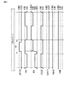
図7は、時系列に繰り返される記憶期間及び表示期間における走査信号GATEA、共通信号VCOM、補助容量信号CS(FRP)、表示信号SIG(xFRP)、画素電位PIXの変化を示すタイミングチャートである。この例においては、表示領域DAの全ての副画素SPXを連続的に白表示とする場合を想定している。なお、ここでは記憶期間が1つのフレーム期間TFで構成され、表示期間が2つのフレーム期間TFで構成されている。但し、記憶期間及び表示期間は、より多くのフレーム期間TFで構成されても良い。
例えば、電圧VSSを0V、電圧VDDを3.2Vとすると、電圧VDDx2は約6.4Vとなる。この場合、図8(a)(b)で発生する各電界は、いずれも3.2Vの電位差に起因したものとなる。
以下、フラッシング現象による表示品位の低下を抑制するための実施形態を開示する。
第1実施形態においては、表示期間から記憶期間への移行の際、表示期間の共通信号VCOM及び補助容量信号CS(FRP)の電位を記憶期間においても維持することにより、フラッシング現象を抑制する。以下、本実施形態の詳細を説明する。
以上説明した他にも、本実施形態からは種々の好適な効果を得ることができる。
第2実施形態においては、記憶期間を短くすることにより、フラッシング現象を人の目で捉えにくくする。以下、本実施形態の詳細を説明する。
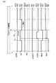
図11は、第2実施形態に係る表示装置1の動作の一例を示すタイミングチャートである。この図においては、図7の場合と同じく、副画素SPXが白表示となる場合を想定して、時系列の表示期間0、記憶期間1、表示期間1、記憶期間2、表示期間2における各信号の電位を示している。
本実施形態では、第1実施形態と同じく、交流駆動回路20の出力を制御することでフラッシング現象を抑制しており、新たな配線や素子を用いていない。したがって、副画素SPXの精細度の低下や、回路パターンの密度増加による製造歩留りの悪化などのデメリットが発生しない。
以上説明した他にも、本実施形態からは種々の好適な効果を得ることができる。
第3実施形態においては、画素電位PIXが所定の条件を満たす場合に表示期間から記憶期間への移行を可能とすることで、フラッシング現象の発生を防止する。以下、本実施形態の詳細を説明する。
図12は、第3実施形態に係る表示装置1の動作の一例を示すタイミングチャートである。この図においては、図7の場合と同じく、副画素SPXが白表示となる場合を想定して、時系列の表示期間0、記憶期間1、表示期間1、記憶期間2、表示期間2における各信号の電位を示している。
以上説明した他にも、本実施形態からは種々の好適な効果を得ることができる。
第1乃至第3実施形態においては、図7乃至図9にて説明した問題点を解消するための方法を開示した。ここで、デジタルモードにおいて生じ得る他の問題点につき、図13のタイミングチャートを用いて説明する。
表示期間から記憶期間へ移行する際に、走査信号GATEAが電圧VSS2に立ち下り、スイッチング素子Q1,Q2がオフされる。これにより、選択信号線12aと画素電極PEとが電気的に遮断されて、画素電極PEがフローティングとなる。走査信号GATEAが立ち下がる際には、画素電極PEと走査線Gとの容量結合により、画素電位PIXも所定の電位ΔVだけ低下し得る。この場合、記憶期間において副画素SPXの輝度変化が生じ、表示品位が低下する。
図14は、第4実施形態に係る表示装置1の動作の一例を示すタイミングチャートである。このタイミングチャートは、第1実施形態に係る動作に本実施形態を適用した例である。交流駆動回路20は、表示期間から記憶期間へ移行するにあたり、走査信号GATEAが立ち下がるタイミングよりも僅かに早いタイミングで、共通信号VCOM及び補助容量信号CSの電位を既定量(図の例ではΔV)だけ低下させる。
なお、図14の例では上記既定量が電位ΔVである場合を示したが、上記既定量はΔVと完全に一致する必要はない。例えば、上記既定量がΔVより小さい値であっても、記憶期間における輝度変化の低減に寄与し得る。
また、交流駆動回路20は、記憶期間の全てに亘って共通信号VCOMを上記既定量だけ低下させ続けても良い。
以上、本発明のいくつかの実施形態を説明したが、これらの実施形態は、例として提示したものであり、発明の範囲を限定することは意図していない。これら新規な実施形態は、その他の様々な形態で実施されることが可能であり、発明の要旨を逸脱しない範囲で、種々の省略、置き換え、変更を行うことができる。これら実施形態やその変形は、発明の範囲や要旨に含まれるとともに、特許請求の範囲に記載された発明とその均等の範囲に含まれる。
また、各実施形態ではアナログモード及びデジタルモードの機能を備える表示装置を開示したが、各実施形態における表示装置の動作はデジタルモードの機能のみを備える表示装置に適用することもできる。
Claims (8)
- 複数の画素が配置された表示領域を有する一対の基板と、
前記一対の基板の間に封入された液晶層と、
前記複数の画素のそれぞれに配置された画素電極と、
前記画素電極と対向し、前記画素電極との間で前記液晶層を駆動する電位差を発生させる共通電極と、
画像データに応じたデジタル信号が供給される信号線と、
前記信号線に前記デジタル信号を供給する第1駆動回路と、
前記共通電極に交流の共通信号を供給する第2駆動回路と、
前記表示領域において、前記複数の画素のそれぞれに配置されたメモリと、
画像の表示信号が供給される第1駆動線と、
画像の非表示信号が供給される第2駆動線と、
記憶期間において、前記信号線に供給された前記デジタル信号を前記メモリに記憶させる記憶制御回路と、
表示期間において、前記第1駆動線に供給される前記表示信号及び前記第2駆動線に供給される前記非表示信号のうち、前記メモリに記憶された前記デジタル信号に対応する一方を選択的に前記画素電極に供給する選択制御回路と、を備え、
前記表示期間において、前記第2駆動回路は、前記表示領域に配置された前記複数の画素の前記画素電極と前記共通電極の電位の極性を1フレーム期間毎に周期的に反転させ、
前記1フレーム期間の開始に同期して前記表示期間から前記記憶期間へ移行する際、前記第2駆動回路は、前記表示期間の前記共通信号の電位を前記記憶期間においても維持する、表示装置。 - 複数の画素が配置された表示領域を有する一対の基板と、
前記一対の基板の間に封入された液晶層と、
前記複数の画素のそれぞれに配置された画素電極と、
前記画素電極と対向し、前記画素電極との間で前記液晶層を駆動する電位差を発生させる共通電極と、
画像データに応じたデジタル信号が供給される信号線と、
前記信号線に前記デジタル信号を供給する第1駆動回路と、
前記共通電極に交流の共通信号を供給する第2駆動回路と、
前記表示領域において、前記複数の画素のそれぞれに配置されたメモリと、
画像の表示信号が供給される第1駆動線と、
画像の非表示信号が供給される第2駆動線と、
記憶期間において、前記信号線に供給された前記デジタル信号を前記メモリに記憶させる記憶制御回路と、
表示期間において、前記第1駆動線に供給される表示信号及び前記第2駆動線に供給される非表示信号のうち、前記メモリに記憶された前記デジタル信号に対応する一方を選択的に前記画素電極に供給する選択制御回路と、
前記表示期間から前記記憶期間への移行の可否を判定する制御装置と、を備え、
前記表示信号は、第1電位と第2電位とを含み、
前記記憶期間において前記メモリに記憶される前記デジタル信号の電位が第3電位であり、
前記制御装置は、
前記第1電位と前記第2電位のうち前記第3電位との電位差が小さい方の電位が、前記記憶期間の開始直前の前記画素電極の電位である場合に、前記記憶期間において前記第3電位を前記メモリに記憶させる動作を行い、
前記第1電位と前記第2電位のうち前記第3電位との電位差が大きい方の電位が、前記記憶期間の開始直前の前記画素電極の電位である場合に、前記記憶期間において前記第3電位を前記メモリに記憶させる動作を行わず、前記表示期間を継続させる、表示装置。 - 前記選択制御回路は、
前記第1駆動線及び前記第2駆動線のうち前記メモリに記憶された前記デジタル信号に対応する一方と接続される選択信号線と、
前記選択信号線と前記画素電極とを電気的に接続又は遮断するスイッチング素子と、
を備え、
前記記憶期間において、前記スイッチング素子は、前記選択信号線と前記画素電極とを電気的に遮断する、
請求項1又は2に記載の表示装置。 - 前記表示期間から前記記憶期間への移行の際、前記スイッチング素子が前記選択信号線と前記画素電極とを電気的に遮断する前に、前記第2駆動回路は、前記共通信号の電位を既定量だけ低下させる、請求項3に記載の表示装置。
- 前記表示期間において、前記画素電極と前記共通電極との間の電位の極性が周期的に反転される、請求項1乃至4のうちいずれか1項に記載の表示装置。
- 前記信号線は、隣り合う前記画素の間を通って延び、
前記一対の基板の少なくとも一方は、光を遮光する遮光層を備え、
前記遮光層は、前記表示領域において、隣り合う前記画素の間にある前記信号線と重畳しない、請求項1乃至5のうちいずれか1項に記載の表示装置。 - 前記一対の基板は、第1基板と、第2基板とを含み、
前記画素電極は、前記第1基板に配置され、
前記第1基板は、前記第2基板に入射して前記液晶層を通り前記第1基板に到達した光を前記第2基板の方向へ反射する反射層を備え、
前記反射層が反射した光により画像を表示する、請求項1乃至6のうちいずれか1項に記載の表示装置。 - デジタルモードとアナログモードとを有し、
前記第1駆動線と前記信号線とは同じ配線であり、
前記デジタルモードにおいては、前記記憶期間及び前記表示期間の動作が実行され、
前記アナログモードにおいては、前記第1駆動線に画像の階調に応じた信号が供給される、請求項1乃至7のうちいずれか1項に記載の表示装置。
Priority Applications (5)
| Application Number | Priority Date | Filing Date | Title |
|---|---|---|---|
| JP2015212091A JP6572095B2 (ja) | 2015-10-28 | 2015-10-28 | 表示装置 |
| US15/277,039 US10438550B2 (en) | 2015-10-28 | 2016-09-27 | Display device |
| CN201610958661.4A CN106898315B (zh) | 2015-10-28 | 2016-10-28 | 显示装置 |
| CN201911131516.9A CN110808014B (zh) | 2015-10-28 | 2016-10-28 | 显示装置 |
| US16/538,455 US10923055B2 (en) | 2015-10-28 | 2019-08-12 | Display device |
Applications Claiming Priority (1)
| Application Number | Priority Date | Filing Date | Title |
|---|---|---|---|
| JP2015212091A JP6572095B2 (ja) | 2015-10-28 | 2015-10-28 | 表示装置 |
Publications (3)
| Publication Number | Publication Date |
|---|---|
| JP2017083654A JP2017083654A (ja) | 2017-05-18 |
| JP2017083654A5 JP2017083654A5 (ja) | 2018-12-06 |
| JP6572095B2 true JP6572095B2 (ja) | 2019-09-04 |
Family
ID=58637858
Family Applications (1)
| Application Number | Title | Priority Date | Filing Date |
|---|---|---|---|
| JP2015212091A Active JP6572095B2 (ja) | 2015-10-28 | 2015-10-28 | 表示装置 |
Country Status (3)
| Country | Link |
|---|---|
| US (2) | US10438550B2 (ja) |
| JP (1) | JP6572095B2 (ja) |
| CN (2) | CN110808014B (ja) |
Families Citing this family (6)
| Publication number | Priority date | Publication date | Assignee | Title |
|---|---|---|---|---|
| JP2017083655A (ja) * | 2015-10-28 | 2017-05-18 | 株式会社ジャパンディスプレイ | 表示装置 |
| CN109389954A (zh) * | 2017-08-14 | 2019-02-26 | 京东方科技集团股份有限公司 | 像素电路、显示面板及其驱动方法和显示装置 |
| CN107945763B (zh) * | 2018-01-05 | 2020-06-26 | 京东方科技集团股份有限公司 | 像素电路、阵列基板、显示面板和显示装置 |
| JP6872571B2 (ja) * | 2018-02-20 | 2021-05-19 | セイコーエプソン株式会社 | 電気光学装置及び電子機器 |
| CN108597468B (zh) * | 2018-04-26 | 2019-12-06 | 京东方科技集团股份有限公司 | 像素电路及其驱动方法、显示面板、显示装置、存储介质 |
| CN108899344B (zh) | 2018-06-29 | 2021-02-09 | 京东方科技集团股份有限公司 | 一种oled显示面板、其驱动方法及显示装置 |
Family Cites Families (17)
| Publication number | Priority date | Publication date | Assignee | Title |
|---|---|---|---|---|
| JPH09243995A (ja) | 1996-03-11 | 1997-09-19 | Matsushita Electric Ind Co Ltd | アクティブマトリックスアレイと液晶表示装置及びその駆動方法 |
| JP3530503B2 (ja) * | 2001-05-08 | 2004-05-24 | 三洋電機株式会社 | 表示装置 |
| JP4369710B2 (ja) * | 2003-09-02 | 2009-11-25 | 株式会社 日立ディスプレイズ | 表示装置 |
| KR100680103B1 (ko) * | 2004-02-02 | 2007-02-28 | 샤프 가부시키가이샤 | 액정 표시 장치 |
| WO2007013646A1 (en) * | 2005-07-29 | 2007-02-01 | Semiconductor Energy Laboratory Co., Ltd. | Display device and driving method thereof |
| TW200739507A (en) * | 2006-03-23 | 2007-10-16 | Toshiba Matsushita Display Tec | Liquid crystal display device |
| JP5046226B2 (ja) | 2007-04-02 | 2012-10-10 | 株式会社ジャパンディスプレイウェスト | 画像表示装置 |
| WO2009067010A2 (en) * | 2007-11-21 | 2009-05-28 | Polymer Vision Limited | An electronic device with a flexible display |
| GB0905818D0 (en) * | 2009-04-06 | 2009-05-20 | Airbus Uk Ltd | Coupling assembly |
| TWI412855B (zh) * | 2009-04-09 | 2013-10-21 | Wintek Corp | 液晶顯示裝置及其驅動方法 |
| TWI528342B (zh) * | 2009-09-16 | 2016-04-01 | 半導體能源研究所股份有限公司 | 顯示裝置及其驅動方法 |
| US8698852B2 (en) * | 2010-05-20 | 2014-04-15 | Semiconductor Energy Laboratory Co., Ltd. | Display device and method for driving the same |
| JP5527129B2 (ja) * | 2010-09-16 | 2014-06-18 | セイコーエプソン株式会社 | 電気泳動表示装置、電気泳動表示装置の駆動方法および電子機器 |
| JP5849489B2 (ja) | 2011-07-21 | 2016-01-27 | セイコーエプソン株式会社 | 電気光学装置、投射型表示装置、電子機器、および電気光学装置の製造方法 |
| JP2014071372A (ja) * | 2012-09-28 | 2014-04-21 | Japan Display Inc | 表示装置および電子機器 |
| CN102915719B (zh) * | 2012-11-09 | 2014-09-17 | 福州华映视讯有限公司 | 避免液晶面板烧付和色偏的装置及其方法 |
| CN103995375A (zh) * | 2014-06-06 | 2014-08-20 | 友达光电股份有限公司 | 共通电压补偿电路、补偿方法及其薄膜晶体管液晶显示器 |
-
2015
- 2015-10-28 JP JP2015212091A patent/JP6572095B2/ja active Active
-
2016
- 2016-09-27 US US15/277,039 patent/US10438550B2/en active Active
- 2016-10-28 CN CN201911131516.9A patent/CN110808014B/zh active Active
- 2016-10-28 CN CN201610958661.4A patent/CN106898315B/zh active Active
-
2019
- 2019-08-12 US US16/538,455 patent/US10923055B2/en active Active
Also Published As
| Publication number | Publication date |
|---|---|
| CN106898315A (zh) | 2017-06-27 |
| US20190362682A1 (en) | 2019-11-28 |
| CN110808014B (zh) | 2022-04-01 |
| JP2017083654A (ja) | 2017-05-18 |
| CN110808014A (zh) | 2020-02-18 |
| US10438550B2 (en) | 2019-10-08 |
| US10923055B2 (en) | 2021-02-16 |
| US20170124967A1 (en) | 2017-05-04 |
| CN106898315B (zh) | 2019-11-08 |
Similar Documents
| Publication | Publication Date | Title |
|---|---|---|
| JP6572095B2 (ja) | 表示装置 | |
| JP2017083655A (ja) | 表示装置 | |
| US11308887B2 (en) | Display device having multiple start signals for emission control scanning drivers | |
| JP6607798B2 (ja) | 表示装置 | |
| KR102242892B1 (ko) | 스캔구동부 및 이를 이용한 유기전계발광표시장치 | |
| US9978327B2 (en) | Gate driving circuit and a display device including the gate driving circuit | |
| EP3327496A1 (en) | Liquid crystal display | |
| EP2498243A1 (en) | Display device | |
| JP2017134338A (ja) | 表示装置 | |
| KR102430433B1 (ko) | 표시장치 | |
| JP2008116694A (ja) | 電気光学装置、駆動回路および電子機器 | |
| EP2498244A1 (en) | Pixel circuit and display device | |
| US20210407424A1 (en) | Display panel and display device | |
| JP5446205B2 (ja) | 電気光学装置および駆動回路 | |
| WO2020026954A1 (ja) | 表示装置及びその駆動方法 | |
| JP4349446B2 (ja) | 電気光学装置、駆動回路および電子機器 | |
| JP2010039136A (ja) | 液晶表示装置 | |
| US10109249B2 (en) | Display device | |
| KR102587318B1 (ko) | 게이트 구동회로 및 이를 포함하는 표시장치 | |
| JP7289693B2 (ja) | 表示装置およびその駆動方法 | |
| JP2022078757A (ja) | 表示装置及び表示装置の駆動方法 | |
| JP2019086698A (ja) | 表示装置 | |
| JP2009223173A (ja) | 電気光学装置、駆動回路および電子機器 | |
| JP2010107808A (ja) | 電気光学装置、駆動回路および電子機器 | |
| JP4858521B2 (ja) | 電気光学装置、駆動回路および電子機器 |
Legal Events
| Date | Code | Title | Description |
|---|---|---|---|
| A521 | Request for written amendment filed |
Free format text: JAPANESE INTERMEDIATE CODE: A523 Effective date: 20181023 |
|
| A621 | Written request for application examination |
Free format text: JAPANESE INTERMEDIATE CODE: A621 Effective date: 20181023 |
|
| A977 | Report on retrieval |
Free format text: JAPANESE INTERMEDIATE CODE: A971007 Effective date: 20190626 |
|
| TRDD | Decision of grant or rejection written | ||
| A01 | Written decision to grant a patent or to grant a registration (utility model) |
Free format text: JAPANESE INTERMEDIATE CODE: A01 Effective date: 20190716 |
|
| A61 | First payment of annual fees (during grant procedure) |
Free format text: JAPANESE INTERMEDIATE CODE: A61 Effective date: 20190809 |
|
| R150 | Certificate of patent or registration of utility model |
Ref document number: 6572095 Country of ref document: JP Free format text: JAPANESE INTERMEDIATE CODE: R150 |
|
| R250 | Receipt of annual fees |
Free format text: JAPANESE INTERMEDIATE CODE: R250 |
|
| R250 | Receipt of annual fees |
Free format text: JAPANESE INTERMEDIATE CODE: R250 |