JP6572095B2 - Display device - Google Patents
Display device Download PDFInfo
- Publication number
- JP6572095B2 JP6572095B2 JP2015212091A JP2015212091A JP6572095B2 JP 6572095 B2 JP6572095 B2 JP 6572095B2 JP 2015212091 A JP2015212091 A JP 2015212091A JP 2015212091 A JP2015212091 A JP 2015212091A JP 6572095 B2 JP6572095 B2 JP 6572095B2
- Authority
- JP
- Japan
- Prior art keywords
- display
- signal
- potential
- period
- pixel electrode
- Prior art date
- Legal status (The legal status is an assumption and is not a legal conclusion. Google has not performed a legal analysis and makes no representation as to the accuracy of the status listed.)
- Active
Links
- 238000003860 storage Methods 0.000 claims description 108
- 239000000758 substrate Substances 0.000 claims description 48
- 239000004973 liquid crystal related substance Substances 0.000 claims description 16
- 230000007704 transition Effects 0.000 claims description 7
- 230000000903 blocking effect Effects 0.000 claims 1
- 230000005684 electric field Effects 0.000 description 18
- 102100036464 Activated RNA polymerase II transcriptional coactivator p15 Human genes 0.000 description 17
- 101000713904 Homo sapiens Activated RNA polymerase II transcriptional coactivator p15 Proteins 0.000 description 17
- 229910004444 SUB1 Inorganic materials 0.000 description 17
- 238000011010 flushing procedure Methods 0.000 description 16
- 229910004438 SUB2 Inorganic materials 0.000 description 13
- 101100311330 Schizosaccharomyces pombe (strain 972 / ATCC 24843) uap56 gene Proteins 0.000 description 13
- 101150018444 sub2 gene Proteins 0.000 description 13
- 230000006870 function Effects 0.000 description 12
- 230000007423 decrease Effects 0.000 description 9
- 230000008859 change Effects 0.000 description 6
- 238000000034 method Methods 0.000 description 6
- 230000002093 peripheral effect Effects 0.000 description 5
- 230000006866 deterioration Effects 0.000 description 4
- 230000000694 effects Effects 0.000 description 4
- 239000003990 capacitor Substances 0.000 description 3
- 230000008878 coupling Effects 0.000 description 3
- 238000010168 coupling process Methods 0.000 description 3
- 238000005859 coupling reaction Methods 0.000 description 3
- 238000010586 diagram Methods 0.000 description 2
- 238000004519 manufacturing process Methods 0.000 description 2
- 239000011159 matrix material Substances 0.000 description 2
- 239000010409 thin film Substances 0.000 description 2
- 239000004020 conductor Substances 0.000 description 1
- 238000005401 electroluminescence Methods 0.000 description 1
- AMGQUBHHOARCQH-UHFFFAOYSA-N indium;oxotin Chemical compound [In].[Sn]=O AMGQUBHHOARCQH-UHFFFAOYSA-N 0.000 description 1
- 230000036452 memory potential Effects 0.000 description 1
- 239000007769 metal material Substances 0.000 description 1
- 230000004048 modification Effects 0.000 description 1
- 238000012986 modification Methods 0.000 description 1
- 230000009467 reduction Effects 0.000 description 1
- 238000004904 shortening Methods 0.000 description 1
Images


Classifications
-
- G—PHYSICS
- G09—EDUCATION; CRYPTOGRAPHY; DISPLAY; ADVERTISING; SEALS
- G09G—ARRANGEMENTS OR CIRCUITS FOR CONTROL OF INDICATING DEVICES USING STATIC MEANS TO PRESENT VARIABLE INFORMATION
- G09G3/00—Control arrangements or circuits, of interest only in connection with visual indicators other than cathode-ray tubes
- G09G3/20—Control arrangements or circuits, of interest only in connection with visual indicators other than cathode-ray tubes for presentation of an assembly of a number of characters, e.g. a page, by composing the assembly by combination of individual elements arranged in a matrix no fixed position being assigned to or needed to be assigned to the individual characters or partial characters
- G09G3/34—Control arrangements or circuits, of interest only in connection with visual indicators other than cathode-ray tubes for presentation of an assembly of a number of characters, e.g. a page, by composing the assembly by combination of individual elements arranged in a matrix no fixed position being assigned to or needed to be assigned to the individual characters or partial characters by control of light from an independent source
- G09G3/36—Control arrangements or circuits, of interest only in connection with visual indicators other than cathode-ray tubes for presentation of an assembly of a number of characters, e.g. a page, by composing the assembly by combination of individual elements arranged in a matrix no fixed position being assigned to or needed to be assigned to the individual characters or partial characters by control of light from an independent source using liquid crystals
- G09G3/3611—Control of matrices with row and column drivers
- G09G3/3614—Control of polarity reversal in general
-
- G—PHYSICS
- G09—EDUCATION; CRYPTOGRAPHY; DISPLAY; ADVERTISING; SEALS
- G09G—ARRANGEMENTS OR CIRCUITS FOR CONTROL OF INDICATING DEVICES USING STATIC MEANS TO PRESENT VARIABLE INFORMATION
- G09G3/00—Control arrangements or circuits, of interest only in connection with visual indicators other than cathode-ray tubes
- G09G3/20—Control arrangements or circuits, of interest only in connection with visual indicators other than cathode-ray tubes for presentation of an assembly of a number of characters, e.g. a page, by composing the assembly by combination of individual elements arranged in a matrix no fixed position being assigned to or needed to be assigned to the individual characters or partial characters
- G09G3/34—Control arrangements or circuits, of interest only in connection with visual indicators other than cathode-ray tubes for presentation of an assembly of a number of characters, e.g. a page, by composing the assembly by combination of individual elements arranged in a matrix no fixed position being assigned to or needed to be assigned to the individual characters or partial characters by control of light from an independent source
- G09G3/36—Control arrangements or circuits, of interest only in connection with visual indicators other than cathode-ray tubes for presentation of an assembly of a number of characters, e.g. a page, by composing the assembly by combination of individual elements arranged in a matrix no fixed position being assigned to or needed to be assigned to the individual characters or partial characters by control of light from an independent source using liquid crystals
- G09G3/3611—Control of matrices with row and column drivers
- G09G3/3674—Details of drivers for scan electrodes
- G09G3/3677—Details of drivers for scan electrodes suitable for active matrices only
-
- G—PHYSICS
- G02—OPTICS
- G02F—OPTICAL DEVICES OR ARRANGEMENTS FOR THE CONTROL OF LIGHT BY MODIFICATION OF THE OPTICAL PROPERTIES OF THE MEDIA OF THE ELEMENTS INVOLVED THEREIN; NON-LINEAR OPTICS; FREQUENCY-CHANGING OF LIGHT; OPTICAL LOGIC ELEMENTS; OPTICAL ANALOGUE/DIGITAL CONVERTERS
- G02F1/00—Devices or arrangements for the control of the intensity, colour, phase, polarisation or direction of light arriving from an independent light source, e.g. switching, gating or modulating; Non-linear optics
- G02F1/01—Devices or arrangements for the control of the intensity, colour, phase, polarisation or direction of light arriving from an independent light source, e.g. switching, gating or modulating; Non-linear optics for the control of the intensity, phase, polarisation or colour
- G02F1/13—Devices or arrangements for the control of the intensity, colour, phase, polarisation or direction of light arriving from an independent light source, e.g. switching, gating or modulating; Non-linear optics for the control of the intensity, phase, polarisation or colour based on liquid crystals, e.g. single liquid crystal display cells
- G02F1/133—Constructional arrangements; Operation of liquid crystal cells; Circuit arrangements
- G02F1/136—Liquid crystal cells structurally associated with a semi-conducting layer or substrate, e.g. cells forming part of an integrated circuit
- G02F1/1362—Active matrix addressed cells
- G02F1/13624—Active matrix addressed cells having more than one switching element per pixel
-
- G—PHYSICS
- G02—OPTICS
- G02F—OPTICAL DEVICES OR ARRANGEMENTS FOR THE CONTROL OF LIGHT BY MODIFICATION OF THE OPTICAL PROPERTIES OF THE MEDIA OF THE ELEMENTS INVOLVED THEREIN; NON-LINEAR OPTICS; FREQUENCY-CHANGING OF LIGHT; OPTICAL LOGIC ELEMENTS; OPTICAL ANALOGUE/DIGITAL CONVERTERS
- G02F1/00—Devices or arrangements for the control of the intensity, colour, phase, polarisation or direction of light arriving from an independent light source, e.g. switching, gating or modulating; Non-linear optics
- G02F1/01—Devices or arrangements for the control of the intensity, colour, phase, polarisation or direction of light arriving from an independent light source, e.g. switching, gating or modulating; Non-linear optics for the control of the intensity, phase, polarisation or colour
- G02F1/13—Devices or arrangements for the control of the intensity, colour, phase, polarisation or direction of light arriving from an independent light source, e.g. switching, gating or modulating; Non-linear optics for the control of the intensity, phase, polarisation or colour based on liquid crystals, e.g. single liquid crystal display cells
- G02F1/133—Constructional arrangements; Operation of liquid crystal cells; Circuit arrangements
- G02F1/13306—Circuit arrangements or driving methods for the control of single liquid crystal cells
-
- G—PHYSICS
- G02—OPTICS
- G02F—OPTICAL DEVICES OR ARRANGEMENTS FOR THE CONTROL OF LIGHT BY MODIFICATION OF THE OPTICAL PROPERTIES OF THE MEDIA OF THE ELEMENTS INVOLVED THEREIN; NON-LINEAR OPTICS; FREQUENCY-CHANGING OF LIGHT; OPTICAL LOGIC ELEMENTS; OPTICAL ANALOGUE/DIGITAL CONVERTERS
- G02F1/00—Devices or arrangements for the control of the intensity, colour, phase, polarisation or direction of light arriving from an independent light source, e.g. switching, gating or modulating; Non-linear optics
- G02F1/01—Devices or arrangements for the control of the intensity, colour, phase, polarisation or direction of light arriving from an independent light source, e.g. switching, gating or modulating; Non-linear optics for the control of the intensity, phase, polarisation or colour
- G02F1/13—Devices or arrangements for the control of the intensity, colour, phase, polarisation or direction of light arriving from an independent light source, e.g. switching, gating or modulating; Non-linear optics for the control of the intensity, phase, polarisation or colour based on liquid crystals, e.g. single liquid crystal display cells
- G02F1/133—Constructional arrangements; Operation of liquid crystal cells; Circuit arrangements
- G02F1/1333—Constructional arrangements; Manufacturing methods
- G02F1/1339—Gaskets; Spacers; Sealing of cells
-
- G—PHYSICS
- G02—OPTICS
- G02F—OPTICAL DEVICES OR ARRANGEMENTS FOR THE CONTROL OF LIGHT BY MODIFICATION OF THE OPTICAL PROPERTIES OF THE MEDIA OF THE ELEMENTS INVOLVED THEREIN; NON-LINEAR OPTICS; FREQUENCY-CHANGING OF LIGHT; OPTICAL LOGIC ELEMENTS; OPTICAL ANALOGUE/DIGITAL CONVERTERS
- G02F1/00—Devices or arrangements for the control of the intensity, colour, phase, polarisation or direction of light arriving from an independent light source, e.g. switching, gating or modulating; Non-linear optics
- G02F1/01—Devices or arrangements for the control of the intensity, colour, phase, polarisation or direction of light arriving from an independent light source, e.g. switching, gating or modulating; Non-linear optics for the control of the intensity, phase, polarisation or colour
- G02F1/13—Devices or arrangements for the control of the intensity, colour, phase, polarisation or direction of light arriving from an independent light source, e.g. switching, gating or modulating; Non-linear optics for the control of the intensity, phase, polarisation or colour based on liquid crystals, e.g. single liquid crystal display cells
- G02F1/133—Constructional arrangements; Operation of liquid crystal cells; Circuit arrangements
- G02F1/1333—Constructional arrangements; Manufacturing methods
- G02F1/1343—Electrodes
- G02F1/134309—Electrodes characterised by their geometrical arrangement
-
- G—PHYSICS
- G02—OPTICS
- G02F—OPTICAL DEVICES OR ARRANGEMENTS FOR THE CONTROL OF LIGHT BY MODIFICATION OF THE OPTICAL PROPERTIES OF THE MEDIA OF THE ELEMENTS INVOLVED THEREIN; NON-LINEAR OPTICS; FREQUENCY-CHANGING OF LIGHT; OPTICAL LOGIC ELEMENTS; OPTICAL ANALOGUE/DIGITAL CONVERTERS
- G02F1/00—Devices or arrangements for the control of the intensity, colour, phase, polarisation or direction of light arriving from an independent light source, e.g. switching, gating or modulating; Non-linear optics
- G02F1/01—Devices or arrangements for the control of the intensity, colour, phase, polarisation or direction of light arriving from an independent light source, e.g. switching, gating or modulating; Non-linear optics for the control of the intensity, phase, polarisation or colour
- G02F1/13—Devices or arrangements for the control of the intensity, colour, phase, polarisation or direction of light arriving from an independent light source, e.g. switching, gating or modulating; Non-linear optics for the control of the intensity, phase, polarisation or colour based on liquid crystals, e.g. single liquid crystal display cells
- G02F1/133—Constructional arrangements; Operation of liquid crystal cells; Circuit arrangements
- G02F1/136—Liquid crystal cells structurally associated with a semi-conducting layer or substrate, e.g. cells forming part of an integrated circuit
- G02F1/1362—Active matrix addressed cells
- G02F1/136286—Wiring, e.g. gate line, drain line
-
- G—PHYSICS
- G09—EDUCATION; CRYPTOGRAPHY; DISPLAY; ADVERTISING; SEALS
- G09G—ARRANGEMENTS OR CIRCUITS FOR CONTROL OF INDICATING DEVICES USING STATIC MEANS TO PRESENT VARIABLE INFORMATION
- G09G3/00—Control arrangements or circuits, of interest only in connection with visual indicators other than cathode-ray tubes
- G09G3/20—Control arrangements or circuits, of interest only in connection with visual indicators other than cathode-ray tubes for presentation of an assembly of a number of characters, e.g. a page, by composing the assembly by combination of individual elements arranged in a matrix no fixed position being assigned to or needed to be assigned to the individual characters or partial characters
- G09G3/34—Control arrangements or circuits, of interest only in connection with visual indicators other than cathode-ray tubes for presentation of an assembly of a number of characters, e.g. a page, by composing the assembly by combination of individual elements arranged in a matrix no fixed position being assigned to or needed to be assigned to the individual characters or partial characters by control of light from an independent source
- G09G3/36—Control arrangements or circuits, of interest only in connection with visual indicators other than cathode-ray tubes for presentation of an assembly of a number of characters, e.g. a page, by composing the assembly by combination of individual elements arranged in a matrix no fixed position being assigned to or needed to be assigned to the individual characters or partial characters by control of light from an independent source using liquid crystals
- G09G3/3611—Control of matrices with row and column drivers
- G09G3/3685—Details of drivers for data electrodes
- G09G3/3688—Details of drivers for data electrodes suitable for active matrices only
-
- G—PHYSICS
- G02—OPTICS
- G02F—OPTICAL DEVICES OR ARRANGEMENTS FOR THE CONTROL OF LIGHT BY MODIFICATION OF THE OPTICAL PROPERTIES OF THE MEDIA OF THE ELEMENTS INVOLVED THEREIN; NON-LINEAR OPTICS; FREQUENCY-CHANGING OF LIGHT; OPTICAL LOGIC ELEMENTS; OPTICAL ANALOGUE/DIGITAL CONVERTERS
- G02F1/00—Devices or arrangements for the control of the intensity, colour, phase, polarisation or direction of light arriving from an independent light source, e.g. switching, gating or modulating; Non-linear optics
- G02F1/01—Devices or arrangements for the control of the intensity, colour, phase, polarisation or direction of light arriving from an independent light source, e.g. switching, gating or modulating; Non-linear optics for the control of the intensity, phase, polarisation or colour
- G02F1/13—Devices or arrangements for the control of the intensity, colour, phase, polarisation or direction of light arriving from an independent light source, e.g. switching, gating or modulating; Non-linear optics for the control of the intensity, phase, polarisation or colour based on liquid crystals, e.g. single liquid crystal display cells
- G02F1/133—Constructional arrangements; Operation of liquid crystal cells; Circuit arrangements
- G02F1/1333—Constructional arrangements; Manufacturing methods
- G02F1/1335—Structural association of cells with optical devices, e.g. polarisers or reflectors
- G02F1/133509—Filters, e.g. light shielding masks
- G02F1/133512—Light shielding layers, e.g. black matrix
-
- G—PHYSICS
- G02—OPTICS
- G02F—OPTICAL DEVICES OR ARRANGEMENTS FOR THE CONTROL OF LIGHT BY MODIFICATION OF THE OPTICAL PROPERTIES OF THE MEDIA OF THE ELEMENTS INVOLVED THEREIN; NON-LINEAR OPTICS; FREQUENCY-CHANGING OF LIGHT; OPTICAL LOGIC ELEMENTS; OPTICAL ANALOGUE/DIGITAL CONVERTERS
- G02F1/00—Devices or arrangements for the control of the intensity, colour, phase, polarisation or direction of light arriving from an independent light source, e.g. switching, gating or modulating; Non-linear optics
- G02F1/01—Devices or arrangements for the control of the intensity, colour, phase, polarisation or direction of light arriving from an independent light source, e.g. switching, gating or modulating; Non-linear optics for the control of the intensity, phase, polarisation or colour
- G02F1/13—Devices or arrangements for the control of the intensity, colour, phase, polarisation or direction of light arriving from an independent light source, e.g. switching, gating or modulating; Non-linear optics for the control of the intensity, phase, polarisation or colour based on liquid crystals, e.g. single liquid crystal display cells
- G02F1/133—Constructional arrangements; Operation of liquid crystal cells; Circuit arrangements
- G02F1/1333—Constructional arrangements; Manufacturing methods
- G02F1/1335—Structural association of cells with optical devices, e.g. polarisers or reflectors
- G02F1/133509—Filters, e.g. light shielding masks
- G02F1/133514—Colour filters
-
- G—PHYSICS
- G02—OPTICS
- G02F—OPTICAL DEVICES OR ARRANGEMENTS FOR THE CONTROL OF LIGHT BY MODIFICATION OF THE OPTICAL PROPERTIES OF THE MEDIA OF THE ELEMENTS INVOLVED THEREIN; NON-LINEAR OPTICS; FREQUENCY-CHANGING OF LIGHT; OPTICAL LOGIC ELEMENTS; OPTICAL ANALOGUE/DIGITAL CONVERTERS
- G02F1/00—Devices or arrangements for the control of the intensity, colour, phase, polarisation or direction of light arriving from an independent light source, e.g. switching, gating or modulating; Non-linear optics
- G02F1/01—Devices or arrangements for the control of the intensity, colour, phase, polarisation or direction of light arriving from an independent light source, e.g. switching, gating or modulating; Non-linear optics for the control of the intensity, phase, polarisation or colour
- G02F1/13—Devices or arrangements for the control of the intensity, colour, phase, polarisation or direction of light arriving from an independent light source, e.g. switching, gating or modulating; Non-linear optics for the control of the intensity, phase, polarisation or colour based on liquid crystals, e.g. single liquid crystal display cells
- G02F1/133—Constructional arrangements; Operation of liquid crystal cells; Circuit arrangements
- G02F1/1333—Constructional arrangements; Manufacturing methods
- G02F1/1335—Structural association of cells with optical devices, e.g. polarisers or reflectors
- G02F1/133553—Reflecting elements
-
- G—PHYSICS
- G02—OPTICS
- G02F—OPTICAL DEVICES OR ARRANGEMENTS FOR THE CONTROL OF LIGHT BY MODIFICATION OF THE OPTICAL PROPERTIES OF THE MEDIA OF THE ELEMENTS INVOLVED THEREIN; NON-LINEAR OPTICS; FREQUENCY-CHANGING OF LIGHT; OPTICAL LOGIC ELEMENTS; OPTICAL ANALOGUE/DIGITAL CONVERTERS
- G02F1/00—Devices or arrangements for the control of the intensity, colour, phase, polarisation or direction of light arriving from an independent light source, e.g. switching, gating or modulating; Non-linear optics
- G02F1/01—Devices or arrangements for the control of the intensity, colour, phase, polarisation or direction of light arriving from an independent light source, e.g. switching, gating or modulating; Non-linear optics for the control of the intensity, phase, polarisation or colour
- G02F1/13—Devices or arrangements for the control of the intensity, colour, phase, polarisation or direction of light arriving from an independent light source, e.g. switching, gating or modulating; Non-linear optics for the control of the intensity, phase, polarisation or colour based on liquid crystals, e.g. single liquid crystal display cells
- G02F1/133—Constructional arrangements; Operation of liquid crystal cells; Circuit arrangements
- G02F1/1333—Constructional arrangements; Manufacturing methods
- G02F1/1343—Electrodes
- G02F1/134309—Electrodes characterised by their geometrical arrangement
- G02F1/134345—Subdivided pixels, e.g. for grey scale or redundancy
-
- G—PHYSICS
- G02—OPTICS
- G02F—OPTICAL DEVICES OR ARRANGEMENTS FOR THE CONTROL OF LIGHT BY MODIFICATION OF THE OPTICAL PROPERTIES OF THE MEDIA OF THE ELEMENTS INVOLVED THEREIN; NON-LINEAR OPTICS; FREQUENCY-CHANGING OF LIGHT; OPTICAL LOGIC ELEMENTS; OPTICAL ANALOGUE/DIGITAL CONVERTERS
- G02F1/00—Devices or arrangements for the control of the intensity, colour, phase, polarisation or direction of light arriving from an independent light source, e.g. switching, gating or modulating; Non-linear optics
- G02F1/01—Devices or arrangements for the control of the intensity, colour, phase, polarisation or direction of light arriving from an independent light source, e.g. switching, gating or modulating; Non-linear optics for the control of the intensity, phase, polarisation or colour
- G02F1/13—Devices or arrangements for the control of the intensity, colour, phase, polarisation or direction of light arriving from an independent light source, e.g. switching, gating or modulating; Non-linear optics for the control of the intensity, phase, polarisation or colour based on liquid crystals, e.g. single liquid crystal display cells
- G02F1/133—Constructional arrangements; Operation of liquid crystal cells; Circuit arrangements
- G02F1/136—Liquid crystal cells structurally associated with a semi-conducting layer or substrate, e.g. cells forming part of an integrated circuit
- G02F1/1362—Active matrix addressed cells
- G02F1/1368—Active matrix addressed cells in which the switching element is a three-electrode device
-
- G—PHYSICS
- G02—OPTICS
- G02F—OPTICAL DEVICES OR ARRANGEMENTS FOR THE CONTROL OF LIGHT BY MODIFICATION OF THE OPTICAL PROPERTIES OF THE MEDIA OF THE ELEMENTS INVOLVED THEREIN; NON-LINEAR OPTICS; FREQUENCY-CHANGING OF LIGHT; OPTICAL LOGIC ELEMENTS; OPTICAL ANALOGUE/DIGITAL CONVERTERS
- G02F2201/00—Constructional arrangements not provided for in groups G02F1/00 - G02F7/00
- G02F2201/12—Constructional arrangements not provided for in groups G02F1/00 - G02F7/00 electrode
- G02F2201/121—Constructional arrangements not provided for in groups G02F1/00 - G02F7/00 electrode common or background
-
- G—PHYSICS
- G02—OPTICS
- G02F—OPTICAL DEVICES OR ARRANGEMENTS FOR THE CONTROL OF LIGHT BY MODIFICATION OF THE OPTICAL PROPERTIES OF THE MEDIA OF THE ELEMENTS INVOLVED THEREIN; NON-LINEAR OPTICS; FREQUENCY-CHANGING OF LIGHT; OPTICAL LOGIC ELEMENTS; OPTICAL ANALOGUE/DIGITAL CONVERTERS
- G02F2201/00—Constructional arrangements not provided for in groups G02F1/00 - G02F7/00
- G02F2201/12—Constructional arrangements not provided for in groups G02F1/00 - G02F7/00 electrode
- G02F2201/123—Constructional arrangements not provided for in groups G02F1/00 - G02F7/00 electrode pixel
-
- G—PHYSICS
- G02—OPTICS
- G02F—OPTICAL DEVICES OR ARRANGEMENTS FOR THE CONTROL OF LIGHT BY MODIFICATION OF THE OPTICAL PROPERTIES OF THE MEDIA OF THE ELEMENTS INVOLVED THEREIN; NON-LINEAR OPTICS; FREQUENCY-CHANGING OF LIGHT; OPTICAL LOGIC ELEMENTS; OPTICAL ANALOGUE/DIGITAL CONVERTERS
- G02F2203/00—Function characteristic
- G02F2203/04—Function characteristic wavelength independent
-
- G—PHYSICS
- G09—EDUCATION; CRYPTOGRAPHY; DISPLAY; ADVERTISING; SEALS
- G09G—ARRANGEMENTS OR CIRCUITS FOR CONTROL OF INDICATING DEVICES USING STATIC MEANS TO PRESENT VARIABLE INFORMATION
- G09G2300/00—Aspects of the constitution of display devices
- G09G2300/04—Structural and physical details of display devices
- G09G2300/0421—Structural details of the set of electrodes
- G09G2300/0426—Layout of electrodes and connections
-
- G—PHYSICS
- G09—EDUCATION; CRYPTOGRAPHY; DISPLAY; ADVERTISING; SEALS
- G09G—ARRANGEMENTS OR CIRCUITS FOR CONTROL OF INDICATING DEVICES USING STATIC MEANS TO PRESENT VARIABLE INFORMATION
- G09G2300/00—Aspects of the constitution of display devices
- G09G2300/04—Structural and physical details of display devices
- G09G2300/0439—Pixel structures
- G09G2300/0452—Details of colour pixel setup, e.g. pixel composed of a red, a blue and two green components
-
- G—PHYSICS
- G09—EDUCATION; CRYPTOGRAPHY; DISPLAY; ADVERTISING; SEALS
- G09G—ARRANGEMENTS OR CIRCUITS FOR CONTROL OF INDICATING DEVICES USING STATIC MEANS TO PRESENT VARIABLE INFORMATION
- G09G2300/00—Aspects of the constitution of display devices
- G09G2300/08—Active matrix structure, i.e. with use of active elements, inclusive of non-linear two terminal elements, in the pixels together with light emitting or modulating elements
- G09G2300/0809—Several active elements per pixel in active matrix panels
- G09G2300/0842—Several active elements per pixel in active matrix panels forming a memory circuit, e.g. a dynamic memory with one capacitor
- G09G2300/0857—Static memory circuit, e.g. flip-flop
-
- G—PHYSICS
- G09—EDUCATION; CRYPTOGRAPHY; DISPLAY; ADVERTISING; SEALS
- G09G—ARRANGEMENTS OR CIRCUITS FOR CONTROL OF INDICATING DEVICES USING STATIC MEANS TO PRESENT VARIABLE INFORMATION
- G09G2310/00—Command of the display device
- G09G2310/08—Details of timing specific for flat panels, other than clock recovery
Landscapes
- Physics & Mathematics (AREA)
- Engineering & Computer Science (AREA)
- General Physics & Mathematics (AREA)
- Chemical & Material Sciences (AREA)
- Crystallography & Structural Chemistry (AREA)
- Nonlinear Science (AREA)
- Computer Hardware Design (AREA)
- Theoretical Computer Science (AREA)
- Mathematical Physics (AREA)
- Optics & Photonics (AREA)
- Microelectronics & Electronic Packaging (AREA)
- Geometry (AREA)
- Liquid Crystal Display Device Control (AREA)
- Control Of Indicators Other Than Cathode Ray Tubes (AREA)
Description
本発明の実施形態は、表示装置に関する。 Embodiments described herein relate generally to a display device.
表示領域において画素ごとにメモリが配置された液晶表示装置などの表示装置が知られている。この種の表示装置においては、表示させる画像に応じたデジタルデータを各メモリに書き込む記憶期間と、各画素の駆動電位を各メモリに記憶されたデジタルデータに対応する電位に設定することにより表示領域に画像を表示させる表示期間とが交互に繰り返される。このように、メモリに記憶されたデジタルデータに基づいて画素を駆動する方式は、例えば、デジタルモード或いはデジタル駆動方式などと呼ばれる。 A display device such as a liquid crystal display device in which a memory is arranged for each pixel in a display area is known. In this type of display device, a display period is set by setting a storage period in which digital data corresponding to an image to be displayed is written in each memory and a driving potential of each pixel to a potential corresponding to the digital data stored in each memory. The display period in which the image is displayed is alternately repeated. As described above, a method for driving a pixel based on digital data stored in a memory is called, for example, a digital mode or a digital drive method.
また、デジタルモードの機能に加え、各画素の駆動電位を多諧調に変化させるアナログモード(或いはアナログ駆動方式)の機能を備えた表示装置も提案されている。(例えば特許文献1参照) In addition to the digital mode function, a display device having an analog mode (or analog driving method) function that changes the driving potential of each pixel in a multi-tone manner has also been proposed. (For example, see Patent Document 1)
記憶期間及び表示期間の動作をそれぞれ実現するために、各画素には種々の回路やスイッチング素子が設けられる。これらスイッチング素子がオンオフされることで、例えば記憶期間においては画素電極などの要素が電気的にフローティングとなる。フローティングとなった要素の電位は、他の要素の電位変動の影響を受けて変化する。これに起因して、画素において不所望な電界が生じ、画像の輝度変化などを招き得る。 In order to realize the operations in the storage period and the display period, each pixel is provided with various circuits and switching elements. By turning on and off these switching elements, for example, elements such as pixel electrodes are electrically floating during the storage period. The potential of the element that has become floating changes under the influence of potential fluctuations of other elements. As a result, an undesired electric field is generated in the pixel, which may cause a change in luminance of the image.
本開示の一態様における目的は、デジタルモードを採用した表示装置において、表示品位を高めることである。 An object of one embodiment of the present disclosure is to improve display quality in a display device employing a digital mode.
一実施形態に係る表示装置は、複数の画素が配置された表示領域を有する一対の基板と、上記一対の基板の間に封入された液晶層と、上記複数の画素のそれぞれに配置された画素電極と、上記画素電極と対向し、上記画素電極との間で上記液晶層を駆動する電位差を発生させる共通電極と、画像データに応じたデジタル信号が供給される信号線と、上記信号線に上記デジタル信号を供給する第1駆動回路と、上記共通電極に交流の共通信号を供給する第2駆動回路と、上記表示領域において上記複数の画素のそれぞれに配置されたメモリと、画像の表示信号が供給される第1駆動線と、画像の非表示信号が供給される第2駆動線と、記憶期間において上記信号線に供給された上記デジタル信号を上記メモリに記憶させる記憶制御回路と、表示期間において上記第1駆動線に供給される上記表示信号及び上記第2駆動線に供給される上記非表示信号のうち上記メモリに記憶された上記デジタル信号に対応する一方を選択的に上記画素電極に供給する選択制御回路と、を備える。この表示装置において、上記第2駆動回路は、上記表示期間において上記表示領域に配置された上記複数の画素の上記画素電極と上記共通電極の電位の極性を1フレーム期間毎に周期的に反転させ、上記1フレーム期間の開始に同期して上記表示期間から上記記憶期間へ移行する際、上記第2駆動回路は、上記表示期間の上記共通信号の電位を上記記憶期間においても維持する。 A display device according to an embodiment includes a pair of substrates having a display region in which a plurality of pixels are disposed, a liquid crystal layer sealed between the pair of substrates, and pixels disposed in each of the plurality of pixels. A common electrode facing the pixel electrode and generating a potential difference for driving the liquid crystal layer between the pixel electrode, a signal line to which a digital signal corresponding to image data is supplied, and the signal line A first driving circuit for supplying the digital signal; a second driving circuit for supplying an AC common signal to the common electrode; a memory disposed in each of the plurality of pixels in the display region; and an image display signal A first drive line to which an image non-display signal is supplied, a storage control circuit for storing the digital signal supplied to the signal line in a storage period in the memory, and a display Among the display signals supplied to the first drive line and the non-display signal supplied to the second drive line, one of the pixel electrodes corresponding to the digital signal stored in the memory is selectively selected. And a selection control circuit for supplying to. In the display device, the second drive circuit periodically inverts the polarities of the potentials of the pixel electrodes and the common electrode of the plurality of pixels arranged in the display region in the display period every frame period. When the transition from the display period to the storage period is performed in synchronization with the start of the one frame period , the second drive circuit maintains the potential of the common signal in the display period even in the storage period.
いくつかの実施形態につき、図面を参照しながら説明する。
なお、開示はあくまで一例に過ぎず、当業者において、発明の主旨を保っての適宜変更について容易に想到し得るものについては、当然に本発明の範囲に含有される。また、図面は、説明をより明確にするため、実際の態様に比べて模式的に表される場合があるが、あくまで一例であって、本発明の解釈を限定するものではない。各図において、連続して配置される同一又は類似の要素については符号を省略することがある。また、本明細書と各図において、既出の図に関して前述したものと同一又は類似した機能を発揮する構成要素には同一の参照符号を付し、重複する詳細な説明を省略することがある。
Several embodiments will be described with reference to the drawings.
It should be noted that the disclosure is merely an example, and those skilled in the art can easily conceive of appropriate changes while maintaining the gist of the invention are naturally included in the scope of the present invention. In addition, the drawings may be schematically represented in comparison with actual modes in order to clarify the description, but are merely examples, and do not limit the interpretation of the present invention. In each drawing, the reference numerals may be omitted for the same or similar elements arranged in succession. In addition, in the present specification and each drawing, components that perform the same or similar functions as those described above with reference to the previous drawings are denoted by the same reference numerals, and redundant detailed description may be omitted.
各実施形態においては、表示装置の一例として、多諧調の表示信号により画素を駆動するアナログモードの機能と上述のデジタルモードの機能とを備えた反射型の液晶表示装置を開示する。ただし、各実施形態は、他種の表示装置に対する、各実施形態にて開示される個々の技術的思想の適用を妨げるものではない。他種の表示装置としては、有機エレクトロルミネッセンス表示装置などの自発光型の表示装置、或いは電気泳動素子等を有する電子ペーパ型の表示装置などが想定される。 In each embodiment, as an example of a display device, a reflective liquid crystal display device having an analog mode function for driving a pixel by a multi-tone display signal and the above-described digital mode function is disclosed. However, each embodiment does not preclude the application of the individual technical ideas disclosed in each embodiment to other types of display devices. As another type of display device, a self-luminous display device such as an organic electroluminescence display device or an electronic paper display device having an electrophoretic element or the like is assumed.
先ず、図1乃至図5を用いて、各実施形態に共通する表示装置の構成及び動作について述べる。
図1は、表示装置1の概略構成の一例を示す平面図である。表示装置1は、第1基板SUB1と、第2基板SUB2と、液晶層LCとを備えている。第1基板SUB1及び第2基板SUB2は、互いに対向した状態で貼り合わされている。液晶層LCは、第1基板SUB1及び第2基板SUB2の間に封入されている。
First, the configuration and operation of a display device common to each embodiment will be described with reference to FIGS.
FIG. 1 is a plan view illustrating an example of a schematic configuration of the
表示装置1は、表示領域DAを有している。表示領域DAは、第1基板SUB1上の画素PXがマトリクス状に配列した領域に相当する。具体的には、表示領域DAには、多数の画素PXが第1方向X及び第2方向Yに沿ってマトリクス状に配列されている。第1方向X及び第2方向Yは、例えば互いに直交する。画素PXは、赤色(R)、緑色(G)、青色(B)の副画素SPXを含む。本開示においては、副画素SPXを単に“画素”と呼ぶこともある。
The
図1の例においては、1つの画素PXに含まれる副画素SPXが第1方向Xに並んでいる。但し、画素PXのレイアウトは図1の例に限定されない。例えば、画素PXは、白色(W)などの他の色の副画素SPXをさらに含んでも良い。また、1つの画素PXに含まれる副画素SPXのうちの少なくとも一部が第2方向Yに並んでも良い。 In the example of FIG. 1, subpixels SPX included in one pixel PX are arranged in the first direction X. However, the layout of the pixel PX is not limited to the example of FIG. For example, the pixel PX may further include a sub-pixel SPX of another color such as white (W). Further, at least a part of the sub-pixels SPX included in one pixel PX may be arranged in the second direction Y.
表示装置1は、複数の走査線Gと、複数の信号線Sと、制御装置2と、走査線駆動回路3と、信号線駆動回路4(第1駆動回路)とをさらに備えている。各走査線G及び各信号線Sは、第1基板SUB1に形成されている。走査線駆動回路3及び信号線駆動回路4は、例えばその少なくとも一部が第1基板SUB1に形成され、制御装置2に接続されている。各走査線Gは、第1方向Xに沿って走査線駆動回路3から表示領域DAに延出し、第2方向Yに並んでいる。各信号線Sは、第2方向Yに沿って信号線駆動回路4から表示領域DAに延出し、第1方向Xに並んでいる。平面視において、各信号線Sは、第1方向Xに隣り合う副画素SPXの間を通っている。
The
制御装置2は、例えば第1基板SUB1に実装された集積回路であり、外部から入力される画像データに基づき画像表示に必要な各種の信号を出力する信号供給源として機能する。なお、制御装置2は、第1基板SUB1や第2基板SUB2に実装されずに、フレキシブル配線基板などを介してこれら基板に接続されても良い。走査線駆動回路3は、各走査線Gに対して走査信号を順次に供給する。信号線駆動回路4は、マルチプレクサ40を備えている。例えば、マルチプレクサ40は、信号の出力先をRGBの各副画素SPXに接続された3本の信号線Sの間で切り替えるスイッチング素子群である。
The
副画素SPXの各々は、メモリ10と、画素電極PEとを備えている。メモリ10は、主にデジタルモードにおいて、信号線Sを介して供給されるデジタル信号を記憶する。画素電極PEは、第2基板SUB2に形成された共通電極CEと対向している。共通電極CEは、第1基板SUB1に形成されても良い。画素電極PE及び共通電極CEは、例えばインジウム・ティン・オキサイド(ITO)などの透明導電材料で形成することができる。共通電極CEは、複数の副画素SPXに亘って形成されており、共通電極線LCMを介して制御装置2が備える交流駆動回路20(第2駆動回路)に接続されている。交流駆動回路20には、補助容量線LCSも接続されている。補助容量線LCSは、表示領域DAに延出し、各副画素SPXの回路に接続されている。
Each of the subpixels SPX includes a
表示装置1は、各副画素SPXに対向するカラーフィルタを備えている。これらのカラーフィルタは、対向する副画素SPXの表示色に対応する色を有しており、例えば第2基板SUB2に形成されている。
図2は、第1基板SUB1及び第2基板SUB2の概略的な平面図である。表示領域DAの周囲には、周辺領域FAが形成されている。周辺領域FAは、第1基板SUB1と第2基板SUB2とが平面視で重畳する領域のうち、表示領域DAを除いた領域に相当する。表示装置1は、周辺領域FAの概ね全域と重畳する遮光層5を備えている。遮光層5は、例えば第2基板SUB2に配置されている。遮光層5を設けることで、周辺領域FAからの光漏れや、周辺領域FAに形成された回路及び配線による光の反射を防ぐことができる。
The
FIG. 2 is a schematic plan view of the first substrate SUB1 and the second substrate SUB2. A peripheral area FA is formed around the display area DA. The peripheral area FA corresponds to an area excluding the display area DA in an area where the first substrate SUB1 and the second substrate SUB2 overlap in plan view. The
表示領域DAには、外光を反射する反射層6が配置されている。反射層6は、例えば金属材料で形成することができる。表示装置1は、反射層6により反射された光を利用して画像を表示する。反射層6は、例えば後述の図8及び図9に示すように、画素電極PEの一面に接して第1基板SUB1に形成される。表示装置1は、第2基板SUB2の第1基板SUB1と対向しない面に配置されたフロントライトをさらに備えても良い。また、表示装置1は、第1基板SUB1の第2基板SUB2と対向しない面に配置されたバックライトをさらに備えても良い。例えばフロントライト及びバックライトとしては、表示領域DAに対向する導光板と、この導光板の端部に沿って配置された複数の発光ダイオードとを備える面光源装置を用いることができる。さらに、表示装置1は、反射層6を備えずにバックライトを備えたものであっても良い。
A
例えば、遮光層5は、表示領域DAには配置されていない。すなわち、遮光層5は、表示領域DAにおいて、隣り合う副画素SPXの間にある信号線Sと重畳しない。これにより、各画素PXの開口率を高め、高輝度の画像表示が可能となる。なお、遮光層5は、表示領域DAの一部と重畳しても良い。この場合においては、例えば、走査線Gと重畳するように遮光層5を形成しても良い。
For example, the
図3は、副画素SPXの等価回路の一例を示す図である。各副画素SPXの各々には、上記画素電極PEと、上記メモリ10と、ゲート回路11と、選択制御回路12と、記憶制御回路13とが配置されている。
ゲート回路11は、走査線Gが制御端に接続されるとともに出力端が画素電極PEに接続されたスイッチング素子Q1,Q2を備えている。スイッチング素子Q1,Q2は、例えばダブルゲート型の薄膜トランジスタである。走査線Gには、スイッチング素子Q1,Q2をオンするための走査信号GATEAが供給される。
FIG. 3 is a diagram illustrating an example of an equivalent circuit of the subpixel SPX. In each of the subpixels SPX, the pixel electrode PE, the
The
選択制御回路12は、入力端が信号線Sに接続されたスイッチング素子Q3と、入力端が補助容量線LCSに接続されたスイッチング素子Q4とを備えている。信号線Sには、信号線駆動回路4から表示信号SIG又は第1駆動信号xFRPが供給される。補助容量線LCSには、交流駆動回路20から補助容量信号CS又は第2駆動信号FRPが供給される。補助容量線LCSと画素電極PEとの電位差により、液晶層LCを駆動するための補助容量Cscが形成される。さらに、選択制御回路12は、スイッチング素子Q3,Q4の出力端とスイッチング素子Q2の入力端とを接続する選択信号線12aを備えている。スイッチング素子Q1,Q2がオンされている間、選択信号線12aと画素電極PEとが電気的に接続される。一方で、スイッチング素子Q1,Q2がオフされている間、選択信号線12aと画素電極PEとが電気的に遮断される。
The
図3においては、交流駆動回路20から延出した配線が補助容量線LCS及び共通電極線LCMに分岐している。すなわち、この例では、補助容量線LCSに供給される補助容量信号CS又は第2駆動信号FRPと、共通電極線LCMに供給される共通信号VCOMとが同電位である。
In FIG. 3, the wiring extending from the
メモリ10は、スイッチング素子Q5〜Q8を備えている。スイッチング素子Q5,Q7の入力端には、電源電圧VRAMを供給する第1電源線LP1が接続されている。スイッチング素子Q6,Q8の入力端には、電圧VSSが供給される第2電源線LP2が接続されている。例えば、スイッチング素子Q5,Q7はPMOSトランジスタであり、スイッチング素子Q6,Q8はNMOSトランジスタである。スイッチング素子Q5,Q6は出力端がスイッチング素子Q4の制御端に接続されたCMOS型の第1インバータを構成し、スイッチング素子Q7,Q8は出力端がスイッチング素子Q3の制御端に接続されたCMOS型の第2インバータを構成する。これら第1,第2インバータは、逆方向に並列接続されており、スイッチング素子Q3,Q4のいずれか一方を選択的にオンする。
The
記憶制御回路13は、メモリ10にデジタル信号を記憶させる回路であって、スイッチング素子Q9を備えている。スイッチング素子Q9の入力端は信号線Sに接続され、出力端はスイッチング素子Q5,Q6の制御端に接続されている。スイッチング素子Q9の制御端には、デジタル走査線LGDが接続されている。デジタル走査線LGDには、走査信号GATEDが供給される。
The
スイッチング素子Q1〜Q9は、例えばいずれも薄膜トランジスタであって、第1基板SUB1に形成されている。補助容量線LCS、走査線G、第1電源線LP1、第2電源線LP2、デジタル走査線LGDも第1基板SUB1に形成されており、第1方向Xに並ぶ複数の副画素SPXに接続されている。第1電源線LP1、第2電源線LP2、デジタル走査線LGDの信号は、例えば制御装置2から供給される。
The switching elements Q1 to Q9 are all thin film transistors, for example, and are formed on the first substrate SUB1. The auxiliary capacitance line LCS, the scanning line G, the first power supply line LP1, the second power supply line LP2, and the digital scanning line LGD are also formed on the first substrate SUB1 and connected to the plurality of subpixels SPX arranged in the first direction X. ing. Signals of the first power supply line LP1, the second power supply line LP2, and the digital scanning line LGD are supplied from the
以上のような構成の表示装置1は、アナログモード及びデジタルモードの双方で各副画素SPXを駆動することができる。アナログモードは、信号線Sに供給される表示信号に基づき各副画素SPXの輝度を多諧調に制御する方式である。デジタルモードは、メモリ10が記憶するデジタルデータに基づき副画素SPXの輝度を単純にオンオフのモノクロで制御する方式である。以下の説明では、表示装置1がノーマリブラックモードの表示装置であって、デジタルモードにおいてメモリ10がHレベル(高電位レベル)に設定されているときに副画素SPXがオン(白表示)され、メモリ10がLレベル(低電位レベル)に設定されているときに副画素SPXがオフ(黒表示)される場合を想定する。
The
以下、アナログモード及びデジタルモードにおける表示装置1の基本的な動作を説明する。
(アナログモード)
アナログモードにおいては、走査線Gに走査パルスが順次供給されるとともに、走査パルスが供給された走査線Gに対応する各副画素SPXの画像データに応じた多諧調の表示信号が各信号線Sに順次供給される。これにより、第1方向Xに並ぶ一群の副画素SPX(以下、一水平ラインと呼ぶ)ごとに、画像データに応じた電位が順次書き込まれていく。
Hereinafter, basic operations of the
(Analog mode)
In the analog mode, the scanning pulse is sequentially supplied to the scanning line G, and a multi-tone display signal corresponding to the image data of each sub-pixel SPX corresponding to the scanning line G to which the scanning pulse is supplied is displayed on each signal line S. Are sequentially supplied. As a result, for each group of subpixels SPX (hereinafter referred to as one horizontal line) arranged in the first direction X, potentials corresponding to image data are sequentially written.
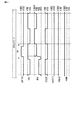
図4は、表示装置1のアナログモードにおける動作の一例を示すタイミングチャートである。このタイミングチャートにおいては、図3に示した1つの副画素SPXに着目して、走査線Gに供給される走査信号GATEA、信号線Sに供給される表示信号SIG、画素電極PEの画素電位PIX、共通電極CEに供給される共通信号VCOM、デジタル走査線LGDに供給される走査信号GATED、第1電源線LP1に供給される電源電圧VRAM、メモリ10に記憶されるメモリ電位RAMの変化を示している。以下の説明においては、一水平ラインに対して画素電位PIXを書き込むための期間を、水平期間THと定義する。
FIG. 4 is a timing chart showing an example of the operation of the
アナログモードにおいては、メモリ10がHレベルに設定されている。Hレベルを設定するための動作は、後述の図5の動作と同様である。メモリ10がHレベルに設定され、電源電圧VRAMが電圧VDDから副画素SPXの駆動電圧である電圧VDD2に立ち上げられたとき、メモリ10からスイッチング素子Q3に電圧VDD2が供給される。これにより、スイッチング素子Q3がオンされる。一方で、スイッチング素子Q4はオフされる。
In the analog mode, the
走査線Gの走査信号GATEAが電圧VSS2から電圧VDD2に立ち上げられると(走査パルスが入力されると)、スイッチング素子Q1,Q2がオンし、画素電極PEが信号線Sに接続される。このとき、図中に矢印で示したように、画素電位PIXが信号線Sに供給された多諧調の表示信号SIGのレベルに設定される。走査信号GATEAが電圧VSS2に立ち下がった後は、画素電極PEがフローティングとなり、補助容量Cscにより画素電極PEと共通電極CEとの間の電位差が維持される。したがって、この副画素SPXは、書き込まれた画素電位PIXに応じた階調の色を、次に画素電位PIXが書き換えられるまで表示する。 When the scanning signal GATEA of the scanning line G rises from the voltage VSS2 to the voltage VDD2 (when a scanning pulse is input), the switching elements Q1 and Q2 are turned on and the pixel electrode PE is connected to the signal line S. At this time, the pixel potential PIX is set to the level of the multi-tone display signal SIG supplied to the signal line S as indicated by an arrow in the drawing. After the scanning signal GATEA falls to the voltage VSS2, the pixel electrode PE is in a floating state, and the potential difference between the pixel electrode PE and the common electrode CE is maintained by the auxiliary capacitor Csc. Therefore, the sub-pixel SPX displays the color of gradation corresponding to the written pixel potential PIX until the pixel potential PIX is rewritten next time.
図4の例では、一水平ラインごとに画素電極PE及び共通電極CEの間の電位の極性を反転させるライン反転制御を用いたケースを示している。したがって、共通信号VCOMの電位は、水平期間THごとに電圧VSS,VDDの間で変化している。 The example of FIG. 4 shows a case in which line inversion control for inverting the polarity of the potential between the pixel electrode PE and the common electrode CE for each horizontal line is shown. Therefore, the potential of the common signal VCOM changes between the voltages VSS and VDD every horizontal period TH.
(デジタルモード)
デジタルモードにおいては、信号線Sに供給されたデジタル信号をメモリ10に記憶させる記憶期間と、第1駆動信号xFRP及び第2駆動信号FRPのうちメモリ10に記憶されたデジタル信号(Hレベル又はLレベル)に対応する一方を選択的に画素電極PEに供給する表示期間とが繰り返される。
(Digital mode)
In the digital mode, a storage period in which the digital signal supplied to the signal line S is stored in the
記憶期間においては、デジタル走査線LGDに走査パルスが順次供給されるとともに、走査パルスが供給されたデジタル走査線LGDに対応する一水平ラインのデジタルの表示信号が各信号線Sに順次供給される。これにより、一水平ラインごとに、画像データに応じたデジタル信号がメモリ10に順次書き込まれていく。
In the storage period, scanning pulses are sequentially supplied to the digital scanning lines LGD, and a digital display signal of one horizontal line corresponding to the digital scanning lines LGD to which the scanning pulses are supplied is sequentially supplied to the signal lines S. . As a result, digital signals corresponding to the image data are sequentially written in the
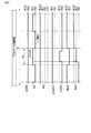
図5は、表示装置1の記憶期間における動作の一例を示すタイミングチャートである。このタイミングチャートにおいては、図4の場合と同じく1つの副画素SPXに着目している。記憶期間においては、走査線Gの走査信号GATEAが電圧VSS2に設定される。したがって、画素電極PEはフローティングとなる。
FIG. 5 is a timing chart showing an example of the operation of the
メモリ10への書き込みを実施する水平期間THにおいて、信号線Sの表示信号SIGは、メモリ10に書き込むべき電位に設定される。ここでは、Hレベルである電圧VDDが白表示に対応し、Lレベルである電圧VSSが黒表示に対応するものとする。第1電源線LP1の電源電圧VRAMは、記憶期間においてメモリ10の電位と同電位にするため、電圧VDD2から電圧VDDに立ち下げられる。その後、デジタル走査線LGDの走査信号GATEDが電圧VSS2から電圧VDD2に立ち上げられると(走査パルスが入力されると)、スイッチング素子Q9がオンし、メモリ10が信号線Sに接続される。このとき、図中に矢印で示したように、信号線Sに供給された表示信号SIGのレベルがメモリ10に書き込まれる。図5においては、Hレベルがメモリ10に書き込まれる場合を例示している。
In the horizontal period TH in which writing to the
その後、走査信号GATEDを電圧VSS2に立ち下げることでスイッチング素子Q9がオフされ、電源電圧VRAMがスイッチング素子Q3,Q4をオンにする電圧であるVDD2に立ち上げられる。この際、メモリ10の電圧もVDDからVDD2に立ち上げられる。これにより、メモリ10は第1電源線LP1とスイッチング素子Q3を接続し、電源電圧VRAMによりスイッチング素子Q3をオンにする。一方で、メモリ10は電源線LP2とスイッチング素子Q4を接続し、電圧VSSによりスイッチング素子Q4をオフにする。スイッチング素子Q3がオンになったことで、画素電極PEに信号線Sの電位が供給される。
Thereafter, by switching the scanning signal GATED to the voltage VSS2, the switching element Q9 is turned off, and the power supply voltage VRAM is raised to VDD2, which is a voltage for turning on the switching elements Q3 and Q4. At this time, the voltage of the
仮に、メモリ10に供給される電位が黒表示に相当するLレベルであれば、メモリ10は第2電源線LP2とスイッチング素子Q3を接続し、電圧VSSによりスイッチング素子Q3をオフにする。一方で、メモリ10は電源線LP1とスイッチング素子Q4を接続し、電源電圧VRAMによりスイッチング素子Q4をオンにする。スイッチング素子Q4がオンになったことで、画素電極PEと補助容量線LCSが接続され共通信号と同電位の信号が供給される。つまり、メモリ10は、記憶した電圧によって、スイッチング素子Q3,Q4のいずれかを排他的にオンにし、信号線S及び補助容量線LCSのいずれか一方を画素電極PEの接続先として選択する。
If the potential supplied to the
図6は、表示装置1の表示期間における動作の一例を示すタイミングチャートである。このタイミングチャートにおいては、図5の場合と同じく1つの副画素SPXに着目している。なお、図5及び図6の例では、画素電極PE及び共通電極CEの間の電位の極性を、表示領域DAに配置された全ての副画素SPXでフレーム期間TFごとに周期的に反転させるフレーム反転制御を用いたケースを示している。1フレームを構成する各水平ラインのメモリ10の書き換えは、例えば1つのフレーム期間TFの間に実行される。すなわち、図5に示した一連の水平期間THは、1つのフレーム期間TFに含まれるものであって、共通信号VCOM及び補助容量信号CSが一定である。一方で、図6に示すように、表示期間は複数のフレーム期間TFで構成されており、フレーム期間TFごとに共通信号VCOM及び補助容量信号CSの電位が電圧VSS,VDDの間で変化している。
FIG. 6 is a timing chart showing an example of the operation of the
表示期間において、フレーム期間TFごとに変化する補助容量信号CSは、交流の第2駆動信号FRPに相当する。また、表示期間においては、信号線Sに第1駆動信号xFRPが供給される。第1駆動信号xFRPは、第2駆動信号FRPと逆相の交流信号であり、フレーム期間TFごとに電圧VDD,VSSの間で変化する。 In the display period, the auxiliary capacitance signal CS that changes every frame period TF corresponds to the AC second drive signal FRP. In the display period, the first drive signal xFRP is supplied to the signal line S. The first drive signal xFRP is an AC signal having a phase opposite to that of the second drive signal FRP, and changes between the voltages VDD and VSS every frame period TF.
表示期間においては、走査線Gの走査信号GATEAが電圧VSS2から電圧VDD2に立ち上げられる。したがって、メモリ10によりスイッチング素子Q3がオンされている場合には信号線Sが画素電極PEに接続され、メモリ10によりスイッチング素子Q4がオンされている場合には補助容量線LCSが画素電極PEに接続される。図6においては、信号線Sが画素電極PEに接続されたことにより、画素電位PIXが第1駆動信号xFRPに設定される場合を例示している。この場合には、画素電極PEと共通電極CEとの間に電圧VDD−電圧VSSの電位差が生じ、副画素SPXが白表示となる。一方で、補助容量線LCSが画素電極PEに接続された場合には、画素電極PEと共通電極CEとの間に電位差が生じず、副画素SPXが黒表示となる。
In the display period, the scanning signal GATEA of the scanning line G is raised from the voltage VSS2 to the voltage VDD2. Therefore, when the switching element Q3 is turned on by the
以上の説明から判るように、信号線Sは、メモリ10に記憶させるデジタルデータが供給される信号線としての機能と、画像の表示信号である第1駆動信号xFRPが供給される第1駆動線としての機能とを兼ねている。また、補助容量線LCSは、補助容量信号CSを供給する信号線としての機能と、画像の非表示信号である第2駆動信号FRPが供給される第2駆動線としての機能とを兼ねている。これにより、表示領域DAにおける配線の数が減るので、副画素SPXを高精細化したり、開口率を高めたりすることが可能となる。
As can be seen from the above description, the signal line S functions as a signal line to which digital data to be stored in the
記憶期間においては、スイッチング素子Q1,Q2がオフされるので、画素電極PEがフローティングとなる。これに伴い生じ得る問題点の一つにつき、図7乃至図9を用いて説明する。
図7は、時系列に繰り返される記憶期間及び表示期間における走査信号GATEA、共通信号VCOM、補助容量信号CS(FRP)、表示信号SIG(xFRP)、画素電位PIXの変化を示すタイミングチャートである。この例においては、表示領域DAの全ての副画素SPXを連続的に白表示とする場合を想定している。なお、ここでは記憶期間が1つのフレーム期間TFで構成され、表示期間が2つのフレーム期間TFで構成されている。但し、記憶期間及び表示期間は、より多くのフレーム期間TFで構成されても良い。
In the storage period, since the switching elements Q1 and Q2 are turned off, the pixel electrode PE is in a floating state. One of the problems that can occur with this will be described with reference to FIGS.
FIG. 7 is a timing chart showing changes in the scanning signal GATEA, the common signal VCOM, the auxiliary capacitance signal CS (FRP), the display signal SIG (xFRP), and the pixel potential PIX in the storage period and the display period repeated in time series. In this example, it is assumed that all the subpixels SPX in the display area DA are continuously displayed in white. Here, the storage period is composed of one frame period TF, and the display period is composed of two frame periods TF. However, the storage period and the display period may be configured with more frame periods TF.
図中左側の記憶期間1においては、メモリ10の電位をHレベルに設定すべく、電圧VDDの表示信号SIG(実線)が供給される。記憶期間1においては走査信号GATEAが電圧VSS2に立ち下げられており、画素電極PEがフローティングである。そのため、画素電位PIX(破線)は、共通信号VCOMの電位上昇に引き寄せられて上昇する。つまり、画素電位PIXは、直前の表示期間0における画素電位PIXと共通信号VCOMとの電位差が維持されるように電圧VDDx2に上昇する。電圧VDDx2は、電圧VDD,VSSの差分の約2倍の電圧である。
In the
記憶期間1に続く表示期間1においては、信号線Sに交流の第1駆動信号xFRPが供給される。表示期間1に続く記憶期間2においては、メモリ10のHレベルの設定を継続すべく、再び電圧VDDの表示信号SIGが供給される。記憶期間2において画素電極PEがフローティングであるため、画素電位PIXは、共通信号VCOMの電位の下降に引き寄せられて下降する。つまり、直前の表示期間1における画素電位PIXと共通信号VCOMとの電位差が維持されるように電圧−VDDに下降する。電圧−VDDは、およそ電圧VDD,VSSの差分に相当する分だけ電圧VSSより低い電圧である。このように、記憶期間2においては、信号線Sと画素電極PEとの間に大きな電位差Vxが生じる。
In the
図8は、(a)記憶期間1の直前の表示期間0、及び、(b)記憶期間1において、副画素SPXに発生する電界の様子を示す断面図である。この図の例では、反射層6が画素電極PEの液晶層LC側の面に形成されている。反射層6は、第2基板SUB2に入射して液晶層LCを通り第1基板SUB1に到達した光を、第2基板SUB2の方向へ反射する。図8(a)においては、画素電極PEが電圧VDDであり、共通電極CEが電圧VSSである。したがって、画素電極PEから共通電極CEに向かう電界が発生する。また、信号線Sが電圧VDDであるために、信号線Sから共通電極CEに向かう電界も発生する。
FIG. 8 is a cross-sectional view showing the state of an electric field generated in the sub-pixel SPX in (a) the display period 0 immediately before the
一方で、図8(b)においては、画素電極PEが電圧VDDx2であり、共通電極CE及び信号線Sが電圧VDDである。したがって、画素電極PEから共通電極CEに向かう電界と、画素電極PEから信号線Sに向かう電界とが発生する。
例えば、電圧VSSを0V、電圧VDDを3.2Vとすると、電圧VDDx2は約6.4Vとなる。この場合、図8(a)(b)で発生する各電界は、いずれも3.2Vの電位差に起因したものとなる。
On the other hand, in FIG. 8B, the pixel electrode PE is at the voltage VDDx2, and the common electrode CE and the signal line S are at the voltage VDD. Accordingly, an electric field from the pixel electrode PE toward the common electrode CE and an electric field from the pixel electrode PE toward the signal line S are generated.
For example, when the voltage VSS is 0V and the voltage VDD is 3.2V, the voltage VDDx2 is about 6.4V. In this case, each electric field generated in FIGS. 8A and 8B is caused by a potential difference of 3.2V.
図9は、(a)記憶期間2の直前の表示期間1、及び、(b)記憶期間2において、副画素SPXに発生する電界の様子を示す断面図である。図9(a)においては、画素電極PE及び信号線Sが電圧VSSであり、共通電極CEが電圧VDDである。したがって、共通電極CEから画素電極PE及び信号線Sに向かう電界が発生する。
FIG. 9 is a cross-sectional view showing the state of the electric field generated in the subpixel SPX in (a) the
一方で、図9(b)においては、画素電極PEが電圧−VDDであり、共通電極CEが電圧VSSであり、信号線Sが電圧VDDである。この場合、共通電極CEから画素電極PEに向かう電界と、信号線Sから画素電極PEに向かう電界とが主に発生する。 On the other hand, in FIG. 9B, the pixel electrode PE is at the voltage −VDD, the common electrode CE is at the voltage VSS, and the signal line S is at the voltage VDD. In this case, an electric field from the common electrode CE to the pixel electrode PE and an electric field from the signal line S to the pixel electrode PE are mainly generated.
例えば、電圧VSSを0V、電圧VDDを3.2Vとすると、電圧−VDDは約−3.2Vとなる。この場合、図9(a)(b)において画素電極PEと共通電極CEとの間に発生する電界は、3.2Vの電位差に起因したものとなる。また、図9(b)において画素電極PEと信号線Sとの間に発生する電界は、6.4Vの電位差Vxに起因した強い電界となる。この強い電界は、図9(b)において破線で囲った領域のように、画素電極PEと共通電極CEとの間の縦電界に影響し、液晶層LCの配向制御能が低下するので、副画素SPXの輝度低下などの不具合が生じ得る。 For example, when the voltage VSS is 0V and the voltage VDD is 3.2V, the voltage −VDD is about −3.2V. In this case, the electric field generated between the pixel electrode PE and the common electrode CE in FIGS. 9A and 9B is caused by a potential difference of 3.2V. In FIG. 9B, the electric field generated between the pixel electrode PE and the signal line S is a strong electric field due to the potential difference Vx of 6.4V. This strong electric field affects the vertical electric field between the pixel electrode PE and the common electrode CE, as in the region surrounded by the broken line in FIG. 9B, and the alignment control ability of the liquid crystal layer LC is reduced. Problems such as a decrease in luminance of the pixel SPX may occur.
図7の下方に、画像が表示された表示領域DA(DISPLAY)を模式的に示している。全ての副画素SPXを連続的に白表示とする場合を想定しているため、基本的には表示領域DAの全てが連続して白表示である。しかしながら、記憶期間2においては、電位差Vxに起因した輝度低下により、表示領域DAの画像が他の期間に比べて暗くなるフラッシング現象が生じる。このようなフラッシング現象は、表示品位の低下を招く一因となる。
A display area DA (DISPLAY) on which an image is displayed is schematically shown in the lower part of FIG. Since it is assumed that all the sub-pixels SPX are continuously displayed in white, basically all the display area DA is continuously displayed in white. However, in the
なお、ここでは白表示の場合について例示したが、黒表示の場合でも同様に、記憶期間において画素電極PEと信号線Sとの間に大きな電位差Vxが形成されて、フラッシング現象が生じ得る。
以下、フラッシング現象による表示品位の低下を抑制するための実施形態を開示する。
Note that although the case of white display is illustrated here, similarly in the case of black display, a large potential difference Vx is formed between the pixel electrode PE and the signal line S in the storage period, and a flushing phenomenon may occur.
Hereinafter, an embodiment for suppressing a decrease in display quality due to a flushing phenomenon will be disclosed.
(第1実施形態)
第1実施形態においては、表示期間から記憶期間への移行の際、表示期間の共通信号VCOM及び補助容量信号CS(FRP)の電位を記憶期間においても維持することにより、フラッシング現象を抑制する。以下、本実施形態の詳細を説明する。
(First embodiment)
In the first embodiment, during the transition from the display period to the storage period, the flushing phenomenon is suppressed by maintaining the potentials of the common signal VCOM and the auxiliary capacitance signal CS (FRP) in the display period even during the storage period. Details of this embodiment will be described below.
図10は、第1実施形態に係る表示装置1の動作の一例を示すタイミングチャートである。この図においては、図7の場合と同じく、副画素SPXが白表示となる場合を想定して、時系列の表示期間0、記憶期間1、表示期間1、記憶期間2、表示期間2における各信号の電位を示している。
FIG. 10 is a timing chart showing an example of the operation of the
記憶期間1の直前、すなわち表示期間0の後半のフレーム期間TFにおいて、共通信号VCOM及び補助容量信号CSの電圧はVSSである。この場合において、交流駆動回路20は、記憶期間1においても共通信号VCOM及び補助容量信号CSの電圧をVSSで維持する。すなわち、交流駆動回路20は、記憶期間1において交流出力を停止する。記憶期間1に続く表示期間1において、交流駆動回路20は、交流出力を再開する。これにより、共通信号VCOM及び補助容量信号CSは、フレーム期間TFごとに電圧VSS,VDDの間で変位する交流信号(FRP)となる。
Immediately before the
記憶期間2の直前、すなわち表示期間1の後半のフレーム期間TFにおいて、共通信号VCOM及び補助容量信号CSの電圧はVDDである。この場合にも、交流駆動回路20は、交流出力を停止して記憶期間2における共通信号VCOM及び補助容量信号CSの電圧をVDDで維持し、記憶期間2に続く表示期間2において交流出力を再開する。
Immediately before the
図10において、表示信号SIG(xFRP)の波形は図7と同じであるが、画素電位PIXの波形は異なる。すなわち、記憶期間1においては、共通信号VCOMが電圧VSSであるために画素電位PIXは電圧VDDとなる。また、記憶期間2においては共通信号VCOMの電圧がVDDであるために画素電位PIXが電圧VSSとなる。
In FIG. 10, the waveform of the display signal SIG (xFRP) is the same as that in FIG. 7, but the waveform of the pixel potential PIX is different. That is, in the
図7の例においては、記憶期間2において画素電極PEと信号線Sとの電位差Vxが電圧VDD,VSSの差分以上に大きくなったが、図10の例においては電位差Vxが電圧VDD,VSSの差分にとどまる。したがって、本実施形態によれば、フラッシング現象が抑制され、表示品位の低下を防止することができる。
In the example of FIG. 7, the potential difference Vx between the pixel electrode PE and the signal line S is larger than the difference between the voltages VDD and VSS in the
なお、ここでは白表示の場合を例にとって説明したが、黒表示の場合でも同様にフラッシング現象を抑制することができる。なお、本実施形態では、記憶期間1及び記憶期間2の両方において共通信号VCOMの交流出力を停止しているが、一部の記憶期間だけ交流出力を停止させても良い。
Although the case of white display has been described here as an example, the flushing phenomenon can be similarly suppressed even in the case of black display. In the present embodiment, the AC output of the common signal VCOM is stopped in both the
本実施形態では、交流駆動回路20の出力を制御することでフラッシング現象を抑制しており、新たな配線や素子を用いていない。したがって、副画素SPXの精細度の低下や、回路パターンの密度増加による製造歩留りの悪化などのデメリットが発生しない。
以上説明した他にも、本実施形態からは種々の好適な効果を得ることができる。
In the present embodiment, the flushing phenomenon is suppressed by controlling the output of the
In addition to the above description, various suitable effects can be obtained from this embodiment.
(第2実施形態)
第2実施形態においては、記憶期間を短くすることにより、フラッシング現象を人の目で捉えにくくする。以下、本実施形態の詳細を説明する。
図11は、第2実施形態に係る表示装置1の動作の一例を示すタイミングチャートである。この図においては、図7の場合と同じく、副画素SPXが白表示となる場合を想定して、時系列の表示期間0、記憶期間1、表示期間1、記憶期間2、表示期間2における各信号の電位を示している。
(Second Embodiment)
In the second embodiment, shortening the storage period makes it difficult to catch the flushing phenomenon with human eyes. Details of this embodiment will be described below.
FIG. 11 is a timing chart showing an example of the operation of the
各表示期間及び各記憶期間における信号の波形は、図7と同様である。但し、図11においては、記憶期間を構成するフレーム期間がTF1であり、表示期間を構成する各フレーム期間がいずれもTF2である。フレーム期間TF1は、フレーム期間TF2よりも短い(TF1<TF2)。 Signal waveforms in each display period and each storage period are the same as those in FIG. However, in FIG. 11, the frame period constituting the storage period is TF1, and each frame period constituting the display period is TF2. The frame period TF1 is shorter than the frame period TF2 (TF1 <TF2).
記憶期間において交流駆動回路20が出力する共通信号VCOM及び補助容量信号CSの周波数は、第1周波数Fq1(hz)である。一方で、表示期間において交流駆動回路20が出力する共通信号VCOM及び補助容量信号CS(FRP)の周波数は、第2周波数Fq2(hz)である。フレーム期間TF1がフレーム期間TF2よりも短いので、第1周波数Fq1は第2周波数Fq2よりも高くなる(Fq1>Fq2)。なお、この周波数は、図10の通り、ある特定の値から極大値又は極小値を経由し、その特定の値に戻る波形の個数を基準としている。
The frequencies of the common signal VCOM and the auxiliary capacitance signal CS output from the
図11の例においては、図7の場合と同様に、記憶期間2において画素電極PEと共通電極CEの電位差Vxが大きくなり、フラッシング現象が生じ得る。しかしながら、第1周波数Fq1が第2周波数Fq2に比べて高いために、記憶期間2において輝度が低下する期間が相対的に短くなり、フラッシング現象が目立たなくなる。
In the example of FIG. 11, as in the case of FIG. 7, the potential difference Vx between the pixel electrode PE and the common electrode CE increases during the
例えば、第1周波数Fq1を第2周波数Fq2の1.5倍以上とすれば、フラッシング現象による表示品位の低下を好適に防止することができる。第1周波数Fq1を第2周波数Fq2の2倍以上とすれば、表示品位の低下を防止する一層高い効果を得ることができる。なお、メモリ10に安定して電位を記憶させるため、第1周波数Fq1は第2周波数Fq2の5倍以下であることが好ましい。
For example, if the first frequency Fq1 is 1.5 times or more the second frequency Fq2, it is possible to suitably prevent display quality from being deteriorated due to the flushing phenomenon. If the first frequency Fq1 is set to be twice or more the second frequency Fq2, it is possible to obtain a higher effect of preventing the display quality from being deteriorated. In order to stably store the potential in the
他の観点から言えば、第1周波数Fq1を90hz以上とすればフラッシング現象が人の目で捉えにくくなり、表示品位の低下を好適に防止することができる。さらに、第1周波数Fq1を120hz以上とすればフラッシング現象が殆ど視認されないので、一層好ましい。なお、第2周波数Fq2は、例えば60Hz程度に定めることができる。なお、メモリ10に安定して電位を記憶させるため、第1周波数Fq1は300hz以下であることが好ましい。
From another point of view, if the first frequency Fq1 is set to 90 hz or more, the flashing phenomenon is difficult to be caught by the human eye, and the deterioration of display quality can be suitably prevented. Furthermore, if the first frequency Fq1 is set to 120 hz or more, the flushing phenomenon is hardly visually recognized. The second frequency Fq2 can be set to about 60 Hz, for example. In order to stably store the potential in the
なお、ここでは白表示の場合を例にとって説明したが、黒表示の場合でも同様にフラッシング現象を抑制することができる。
本実施形態では、第1実施形態と同じく、交流駆動回路20の出力を制御することでフラッシング現象を抑制しており、新たな配線や素子を用いていない。したがって、副画素SPXの精細度の低下や、回路パターンの密度増加による製造歩留りの悪化などのデメリットが発生しない。
以上説明した他にも、本実施形態からは種々の好適な効果を得ることができる。
Although the case of white display has been described here as an example, the flushing phenomenon can be similarly suppressed even in the case of black display.
In the present embodiment, as in the first embodiment, the flushing phenomenon is suppressed by controlling the output of the
In addition to the above description, various suitable effects can be obtained from this embodiment.
(第3実施形態)
第3実施形態においては、画素電位PIXが所定の条件を満たす場合に表示期間から記憶期間への移行を可能とすることで、フラッシング現象の発生を防止する。以下、本実施形態の詳細を説明する。
図12は、第3実施形態に係る表示装置1の動作の一例を示すタイミングチャートである。この図においては、図7の場合と同じく、副画素SPXが白表示となる場合を想定して、時系列の表示期間0、記憶期間1、表示期間1、記憶期間2、表示期間2における各信号の電位を示している。
(Third embodiment)
In the third embodiment, when the pixel potential PIX satisfies a predetermined condition, the transition from the display period to the storage period is enabled to prevent the occurrence of the flushing phenomenon. Details of this embodiment will be described below.
FIG. 12 is a timing chart illustrating an example of the operation of the
本実施形態では、表示期間から記憶期間へ移行する際に、制御装置2がこの移行の可否を判定する。この判定には、電位Va、第1電位V1、第2電位V2、第3電位V3が用いられる。電位Vaは、記憶期間の開始直前の画素電位PIXである。第1電位V1は第1駆動信号xFRPのLレベルの電圧VSSであり、第2電位V2は第1駆動信号xFRPのHレベルの電圧VDDである。第3電位V3は、記憶期間においてメモリ10に記憶される表示信号SIGの電位である。
In this embodiment, when shifting from the display period to the storage period, the
具体的には、制御装置2は、“電位Vaが第1電位V1と第2電位V2のうち第3電位V3との電位差が小さい方の電位である”との実行条件が成立する場合に、記憶期間への移行が可であると判定する。この場合、記憶期間に移行して、第3電位V3をメモリ10に記憶させる動作が行われる。一方で、制御装置2は、上記実行条件が成立しない場合に、記憶期間への移行が不可であると判定する。この場合、本来であれば記憶期間へ移行すべき書込タイミングが到来しても記憶期間に移行せずに、表示期間を所定のフレーム期間TF(例えば1つのフレーム期間TF)だけ延長する。そして、記憶期間への移行が可であるか再び判定し、可であれば記憶期間へ移行する。
Specifically, when the execution condition that the potential Va is a potential having a smaller potential difference between the first potential V1 and the second potential V2 and the third potential V3 is satisfied, It is determined that the transition to the storage period is possible. In this case, the operation moves to the storage period and the third potential V3 is stored in the
図12を参照して具体例を示す。まず、記憶期間1においてメモリ10に記憶させる第3電位V3は、白電位であるVDDである。この場合、第1電位V1(VSS)と第2電位V2(VDD)のうち第3電位V3との電位差が小さい電位は、第3電位V3との電位差が無い第2電位V2となる。記憶期間1を実行すべき書込タイミング1の直前の表示期間0において、電位Vaは第2電位V2である。よって、上記実行条件が成立し、記憶期間への移行が可である。したがって、この書込タイミング1で記憶期間1の動作が実行される。
A specific example is shown with reference to FIG. First, the third potential V3 stored in the
一方で、記憶期間2を実行すべき書込タイミング2の直前の表示期間1において、電位Va(図中では括弧を付している)は第1電位V1である。さらに、記憶期間2においてメモリ10に記憶させる第3電位V3はVDDである。この場合には上記実行条件が成立しないため、記憶期間への移行が不可である。したがって、書込タイミング2では記憶期間2の動作が実行されず、表示期間1が1つのフレーム期間TFだけ延長される。
On the other hand, in the
続いて、延長後に記憶期間2の動作を実行すべき書込タイミング2aの直前の表示期間1(図7の例では延長期間)において、電位Vaは第2電位V2である。この場合には上記実行条件が成立するため、記憶期間への移行が可である。したがって、この書込タイミング2aで記憶期間2の動作が実行される。
Subsequently, the potential Va is the second potential V2 in the display period 1 (extended period in the example of FIG. 7) immediately before the write timing 2a at which the operation of the
なお、図12の例では実行条件が成立しない場合に1つのフレーム期間TFだけ表示期間1が延長される場合を示したが、より多くのフレーム期間TFに亘って表示期間1が延長されても良い。
In the example of FIG. 12, the
また、ここでは表示領域DAに含まれる全ての副画素SPXが白表示となる場合を想定したが、全ての副画素SPXが黒表示となる場合や、白表示の副画素SPXと黒表示の副画素SPXとが混在する場合にも同様の制御を適用できる。白表示の副画素SPXと黒表示の副画素SPXとが混在する場合、1つの書込タイミングにおいて電位Vaと第3電位V3とが異なる副画素SPXが混在することになる。この場合においては、例えば、全ての副画素SPXのうち上記実行条件が成立する副画素SPXの数が所定の閾値以上である場合に表示期間を延長して、記憶期間を後にずらしても良い。また、黒表示の副画素SPXにおけるフラッシング現象は白表示の場合に比べて表示品位に与える影響が小さいことから、白表示の副画素SPXの全てについて実行条件が成立する場合、或いは、白表示の副画素SPXのうち上記実行条件が成立する副画素SPXの数が所定の閾値以上である場合に表示期間を延長して、記憶期間を後にずらしても良い。 Here, it is assumed that all the subpixels SPX included in the display area DA are displayed in white. However, when all the subpixels SPX are displayed in black, the white display subpixel SPX and the black display subpixel are displayed. The same control can be applied even when the pixels SPX coexist. When the white display subpixel SPX and the black display subpixel SPX coexist, subpixels SPX having different potential Va and third potential V3 coexist at one write timing. In this case, for example, the display period may be extended and the storage period may be shifted later when the number of subpixels SPX for which the execution condition is satisfied is equal to or greater than a predetermined threshold among all the subpixels SPX. Further, the flushing phenomenon in the black display subpixel SPX has a smaller influence on the display quality than in the white display. Therefore, when the execution condition is satisfied for all the white display subpixels SPX, or the white display When the number of subpixels SPX that satisfy the above execution condition among the subpixels SPX is equal to or greater than a predetermined threshold, the display period may be extended and the storage period may be shifted later.
本実施形態によれば、記憶期間における表示信号SIGの電位と、この記憶期間の直前の画素電位PIXとが近い値(図12の例では同じ値)となる。したがって、記憶期間においてフローティングとなった画素電極PEの電位が共通電極CEの電位に応じて変動しても、図7に示したような大きな電位差Vxが生じることはない。これにより、フラッシング現象を抑制することができる。
以上説明した他にも、本実施形態からは種々の好適な効果を得ることができる。
According to the present embodiment, the potential of the display signal SIG in the storage period and the pixel potential PIX immediately before the storage period are close to each other (the same value in the example of FIG. 12). Therefore, even if the potential of the pixel electrode PE that has floated during the storage period varies according to the potential of the common electrode CE, the large potential difference Vx as shown in FIG. 7 does not occur. Thereby, the flushing phenomenon can be suppressed.
In addition to the above description, various suitable effects can be obtained from this embodiment.
(第4実施形態)
第1乃至第3実施形態においては、図7乃至図9にて説明した問題点を解消するための方法を開示した。ここで、デジタルモードにおいて生じ得る他の問題点につき、図13のタイミングチャートを用いて説明する。
表示期間から記憶期間へ移行する際に、走査信号GATEAが電圧VSS2に立ち下り、スイッチング素子Q1,Q2がオフされる。これにより、選択信号線12aと画素電極PEとが電気的に遮断されて、画素電極PEがフローティングとなる。走査信号GATEAが立ち下がる際には、画素電極PEと走査線Gとの容量結合により、画素電位PIXも所定の電位ΔVだけ低下し得る。この場合、記憶期間において副画素SPXの輝度変化が生じ、表示品位が低下する。
(Fourth embodiment)
In the first to third embodiments, a method for solving the problems described in FIGS. 7 to 9 has been disclosed. Here, other problems that may occur in the digital mode will be described with reference to the timing chart of FIG.
When shifting from the display period to the storage period, the scanning signal GATEA falls to the voltage VSS2, and the switching elements Q1 and Q2 are turned off. Thereby, the
このような輝度変化を抑制するために、本実施形態では、スイッチング素子Q1,Q2が選択信号線12aと画素電極PEとを遮断する前に、共通信号VCOM及び補助容量信号CSの電位を既定量だけ低下させる。以下、この動作の具体例を示す。
図14は、第4実施形態に係る表示装置1の動作の一例を示すタイミングチャートである。このタイミングチャートは、第1実施形態に係る動作に本実施形態を適用した例である。交流駆動回路20は、表示期間から記憶期間へ移行するにあたり、走査信号GATEAが立ち下がるタイミングよりも僅かに早いタイミングで、共通信号VCOM及び補助容量信号CSの電位を既定量(図の例ではΔV)だけ低下させる。
In order to suppress such a luminance change, in this embodiment, before the switching elements Q1 and Q2 cut off the
FIG. 14 is a timing chart showing an example of the operation of the
走査信号GATEAが立ち下がる際には、走査線Gと画素電極PEとの容量結合により、画素電位PIXが電位ΔVだけ低下する。走査信号GATEAが立ち下がった後に、交流駆動回路20は、共通信号VCOM及び補助容量信号CSの電位を既定量(ΔV)だけ上昇させる。このとき、画素電極PEはフローティングであるので、画素電位PIXは共通信号VCOMの電位上昇に引き寄せられ、ともに既定量(ΔV)だけ上昇する。
When the scanning signal GATEA falls, the pixel potential PIX decreases by the potential ΔV due to capacitive coupling between the scanning line G and the pixel electrode PE. After the scanning signal GATEA falls, the
以上の動作によれば、表示期間における画素電極PEと共通電極CEとの間の電位差が、この表示期間の直後の記憶期間においても維持される。したがって、走査線Gと画素電極PEとの容量結合に起因した輝度変化を防止することができる。
なお、図14の例では上記既定量が電位ΔVである場合を示したが、上記既定量はΔVと完全に一致する必要はない。例えば、上記既定量がΔVより小さい値であっても、記憶期間における輝度変化の低減に寄与し得る。
また、交流駆動回路20は、記憶期間の全てに亘って共通信号VCOMを上記既定量だけ低下させ続けても良い。
According to the above operation, the potential difference between the pixel electrode PE and the common electrode CE in the display period is maintained in the storage period immediately after the display period. Accordingly, it is possible to prevent a change in luminance due to capacitive coupling between the scanning line G and the pixel electrode PE.
Although the example of FIG. 14 shows the case where the predetermined amount is the potential ΔV, the predetermined amount does not need to completely match ΔV. For example, even if the predetermined amount is a value smaller than ΔV, it can contribute to a reduction in luminance change in the storage period.
Further, the
また、図14の例では、第1実施形態に係る動作に本実施形態を適用した場合を例示したが、第2実施形態や第3実施形態に係る動作に本実施形態を適用することもできる。
以上、本発明のいくつかの実施形態を説明したが、これらの実施形態は、例として提示したものであり、発明の範囲を限定することは意図していない。これら新規な実施形態は、その他の様々な形態で実施されることが可能であり、発明の要旨を逸脱しない範囲で、種々の省略、置き換え、変更を行うことができる。これら実施形態やその変形は、発明の範囲や要旨に含まれるとともに、特許請求の範囲に記載された発明とその均等の範囲に含まれる。
In the example of FIG. 14, the case where the present embodiment is applied to the operation according to the first embodiment is illustrated, but the present embodiment can also be applied to the operation according to the second embodiment or the third embodiment. .
As mentioned above, although some embodiment of this invention was described, these embodiment is shown as an example and is not intending limiting the range of invention. These novel embodiments can be implemented in various other forms, and various omissions, replacements, and changes can be made without departing from the scope of the invention. These embodiments and modifications thereof are included in the scope and gist of the invention, and are included in the invention described in the claims and the equivalents thereof.
例えば、各実施形態にて開示した構成は、適宜に組み合わせることができる。
また、各実施形態ではアナログモード及びデジタルモードの機能を備える表示装置を開示したが、各実施形態における表示装置の動作はデジタルモードの機能のみを備える表示装置に適用することもできる。
For example, the configurations disclosed in the embodiments can be combined as appropriate.
Moreover, although each embodiment disclosed the display apparatus provided with the function of analog mode and digital mode, the operation | movement of the display apparatus in each embodiment can also be applied to the display apparatus provided only with the function of digital mode.
1…表示装置、2…制御装置、4…信号線駆動回路、10…メモリ、11…ゲート回路、12…選択制御回路、12a…選択信号線、13…記憶制御回路、20…交流駆動回路、LCS…補助容量線、PE…画素電極、CE…共通電極、LC…液晶層、G…走査線、S…信号線、LP1…第1電源線、LP2…第2電源線、LGD…デジタル走査線、LCM…共通電極線、Q1〜Q9…スイッチング素子、Csc…補助容量。
DESCRIPTION OF
Claims (8)
前記一対の基板の間に封入された液晶層と、
前記複数の画素のそれぞれに配置された画素電極と、
前記画素電極と対向し、前記画素電極との間で前記液晶層を駆動する電位差を発生させる共通電極と、
画像データに応じたデジタル信号が供給される信号線と、
前記信号線に前記デジタル信号を供給する第1駆動回路と、
前記共通電極に交流の共通信号を供給する第2駆動回路と、
前記表示領域において、前記複数の画素のそれぞれに配置されたメモリと、
画像の表示信号が供給される第1駆動線と、
画像の非表示信号が供給される第2駆動線と、
記憶期間において、前記信号線に供給された前記デジタル信号を前記メモリに記憶させる記憶制御回路と、
表示期間において、前記第1駆動線に供給される前記表示信号及び前記第2駆動線に供給される前記非表示信号のうち、前記メモリに記憶された前記デジタル信号に対応する一方を選択的に前記画素電極に供給する選択制御回路と、を備え、
前記表示期間において、前記第2駆動回路は、前記表示領域に配置された前記複数の画素の前記画素電極と前記共通電極の電位の極性を1フレーム期間毎に周期的に反転させ、
前記1フレーム期間の開始に同期して前記表示期間から前記記憶期間へ移行する際、前記第2駆動回路は、前記表示期間の前記共通信号の電位を前記記憶期間においても維持する、表示装置。 A pair of substrates having a display area in which a plurality of pixels are arranged;
A liquid crystal layer sealed between the pair of substrates;
A pixel electrode disposed in each of the plurality of pixels;
A common electrode facing the pixel electrode and generating a potential difference for driving the liquid crystal layer with the pixel electrode;
A signal line to which a digital signal corresponding to image data is supplied;
A first drive circuit for supplying the digital signal to the signal line;
A second drive circuit for supplying an AC common signal to the common electrode;
A memory disposed in each of the plurality of pixels in the display area;
A first drive line to which an image display signal is supplied;
A second drive line to which an image non-display signal is supplied;
A storage control circuit for storing the digital signal supplied to the signal line in the memory in a storage period;
In the display period, one of the display signal supplied to the first drive line and the non-display signal supplied to the second drive line is selectively selected corresponding to the digital signal stored in the memory. A selection control circuit for supplying to the pixel electrode,
In the display period, the second driving circuit periodically inverts the polarities of the potentials of the pixel electrode and the common electrode of the plurality of pixels arranged in the display region every frame period,
The display device , wherein the second drive circuit maintains the potential of the common signal in the display period even in the storage period when shifting from the display period to the storage period in synchronization with the start of the one frame period .
前記一対の基板の間に封入された液晶層と、
前記複数の画素のそれぞれに配置された画素電極と、
前記画素電極と対向し、前記画素電極との間で前記液晶層を駆動する電位差を発生させる共通電極と、
画像データに応じたデジタル信号が供給される信号線と、
前記信号線に前記デジタル信号を供給する第1駆動回路と、
前記共通電極に交流の共通信号を供給する第2駆動回路と、
前記表示領域において、前記複数の画素のそれぞれに配置されたメモリと、
画像の表示信号が供給される第1駆動線と、
画像の非表示信号が供給される第2駆動線と、
記憶期間において、前記信号線に供給された前記デジタル信号を前記メモリに記憶させる記憶制御回路と、
表示期間において、前記第1駆動線に供給される表示信号及び前記第2駆動線に供給される非表示信号のうち、前記メモリに記憶された前記デジタル信号に対応する一方を選択的に前記画素電極に供給する選択制御回路と、
前記表示期間から前記記憶期間への移行の可否を判定する制御装置と、を備え、
前記表示信号は、第1電位と第2電位とを含み、
前記記憶期間において前記メモリに記憶される前記デジタル信号の電位が第3電位であり、
前記制御装置は、
前記第1電位と前記第2電位のうち前記第3電位との電位差が小さい方の電位が、前記記憶期間の開始直前の前記画素電極の電位である場合に、前記記憶期間において前記第3電位を前記メモリに記憶させる動作を行い、
前記第1電位と前記第2電位のうち前記第3電位との電位差が大きい方の電位が、前記記憶期間の開始直前の前記画素電極の電位である場合に、前記記憶期間において前記第3電位を前記メモリに記憶させる動作を行わず、前記表示期間を継続させる、表示装置。 A pair of substrates having a display area in which a plurality of pixels are arranged;
A liquid crystal layer sealed between the pair of substrates;
A pixel electrode disposed in each of the plurality of pixels;
A common electrode facing the pixel electrode and generating a potential difference for driving the liquid crystal layer with the pixel electrode;
A signal line to which a digital signal corresponding to image data is supplied;
A first drive circuit for supplying the digital signal to the signal line;
A second drive circuit for supplying an AC common signal to the common electrode;
A memory disposed in each of the plurality of pixels in the display area;
A first drive line to which an image display signal is supplied;
A second drive line to which an image non-display signal is supplied;
A storage control circuit for storing the digital signal supplied to the signal line in the memory in a storage period;
In the display period, one of the display signal supplied to the first drive line and the non-display signal supplied to the second drive line is selectively selected from the pixels corresponding to the digital signal stored in the memory. A selection control circuit for supplying to the electrodes;
A control device for determining whether or not the display period can be shifted to the storage period ,
The display signal includes a first potential and a second potential,
A potential of the digital signal stored in the memory in the storage period is a third potential;
The controller is
Of the first potential and the second potential, the smaller potential difference between the third potential and the third potential is the potential of the pixel electrode just before the start of the storage period. the performed operation to be stored in said memory,
Of the first potential and the second potential, the potential with the larger potential difference between the third potential and the potential of the pixel electrode immediately before the start of the storage period is the third potential in the storage period. The display device continues the display period without performing the operation of storing the data in the memory .
前記第1駆動線及び前記第2駆動線のうち前記メモリに記憶された前記デジタル信号に対応する一方と接続される選択信号線と、
前記選択信号線と前記画素電極とを電気的に接続又は遮断するスイッチング素子と、
を備え、
前記記憶期間において、前記スイッチング素子は、前記選択信号線と前記画素電極とを電気的に遮断する、
請求項1又は2に記載の表示装置。 The selection control circuit includes:
A selection signal line connected to one of the first drive line and the second drive line corresponding to the digital signal stored in the memory;
A switching element that electrically connects or disconnects the selection signal line and the pixel electrode;
With
In the storage period, the switching element electrically cuts off the selection signal line and the pixel electrode.
The display device according to claim 1.
前記一対の基板の少なくとも一方は、光を遮光する遮光層を備え、
前記遮光層は、前記表示領域において、隣り合う前記画素の間にある前記信号線と重畳しない、請求項1乃至5のうちいずれか1項に記載の表示装置。 The signal line extends between adjacent pixels,
At least one of the pair of substrates includes a light blocking layer that blocks light,
The display device according to claim 1, wherein the light shielding layer does not overlap with the signal line between the adjacent pixels in the display region.
前記画素電極は、前記第1基板に配置され、
前記第1基板は、前記第2基板に入射して前記液晶層を通り前記第1基板に到達した光を前記第2基板の方向へ反射する反射層を備え、
前記反射層が反射した光により画像を表示する、請求項1乃至6のうちいずれか1項に記載の表示装置。 The pair of substrates includes a first substrate and a second substrate,
The pixel electrode is disposed on the first substrate;
The first substrate includes a reflective layer that reflects the light incident on the second substrate and passing through the liquid crystal layer and reaching the first substrate toward the second substrate;
The display device according to claim 1, wherein an image is displayed by light reflected by the reflective layer.
前記第1駆動線と前記信号線とは同じ配線であり、
前記デジタルモードにおいては、前記記憶期間及び前記表示期間の動作が実行され、
前記アナログモードにおいては、前記第1駆動線に画像の階調に応じた信号が供給される、請求項1乃至7のうちいずれか1項に記載の表示装置。 It has a digital mode and an analog mode,
The first drive line and the signal line are the same wiring,
In the digital mode, operations of the storage period and the display period are executed,
The display device according to claim 1, wherein in the analog mode, a signal corresponding to a gradation of an image is supplied to the first drive line.
Priority Applications (5)
| Application Number | Priority Date | Filing Date | Title |
|---|---|---|---|
| JP2015212091A JP6572095B2 (en) | 2015-10-28 | 2015-10-28 | Display device |
| US15/277,039 US10438550B2 (en) | 2015-10-28 | 2016-09-27 | Display device |
| CN201610958661.4A CN106898315B (en) | 2015-10-28 | 2016-10-28 | Display device |
| CN201911131516.9A CN110808014B (en) | 2015-10-28 | 2016-10-28 | Display device |
| US16/538,455 US10923055B2 (en) | 2015-10-28 | 2019-08-12 | Display device |
Applications Claiming Priority (1)
| Application Number | Priority Date | Filing Date | Title |
|---|---|---|---|
| JP2015212091A JP6572095B2 (en) | 2015-10-28 | 2015-10-28 | Display device |
Publications (3)
| Publication Number | Publication Date |
|---|---|
| JP2017083654A JP2017083654A (en) | 2017-05-18 |
| JP2017083654A5 JP2017083654A5 (en) | 2018-12-06 |
| JP6572095B2 true JP6572095B2 (en) | 2019-09-04 |
Family
ID=58637858
Family Applications (1)
| Application Number | Title | Priority Date | Filing Date |
|---|---|---|---|
| JP2015212091A Active JP6572095B2 (en) | 2015-10-28 | 2015-10-28 | Display device |
Country Status (3)
| Country | Link |
|---|---|
| US (2) | US10438550B2 (en) |
| JP (1) | JP6572095B2 (en) |
| CN (2) | CN110808014B (en) |
Families Citing this family (6)
| Publication number | Priority date | Publication date | Assignee | Title |
|---|---|---|---|---|
| JP2017083655A (en) * | 2015-10-28 | 2017-05-18 | 株式会社ジャパンディスプレイ | Display device |
| CN109389954B (en) * | 2017-08-14 | 2024-07-09 | 京东方科技集团股份有限公司 | Pixel circuit, display panel, driving method of display panel and display device |
| CN107945763B (en) * | 2018-01-05 | 2020-06-26 | 京东方科技集团股份有限公司 | Pixel circuit, array substrate, display panel and display device |
| JP6872571B2 (en) * | 2018-02-20 | 2021-05-19 | セイコーエプソン株式会社 | Electro-optics and electronic equipment |
| CN108597468B (en) * | 2018-04-26 | 2019-12-06 | 京东方科技集团股份有限公司 | Pixel circuit, driving method thereof, display panel, display device and storage medium |
| CN108899344B (en) | 2018-06-29 | 2021-02-09 | 京东方科技集团股份有限公司 | OLED display panel, driving method thereof and display device |
Family Cites Families (17)
| Publication number | Priority date | Publication date | Assignee | Title |
|---|---|---|---|---|
| JPH09243995A (en) | 1996-03-11 | 1997-09-19 | Matsushita Electric Ind Co Ltd | Active matrix array, liquid crystal display device and its drive method |
| JP3530503B2 (en) * | 2001-05-08 | 2004-05-24 | 三洋電機株式会社 | Display device |
| JP4369710B2 (en) * | 2003-09-02 | 2009-11-25 | 株式会社 日立ディスプレイズ | Display device |
| KR100680103B1 (en) * | 2004-02-02 | 2007-02-28 | 샤프 가부시키가이샤 | Liquid crystal display device |
| WO2007013646A1 (en) * | 2005-07-29 | 2007-02-01 | Semiconductor Energy Laboratory Co., Ltd. | Display device and driving method thereof |
| TW200739507A (en) * | 2006-03-23 | 2007-10-16 | Toshiba Matsushita Display Tec | Liquid crystal display device |
| JP5046226B2 (en) | 2007-04-02 | 2012-10-10 | 株式会社ジャパンディスプレイウェスト | Image display device |
| US8654519B2 (en) * | 2007-11-21 | 2014-02-18 | Creator Technology B.V. | Electronic device with a flexible display |
| GB0905818D0 (en) * | 2009-04-06 | 2009-05-20 | Airbus Uk Ltd | Coupling assembly |
| TWI412855B (en) * | 2009-04-09 | 2013-10-21 | Wintek Corp | Liquid crystal display and drive method thereof |
| TWI528342B (en) * | 2009-09-16 | 2016-04-01 | 半導體能源研究所股份有限公司 | Display device and driving method thereof |
| US8698852B2 (en) * | 2010-05-20 | 2014-04-15 | Semiconductor Energy Laboratory Co., Ltd. | Display device and method for driving the same |
| JP5527129B2 (en) * | 2010-09-16 | 2014-06-18 | セイコーエプソン株式会社 | Electrophoretic display device, electrophoretic display device driving method, and electronic apparatus |
| JP5849489B2 (en) * | 2011-07-21 | 2016-01-27 | セイコーエプソン株式会社 | Electro-optical device, projection display device, electronic apparatus, and method of manufacturing electro-optical device |
| JP2014071372A (en) * | 2012-09-28 | 2014-04-21 | Japan Display Inc | Display device and electronic equipment |
| CN102915719B (en) * | 2012-11-09 | 2014-09-17 | 福州华映视讯有限公司 | Device and method for preventing burning and color cast of liquid crystal panel |
| CN103995375A (en) * | 2014-06-06 | 2014-08-20 | 友达光电股份有限公司 | General voltage compensation circuit, compensation method and thin film transistor liquid crystal displayer |
-
2015
- 2015-10-28 JP JP2015212091A patent/JP6572095B2/en active Active
-
2016
- 2016-09-27 US US15/277,039 patent/US10438550B2/en active Active
- 2016-10-28 CN CN201911131516.9A patent/CN110808014B/en active Active
- 2016-10-28 CN CN201610958661.4A patent/CN106898315B/en active Active
-
2019
- 2019-08-12 US US16/538,455 patent/US10923055B2/en active Active
Also Published As
| Publication number | Publication date |
|---|---|
| JP2017083654A (en) | 2017-05-18 |
| US20170124967A1 (en) | 2017-05-04 |
| US10438550B2 (en) | 2019-10-08 |
| CN110808014A (en) | 2020-02-18 |
| CN110808014B (en) | 2022-04-01 |
| CN106898315B (en) | 2019-11-08 |
| CN106898315A (en) | 2017-06-27 |
| US20190362682A1 (en) | 2019-11-28 |
| US10923055B2 (en) | 2021-02-16 |
Similar Documents
| Publication | Publication Date | Title |
|---|---|---|
| JP6572095B2 (en) | Display device | |
| JP2017083655A (en) | Display device | |
| US11308887B2 (en) | Display device having multiple start signals for emission control scanning drivers | |
| JP6607798B2 (en) | Display device | |
| KR102242892B1 (en) | Scan Driver and Organic Light Emitting Display Device Using the same | |
| TWI397734B (en) | Liquid crystal display and driving method thereof | |
| US20160210928A1 (en) | Gate driving circuit and a display device including the gate driving circuit | |
| EP2498243A1 (en) | Display device | |
| KR102430433B1 (en) | Display device | |
| JP2017134338A (en) | Display device | |
| US11322094B2 (en) | Display panel and display device | |
| JP2008116694A (en) | Electro-optical device, drive circuit, and electronic apparatus | |
| EP2498244A1 (en) | Pixel circuit and display device | |
| JP5446205B2 (en) | Electro-optical device and drive circuit | |
| WO2020026954A1 (en) | Display device and driving method therefor | |
| US10109249B2 (en) | Display device | |
| JP4349446B2 (en) | Electro-optical device, drive circuit, and electronic device | |
| JP2010039136A (en) | Liquid crystal display | |
| JP2020079932A (en) | Display | |
| KR102587318B1 (en) | Gate driving circuit and display device having the same | |
| JP7289693B2 (en) | Display device and its driving method | |
| JP2022078757A (en) | Display and method for driving display | |
| JP2019086698A (en) | Display device | |
| JP2010107808A (en) | Electro-optic device, drive circuit and electronic equipment | |
| JP4858521B2 (en) | Electro-optical device, drive circuit, and electronic device |
Legal Events
| Date | Code | Title | Description |
|---|---|---|---|
| A521 | Request for written amendment filed |
Free format text: JAPANESE INTERMEDIATE CODE: A523 Effective date: 20181023 |
|
| A621 | Written request for application examination |
Free format text: JAPANESE INTERMEDIATE CODE: A621 Effective date: 20181023 |
|
| A977 | Report on retrieval |
Free format text: JAPANESE INTERMEDIATE CODE: A971007 Effective date: 20190626 |
|
| TRDD | Decision of grant or rejection written | ||
| A01 | Written decision to grant a patent or to grant a registration (utility model) |
Free format text: JAPANESE INTERMEDIATE CODE: A01 Effective date: 20190716 |
|
| A61 | First payment of annual fees (during grant procedure) |
Free format text: JAPANESE INTERMEDIATE CODE: A61 Effective date: 20190809 |
|
| R150 | Certificate of patent or registration of utility model |
Ref document number: 6572095 Country of ref document: JP Free format text: JAPANESE INTERMEDIATE CODE: R150 |
|
| R250 | Receipt of annual fees |
Free format text: JAPANESE INTERMEDIATE CODE: R250 |
|
| R250 | Receipt of annual fees |
Free format text: JAPANESE INTERMEDIATE CODE: R250 |
|
| R250 | Receipt of annual fees |
Free format text: JAPANESE INTERMEDIATE CODE: R250 |