JP6510838B2 - Bonding apparatus and bonding method - Google Patents
Bonding apparatus and bonding method Download PDFInfo
- Publication number
- JP6510838B2 JP6510838B2 JP2015048178A JP2015048178A JP6510838B2 JP 6510838 B2 JP6510838 B2 JP 6510838B2 JP 2015048178 A JP2015048178 A JP 2015048178A JP 2015048178 A JP2015048178 A JP 2015048178A JP 6510838 B2 JP6510838 B2 JP 6510838B2
- Authority
- JP
- Japan
- Prior art keywords
- die
- imaging
- transfer tool
- reference mark
- mounting position
- Prior art date
- Legal status (The legal status is an assumption and is not a legal conclusion. Google has not performed a legal analysis and makes no representation as to the accuracy of the status listed.)
- Active
Links
- 238000000034 method Methods 0.000 title claims description 21
- 238000003384 imaging method Methods 0.000 claims description 153
- 238000001514 detection method Methods 0.000 claims description 38
- 238000012546 transfer Methods 0.000 claims description 28
- 238000012937 correction Methods 0.000 claims description 26
- 230000003287 optical effect Effects 0.000 claims description 14
- 230000000007 visual effect Effects 0.000 claims 1
- 230000036544 posture Effects 0.000 description 20
- 239000000758 substrate Substances 0.000 description 16
- 238000012545 processing Methods 0.000 description 8
- 238000006073 displacement reaction Methods 0.000 description 4
- 238000010586 diagram Methods 0.000 description 3
- 238000010438 heat treatment Methods 0.000 description 3
- 239000004065 semiconductor Substances 0.000 description 2
- 238000011161 development Methods 0.000 description 1
- 230000018109 developmental process Effects 0.000 description 1
- 230000006870 function Effects 0.000 description 1
- 238000003475 lamination Methods 0.000 description 1
- 239000008188 pellet Substances 0.000 description 1
Images


Landscapes
- Engineering & Computer Science (AREA)
- Computer Hardware Design (AREA)
- Microelectronics & Electronic Packaging (AREA)
- Power Engineering (AREA)
- Manufacturing & Machinery (AREA)
- Physics & Mathematics (AREA)
- Condensed Matter Physics & Semiconductors (AREA)
- General Physics & Mathematics (AREA)
- Die Bonding (AREA)
- Wire Bonding (AREA)
- Container, Conveyance, Adherence, Positioning, Of Wafer (AREA)
Description
本発明は、ボンディング装置及びボンディング方法に係わり、ダイをボンディングする実装位置に位置決め精度を向上できるボンディング装置及びボンディング方法に関する。 The present invention relates to a bonding apparatus and a bonding method, and relates to a bonding apparatus and a bonding method capable of improving positioning accuracy at a mounting position for bonding a die.
ダイ(半導体チップ)を配線基板やリードフレームなどの基板に搭載してパッケージを組み立てる工程の一部に、ウェハからダイを吸着し。基板に直接又は一度中間ステージに載置して、ボンディングヘッドで実装するボンディング工程がある。
このようなボンディング装置として引用文献1がある。引用文献1では、ボンディングヘッドの重量化による位置決め精度の低下を防ぐために、重量化をもたらすボンディングヘッドの回転軸をボンディングヘッドに設けず、ボンディングステージ上の基板の回転方向の位置(角度)ずれを、プリサイサステージ(中間ステージ)上のペレット(ダイ)の回転によって補正する技術を開示している。
The die is absorbed from the wafer as part of the process of mounting the die (semiconductor chip) on a substrate such as a wiring substrate or lead frame and assembling the package. There is a bonding process in which the substrate is mounted directly or once on an intermediate stage by a bonding head.
There is cited
一方、昨今のパッケージの小型・薄型化、ダイの薄型化によるchip on chipの積層技術の発達により、ダイのボンディングはより厳しい一桁オーダーのμmの位置決めが必要になってきている。 On the other hand, with recent developments in chip-on-chip lamination technology due to the miniaturization and thinning of packages and thinning of dies, bonding of dies is required to have a more precise positioning of 1 μm on the order of one digit.
従って、単に引用文献1のようにボンディングステージ上の基板の回転ずれの補正だけでは十分な位置決め精度を得られなく、ダイをピックアップする際に、位置と回転角で規定されるダイの姿勢を撮像するピックアップ撮像カメラと、ダイをボンディングする際に、実装位置を撮像する実装撮像カメラ間のボンディングヘッドに対する姿勢ずれが、ダイの実装位置への位置決め精度へ影響することが課題になってきた。
Therefore, simply correcting the rotational displacement of the substrate on the bonding stage as in
本発明は、上記の課題を鑑みてなされたもので、ピックアップ撮像カメラと実装撮像カメラ間の姿勢ずれを補正し、実装位置での位置決め精度の高いボンディング装置及びボンディング方法を提供することにある。 The present invention has been made in view of the above problems, and its object is to provide a bonding apparatus and a bonding method which correct the positional deviation between a pickup imaging camera and a mounting imaging camera and have high positioning accuracy at a mounting position.
本発明は、上記目的を達成するために、第1の撮像視野を有するピックアップ撮像手段と、
ダイの載置位置を撮像できる第2の撮像視野を有する載置位置撮像手段と、
第1の撮像視野内のダイをピックアップして第2の撮像視野内の載置位置にダイを載置し得るダイ移送ツールであって、ダイをピックアップするときは第1の撮像視野内で撮像可能でありダイを載置位置に載置するときは第2の撮像視野内で撮像可能な位置に基準マークを備えたダイ移送ツールと、
第1の撮像視野内で基準マークを検出できる第1の検出手段と、第2の撮像視野内で基準マークを検出できる第2の検出手段と、第1の検出手段と第2の検出手段の結果に基づきダイ移送ツールが保持するダイの載置場所を補正できる補正手段を有するボンディング装置である。
In order to achieve the above object, the present invention provides a pickup imaging means having a first imaging field of view;
Mounting position imaging means having a second imaging field of view capable of imaging the mounting position of the die;
A die transfer tool capable of picking up a die in a first imaging field of view and placing the die at a mounting position in a second imaging field of view, wherein when picking up the die, imaging within the first imaging field of view A die transfer tool having a fiducial mark at a position where imaging is possible within the second imaging view when possible and placing the die in the mounting position;
A first detection unit capable of detecting a reference mark in a first imaging field of view; a second detection unit capable of detecting a reference mark in a second imaging field; a first detection unit and a second detection unit It is a bonding apparatus which has a correction | amendment means which can correct | amend the mounting position of the die | dye which a die transfer tool hold | maintains based on a result.
ここで、ダイ移送ツールは、ダイをボンディングするボンディングヘッドの他、ウェハからピックアップするピックアップヘッド、中間ステージと何か他の場所の間を移動するヘッドを含む。 Here, the die transfer tool includes a bonding head for bonding a die, a pickup head for picking up from a wafer, and a head for moving between an intermediate stage and some other place.
また、ピックアップ撮像手段は、ウェハからダイをピックアップする場合の撮像手段、中間ステージ上に載置されたダイをピックアップする際の撮像手段、他のダイを保持ツールからダイをピックアップする場合の撮像手段など、要するにダイをピックアップする際に撮像できる撮像手段を含む。また、載置位置撮像手段は、ダイを中間ステージに載置する場合の撮像手段、ダイを基板に載置する場合の撮像手段など、ダイを移送する対象部分に載置する際に撮像する撮像手段を含む。
また、ダイを載置するとは、ダイを対象場所に置く場合の他、仮圧着若しくは本圧着等のボンディング行為のいずれも含む。
The pickup imaging means may be an imaging means for picking up the die from the wafer, an imaging means for picking up the die mounted on the intermediate stage, and an imaging means for picking up the other die from the holding tool In other words, it includes an imaging means capable of imaging when picking up a die. In addition, the mounting position imaging unit captures an image when mounting the die on a target portion to be transferred, such as an imaging unit when the die is mounted on the intermediate stage, and an imaging unit when the die is mounted on the substrate. Including means.
In addition to placing the die, in addition to placing the die at a target location, any of bonding acts such as temporary pressure bonding or full pressure bonding is included.
また、補正手段は、ダイ移送ツールのみよる補正に限らず、ダイ移送ツールが保持するダイの載置場所を補正できるような補正手段であれば何でもよく、下記に述べるように、補正方法としてはダイ移送ツールの位置・角度を補正することにより、ダイの載置場所を補正してもよいし、中間ステージの位置・角度を補正することにより、ダイの載置場所を補正してもよいし、その他、要するにダイの載置場所を補正できるような補正手段であれば、何でもよい。 Further, the correction means is not limited to the correction using only the die transfer tool, and any correction means capable of correcting the mounting position of the die held by the die transfer tool may be used. As described below, the correction method is The mounting position of the die may be corrected by correcting the position / angle of the die transfer tool, or the mounting position of the die may be corrected by correcting the position / angle of the intermediate stage. Any other correction means capable of correcting the mounting place of the die may be used.
また、本発明は、第1の検出手段若しくは第2の検出手段は、移送ツールがダイのピックアップ位置からダイの載置位置へ移動する移動方向若しくは移動方向に直交する方向に平面移動させた際に得られる基準マークの軌跡を検出できてもよい。
さらに、本発明は、基準マークは、移送ツールに設けられた2つのプリズムを有する光学系を介してピックアップ撮像手段若しくは載置位置撮像手段で撮像できる基準マークであってもよい。
Further, according to the present invention, when the first detection means or the second detection means moves the transfer tool from the pick-up position of the die to the mounting position of the die in the moving direction perpendicular to the moving direction or the moving direction. It is possible to detect the locus of the reference mark obtained in
Furthermore, in the present invention, the reference mark may be a reference mark that can be imaged by the pickup imaging means or the mounting position imaging means via an optical system having two prisms provided in the transfer tool.
また、本発明は、補正手段は、載置位置に関わる載置面に平行な面内で回転可能な中間ステージを回転させて補正できてもよい。
さらに、本発明は、ダイを反転できると共に、載置位置を有する載置面に平行な面内で回転可能なピックアップ手段を有し、補正手段は、ピックアップ手段を回転させてもよい。
Further, in the present invention, the correction means may be able to correct by rotating the intermediate stage which can rotate in a plane parallel to the mounting surface related to the mounting position.
Furthermore, the present invention may have a pick-up means capable of reversing the die and rotatable in a plane parallel to the placement surface having the placement position, and the correction means may rotate the pick-up means.
また、本発明は、ピックアップ撮像手段により撮像されたダイ移送ツールに備えられた基準マークを検出する第1の検出ステップと、
載置位置撮像手段により撮像された基準マークを検出する第2の検出ステップと、
第1の検出ステップと第2の検出ステップの検出結果に基づきダイ移送ツールが保持するダイの載置場所を補正するステップを有するボンディング方法である。
Further, according to the present invention, there is provided a first detection step of detecting a reference mark provided on a die transfer tool imaged by a pickup imaging means;
A second detection step of detecting a reference mark imaged by the mounting position imaging means;
It is a bonding method including the step of correcting the placement place of the die held by the die transfer tool based on the detection results of the first detection step and the second detection step.
さらに、本発明は、第1の検出ステップ若しくは第2の検出ステップは、ダイ移送ツールがダイのピックアップ位置からダイの載置位置へ移動する移動方向若しくは移動方向に直交する方向に平面移動させた際に得られる基準マークの軌跡に基づき検出するステップであってもよい。
また、本発明は、第1若しくは第2の検出ステップは、移送ツールに設けられた2つのプリズムを有する光学系を介して基準マークが撮像されるステップであってもよい。
Furthermore, according to the present invention, the first detection step or the second detection step is planarly moved in the movement direction in which the die transfer tool moves from the pickup position of the die to the mounting position of the die or in the direction orthogonal to the movement direction. It may be a step of detecting based on the locus of the reference mark obtained at the time.
Also, in the present invention, the first or second detection step may be a step in which the reference mark is imaged through an optical system having two prisms provided on the transfer tool.
さらに、本発明は、補正ステップは、第1の検出ステップ及び第の検出ステップで得られた結果に基づいて載置面に平行な面内で回転可能な中間ステージを回転させて補正するステップであってもよい。
また、本発明は、補正ステップは、ダイを反転し、載置位置を有する載置面に平行な面内で回転可能なピックアップ手段を回転させて補正するステップであってもよい。
Furthermore, according to the present invention, the correction step is a step of rotating and correcting the rotatable intermediate stage in a plane parallel to the mounting surface based on the results obtained in the first detection step and the second detection step. It may be.
Further, in the present invention, the correction step may be a step of inverting the die and rotating and correcting the rotatable pickup means in a plane parallel to the mounting surface having the mounting position.
本発明によれば、ピックアップ撮像カメラと実装撮像カメラ間の姿勢ずれを補正し、実装位置での位置決め精度の高いボンディング装置及びボンディング方法を提供できる。 According to the present invention, it is possible to correct a positional deviation between the pickup imaging camera and the mounting imaging camera, and to provide a bonding apparatus and a bonding method with high positioning accuracy at the mounting position.
以下に本発明の一実施形態を図面等を用いて説明する。なお、以下の説明は、本発明の一実施形態を説明するためのものであり、本願発明の範囲を制限するものではない。従って、当業者であればこれらの各要素若しくは全要素をこれと均等なものに置換した実施形態を採用することが可能であり、これらの実施形態も本願発明の範囲に含まれる。
なお、本書では、各図の説明において、共通な機能を有する構成要素には同一の参照番号を付し、説明の重複をできるだけ避ける。
An embodiment of the present invention will be described below with reference to the drawings and the like. The following description is for describing one embodiment of the present invention, and does not limit the scope of the present invention. Therefore, one skilled in the art can adopt an embodiment in which each or all of these elements are replaced with equivalent ones, and these embodiments are also included in the scope of the present invention.
In the description of the drawings, components having common functions are denoted by the same reference numerals in the description of the respective drawings to avoid duplication of description as much as possible.
図1は、本発明に好適なボンディング装置であるダイボンダの第1の実施例の主要部の概略側面図である。本ダイボンダ100は、ピックアップヘッド13でピックアップしたダイDを一度中間ステージ(保持位置)22に載置し、載置したダイDをボンディングヘッド23で再度ピックアップし、実装位置にボンディングし、基板Pに実装する装置である。
FIG. 1 is a schematic side view of the main part of a first embodiment of a die bonder which is a bonding apparatus suitable for the present invention. The
ダイボンダ100は、ウェハ上のダイDの姿勢を認識する供給ステージ撮像カメラ11と、中間ステージ22に載置されたダイDの姿勢を認識する中間ステージ撮像カメラ21と、アタッチステージ32上の実装位置を認識する実装撮像カメラ31とを有する。
The
本発明で撮像カメラ間の姿勢ずれ補正しなければならないのは、ボンディングヘッド23によるピックアップに関与する中間ステージ撮像カメラ21と、ボンディングヘッド23による実装位置へのボンディングに関与する実装撮像カメラである。本実施例では、中間ステージ撮像カメラ21が本発明におけるピックアップ撮像カメラとなる。
In the present invention, it is the intermediate-
また、ダイボンダ100は、中間ステージ22に設けられた旋回駆動装置25と、中間ステージ22とアタッチステージ32の間に設けられたアンダビジョンカメラ41と、アタッチステージ32に設けられた加熱装置34と、制御装置50と、を有する。
Further, the
旋回駆動装置25は、実装位置を有する実装面に平行な面で中間ステージ22を旋回させ、中間ステージ撮像カメラ21と実装撮像カメラ間の回転角ずれ等を補正する。
The
アンダビジョンカメラ41はボンディングヘッド23が移動中に吸着しているダイDの状態を真下から観察し、加熱装置34はダイDを実装するためにステージ32を加熱する。
The
制御装置50、図示しないCPU(Central processor unit)、制御プログラム格納するROM(Read only memory)やデータ格納するRAM(Random access memory)、コントロールバスをなど有し、ダイボンダ100を構成する各要素を制御し、以下に述べる実装制御を行う。
The
本発明は、ボンディングヘッド23に基準マークを設け、ピックアップ撮像カメラ21と実装撮像カメラ31との姿勢ずれを補正する。
According to the present invention, the
さらに、本実施例では、中間ステージ22を旋回させ、両撮像カメラの回転角ずれを補正する。以下、本実施例では、両撮像カメラとは、ピックアップ撮像カメラである中間ステージ撮像カメラ21と実装撮像カメラ31とをいう。
Furthermore, in the present embodiment, the
図2(a)は、本実施例でおけるボンディングヘッド23の構造を模式的に示す図である。ボンディングヘッド23は、ダイDを吸着保持するコレット23Cと、コレット23Cを昇降させ、実装面の平行な2次元面上を移動させる本体23Hと、基準マークMを有する撮像カメラ姿勢ずれ検出部23Kとを有する。ボンディングヘッド23は、コレットを実装面に平行面で旋回させる旋回軸を有していない。
FIG. 2A schematically shows the structure of the
撮像カメラ姿勢ずれ検出部23Kは、本体23Hから延在し、基準マークMが設けられたマーク部23mと、基準マークMの像をコレット23Cの中心位置23cpを通り、実装面に直交する中心軸23j上に導く光学系23oを有する。なお、図2(a)に示す中心位置23cpは、紙面に平行な辺上に便宜上示している。
The imaging camera posture
本実施例では、光学系23oは、本体23Hの上部に設けられた2つのプリズム23p1、23p2と、それらを本体23Hに支持する光学系支持部23sを有し、プリズム23p2は、その光軸が中心軸23jと一致するように設けられている。光学系としては、例えば他に、一端を基準マークMに面し、他端を前記プリズム23p2の位置で撮像カメラの撮像面に面するように設けられたファイバースコープを用いてもよい。
In this embodiment, the optical system 23o has two prisms 23p1 and 23p2 provided on the upper portion of the
基準マークMは、両撮像カメラのそれぞれの撮像視野に入り、コレット23Cの中心位置23cpからオフセットした位置に設けられている。また、両撮像カメラの撮像面から基準マークMまでの距離Lは、図2(b)に示す撮像カメラの焦点距離WDとなる位置になる距離、即ちL1+L2+L3となる。 The reference mark M is provided at a position offset from the center position 23cp of the collet 23C in each imaging field of view of both imaging cameras. Further, the distance L from the imaging surface of both imaging cameras to the reference mark M is a distance at which the focal distance WD of the imaging camera shown in FIG. 2B is obtained, that is, L1 + L2 + L3.
図3(a)は、図2(a)に示した基準マークMを上から見た図を示す。その他の基準マークのMの形状として図3(b)に示すように三角の切欠き形状をであってもよいし、マーク23mは棒状であってもよい。要は、基準マークMは、マーク部23mとコントラストが採れ、実装位置での位置決め精度を上げるために撮像カメラの分解能で弁別できるほどの形状を有していればよい。
FIG. 3A shows a top view of the reference mark M shown in FIG. The other reference mark M may have a triangular notch shape as shown in FIG. 3B, or the
また、基準マークとして図3(c)に示すような線状形状であってもよい。線状であれば姿勢ずれを検出するためにマーク基準Mを移動させる必要がない利点がある。ダイDの寸法が小さいとき、分解能をさらに上げるために撮像カメラの視野が小さくなり、線状の長さを長くできない場合がある。 Further, the reference mark may have a linear shape as shown in FIG. 3 (c). If it is linear, there is an advantage that it is not necessary to move the mark reference M in order to detect posture deviation. When the size of the die D is small, the field of view of the imaging camera may be reduced to further increase the resolution, and the linear length may not be increased.
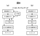
両撮像カメラの姿勢ずれの検出方法を説明する前に、本発明と特許文献1に記載された従来技術を図8を用いて説明する。図8(a)は、本発明の処理フローを模式的に示した図で、図8(b)は、従来技術の処理フローを模式的に示した図である。
Before describing the method of detecting the positional deviation between the two imaging cameras, the present invention and the prior art described in
従来技術は、単に基板とダイの姿勢をそれぞれの撮像カメラで撮像し、基板とダイの位置(X,Y)と回転角θで規定される姿勢ずれを補正している。一方、本発明は、基板とダイの姿勢ずれの補正に加えて、さらに、課題で説明したようにダイの姿勢を撮像するピックアップ撮像カメラと、実装位置(基板等)を撮像する実装撮像カメラ間のボンディングヘッドに対する姿勢ずれ、特に回転角ずれΔθを補正している点である
次に、基準マークMによる撮像カメラの姿勢ずれの検出方法を、実装撮像カメラ31の例を図2、図4及び図5を用いて説明する。図4は、撮像カメラの姿勢ずれの検出処理フローを示す図である。図5(a)は、処理によって得られた実装撮像カメラ31の姿勢ずれの検出結果を示す図である。なお、説明おいて、図1に示すように、ボンディングヘッド23が中間ステージ22とアタッチステージ32との間を移動する方向をY方向とし、実装面32mと平行面においてY方向と直交する方向をX方向とする。
In the prior art, the postures of the substrate and the die are simply imaged by respective imaging cameras, and the posture deviation defined by the positions (X, Y) of the substrate and the die and the rotation angle θ is corrected. On the other hand, according to the present invention, in addition to the correction of the positional deviation between the substrate and the die, the pickup imaging camera for imaging the attitude of the die as described in the problem and the mounted imaging camera for imaging the mounting position (substrate etc.) Position correction with respect to the bonding head, particularly the rotational angle deviation .DELTA..theta .. Next, a method of detecting the attitude deviation of the imaging camera by the reference mark M will be described with reference to FIGS. This will be described with reference to FIG. FIG. 4 is a diagram showing a processing flow of detecting an attitude deviation of the imaging camera. FIG. 5A is a view showing the detection result of the posture deviation of the mounting
まず、ボンディングヘッド23をY方向に移動して実装撮像カメラ31の撮像視野の中心位置付近に移動し、基準マークMの撮像M1を得る(S1)。その後、ボンディングヘッド23をX方向に平行して所定距離移動させ、その時の基準マークMの撮像M2を得る(S2)。図5(a)に示すように、基準マークMをX方向に平行して移動させたにも拘らず、M1,M2を結び直線が傾斜していることは、実装撮像カメラ31がボンディングヘッド23に対して傾斜している、即ち回転角ずれΔθbaを得る(S3)。M1はコレット23Cの中心位置23cp上にあることから、M1と実装撮像カメラ31の撮像視野の中心位置31cとのずれが、実装撮像カメラ31のボンディングヘッド31に対する位置ずれとなり、位置ずれ(ΔXba、ΔYba)を得る(S4)。
First, the
図4に示すS1からS4を中間ステージ撮像カメラ21に対しても行い、図5(b)に示す中間ステージ撮像カメラ21のボンディングヘッド23に対する回転角ずれΔθbc、位置ずれ(ΔXbc、ΔYbc)を得る。例えば、Δθba、Δθbaは時計回りを正とし、他の回転角ずれも同様である。なお、21cは、中間ステージ撮像カメラ21の撮像視野の中心位置である。
S1 to S4 shown in FIG. 4 are also performed on the intermediate
これらの結果、両撮像カメラ21,31の姿勢ずれ(両撮像カメラ姿勢ずれ)によるアタッチステージ32上の実装位置に対するボンディングヘッド23に対する姿勢ずれは、式(1)、式(2)となる。
回転角ずれΔθb :Δθba−Δθbc (1)
位置ずれ(ΔXb,ΔYb):(ΔXba−ΔXbc,ΔYba−ΔYbc) (2)
両撮像カメラ姿勢ずれが刻々と変化する場合はその都度検出し、一定時間姿勢ずれを維持できる場合は、一定時間毎に検出する。いずれの場合においても、回転角ずれ補正は、中間ステージ22を回転させて行う。回転させた結果、ダイDを再度認識して、一定範囲に入った後にコレット23Cで吸着しピックアップした後、実装位置に移動しボンディングする。
As a result of these, the posture deviation with respect to the mounting position on the attach
Rotational angle deviation Δθb: Δθba−Δθbc (1)
Misalignment (ΔXb, ΔYb): (ΔXba−ΔXbc, ΔYba−ΔYbc) (2)
When both imaging camera attitude | positioning shift changes every moment, it detects whenever it can maintain an attitude | positioning shift for a fixed time, it detects it for every fixed time. In any case, the rotational angle shift correction is performed by rotating the
一方、位置ずれ補正はボンディングヘッドのXY方向移動で行う。補正する場所は、中間ステージ撮像カメラ21による位置ずれは、中間ステージからのピックアップ前後で行い、実装撮像カメラ31によるずれ補正は、実装するときに行ってもよいし、又は後述する両撮像カメラによる全位置ずれは、実装位置で行ってもよい。
On the other hand, positional deviation correction is performed by moving the bonding head in the X and Y directions. The location to be corrected is such that positional deviation by the intermediate
以上説明した実施例では、ボンディングヘッド23を実装撮像カメラ31及び中間ステージカメラの撮像視野の中心位置付近に移動させたが、ボンディングヘッド23を実装撮像カメラ31の撮像視野に中心位置に、中間ステージ撮像カメラ21の中心位置のY位置に実装位置から平行移動させることによって、Y方向の位置ずれがなくなり、X方向の位置ずれΔXbもΔXbcとなる。即ち式(2′)となる。
位置ずれ(ΔXb,ΔYb):(−ΔXbc,0) (2′)
その結果、以下の位置ずれ補正も含めて位置ずれ補正が容易になる。
In the embodiment described above, the
Misalignment (ΔXb, ΔYb): (−ΔXbc, 0) (2 ′)
As a result, positional deviation correction becomes easy, including the following positional deviation correction.
以上説明した実施例では、ピックアップ(中間ステージ)撮像カメラとダイの実装位置を撮像する実装撮像カメラ間の回転角ずれを中間ステージの回転によって補正したが、ボンディングヘッドに回転軸を設けて補正してもよい。 In the above-described embodiment, the rotational angle deviation between the pickup (intermediate stage) imaging camera and the mounting imaging camera for imaging the mounting position of the die is corrected by the rotation of the intermediate stage. May be
以上説明した本実施例によれば、基準マークを有するボンディングヘッドで、ピックアップ(中間ステージ)撮像カメラとダイの実装位置を撮像する実装撮像カメラ間のボンディングヘッドに対する姿勢ずれを検出し、補正することで、実装位置の位置決めを精度よく行うことができる。 According to the embodiment described above, it is possible to detect and correct an attitude deviation with respect to the bonding head between the pickup (intermediate stage) imaging camera and the mounting imaging camera that images the mounting position of the die with the bonding head having the reference mark. Thus, the mounting position can be accurately positioned.
また、以上説明した本実施例によれば、中間ステージを回転することで、ボンディングヘッドに回転軸を設けることなく両撮像カメラ姿勢ずれの回転角ずれを補正できる。 Further, according to the present embodiment described above, by rotating the intermediate stage, it is possible to correct the rotational angle deviation of both imaging camera posture deviations without providing the rotational axis in the bonding head.
更に精度よく位置決めする場合は、次に説明する処理姿勢ずれを加味して補正する。
処理姿勢ずれとは、アタッチステージ32に搬送されてきた基板P又は既に実装された既実装ダイDの実装撮像カメラ31に対する姿勢ずれ、及び中間ステージ21に載置されたダイDの中間ステージ撮像カメラ21に対する姿勢ずれを総称していう。以下、図6を用いて処理姿勢ずれを説明する。
When positioning is performed with high accuracy, correction is performed in consideration of the processing posture deviation described below.
The processing attitude deviation refers to the attitude deviation of the substrate P transferred to the attach
図6(a)は、アタッチステージ32に搬送されてきた破線で示す基板P又は既実装ダイDに新たなダイDの実装位置を実装撮像カメラ31で撮像したときの図を示す。図6(a)から実装位置の実装撮像カメラ31に対する姿勢ずれは、回転角ずれがΔθadとなり、位置ずれが(ΔXad、ΔYad)となる。同様に、図6(b)は、中間ステージ21に載置されたダイDを撮像し、中間ステージ撮像カメラ21に対する姿勢ずれを示す図で、回転角ずれがΔθcdとなり、位置ずれが(ΔXcd、ΔYcd)となる。
FIG. 6A is a diagram when the mounting position of a new die D is imaged by the mounting
図6からアタッチステージ32上の実装位置と中間ステージ21上のダイD間の姿勢ずれによる実装位置に対する処理姿勢ずれは、式(3)、式(4)となる。
回転角ずれΔθd :Δθad−Δθcd (3)
位置ずれ(ΔXd,ΔYd):(ΔXad−ΔXcd,ΔYad−ΔYcd) (4)
両撮像カメラ姿勢ずれと処理姿勢ずれを同時に行う場合のボンディングヘッド23の実装位置に対する全姿勢ずれは、式(1)、式(2)に示す両撮像カメラ姿勢ずれと(3)、式(4)に示す処理姿勢ずれをそれぞれ合わせた式(5)、式(6)となる。
全回転角ずれΔθ :Δθb+Δθd (5)
全位置ずれ(ΔX,ΔY):(ΔXb+ΔXd,ΔYa+ΔYd) (6)
従って、図1において基板Pに1個のダイDのみをボンディングする場合は、式(3)又は式(5)に基づいて中間ステージ22を旋回させて回転角ずれを補正し、式(6)にも基づいてボンディングヘッドより位置ずれを補正し、その後ダイDを中間ステージ22からピックアップし、実装位置にボンディングする。式(6)に基づく位置ずれの補正は、中間ステージ22で行わず、実装位置で行ってもよい。
From FIG. 6, the processing posture deviation with respect to the mounting position due to the posture deviation between the mounting position on the attach
Rotational angle deviation Δθd: Δθad−Δθcd (3)
Misalignment (ΔXd, ΔYd): (ΔXad−ΔXcd, ΔYad−ΔYcd) (4)
The total posture deviation with respect to the mounting position of the
Total rotational angle deviation Δθ: Δθb + Δθd (5)
Total positional deviation (ΔX, ΔY): (ΔXb + ΔXd, ΔYa + ΔYd) (6)
Therefore, when only one die D is bonded to the substrate P in FIG. 1, the
また、図1において基板Pに複数個ダイDを積層する場合は、積層するダイDの姿勢ずれは、最初に得た基板Pの姿勢ずれをシフトさせた姿勢ずれとして得ることができる。 Further, in the case where a plurality of dies D are stacked on the substrate P in FIG. 1, the positional deviation of the dies D to be laminated can be obtained as the positional deviation obtained by shifting the positional deviation of the substrate P obtained first.
また、以上説明した本実施例によれば、中間ステージに載置されたダイの中間ステージ撮像カメラに対する姿勢ずれ及びアタッチステージの実装位置の実装撮像カメラに対する姿勢ずれを検出することで、ボンディングヘッドに対する両撮像カメラ姿勢ずれと関連づけて実装位置に対する姿勢ずれを補正できるので、さらに実装位置にダイを精度よく位置決めできる。 Further, according to the present embodiment described above, the attitude deviation of the die mounted on the intermediate stage with respect to the intermediate stage imaging camera and the attitude deviation of the mounting position of the attach stage with respect to the mounting imaging camera are detected. Since the attitude deviation with respect to the mounting position can be corrected in association with both the imaging camera attitude deviations, the die can be positioned at the mounting position with high accuracy.
次に、本発明に好適なダイボンダの第2の実施例を図7を用いて説明する。第2の実施例のダイボンダ200は、第1の実施例とは異なり、中間ステージ22がなく、ボンディングヘッド23が、ウェハ(保持位置)Wから直接ダイDをピックアップし、アタッチテーブル32の実装位置に直接実装位置にボンディングする装置である。
Next, a second embodiment of a die bonder suitable for the present invention will be described with reference to FIG. Unlike the first embodiment, the
第2の実施例では、供給ステージ12上のウェハW上のダイDの姿勢を確認する供給ステージ撮像カメラ11がピックアップ撮像カメラとなる。例えば、図2(a)で示した基準マークMを有するボンディングヘッド23により、第1の実施例で示した方法により、供給ステージ撮像カメラ11と実装撮像カメラ31との間の姿勢ずれを検出し、当該姿勢ずれを補正することにより、実装位置での位置決め精度を向上させることができる。本実施例では、ボンディングヘッド23の回転軸を設け、位置ずれ補正と共に回転軸により回転角ずれの補正も行う。
In the second embodiment, the supply
第2の実施例においても、第1の実施例同様に、ボンディングヘッド23に基準マークMを設けることによりピックアップ撮像カメラと実装撮像カメラ間の姿勢ずれを補正でき、実装位置における位置決め精度を高めることができる、
第1、第2の実施例で示したボンディングヘッドがダイをピックアップし実装位置にボンディングするダイボンダであれば、本発明を適用できる。例えば、ボンディング装置であるフリップチップボンダのダイの受け渡しにも適用できる。フリップチップボンダは、ダイDをウェハWからピックアップし、受け渡しのために反転させると共に、実装位置を有する実装面に平行な面内で回転可能なピックアップヘッド13を有し、ボンディングヘッド23がピックアップヘッド13でダイDを反転した位置(保持位置)でダイDを吸着保持し、実装位置にボンディングする。反転した位置と実装位置で基準マークMを撮像し、それらの撮像結果から、ボンディングヘッド23の実装位置に対する位置ずれ及び回転角ずれ検出し、例えば、回転角ずれをピックアップヘッド13で、位置ずれをボンディングヘッド23で補正することができる。本例の場合、ダイDを反転するピックアップヘッドが第1の実施例1の中間ステージに相当する。
Also in the second embodiment, by providing the reference mark M on the
The present invention can be applied to any bonding bond as long as the bonding head shown in the first and second embodiments picks up the die and bonds it to the mounting position. For example, the present invention can be applied to delivery of a die of a flip chip bonder which is a bonding apparatus. The flip chip bonder picks up the die D from the wafer W and inverts it for delivery, and has a
11:供給ステージ撮像カメラ 12:供給ステージ 13:ピックアップヘッド
21:中間ステージ撮像カメラ 21c:中間ステージ撮像カメラの撮像視野の中心位置
22:中間ステージ 23:ボンディングヘッド
23C:コレット 23cp:コレットの中心位置
23j:コレット中心軸 23m:マーク部 23o;光学系
23p1、23p2:プリズム 23s:光学系支持部
23K:撮像カメラ姿勢ずれ検出部
23H:ボンディングヘッドの本体 25:旋回駆動装置
31:実装撮像カメラ 31c:実装撮像カメラの撮像視野の中心位置
32:アタッチステージ 34:加熱装置 41:アンダビジョンカメラ
100、200:ダイボンダ D:ダイ(半導体チップ)
P:基板 M、M1,M2,Mα、Mβ:基準マーク
W:ウェハ
Δθba:実装撮像カメラのボンディングヘッドに対する回転角ずれ
Δθbc:中間ステージ撮像カメラのボンディングヘッドに対する回転角ずれ
11: supply stage imaging camera 12: supply stage 13: pickup head 21: middle
P: substrate M, M1, M2, Mα, Mβ: reference mark W: wafer Δθba: rotational angle deviation with respect to bonding head of mounting imaging camera Δθbc: rotational angle deviation with respect to bonding head of middle stage imaging camera
Claims (8)
ダイの載置位置を撮像できる第2の撮像視野を有する載置位置撮像手段と、
前記第1の撮像視野内のダイをピックアップして前記第2の撮像視野内の載置位置に前記ダイを載置し得るダイ移送ツールであって、前記ダイをピックアップするときは前記第1の撮像視野内で撮像可能であり前記ダイを載置位置に載置するときは前記第2の撮像視野内で撮像可能な位置に基準マークを備えたダイ移送ツールと、
前記第1の撮像視野内で前記基準マークを検出できる第1の検出手段と、
前記第2の撮像視野内で前記基準マークを検出できる第2の検出手段と、
前記第1の検出手段と前記第2の検出手段の結果から前記ピックアップ撮像手段と前記載置位置撮像手段の前記ダイ移送ツールに対する姿勢ずれをそれぞれ求め、これに基づき前記ダイ移送ツールが保持する前記ダイの載置位置を補正できる補正手段と、
を有し、
前記基準マークは、前記ダイ移送ツールに設けられた2つのプリズムを有する光学系を介して前記ピックアップ撮像手段若しくは載置位置撮像手段で撮像できる基準マークであり、
前記2つのプリズムは光学系支持部により前記ダイ移送ツールに支持され、
前記2つのプリズムのうち前記ピックアップ撮像手段または前記載置位置撮像手段と対向するように設けられる第1のプリズムは、その光軸が前記ダイ移送ツールの中心軸と一致するように設けられ、
前記2つのプリズムのうち前記基準マークと対向するように設けられる第2のプリズムは前記第1のプリズムと対向するように設けられているボンディング装置。 Pickup imaging means having a first imaging field of view;
Mounting position imaging means having a second imaging field of view capable of imaging the mounting position of the die;
A die transfer tool capable of picking up a die in the first imaging field of view and placing the die at a mounting position in the second imaging field of view, wherein the first method is used to pick up the die. A die transfer tool having a fiducial mark at a position that can be imaged within an imaging field of view and that can be imaged within the second imaging field of view when the die is placed at a mounting position;
First detection means capable of detecting the reference mark within the first imaging field of view;
A second detection unit capable of detecting the reference mark within the second imaging visual field;
From the results of the first detection means and the second detection means, the attitude deviations of the pickup imaging means and the placement position imaging means with respect to the die transfer tool are respectively determined, and based on this , the die transfer tool holds the Correction means capable of correcting the mounting position of the die;
I have a,
The reference mark is a reference mark which can be imaged by the pickup imaging means or the mounting position imaging means via an optical system having two prisms provided on the die transfer tool.
The two prisms are supported by the optical system support on the die transfer tool,
Of the two prisms, a first prism provided so as to face the pickup imaging means or the placement position imaging means is provided such that its optical axis coincides with the central axis of the die transfer tool,
Bonding apparatus second prism provided so as to face the reference mark of said two prisms that provided so as to face the first prism.
前記補正手段は、前記ピックアップ手段を回転させて補正する請求項1または2に記載のボンディング装置。 Furthermore, it has a pick-up means which can reverse the die and which can be rotated in a plane parallel to the mounting surface having the mounting position,
It said correction means, a bonding device according to claim 1 or 2 is corrected by rotating the pick-up means.
載置位置撮像手段により撮像された前記基準マークを検出する第2の検出ステップと、
前記第1の検出ステップと前記第2の検出ステップの検出結果から前記ピックアップ撮像手段と前記載置位置撮像手段の前記ダイ移送ツールに対する姿勢ずれをそれぞれ求め、これに基づき前記ダイ移送ツールが保持するダイの載置位置を補正する補正ステップと、
を有し、
前記第1若しくは第2の検出ステップは、前記ダイ移送ツールに設けられた2つのプリズムを有する光学系を介して前記基準マークが撮像されるステップであり、
前記2つのプリズムは光学系支持部により前記ダイ移送ツールに支持され、前記2つのプリズムのうち前記ピックアップ撮像手段または前記載置位置撮像手段と対向するように設けられる第1のプリズムは、その光軸が前記ダイ移送ツールの中心軸と一致するように設けられ、前記2つのプリズムのうち前記基準マークと対向するように設けられる第2のプリズムは前記第1のプリズムと対向するように設けられているボンディング方法。 A first detection step of detecting a reference mark provided on the die transfer tool imaged by the pickup imaging means;
A second detection step of detecting the reference mark imaged by the mounting position imaging means;
From the detection results of the first detection step and the second detection step, attitude deviations of the pickup imaging means and the placement position imaging means with respect to the die transfer tool are respectively determined, and based on this , the die transfer tool holds A correction step of correcting the mounting position of the die;
I have a,
The first or second detection step is a step in which the reference mark is imaged through an optical system having two prisms provided on the die transfer tool,
The two prisms are supported by the die transfer tool by an optical system support, and a first prism of the two prisms provided so as to face the pickup imaging means or the placement position imaging means has its light An axis is provided to coincide with the central axis of the die transfer tool, and a second prism provided to face the reference mark of the two prisms is provided to face the first prism. Tei Ru bonding method.
Priority Applications (4)
| Application Number | Priority Date | Filing Date | Title |
|---|---|---|---|
| JP2015048178A JP6510838B2 (en) | 2015-03-11 | 2015-03-11 | Bonding apparatus and bonding method |
| TW105104932A TWI647767B (en) | 2015-03-11 | 2016-02-19 | Bonding device and joining method |
| KR1020160024620A KR101793366B1 (en) | 2015-03-11 | 2016-02-29 | Bonding apparatus and bonding method |
| CN201610122439.0A CN105977184B (en) | 2015-03-11 | 2016-03-03 | Engagement device and joint method |
Applications Claiming Priority (1)
| Application Number | Priority Date | Filing Date | Title |
|---|---|---|---|
| JP2015048178A JP6510838B2 (en) | 2015-03-11 | 2015-03-11 | Bonding apparatus and bonding method |
Publications (3)
| Publication Number | Publication Date |
|---|---|
| JP2016171107A JP2016171107A (en) | 2016-09-23 |
| JP2016171107A5 JP2016171107A5 (en) | 2018-03-01 |
| JP6510838B2 true JP6510838B2 (en) | 2019-05-08 |
Family
ID=56984120
Family Applications (1)
| Application Number | Title | Priority Date | Filing Date |
|---|---|---|---|
| JP2015048178A Active JP6510838B2 (en) | 2015-03-11 | 2015-03-11 | Bonding apparatus and bonding method |
Country Status (4)
| Country | Link |
|---|---|
| JP (1) | JP6510838B2 (en) |
| KR (1) | KR101793366B1 (en) |
| CN (1) | CN105977184B (en) |
| TW (1) | TWI647767B (en) |
Families Citing this family (17)
| Publication number | Priority date | Publication date | Assignee | Title |
|---|---|---|---|---|
| JP6316340B2 (en) * | 2016-06-02 | 2018-04-25 | 株式会社カイジョー | Bonding apparatus, bonding method and bonding control program |
| JP6705727B2 (en) * | 2016-09-26 | 2020-06-03 | ファスフォードテクノロジ株式会社 | Flip chip bonder and method for manufacturing semiconductor device |
| US11031367B2 (en) * | 2016-10-25 | 2021-06-08 | Kulicke and Soffa Industries, In. | Bond head assemblies including reflective optical elements, related bonding machines, and related methods |
| CN106373914B (en) * | 2016-11-10 | 2020-03-24 | 北京中电科电子装备有限公司 | Chip bonding device |
| TWI662638B (en) * | 2017-04-21 | 2019-06-11 | 台灣愛司帝科技股份有限公司 | Method and device for repairing a semiconductor chip |
| JP7164314B2 (en) | 2017-04-28 | 2022-11-01 | ベシ スウィッツァーランド エージー | APPARATUS AND METHOD FOR MOUNTING COMPONENTS ON SUBSTRATE |
| KR102408524B1 (en) * | 2017-09-19 | 2022-06-14 | 삼성디스플레이 주식회사 | The apparatus for manufacturing display device and the method for manufacturing display device |
| JP7033878B2 (en) * | 2017-10-16 | 2022-03-11 | ファスフォードテクノロジ株式会社 | Semiconductor manufacturing equipment and methods for manufacturing semiconductor equipment |
| JP7018341B2 (en) | 2018-03-26 | 2022-02-10 | ファスフォードテクノロジ株式会社 | Manufacturing method of die bonding equipment and semiconductor equipment |
| US11031368B2 (en) * | 2018-05-14 | 2021-06-08 | Panasonic Intellectual Property Management Co., Ltd. | Bonding apparatus |
| US10861819B1 (en) * | 2019-07-05 | 2020-12-08 | Asm Technology Singapore Pte Ltd | High-precision bond head positioning method and apparatus |
| JP7291586B2 (en) * | 2019-09-19 | 2023-06-15 | ファスフォードテクノロジ株式会社 | Die bonding apparatus and semiconductor device manufacturing method |
| KR102350557B1 (en) * | 2020-03-06 | 2022-01-14 | 세메스 주식회사 | Die bonding method and die bonding apparatus |
| TWI792785B (en) * | 2020-12-31 | 2023-02-11 | 南韓商Tes股份有限公司 | Substrate bonding apparatus and substrate bonding method |
| WO2023181346A1 (en) * | 2022-03-25 | 2023-09-28 | 株式会社Fuji | Inspection assistance device, production management system, and inspection assistance method |
| JP7292463B1 (en) * | 2022-03-29 | 2023-06-16 | キヤノンマシナリー株式会社 | Alignment Apparatus, Alignment Method, Bonding Apparatus, Bonding Method, and Semiconductor Device Manufacturing Method |
| WO2024161507A1 (en) * | 2023-01-31 | 2024-08-08 | 株式会社日立ハイテク | Conveyance method, conveyance device, and analysis system |
Family Cites Families (8)
| Publication number | Priority date | Publication date | Assignee | Title |
|---|---|---|---|---|
| CN1072398C (en) * | 1997-03-26 | 2001-10-03 | 财团法人工业技术研究院 | Chip connection method and device |
| JP2000252303A (en) * | 1999-02-26 | 2000-09-14 | Shibaura Mechatronics Corp | Pellet bonding method |
| JP2003092313A (en) * | 2001-09-19 | 2003-03-28 | Nec Machinery Corp | Chip inverting device and die-bonder |
| JP2003249797A (en) * | 2002-02-25 | 2003-09-05 | Toray Eng Co Ltd | Mounting apparatus and alignment method therefor |
| JP2007115851A (en) * | 2005-10-19 | 2007-05-10 | Toshiba Corp | Method and device for inspecting position of semiconductor component, and manufacturing method of semiconductor device |
| CH698334B1 (en) * | 2007-10-09 | 2011-07-29 | Esec Ag | A process for the removal and installation of a wafer table provided on the semiconductor chip on a substrate. |
| JP5989313B2 (en) * | 2011-09-15 | 2016-09-07 | ファスフォードテクノロジ株式会社 | Die bonder and bonding method |
| KR101303024B1 (en) * | 2012-02-23 | 2013-09-03 | 한미반도체 주식회사 | Flip Chip Bonding Apparatus |
-
2015
- 2015-03-11 JP JP2015048178A patent/JP6510838B2/en active Active
-
2016
- 2016-02-19 TW TW105104932A patent/TWI647767B/en active
- 2016-02-29 KR KR1020160024620A patent/KR101793366B1/en active IP Right Grant
- 2016-03-03 CN CN201610122439.0A patent/CN105977184B/en active Active
Also Published As
| Publication number | Publication date |
|---|---|
| KR20160110110A (en) | 2016-09-21 |
| TWI647767B (en) | 2019-01-11 |
| CN105977184B (en) | 2019-02-15 |
| TW201701379A (en) | 2017-01-01 |
| KR101793366B1 (en) | 2017-11-02 |
| CN105977184A (en) | 2016-09-28 |
| JP2016171107A (en) | 2016-09-23 |
Similar Documents
| Publication | Publication Date | Title |
|---|---|---|
| JP6510838B2 (en) | Bonding apparatus and bonding method | |
| JP6470088B2 (en) | Bonding apparatus and bonding method | |
| JP7164314B2 (en) | APPARATUS AND METHOD FOR MOUNTING COMPONENTS ON SUBSTRATE | |
| TWI442491B (en) | Grain bonding machine and semiconductor manufacturing method | |
| TWI593046B (en) | Bonding device and bonding method | |
| JP7018341B2 (en) | Manufacturing method of die bonding equipment and semiconductor equipment | |
| JP2019102771A (en) | Electronic component mounting device and electronic component mounting method | |
| JP6438826B2 (en) | Bonding apparatus and bonding method | |
| JP5309503B2 (en) | POSITIONING DEVICE, POSITIONING METHOD, AND SEMICONDUCTOR MANUFACTURING DEVICE HAVING THEM | |
| JP5104127B2 (en) | Wafer transfer apparatus and semiconductor manufacturing apparatus having the same | |
| JP5690535B2 (en) | Die bonder and semiconductor manufacturing method | |
| JP6165102B2 (en) | Joining apparatus, joining system, joining method, program, and information storage medium | |
| TWI798665B (en) | Mounting device for electronic parts | |
| TWI803844B (en) | Mounting device for electronic parts | |
| JP5516684B2 (en) | Wafer bonding method, positioning method, and semiconductor manufacturing apparatus having the same | |
| JP5181383B2 (en) | Bonding equipment | |
| JP5576219B2 (en) | Die bonder and die bonding method | |
| JP6276553B2 (en) | Method for detecting attitude of rotating shaft of bonding head, die bonder and bonding method | |
| JP2013191890A (en) | Positioning device and positioning method, and semiconductor manufacturing device with the same |
Legal Events
| Date | Code | Title | Description |
|---|---|---|---|
| A521 | Request for written amendment filed |
Free format text: JAPANESE INTERMEDIATE CODE: A523 Effective date: 20180111 |
|
| A621 | Written request for application examination |
Free format text: JAPANESE INTERMEDIATE CODE: A621 Effective date: 20180111 |
|
| A977 | Report on retrieval |
Free format text: JAPANESE INTERMEDIATE CODE: A971007 Effective date: 20180910 |
|
| A131 | Notification of reasons for refusal |
Free format text: JAPANESE INTERMEDIATE CODE: A131 Effective date: 20181002 |
|
| A521 | Request for written amendment filed |
Free format text: JAPANESE INTERMEDIATE CODE: A523 Effective date: 20181122 |
|
| TRDD | Decision of grant or rejection written | ||
| A01 | Written decision to grant a patent or to grant a registration (utility model) |
Free format text: JAPANESE INTERMEDIATE CODE: A01 Effective date: 20190319 |
|
| A61 | First payment of annual fees (during grant procedure) |
Free format text: JAPANESE INTERMEDIATE CODE: A61 Effective date: 20190405 |
|
| R150 | Certificate of patent or registration of utility model |
Ref document number: 6510838 Country of ref document: JP Free format text: JAPANESE INTERMEDIATE CODE: R150 |
|
| R250 | Receipt of annual fees |
Free format text: JAPANESE INTERMEDIATE CODE: R250 |
|
| R250 | Receipt of annual fees |
Free format text: JAPANESE INTERMEDIATE CODE: R250 |
|
| R250 | Receipt of annual fees |
Free format text: JAPANESE INTERMEDIATE CODE: R250 |