JP6501191B2 - Micro-nano bubble cleaning method and apparatus - Google Patents
Micro-nano bubble cleaning method and apparatus Download PDFInfo
- Publication number
- JP6501191B2 JP6501191B2 JP2016562624A JP2016562624A JP6501191B2 JP 6501191 B2 JP6501191 B2 JP 6501191B2 JP 2016562624 A JP2016562624 A JP 2016562624A JP 2016562624 A JP2016562624 A JP 2016562624A JP 6501191 B2 JP6501191 B2 JP 6501191B2
- Authority
- JP
- Japan
- Prior art keywords
- micro
- gas
- substrate
- cleaning
- liquid
- Prior art date
- Legal status (The legal status is an assumption and is not a legal conclusion. Google has not performed a legal analysis and makes no representation as to the accuracy of the status listed.)
- Active
Links
- 239000002101 nanobubble Substances 0.000 title claims description 244
- 238000004140 cleaning Methods 0.000 title claims description 150
- 238000000034 method Methods 0.000 title claims description 107
- 239000007788 liquid Substances 0.000 claims description 147
- 239000000758 substrate Substances 0.000 claims description 131
- 239000007789 gas Substances 0.000 claims description 109
- XLYOFNOQVPJJNP-UHFFFAOYSA-N water Substances O XLYOFNOQVPJJNP-UHFFFAOYSA-N 0.000 claims description 85
- CBENFWSGALASAD-UHFFFAOYSA-N Ozone Chemical compound [O-][O+]=O CBENFWSGALASAD-UHFFFAOYSA-N 0.000 claims description 56
- 238000010438 heat treatment Methods 0.000 claims description 50
- 239000000243 solution Substances 0.000 claims description 45
- 238000012545 processing Methods 0.000 claims description 41
- 238000001035 drying Methods 0.000 claims description 38
- 239000002245 particle Substances 0.000 claims description 38
- CURLTUGMZLYLDI-UHFFFAOYSA-N Carbon dioxide Chemical compound O=C=O CURLTUGMZLYLDI-UHFFFAOYSA-N 0.000 claims description 28
- 239000002184 metal Substances 0.000 claims description 27
- 229910052751 metal Inorganic materials 0.000 claims description 27
- 238000002156 mixing Methods 0.000 claims description 25
- 150000002736 metal compounds Chemical class 0.000 claims description 24
- 238000005406 washing Methods 0.000 claims description 22
- QVGXLLKOCUKJST-UHFFFAOYSA-N atomic oxygen Chemical compound [O] QVGXLLKOCUKJST-UHFFFAOYSA-N 0.000 claims description 16
- 239000001301 oxygen Substances 0.000 claims description 16
- 229910052760 oxygen Inorganic materials 0.000 claims description 16
- 229910002092 carbon dioxide Inorganic materials 0.000 claims description 14
- 239000001569 carbon dioxide Substances 0.000 claims description 14
- 230000008569 process Effects 0.000 claims description 12
- MHAJPDPJQMAIIY-UHFFFAOYSA-N Hydrogen peroxide Chemical compound OO MHAJPDPJQMAIIY-UHFFFAOYSA-N 0.000 claims description 10
- 238000005507 spraying Methods 0.000 claims description 9
- 238000002347 injection Methods 0.000 claims description 4
- 239000007924 injection Substances 0.000 claims description 4
- 239000007921 spray Substances 0.000 claims description 4
- 239000000203 mixture Substances 0.000 claims description 3
- 230000000694 effects Effects 0.000 description 36
- 239000004065 semiconductor Substances 0.000 description 34
- 235000012431 wafers Nutrition 0.000 description 34
- 239000000523 sample Substances 0.000 description 19
- 239000000356 contaminant Substances 0.000 description 16
- KFZMGEQAYNKOFK-UHFFFAOYSA-N Isopropanol Chemical compound CC(C)O KFZMGEQAYNKOFK-UHFFFAOYSA-N 0.000 description 8
- 230000008093 supporting effect Effects 0.000 description 8
- 238000009826 distribution Methods 0.000 description 7
- 238000005259 measurement Methods 0.000 description 7
- 238000002360 preparation method Methods 0.000 description 6
- 238000007796 conventional method Methods 0.000 description 5
- 230000007613 environmental effect Effects 0.000 description 5
- 230000001976 improved effect Effects 0.000 description 5
- 230000007246 mechanism Effects 0.000 description 5
- 150000002739 metals Chemical class 0.000 description 5
- 238000001000 micrograph Methods 0.000 description 5
- 230000002411 adverse Effects 0.000 description 4
- 238000007710 freezing Methods 0.000 description 4
- 230000008014 freezing Effects 0.000 description 4
- 239000011521 glass Substances 0.000 description 4
- 238000011086 high cleaning Methods 0.000 description 4
- 238000004519 manufacturing process Methods 0.000 description 4
- 238000000691 measurement method Methods 0.000 description 4
- 239000004033 plastic Substances 0.000 description 4
- 229920003023 plastic Polymers 0.000 description 4
- 230000005540 biological transmission Effects 0.000 description 3
- 238000006243 chemical reaction Methods 0.000 description 3
- 238000011109 contamination Methods 0.000 description 3
- 238000010894 electron beam technology Methods 0.000 description 3
- 238000005530 etching Methods 0.000 description 3
- 239000012530 fluid Substances 0.000 description 3
- 230000004048 modification Effects 0.000 description 3
- 238000012986 modification Methods 0.000 description 3
- -1 polyethylene Polymers 0.000 description 3
- 238000003672 processing method Methods 0.000 description 3
- 230000009471 action Effects 0.000 description 2
- 238000004458 analytical method Methods 0.000 description 2
- 230000008901 benefit Effects 0.000 description 2
- 238000007664 blowing Methods 0.000 description 2
- 238000009835 boiling Methods 0.000 description 2
- 239000006185 dispersion Substances 0.000 description 2
- 238000004090 dissolution Methods 0.000 description 2
- 230000002708 enhancing effect Effects 0.000 description 2
- 238000004299 exfoliation Methods 0.000 description 2
- 239000010419 fine particle Substances 0.000 description 2
- 229920002313 fluoropolymer Polymers 0.000 description 2
- 238000003384 imaging method Methods 0.000 description 2
- 150000002500 ions Chemical class 0.000 description 2
- 230000035699 permeability Effects 0.000 description 2
- 239000011148 porous material Substances 0.000 description 2
- 238000004904 shortening Methods 0.000 description 2
- 239000007787 solid Substances 0.000 description 2
- IJGRMHOSHXDMSA-UHFFFAOYSA-N Atomic nitrogen Chemical compound N#N IJGRMHOSHXDMSA-UHFFFAOYSA-N 0.000 description 1
- 230000005653 Brownian motion process Effects 0.000 description 1
- LFQSCWFLJHTTHZ-UHFFFAOYSA-N Ethanol Chemical compound CCO LFQSCWFLJHTTHZ-UHFFFAOYSA-N 0.000 description 1
- 229920000106 Liquid crystal polymer Polymers 0.000 description 1
- 239000004977 Liquid-crystal polymers (LCPs) Substances 0.000 description 1
- 239000004696 Poly ether ether ketone Substances 0.000 description 1
- 229930182556 Polyacetal Natural products 0.000 description 1
- 239000004952 Polyamide Substances 0.000 description 1
- 239000004695 Polyether sulfone Substances 0.000 description 1
- 239000004698 Polyethylene Substances 0.000 description 1
- 239000004734 Polyphenylene sulfide Substances 0.000 description 1
- 239000004743 Polypropylene Substances 0.000 description 1
- RTAQQCXQSZGOHL-UHFFFAOYSA-N Titanium Chemical compound [Ti] RTAQQCXQSZGOHL-UHFFFAOYSA-N 0.000 description 1
- 238000007605 air drying Methods 0.000 description 1
- 239000007864 aqueous solution Substances 0.000 description 1
- 238000000149 argon plasma sintering Methods 0.000 description 1
- 230000004888 barrier function Effects 0.000 description 1
- 238000005537 brownian motion Methods 0.000 description 1
- 244000309464 bull Species 0.000 description 1
- 239000000919 ceramic Substances 0.000 description 1
- 230000008859 change Effects 0.000 description 1
- 239000003795 chemical substances by application Substances 0.000 description 1
- 238000004581 coalescence Methods 0.000 description 1
- 239000012141 concentrate Substances 0.000 description 1
- 230000008602 contraction Effects 0.000 description 1
- 239000002537 cosmetic Substances 0.000 description 1
- 238000005336 cracking Methods 0.000 description 1
- 238000000604 cryogenic transmission electron microscopy Methods 0.000 description 1
- 238000000354 decomposition reaction Methods 0.000 description 1
- 230000008021 deposition Effects 0.000 description 1
- 238000010790 dilution Methods 0.000 description 1
- 239000012895 dilution Substances 0.000 description 1
- 229910001873 dinitrogen Inorganic materials 0.000 description 1
- 229940079593 drug Drugs 0.000 description 1
- 239000003814 drug Substances 0.000 description 1
- 238000002296 dynamic light scattering Methods 0.000 description 1
- 238000009429 electrical wiring Methods 0.000 description 1
- 238000005868 electrolysis reaction Methods 0.000 description 1
- 238000000635 electron micrograph Methods 0.000 description 1
- 238000000921 elemental analysis Methods 0.000 description 1
- 229920006351 engineering plastic Polymers 0.000 description 1
- 238000002474 experimental method Methods 0.000 description 1
- 239000010408 film Substances 0.000 description 1
- 238000007667 floating Methods 0.000 description 1
- NBVXSUQYWXRMNV-UHFFFAOYSA-N fluoromethane Chemical compound FC NBVXSUQYWXRMNV-UHFFFAOYSA-N 0.000 description 1
- 235000013305 food Nutrition 0.000 description 1
- TUJKJAMUKRIRHC-UHFFFAOYSA-N hydroxyl Chemical class [OH] TUJKJAMUKRIRHC-UHFFFAOYSA-N 0.000 description 1
- 230000001939 inductive effect Effects 0.000 description 1
- 239000011261 inert gas Substances 0.000 description 1
- 238000009434 installation Methods 0.000 description 1
- 238000007561 laser diffraction method Methods 0.000 description 1
- 238000011068 loading method Methods 0.000 description 1
- 230000007257 malfunction Effects 0.000 description 1
- 239000000463 material Substances 0.000 description 1
- 239000002105 nanoparticle Substances 0.000 description 1
- 239000003960 organic solvent Substances 0.000 description 1
- 230000001590 oxidative effect Effects 0.000 description 1
- 230000035515 penetration Effects 0.000 description 1
- 229920002647 polyamide Polymers 0.000 description 1
- 239000004417 polycarbonate Substances 0.000 description 1
- 229920000515 polycarbonate Polymers 0.000 description 1
- 229920006393 polyether sulfone Polymers 0.000 description 1
- 229920002530 polyetherether ketone Polymers 0.000 description 1
- 229920000573 polyethylene Polymers 0.000 description 1
- 239000005020 polyethylene terephthalate Substances 0.000 description 1
- 229920000139 polyethylene terephthalate Polymers 0.000 description 1
- 229920006324 polyoxymethylene Polymers 0.000 description 1
- 229920001955 polyphenylene ether Polymers 0.000 description 1
- 229920000069 polyphenylene sulfide Polymers 0.000 description 1
- 229920001155 polypropylene Polymers 0.000 description 1
- 238000004445 quantitative analysis Methods 0.000 description 1
- 230000009467 reduction Effects 0.000 description 1
- 239000013074 reference sample Substances 0.000 description 1
- 238000007670 refining Methods 0.000 description 1
- 230000007261 regionalization Effects 0.000 description 1
- 239000011347 resin Substances 0.000 description 1
- 229920005989 resin Polymers 0.000 description 1
- 230000000630 rising effect Effects 0.000 description 1
- 238000000790 scattering method Methods 0.000 description 1
- 239000013535 sea water Substances 0.000 description 1
- 239000002689 soil Substances 0.000 description 1
- 238000001179 sorption measurement Methods 0.000 description 1
- 238000013319 spin trapping Methods 0.000 description 1
- 230000003068 static effect Effects 0.000 description 1
- 230000001954 sterilising effect Effects 0.000 description 1
- 238000004659 sterilization and disinfection Methods 0.000 description 1
- 238000003756 stirring Methods 0.000 description 1
- 230000002195 synergetic effect Effects 0.000 description 1
- 238000012546 transfer Methods 0.000 description 1
- 239000011882 ultra-fine particle Substances 0.000 description 1
- 238000000733 zeta-potential measurement Methods 0.000 description 1
Images


Classifications
-
- B—PERFORMING OPERATIONS; TRANSPORTING
- B05—SPRAYING OR ATOMISING IN GENERAL; APPLYING FLUENT MATERIALS TO SURFACES, IN GENERAL
- B05B—SPRAYING APPARATUS; ATOMISING APPARATUS; NOZZLES
- B05B13/00—Machines or plants for applying liquids or other fluent materials to surfaces of objects or other work by spraying, not covered by groups B05B1/00 - B05B11/00
- B05B13/02—Means for supporting work; Arrangement or mounting of spray heads; Adaptation or arrangement of means for feeding work
- B05B13/0221—Means for supporting work; Arrangement or mounting of spray heads; Adaptation or arrangement of means for feeding work characterised by the means for moving or conveying the objects or other work, e.g. conveyor belts
- B05B13/0228—Means for supporting work; Arrangement or mounting of spray heads; Adaptation or arrangement of means for feeding work characterised by the means for moving or conveying the objects or other work, e.g. conveyor belts the movement of the objects being rotative
-
- B—PERFORMING OPERATIONS; TRANSPORTING
- B01—PHYSICAL OR CHEMICAL PROCESSES OR APPARATUS IN GENERAL
- B01F—MIXING, e.g. DISSOLVING, EMULSIFYING OR DISPERSING
- B01F21/00—Dissolving
-
- B—PERFORMING OPERATIONS; TRANSPORTING
- B01—PHYSICAL OR CHEMICAL PROCESSES OR APPARATUS IN GENERAL
- B01F—MIXING, e.g. DISSOLVING, EMULSIFYING OR DISPERSING
- B01F21/00—Dissolving
- B01F21/02—Methods
-
- B—PERFORMING OPERATIONS; TRANSPORTING
- B01—PHYSICAL OR CHEMICAL PROCESSES OR APPARATUS IN GENERAL
- B01F—MIXING, e.g. DISSOLVING, EMULSIFYING OR DISPERSING
- B01F23/00—Mixing according to the phases to be mixed, e.g. dispersing or emulsifying
- B01F23/20—Mixing gases with liquids
-
- B—PERFORMING OPERATIONS; TRANSPORTING
- B01—PHYSICAL OR CHEMICAL PROCESSES OR APPARATUS IN GENERAL
- B01F—MIXING, e.g. DISSOLVING, EMULSIFYING OR DISPERSING
- B01F23/00—Mixing according to the phases to be mixed, e.g. dispersing or emulsifying
- B01F23/20—Mixing gases with liquids
- B01F23/21—Mixing gases with liquids by introducing liquids into gaseous media
- B01F23/213—Mixing gases with liquids by introducing liquids into gaseous media by spraying or atomising of the liquids
- B01F23/2132—Mixing gases with liquids by introducing liquids into gaseous media by spraying or atomising of the liquids using nozzles
-
- B—PERFORMING OPERATIONS; TRANSPORTING
- B01—PHYSICAL OR CHEMICAL PROCESSES OR APPARATUS IN GENERAL
- B01F—MIXING, e.g. DISSOLVING, EMULSIFYING OR DISPERSING
- B01F25/00—Flow mixers; Mixers for falling materials, e.g. solid particles
- B01F25/20—Jet mixers, i.e. mixers using high-speed fluid streams
- B01F25/21—Jet mixers, i.e. mixers using high-speed fluid streams with submerged injectors, e.g. nozzles, for injecting high-pressure jets into a large volume or into mixing chambers
- B01F25/212—Jet mixers, i.e. mixers using high-speed fluid streams with submerged injectors, e.g. nozzles, for injecting high-pressure jets into a large volume or into mixing chambers the injectors being movable, e.g. rotating
- B01F25/2122—Rotating during jetting
-
- B—PERFORMING OPERATIONS; TRANSPORTING
- B01—PHYSICAL OR CHEMICAL PROCESSES OR APPARATUS IN GENERAL
- B01F—MIXING, e.g. DISSOLVING, EMULSIFYING OR DISPERSING
- B01F35/00—Accessories for mixers; Auxiliary operations or auxiliary devices; Parts or details of general application
- B01F35/90—Heating or cooling systems
-
- B—PERFORMING OPERATIONS; TRANSPORTING
- B05—SPRAYING OR ATOMISING IN GENERAL; APPLYING FLUENT MATERIALS TO SURFACES, IN GENERAL
- B05B—SPRAYING APPARATUS; ATOMISING APPARATUS; NOZZLES
- B05B1/00—Nozzles, spray heads or other outlets, with or without auxiliary devices such as valves, heating means
- B05B1/26—Nozzles, spray heads or other outlets, with or without auxiliary devices such as valves, heating means with means for mechanically breaking-up or deflecting the jet after discharge, e.g. with fixed deflectors; Breaking-up the discharged liquid or other fluent material by impinging jets
- B05B1/262—Nozzles, spray heads or other outlets, with or without auxiliary devices such as valves, heating means with means for mechanically breaking-up or deflecting the jet after discharge, e.g. with fixed deflectors; Breaking-up the discharged liquid or other fluent material by impinging jets with fixed deflectors
- B05B1/265—Nozzles, spray heads or other outlets, with or without auxiliary devices such as valves, heating means with means for mechanically breaking-up or deflecting the jet after discharge, e.g. with fixed deflectors; Breaking-up the discharged liquid or other fluent material by impinging jets with fixed deflectors the liquid or other fluent material being symmetrically deflected about the axis of the nozzle
-
- B—PERFORMING OPERATIONS; TRANSPORTING
- B05—SPRAYING OR ATOMISING IN GENERAL; APPLYING FLUENT MATERIALS TO SURFACES, IN GENERAL
- B05B—SPRAYING APPARATUS; ATOMISING APPARATUS; NOZZLES
- B05B7/00—Spraying apparatus for discharge of liquids or other fluent materials from two or more sources, e.g. of liquid and air, of powder and gas
- B05B7/16—Spraying apparatus for discharge of liquids or other fluent materials from two or more sources, e.g. of liquid and air, of powder and gas incorporating means for heating or cooling the material to be sprayed
- B05B7/166—Spraying apparatus for discharge of liquids or other fluent materials from two or more sources, e.g. of liquid and air, of powder and gas incorporating means for heating or cooling the material to be sprayed the material to be sprayed being heated in a container
- B05B7/1666—Spraying apparatus for discharge of liquids or other fluent materials from two or more sources, e.g. of liquid and air, of powder and gas incorporating means for heating or cooling the material to be sprayed the material to be sprayed being heated in a container fixed to the discharge device
-
- B—PERFORMING OPERATIONS; TRANSPORTING
- B05—SPRAYING OR ATOMISING IN GENERAL; APPLYING FLUENT MATERIALS TO SURFACES, IN GENERAL
- B05B—SPRAYING APPARATUS; ATOMISING APPARATUS; NOZZLES
- B05B7/00—Spraying apparatus for discharge of liquids or other fluent materials from two or more sources, e.g. of liquid and air, of powder and gas
- B05B7/24—Spraying apparatus for discharge of liquids or other fluent materials from two or more sources, e.g. of liquid and air, of powder and gas with means, e.g. a container, for supplying liquid or other fluent material to a discharge device
- B05B7/26—Apparatus in which liquids or other fluent materials from different sources are brought together before entering the discharge device
- B05B7/28—Apparatus in which liquids or other fluent materials from different sources are brought together before entering the discharge device in which one liquid or other fluent material is fed or drawn through an orifice into a stream of a carrying fluid
- B05B7/32—Apparatus in which liquids or other fluent materials from different sources are brought together before entering the discharge device in which one liquid or other fluent material is fed or drawn through an orifice into a stream of a carrying fluid the fed liquid or other fluent material being under pressure
-
- B—PERFORMING OPERATIONS; TRANSPORTING
- B05—SPRAYING OR ATOMISING IN GENERAL; APPLYING FLUENT MATERIALS TO SURFACES, IN GENERAL
- B05D—PROCESSES FOR APPLYING FLUENT MATERIALS TO SURFACES, IN GENERAL
- B05D1/00—Processes for applying liquids or other fluent materials
- B05D1/02—Processes for applying liquids or other fluent materials performed by spraying
-
- B—PERFORMING OPERATIONS; TRANSPORTING
- B05—SPRAYING OR ATOMISING IN GENERAL; APPLYING FLUENT MATERIALS TO SURFACES, IN GENERAL
- B05D—PROCESSES FOR APPLYING FLUENT MATERIALS TO SURFACES, IN GENERAL
- B05D3/00—Pretreatment of surfaces to which liquids or other fluent materials are to be applied; After-treatment of applied coatings, e.g. intermediate treating of an applied coating preparatory to subsequent applications of liquids or other fluent materials
- B05D3/10—Pretreatment of surfaces to which liquids or other fluent materials are to be applied; After-treatment of applied coatings, e.g. intermediate treating of an applied coating preparatory to subsequent applications of liquids or other fluent materials by other chemical means
-
- B—PERFORMING OPERATIONS; TRANSPORTING
- B08—CLEANING
- B08B—CLEANING IN GENERAL; PREVENTION OF FOULING IN GENERAL
- B08B3/00—Cleaning by methods involving the use or presence of liquid or steam
- B08B3/02—Cleaning by the force of jets or sprays
-
- B—PERFORMING OPERATIONS; TRANSPORTING
- B08—CLEANING
- B08B—CLEANING IN GENERAL; PREVENTION OF FOULING IN GENERAL
- B08B3/00—Cleaning by methods involving the use or presence of liquid or steam
- B08B3/04—Cleaning involving contact with liquid
- B08B3/08—Cleaning involving contact with liquid the liquid having chemical or dissolving effect
-
- B—PERFORMING OPERATIONS; TRANSPORTING
- B32—LAYERED PRODUCTS
- B32B—LAYERED PRODUCTS, i.e. PRODUCTS BUILT-UP OF STRATA OF FLAT OR NON-FLAT, e.g. CELLULAR OR HONEYCOMB, FORM
- B32B27/00—Layered products comprising a layer of synthetic resin
- B32B27/06—Layered products comprising a layer of synthetic resin as the main or only constituent of a layer, which is next to another layer of the same or of a different material
- B32B27/065—Layered products comprising a layer of synthetic resin as the main or only constituent of a layer, which is next to another layer of the same or of a different material of foam
-
- B—PERFORMING OPERATIONS; TRANSPORTING
- B32—LAYERED PRODUCTS
- B32B—LAYERED PRODUCTS, i.e. PRODUCTS BUILT-UP OF STRATA OF FLAT OR NON-FLAT, e.g. CELLULAR OR HONEYCOMB, FORM
- B32B27/00—Layered products comprising a layer of synthetic resin
- B32B27/32—Layered products comprising a layer of synthetic resin comprising polyolefins
-
- B—PERFORMING OPERATIONS; TRANSPORTING
- B32—LAYERED PRODUCTS
- B32B—LAYERED PRODUCTS, i.e. PRODUCTS BUILT-UP OF STRATA OF FLAT OR NON-FLAT, e.g. CELLULAR OR HONEYCOMB, FORM
- B32B27/00—Layered products comprising a layer of synthetic resin
- B32B27/34—Layered products comprising a layer of synthetic resin comprising polyamides
-
- B—PERFORMING OPERATIONS; TRANSPORTING
- B32—LAYERED PRODUCTS
- B32B—LAYERED PRODUCTS, i.e. PRODUCTS BUILT-UP OF STRATA OF FLAT OR NON-FLAT, e.g. CELLULAR OR HONEYCOMB, FORM
- B32B27/00—Layered products comprising a layer of synthetic resin
- B32B27/36—Layered products comprising a layer of synthetic resin comprising polyesters
-
- B—PERFORMING OPERATIONS; TRANSPORTING
- B32—LAYERED PRODUCTS
- B32B—LAYERED PRODUCTS, i.e. PRODUCTS BUILT-UP OF STRATA OF FLAT OR NON-FLAT, e.g. CELLULAR OR HONEYCOMB, FORM
- B32B3/00—Layered products comprising a layer with external or internal discontinuities or unevennesses, or a layer of non-planar form; Layered products having particular features of form
- B32B3/26—Layered products comprising a layer with external or internal discontinuities or unevennesses, or a layer of non-planar form; Layered products having particular features of form characterised by a particular shape of the outline of the cross-section of a continuous layer; characterised by a layer with cavities or internal voids ; characterised by an apertured layer
- B32B3/263—Layered products comprising a layer with external or internal discontinuities or unevennesses, or a layer of non-planar form; Layered products having particular features of form characterised by a particular shape of the outline of the cross-section of a continuous layer; characterised by a layer with cavities or internal voids ; characterised by an apertured layer characterised by a layer having non-uniform thickness
-
- B—PERFORMING OPERATIONS; TRANSPORTING
- B32—LAYERED PRODUCTS
- B32B—LAYERED PRODUCTS, i.e. PRODUCTS BUILT-UP OF STRATA OF FLAT OR NON-FLAT, e.g. CELLULAR OR HONEYCOMB, FORM
- B32B3/00—Layered products comprising a layer with external or internal discontinuities or unevennesses, or a layer of non-planar form; Layered products having particular features of form
- B32B3/26—Layered products comprising a layer with external or internal discontinuities or unevennesses, or a layer of non-planar form; Layered products having particular features of form characterised by a particular shape of the outline of the cross-section of a continuous layer; characterised by a layer with cavities or internal voids ; characterised by an apertured layer
- B32B3/30—Layered products comprising a layer with external or internal discontinuities or unevennesses, or a layer of non-planar form; Layered products having particular features of form characterised by a particular shape of the outline of the cross-section of a continuous layer; characterised by a layer with cavities or internal voids ; characterised by an apertured layer characterised by a layer formed with recesses or projections, e.g. hollows, grooves, protuberances, ribs
-
- B—PERFORMING OPERATIONS; TRANSPORTING
- B32—LAYERED PRODUCTS
- B32B—LAYERED PRODUCTS, i.e. PRODUCTS BUILT-UP OF STRATA OF FLAT OR NON-FLAT, e.g. CELLULAR OR HONEYCOMB, FORM
- B32B5/00—Layered products characterised by the non- homogeneity or physical structure, i.e. comprising a fibrous, filamentary, particulate or foam layer; Layered products characterised by having a layer differing constitutionally or physically in different parts
- B32B5/02—Layered products characterised by the non- homogeneity or physical structure, i.e. comprising a fibrous, filamentary, particulate or foam layer; Layered products characterised by having a layer differing constitutionally or physically in different parts characterised by structural features of a fibrous or filamentary layer
- B32B5/022—Non-woven fabric
-
- B—PERFORMING OPERATIONS; TRANSPORTING
- B32—LAYERED PRODUCTS
- B32B—LAYERED PRODUCTS, i.e. PRODUCTS BUILT-UP OF STRATA OF FLAT OR NON-FLAT, e.g. CELLULAR OR HONEYCOMB, FORM
- B32B5/00—Layered products characterised by the non- homogeneity or physical structure, i.e. comprising a fibrous, filamentary, particulate or foam layer; Layered products characterised by having a layer differing constitutionally or physically in different parts
- B32B5/02—Layered products characterised by the non- homogeneity or physical structure, i.e. comprising a fibrous, filamentary, particulate or foam layer; Layered products characterised by having a layer differing constitutionally or physically in different parts characterised by structural features of a fibrous or filamentary layer
- B32B5/024—Woven fabric
-
- B—PERFORMING OPERATIONS; TRANSPORTING
- B32—LAYERED PRODUCTS
- B32B—LAYERED PRODUCTS, i.e. PRODUCTS BUILT-UP OF STRATA OF FLAT OR NON-FLAT, e.g. CELLULAR OR HONEYCOMB, FORM
- B32B5/00—Layered products characterised by the non- homogeneity or physical structure, i.e. comprising a fibrous, filamentary, particulate or foam layer; Layered products characterised by having a layer differing constitutionally or physically in different parts
- B32B5/02—Layered products characterised by the non- homogeneity or physical structure, i.e. comprising a fibrous, filamentary, particulate or foam layer; Layered products characterised by having a layer differing constitutionally or physically in different parts characterised by structural features of a fibrous or filamentary layer
- B32B5/028—Net structure, e.g. spaced apart filaments bonded at the crossing points
-
- B—PERFORMING OPERATIONS; TRANSPORTING
- B32—LAYERED PRODUCTS
- B32B—LAYERED PRODUCTS, i.e. PRODUCTS BUILT-UP OF STRATA OF FLAT OR NON-FLAT, e.g. CELLULAR OR HONEYCOMB, FORM
- B32B5/00—Layered products characterised by the non- homogeneity or physical structure, i.e. comprising a fibrous, filamentary, particulate or foam layer; Layered products characterised by having a layer differing constitutionally or physically in different parts
- B32B5/18—Layered products characterised by the non- homogeneity or physical structure, i.e. comprising a fibrous, filamentary, particulate or foam layer; Layered products characterised by having a layer differing constitutionally or physically in different parts characterised by features of a layer of foamed material
-
- B—PERFORMING OPERATIONS; TRANSPORTING
- B32—LAYERED PRODUCTS
- B32B—LAYERED PRODUCTS, i.e. PRODUCTS BUILT-UP OF STRATA OF FLAT OR NON-FLAT, e.g. CELLULAR OR HONEYCOMB, FORM
- B32B5/00—Layered products characterised by the non- homogeneity or physical structure, i.e. comprising a fibrous, filamentary, particulate or foam layer; Layered products characterised by having a layer differing constitutionally or physically in different parts
- B32B5/22—Layered products characterised by the non- homogeneity or physical structure, i.e. comprising a fibrous, filamentary, particulate or foam layer; Layered products characterised by having a layer differing constitutionally or physically in different parts characterised by the presence of two or more layers which are next to each other and are fibrous, filamentary, formed of particles or foamed
- B32B5/24—Layered products characterised by the non- homogeneity or physical structure, i.e. comprising a fibrous, filamentary, particulate or foam layer; Layered products characterised by having a layer differing constitutionally or physically in different parts characterised by the presence of two or more layers which are next to each other and are fibrous, filamentary, formed of particles or foamed one layer being a fibrous or filamentary layer
- B32B5/245—Layered products characterised by the non- homogeneity or physical structure, i.e. comprising a fibrous, filamentary, particulate or foam layer; Layered products characterised by having a layer differing constitutionally or physically in different parts characterised by the presence of two or more layers which are next to each other and are fibrous, filamentary, formed of particles or foamed one layer being a fibrous or filamentary layer another layer next to it being a foam layer
-
- B—PERFORMING OPERATIONS; TRANSPORTING
- B60—VEHICLES IN GENERAL
- B60N—SEATS SPECIALLY ADAPTED FOR VEHICLES; VEHICLE PASSENGER ACCOMMODATION NOT OTHERWISE PROVIDED FOR
- B60N2/00—Seats specially adapted for vehicles; Arrangement or mounting of seats in vehicles
- B60N2/58—Seat coverings
- B60N2/5891—Seat coverings characterised by the manufacturing process; manufacturing seat coverings not otherwise provided for
-
- B—PERFORMING OPERATIONS; TRANSPORTING
- B60—VEHICLES IN GENERAL
- B60N—SEATS SPECIALLY ADAPTED FOR VEHICLES; VEHICLE PASSENGER ACCOMMODATION NOT OTHERWISE PROVIDED FOR
- B60N2/00—Seats specially adapted for vehicles; Arrangement or mounting of seats in vehicles
- B60N2/64—Back-rests or cushions
-
- G—PHYSICS
- G03—PHOTOGRAPHY; CINEMATOGRAPHY; ANALOGOUS TECHNIQUES USING WAVES OTHER THAN OPTICAL WAVES; ELECTROGRAPHY; HOLOGRAPHY
- G03F—PHOTOMECHANICAL PRODUCTION OF TEXTURED OR PATTERNED SURFACES, e.g. FOR PRINTING, FOR PROCESSING OF SEMICONDUCTOR DEVICES; MATERIALS THEREFOR; ORIGINALS THEREFOR; APPARATUS SPECIALLY ADAPTED THEREFOR
- G03F7/00—Photomechanical, e.g. photolithographic, production of textured or patterned surfaces, e.g. printing surfaces; Materials therefor, e.g. comprising photoresists; Apparatus specially adapted therefor
- G03F7/26—Processing photosensitive materials; Apparatus therefor
- G03F7/40—Treatment after imagewise removal, e.g. baking
-
- G—PHYSICS
- G03—PHOTOGRAPHY; CINEMATOGRAPHY; ANALOGOUS TECHNIQUES USING WAVES OTHER THAN OPTICAL WAVES; ELECTROGRAPHY; HOLOGRAPHY
- G03F—PHOTOMECHANICAL PRODUCTION OF TEXTURED OR PATTERNED SURFACES, e.g. FOR PRINTING, FOR PROCESSING OF SEMICONDUCTOR DEVICES; MATERIALS THEREFOR; ORIGINALS THEREFOR; APPARATUS SPECIALLY ADAPTED THEREFOR
- G03F7/00—Photomechanical, e.g. photolithographic, production of textured or patterned surfaces, e.g. printing surfaces; Materials therefor, e.g. comprising photoresists; Apparatus specially adapted therefor
- G03F7/26—Processing photosensitive materials; Apparatus therefor
- G03F7/42—Stripping or agents therefor
- G03F7/422—Stripping or agents therefor using liquids only
- G03F7/423—Stripping or agents therefor using liquids only containing mineral acids or salts thereof, containing mineral oxidizing substances, e.g. peroxy compounds
-
- G—PHYSICS
- G03—PHOTOGRAPHY; CINEMATOGRAPHY; ANALOGOUS TECHNIQUES USING WAVES OTHER THAN OPTICAL WAVES; ELECTROGRAPHY; HOLOGRAPHY
- G03F—PHOTOMECHANICAL PRODUCTION OF TEXTURED OR PATTERNED SURFACES, e.g. FOR PRINTING, FOR PROCESSING OF SEMICONDUCTOR DEVICES; MATERIALS THEREFOR; ORIGINALS THEREFOR; APPARATUS SPECIALLY ADAPTED THEREFOR
- G03F7/00—Photomechanical, e.g. photolithographic, production of textured or patterned surfaces, e.g. printing surfaces; Materials therefor, e.g. comprising photoresists; Apparatus specially adapted therefor
- G03F7/26—Processing photosensitive materials; Apparatus therefor
- G03F7/42—Stripping or agents therefor
- G03F7/427—Stripping or agents therefor using plasma means only
-
- G—PHYSICS
- G03—PHOTOGRAPHY; CINEMATOGRAPHY; ANALOGOUS TECHNIQUES USING WAVES OTHER THAN OPTICAL WAVES; ELECTROGRAPHY; HOLOGRAPHY
- G03F—PHOTOMECHANICAL PRODUCTION OF TEXTURED OR PATTERNED SURFACES, e.g. FOR PRINTING, FOR PROCESSING OF SEMICONDUCTOR DEVICES; MATERIALS THEREFOR; ORIGINALS THEREFOR; APPARATUS SPECIALLY ADAPTED THEREFOR
- G03F7/00—Photomechanical, e.g. photolithographic, production of textured or patterned surfaces, e.g. printing surfaces; Materials therefor, e.g. comprising photoresists; Apparatus specially adapted therefor
- G03F7/26—Processing photosensitive materials; Apparatus therefor
- G03F7/42—Stripping or agents therefor
- G03F7/428—Stripping or agents therefor using ultrasonic means only
-
- H—ELECTRICITY
- H01—ELECTRIC ELEMENTS
- H01L—SEMICONDUCTOR DEVICES NOT COVERED BY CLASS H10
- H01L21/00—Processes or apparatus adapted for the manufacture or treatment of semiconductor or solid state devices or of parts thereof
- H01L21/02—Manufacture or treatment of semiconductor devices or of parts thereof
- H01L21/02041—Cleaning
- H01L21/02043—Cleaning before device manufacture, i.e. Begin-Of-Line process
- H01L21/02052—Wet cleaning only
-
- H—ELECTRICITY
- H01—ELECTRIC ELEMENTS
- H01L—SEMICONDUCTOR DEVICES NOT COVERED BY CLASS H10
- H01L21/00—Processes or apparatus adapted for the manufacture or treatment of semiconductor or solid state devices or of parts thereof
- H01L21/02—Manufacture or treatment of semiconductor devices or of parts thereof
- H01L21/027—Making masks on semiconductor bodies for further photolithographic processing not provided for in group H01L21/18 or H01L21/34
- H01L21/033—Making masks on semiconductor bodies for further photolithographic processing not provided for in group H01L21/18 or H01L21/34 comprising inorganic layers
- H01L21/0331—Making masks on semiconductor bodies for further photolithographic processing not provided for in group H01L21/18 or H01L21/34 comprising inorganic layers for lift-off processes
-
- H—ELECTRICITY
- H01—ELECTRIC ELEMENTS
- H01L—SEMICONDUCTOR DEVICES NOT COVERED BY CLASS H10
- H01L21/00—Processes or apparatus adapted for the manufacture or treatment of semiconductor or solid state devices or of parts thereof
- H01L21/02—Manufacture or treatment of semiconductor devices or of parts thereof
- H01L21/04—Manufacture or treatment of semiconductor devices or of parts thereof the devices having at least one potential-jump barrier or surface barrier, e.g. PN junction, depletion layer or carrier concentration layer
- H01L21/18—Manufacture or treatment of semiconductor devices or of parts thereof the devices having at least one potential-jump barrier or surface barrier, e.g. PN junction, depletion layer or carrier concentration layer the devices having semiconductor bodies comprising elements of Group IV of the Periodic System or AIIIBV compounds with or without impurities, e.g. doping materials
- H01L21/30—Treatment of semiconductor bodies using processes or apparatus not provided for in groups H01L21/20 - H01L21/26
- H01L21/302—Treatment of semiconductor bodies using processes or apparatus not provided for in groups H01L21/20 - H01L21/26 to change their surface-physical characteristics or shape, e.g. etching, polishing, cutting
- H01L21/304—Mechanical treatment, e.g. grinding, polishing, cutting
-
- H—ELECTRICITY
- H01—ELECTRIC ELEMENTS
- H01L—SEMICONDUCTOR DEVICES NOT COVERED BY CLASS H10
- H01L21/00—Processes or apparatus adapted for the manufacture or treatment of semiconductor or solid state devices or of parts thereof
- H01L21/02—Manufacture or treatment of semiconductor devices or of parts thereof
- H01L21/04—Manufacture or treatment of semiconductor devices or of parts thereof the devices having at least one potential-jump barrier or surface barrier, e.g. PN junction, depletion layer or carrier concentration layer
- H01L21/18—Manufacture or treatment of semiconductor devices or of parts thereof the devices having at least one potential-jump barrier or surface barrier, e.g. PN junction, depletion layer or carrier concentration layer the devices having semiconductor bodies comprising elements of Group IV of the Periodic System or AIIIBV compounds with or without impurities, e.g. doping materials
- H01L21/30—Treatment of semiconductor bodies using processes or apparatus not provided for in groups H01L21/20 - H01L21/26
- H01L21/31—Treatment of semiconductor bodies using processes or apparatus not provided for in groups H01L21/20 - H01L21/26 to form insulating layers thereon, e.g. for masking or by using photolithographic techniques; After treatment of these layers; Selection of materials for these layers
- H01L21/3105—After-treatment
- H01L21/311—Etching the insulating layers by chemical or physical means
- H01L21/31127—Etching organic layers
- H01L21/31133—Etching organic layers by chemical means
-
- H—ELECTRICITY
- H01—ELECTRIC ELEMENTS
- H01L—SEMICONDUCTOR DEVICES NOT COVERED BY CLASS H10
- H01L21/00—Processes or apparatus adapted for the manufacture or treatment of semiconductor or solid state devices or of parts thereof
- H01L21/67—Apparatus specially adapted for handling semiconductor or electric solid state devices during manufacture or treatment thereof; Apparatus specially adapted for handling wafers during manufacture or treatment of semiconductor or electric solid state devices or components ; Apparatus not specifically provided for elsewhere
- H01L21/67005—Apparatus not specifically provided for elsewhere
- H01L21/67011—Apparatus for manufacture or treatment
- H01L21/67017—Apparatus for fluid treatment
- H01L21/67028—Apparatus for fluid treatment for cleaning followed by drying, rinsing, stripping, blasting or the like
- H01L21/6704—Apparatus for fluid treatment for cleaning followed by drying, rinsing, stripping, blasting or the like for wet cleaning or washing
- H01L21/67051—Apparatus for fluid treatment for cleaning followed by drying, rinsing, stripping, blasting or the like for wet cleaning or washing using mainly spraying means, e.g. nozzles
-
- B—PERFORMING OPERATIONS; TRANSPORTING
- B05—SPRAYING OR ATOMISING IN GENERAL; APPLYING FLUENT MATERIALS TO SURFACES, IN GENERAL
- B05B—SPRAYING APPARATUS; ATOMISING APPARATUS; NOZZLES
- B05B16/00—Spray booths
- B05B16/60—Ventilation arrangements specially adapted therefor
-
- B—PERFORMING OPERATIONS; TRANSPORTING
- B05—SPRAYING OR ATOMISING IN GENERAL; APPLYING FLUENT MATERIALS TO SURFACES, IN GENERAL
- B05B—SPRAYING APPARATUS; ATOMISING APPARATUS; NOZZLES
- B05B5/00—Electrostatic spraying apparatus; Spraying apparatus with means for charging the spray electrically; Apparatus for spraying liquids or other fluent materials by other electric means
- B05B5/025—Discharge apparatus, e.g. electrostatic spray guns
- B05B5/0255—Discharge apparatus, e.g. electrostatic spray guns spraying and depositing by electrostatic forces only
-
- B—PERFORMING OPERATIONS; TRANSPORTING
- B05—SPRAYING OR ATOMISING IN GENERAL; APPLYING FLUENT MATERIALS TO SURFACES, IN GENERAL
- B05B—SPRAYING APPARATUS; ATOMISING APPARATUS; NOZZLES
- B05B5/00—Electrostatic spraying apparatus; Spraying apparatus with means for charging the spray electrically; Apparatus for spraying liquids or other fluent materials by other electric means
- B05B5/08—Plant for applying liquids or other fluent materials to objects
- B05B5/082—Plant for applying liquids or other fluent materials to objects characterised by means for supporting, holding or conveying the objects
- B05B5/084—Plant for applying liquids or other fluent materials to objects characterised by means for supporting, holding or conveying the objects the objects lying on, or being supported above conveying means, e.g. conveyor belts
-
- B—PERFORMING OPERATIONS; TRANSPORTING
- B05—SPRAYING OR ATOMISING IN GENERAL; APPLYING FLUENT MATERIALS TO SURFACES, IN GENERAL
- B05B—SPRAYING APPARATUS; ATOMISING APPARATUS; NOZZLES
- B05B7/00—Spraying apparatus for discharge of liquids or other fluent materials from two or more sources, e.g. of liquid and air, of powder and gas
- B05B7/16—Spraying apparatus for discharge of liquids or other fluent materials from two or more sources, e.g. of liquid and air, of powder and gas incorporating means for heating or cooling the material to be sprayed
- B05B7/166—Spraying apparatus for discharge of liquids or other fluent materials from two or more sources, e.g. of liquid and air, of powder and gas incorporating means for heating or cooling the material to be sprayed the material to be sprayed being heated in a container
-
- B—PERFORMING OPERATIONS; TRANSPORTING
- B05—SPRAYING OR ATOMISING IN GENERAL; APPLYING FLUENT MATERIALS TO SURFACES, IN GENERAL
- B05B—SPRAYING APPARATUS; ATOMISING APPARATUS; NOZZLES
- B05B7/00—Spraying apparatus for discharge of liquids or other fluent materials from two or more sources, e.g. of liquid and air, of powder and gas
- B05B7/16—Spraying apparatus for discharge of liquids or other fluent materials from two or more sources, e.g. of liquid and air, of powder and gas incorporating means for heating or cooling the material to be sprayed
- B05B7/1693—Spraying apparatus for discharge of liquids or other fluent materials from two or more sources, e.g. of liquid and air, of powder and gas incorporating means for heating or cooling the material to be sprayed with means for heating the material to be sprayed or an atomizing fluid in a supply hose or the like
-
- B—PERFORMING OPERATIONS; TRANSPORTING
- B32—LAYERED PRODUCTS
- B32B—LAYERED PRODUCTS, i.e. PRODUCTS BUILT-UP OF STRATA OF FLAT OR NON-FLAT, e.g. CELLULAR OR HONEYCOMB, FORM
- B32B2262/00—Composition or structural features of fibres which form a fibrous or filamentary layer or are present as additives
- B32B2262/02—Synthetic macromolecular fibres
- B32B2262/0253—Polyolefin fibres
-
- B—PERFORMING OPERATIONS; TRANSPORTING
- B32—LAYERED PRODUCTS
- B32B—LAYERED PRODUCTS, i.e. PRODUCTS BUILT-UP OF STRATA OF FLAT OR NON-FLAT, e.g. CELLULAR OR HONEYCOMB, FORM
- B32B2262/00—Composition or structural features of fibres which form a fibrous or filamentary layer or are present as additives
- B32B2262/02—Synthetic macromolecular fibres
- B32B2262/0261—Polyamide fibres
-
- B—PERFORMING OPERATIONS; TRANSPORTING
- B32—LAYERED PRODUCTS
- B32B—LAYERED PRODUCTS, i.e. PRODUCTS BUILT-UP OF STRATA OF FLAT OR NON-FLAT, e.g. CELLULAR OR HONEYCOMB, FORM
- B32B2262/00—Composition or structural features of fibres which form a fibrous or filamentary layer or are present as additives
- B32B2262/02—Synthetic macromolecular fibres
- B32B2262/0276—Polyester fibres
-
- B—PERFORMING OPERATIONS; TRANSPORTING
- B32—LAYERED PRODUCTS
- B32B—LAYERED PRODUCTS, i.e. PRODUCTS BUILT-UP OF STRATA OF FLAT OR NON-FLAT, e.g. CELLULAR OR HONEYCOMB, FORM
- B32B2262/00—Composition or structural features of fibres which form a fibrous or filamentary layer or are present as additives
- B32B2262/14—Mixture of at least two fibres made of different materials
-
- B—PERFORMING OPERATIONS; TRANSPORTING
- B32—LAYERED PRODUCTS
- B32B—LAYERED PRODUCTS, i.e. PRODUCTS BUILT-UP OF STRATA OF FLAT OR NON-FLAT, e.g. CELLULAR OR HONEYCOMB, FORM
- B32B2266/00—Composition of foam
- B32B2266/02—Organic
- B32B2266/0214—Materials belonging to B32B27/00
- B32B2266/0278—Polyurethane
-
- B—PERFORMING OPERATIONS; TRANSPORTING
- B32—LAYERED PRODUCTS
- B32B—LAYERED PRODUCTS, i.e. PRODUCTS BUILT-UP OF STRATA OF FLAT OR NON-FLAT, e.g. CELLULAR OR HONEYCOMB, FORM
- B32B2307/00—Properties of the layers or laminate
- B32B2307/50—Properties of the layers or laminate having particular mechanical properties
- B32B2307/54—Yield strength; Tensile strength
-
- B—PERFORMING OPERATIONS; TRANSPORTING
- B32—LAYERED PRODUCTS
- B32B—LAYERED PRODUCTS, i.e. PRODUCTS BUILT-UP OF STRATA OF FLAT OR NON-FLAT, e.g. CELLULAR OR HONEYCOMB, FORM
- B32B2307/00—Properties of the layers or laminate
- B32B2307/50—Properties of the layers or laminate having particular mechanical properties
- B32B2307/56—Damping, energy absorption
-
- B—PERFORMING OPERATIONS; TRANSPORTING
- B32—LAYERED PRODUCTS
- B32B—LAYERED PRODUCTS, i.e. PRODUCTS BUILT-UP OF STRATA OF FLAT OR NON-FLAT, e.g. CELLULAR OR HONEYCOMB, FORM
- B32B2307/00—Properties of the layers or laminate
- B32B2307/70—Other properties
- B32B2307/72—Density
-
- B—PERFORMING OPERATIONS; TRANSPORTING
- B32—LAYERED PRODUCTS
- B32B—LAYERED PRODUCTS, i.e. PRODUCTS BUILT-UP OF STRATA OF FLAT OR NON-FLAT, e.g. CELLULAR OR HONEYCOMB, FORM
- B32B2307/00—Properties of the layers or laminate
- B32B2307/70—Other properties
- B32B2307/72—Density
- B32B2307/722—Non-uniform density
-
- B—PERFORMING OPERATIONS; TRANSPORTING
- B32—LAYERED PRODUCTS
- B32B—LAYERED PRODUCTS, i.e. PRODUCTS BUILT-UP OF STRATA OF FLAT OR NON-FLAT, e.g. CELLULAR OR HONEYCOMB, FORM
- B32B2605/00—Vehicles
- B32B2605/003—Interior finishings
-
- B—PERFORMING OPERATIONS; TRANSPORTING
- B32—LAYERED PRODUCTS
- B32B—LAYERED PRODUCTS, i.e. PRODUCTS BUILT-UP OF STRATA OF FLAT OR NON-FLAT, e.g. CELLULAR OR HONEYCOMB, FORM
- B32B2605/00—Vehicles
- B32B2605/08—Cars
Description
本発明は、ガラス基板や半導体ウエハ等の基板に付着残留するレジスト膜若しくは金属又は金属化合物等の汚染物を、平均粒径が100nm以下である気体のマイクロ・ナノバブルを含有する処理液によって剥離又は除去するマイクロ・ナノバブルによる洗浄方法及び洗浄装置に関する。 In the present invention, contaminants such as a resist film or metal or metal compound adhering to a substrate such as a glass substrate or a semiconductor wafer are peeled off or removed by a processing solution containing micro-nano bubbles of a gas having an average particle diameter of 100 nm or less. The present invention relates to a cleaning method and apparatus using micro / nano bubbles to be removed.
マイクロ・ナノバブルは、非特許文献1に記載されているように、(a)気泡系が小さいこと、(b)上昇速度が遅いこと、(c)摩擦抵抗を低減すること、(d))気泡内圧力が高いこと、(e)気液界面が大きいこと、(f)ガスの溶解量が大きいこと、(g)溶解、収縮を伴うことと、及び(h)気泡表面が負に帯電していること、等の様々な特徴を有するため、これらの特徴を利用した食品、化粧品、薬品、半導体洗浄、植物育成等の幅広い分野への応用が期待されている。マイクロ・ナノバブルは、粒子径が小さくなるほど浮力が粘性力に比べて非常に小さくなるため、上面に浮上しないで液体中に超微細バブルのままで長期間存在できること、また、バブルの球径が非常に小さくなり、ナノバブルを含む液体は目視では確認できず無色透明になることが知られている。 As described in Non-Patent Document 1, the micro / nano bubble is (a) small in bubble system, (b) slow in rising speed, (c) reducing frictional resistance, (d)) bubble High internal pressure, (e) large gas-liquid interface, (f) large amount of dissolved gas, (g) accompanied by dissolution and contraction, and (h) negatively charged surface of bubble Since it has various characteristics such as being, it is expected that it will be applied to a wide range of fields such as food, cosmetics, medicines, semiconductor cleaning, plant cultivation and the like utilizing these characteristics. Since the micro and nano bubbles have a very small buoyancy compared to the viscous force as the particle size becomes smaller, they can stay in the liquid as superfine bubbles for a long time without floating on the upper surface, and the sphere diameter of the bubbles is very large. It is known that a liquid containing nanobubbles can not be visually confirmed and becomes colorless and transparent.
マイクロ・ナノバブルを発生するには、液を流動化させることにより気体を同伴させる方法と、液は静止した状態で気体を吹き込む方法とに大別される。具体的には、前記非特許文献1に記載されているように、旋回液流式、スタティックミキサー式、ベンチェリー式、加圧溶解式、細孔式などによる各種のマイクロ・ナノバブル発生方法が提案されている。 In order to generate micro-nano bubbles, there are roughly divided into a method of entraining a gas by fluidizing the liquid and a method of blowing the gas in a stationary state. Specifically, as described in Non-Patent Document 1, various micro / nano bubble generation methods are proposed by the swirling liquid flow type, static mixer type, Bencher type, pressure dissolution type, pore type, etc. It is done.
前記のようにマイクロ・ナノバブルは従来にない特徴を有するため、近年になってガラス基板や半導体ウエハ等の基板に付着残留するレジスト膜の剥離、若しくは金属又は金属化合物等の汚染物の除去を行うための洗浄方法として適用が検討されている(例えば、特許文献1を参照)。前記特許文献1に記載の発明は、第1の剥離工程として、ナノバブルを混合させた第1の剥離液L1を40〜60℃程度の低温度で加熱し、ナノバブルが圧壊しない程度で基板に供給することで、レジスト膜に対する高い浸透性を維持した後、第2の剥離工程として、高圧ポンプによる第2の剥離液L2の加圧力を、第1の剥離液L1に含まれるナノバブルの圧壊に利用することによって、レジスト膜の剥離を行う方法である。 As described above, since micro / nano bubbles have features not found in the prior art, peeling of resist films remaining on substrates such as glass substrates and semiconductor wafers in recent years, or removal of contaminants such as metals or metal compounds are carried out. Application is examined as a cleaning method for the purpose (for example, refer to patent documents 1). In the invention described in Patent Document 1, as the first peeling step, the first peeling solution L1 mixed with nanobubbles is heated at a low temperature of about 40 to 60 ° C., and the nanobubbles are not crushed and supplied to the substrate By maintaining the high permeability to the resist film, the pressure of the second stripping solution L2 by the high-pressure pump is used to crush the nanobubbles contained in the first stripping solution L1 as a second stripping process. Is a method of peeling the resist film.
また、半導体装置を製造するときにレジスト上の金属膜を剥離するために行うリフトオフ方法又はレジスト膜のエッチング方法の代替として、オゾンのマイクロバブル又はマイクロナノバブルを含有する純水を基板に噴射する方法が提案されている(特許文献2及び3を参照)。それ以外にも、本発明者等は、特許文献4において、高圧送液により気液混合液を加圧し、水撃法で効率的に、且つ、大量のマイクロ・ナノバブルを生成する新しい方法とその装置を開発し、半導体ウエハー等の清浄な洗浄への適用を提案している。
Further, as an alternative to the lift-off method or etching method of resist film performed to peel off a metal film on a resist when manufacturing a semiconductor device, a method of jetting pure water containing ozone microbubbles or micronanobubbles to a substrate Have been proposed (see
従来から、ガラス基板や半導体基板等の洗浄には、アルカリ水溶液や有機溶媒等を含む剥離液によって100℃以上の高温で除去する方法が採用されており、環境に対する負荷の低減、省エネルギー及び安全性の点から、純水を用いて、100℃未満の比較的低温で洗浄処理できる方法が強く望まれている。その意味で、気体のマイクロ・ナノバブルを含有する処理液用いて洗浄を行う方法は有効であると考えられる。 Conventionally, for cleaning glass substrates, semiconductor substrates, etc., a method of removing at a high temperature of 100 ° C. or higher with a peeling solution containing an alkaline aqueous solution, an organic solvent, etc. has been adopted, reducing environmental impact, energy saving and safety. From the point of point to point, there is a strong demand for a method capable of washing with relatively pure water at a relatively low temperature of less than 100.degree. In that sense, it is considered effective to use a method of cleaning using a processing solution containing gas micro / nano bubbles.
特許文献1に記載されているレジスト膜の剥離方法は、第1の剥離工程及び第2の剥離工程の2工程を経由する必要があり、場合によってはレジスト膜を除去するためのリンス工程を備える場合があり、剥離処理工程が煩雑なものとなっている。前記特許文献1には、第1の剥離工程で使用する剥離液L1に含まれるナノバブルについて、バブルの発生方法及びバブルの直径及び密度が具体的に記載されておらず、第1の剥離工程だけを採用しても十分な剥離効果を得ることが難しいと考えられる。 The peeling method of the resist film described in Patent Document 1 needs to go through two steps of a first peeling step and a second peeling step, and in some cases, it comprises a rinsing step for removing the resist film. In some cases, the peeling process is complicated. The patent document 1 does not specifically describe the bubble generation method and bubble diameter and density of nanobubbles contained in the peeling solution L1 used in the first peeling step, and only the first peeling step is described. It is considered difficult to obtain a sufficient peeling effect even if
特許文献2及び3に記載されているオゾンマイクロナノバブルを含有する純水は、リフトオフ法又はエッチング方法として使用されるものであるが、洗浄方法の用途にも適用することができると考えられる。しかしながら、前記特許文献2には剥離液としてマイクロバブルが混合された水が記載されているだけで、ナノバブルの使用については具体的な記載や示唆がない。また、前記特許文献3に記載のエッチング方法は、使用するマイクロナノバブルの直径が0.01〜50μmで、且つ、その密度が1mlあたり1000個以上100000個以下である。また、マイクロナノバブルの温度も15℃以上50℃以下とすることが記載されているだけである。
Although the pure water containing the ozone micro nano bubble described in
しかしながら、本発明者等の検討によると、剥離液に含有されるバブルの直径が1μm以上のマイクロバブルでは、基板上のレジスト残渣付着の剥離若しくは金属又は金属化合物による汚染物の除去には十分な効果を示さないことが分かった。さらに、剥離又は除去の効果は処理液に含まれるバブルの密度にも大きく影響を受けることが分かり、その密度が小さいと、ナノバブルを使用する場合でも十分な剥離又は除去の効果を得ることができなかった。 However, according to studies by the present inventors, microbubbles having a bubble diameter of 1 μm or more contained in the stripping solution are sufficient for stripping of resist residue adhesion on the substrate or removal of contamination by metal or metal compound. It turned out that it shows no effect. Furthermore, it is found that the effect of exfoliation or removal is greatly influenced by the density of bubbles contained in the treatment liquid, and if the density is low, sufficient effect of exfoliation or removal can be obtained even when using nanobubbles. It was not.
また、前記特許文献4においても、基板上のレジスト残渣付着の剥離若しくは金属又は金属化合物による汚染物の除去に対して大きな効果を得るために必要なバブルの性状及び特性、並びに処理液の使用条件については十分な検討がなされていなかった。したがって、環境に対する負荷が極力小さな剥離液を使用しつつ、レジスト膜の剥離若しくは金属又は金属化合物による汚染物の除去を簡便に、且つ、効率的に実現できる洗浄方法及びそれに適した剥離装置が強く求められている。
Also in
本発明は、上記した従来の問題点に鑑みてなされたものであって、純水等の剥離液に含まれるマイクロ・ナノバブルの平均粒径、さらに、好ましくはマイクロ・ナノバブルの密度をも含めて規定し、且つ、前記剥離液の温度を最適化することによって、被処理基板に対してマイクロ・ナノバブルを含有する処理液の噴射という簡便な方法で、環境への負荷を低減しつつ、基板上のレジスト残渣付着の剥離若しくは金属又は金属化合物による汚染物の除去を、従来方法よりも効率的に、且つ、確実に行うことができるマイクロ・ナノバブルによる洗浄方法及び洗浄装置を提供することにある。 The present invention has been made in view of the above-described conventional problems, and includes the average particle diameter of the micro / nano bubbles contained in the stripping solution such as pure water, and further preferably the density of the micro / nano bubbles. By defining and optimizing the temperature of the stripping solution, the load on the environment can be reduced while reducing the load on the environment by a simple method of spraying the processing solution containing the micro / nano bubbles to the substrate to be processed. It is an object of the present invention to provide a micro / nano bubble cleaning method and cleaning apparatus capable of performing peeling of resist residue adhesion or removal of contamination by metal or metal compound more efficiently and reliably than the conventional method.
本発明は、純水等の剥離液に含まれるマイクロ・ナノバブルの平均粒径をナノレベルまで小さくし、さらに、好ましくはマイクロ・ナノバブルの密度を高くする方向で規定し、且つ、前記剥離液の温度を高温、特に純水の沸点である100℃にできるだけ近い温度に設定することによって上記の課題を解決できることを見出して本発明に到った。 In the present invention, the average particle diameter of the micro / nano bubbles contained in the stripping solution such as pure water is reduced to the nano level, and preferably, the density of the micro / nano bubbles is preferably increased. It has been found that the above problems can be solved by setting the temperature to a high temperature, particularly a temperature as close as possible to 100 ° C., which is the boiling point of pure water, to reach the present invention.
すなわち、本発明の構成は以下の通りである。
[1]本発明は、基板上にレジスト膜が付着した被処理基板若しくは表面が金属又は金属化合物で汚染された被処理基板に対して、氷包埋法によってクライオ透過型電子顕微鏡で測定したときの平均粒径が100nm以下である気体のマイクロ・ナノバブルを含有し、且つ、温度が30〜90℃に保たれている処理液を噴射することにより、前記レジスト膜の剥離若しくは前記金属又は金属化合物の除去を行うことを特徴とするマイクロ・ナノバブルによる洗浄方法を提供する。
[2]本発明は、前記気体のマイクロ・ナノバブルが、氷包埋法によってクライオ透過型電子顕微鏡で測定したときの平均粒径が30nm以下であることを特徴とする前記[1]に記載のマイクロ・ナノバブルによる洗浄方法を提供する。
[3]本発明は、前記処理液に含まれる気体のマイクロ・ナノバブルにおいて、氷包埋法によってクライオ透過型電子顕微鏡で測定したときの密度が1mlあたり108個以上であることを特徴とする前記[1]又は[2]に記載のマイクロ・ナノバブルによる洗浄方法を提供する。
[4]本発明は、前記気体のマイクロ・ナノバブルを含有する処理液が、溶存気体を含む溶液を、2以上の貫通小穴を周方向に有する筒の外部から該貫通小穴を通して大気圧以上の圧力で噴射させるときに、前記筒の径方向断面と平行な同一平面上で対向するように配置された前記2以上の貫通小穴のそれぞれの開口部から噴射した溶存液を前記筒の中心に水撃が集中するように衝突させることによって発生させた気体のマイクロ・ナノバブルを含有した処理液であることを特徴とする前記[1]〜[3]の何れかに記載のマイクロ・ナノバブルによる洗浄方法を提供する。
[5]本発明は、前記気体がオゾン又は酸素であり、前記処理液が、オゾン又は酸素のマイクロ・ナノバブルを含有する純水であることを特徴とする前記[1]〜[4]の何れかに記載のマイクロ・ナノバブルによる洗浄方法を提供する。
[6]本発明は、前記気体が、オゾン又は酸素に加えて、二酸化炭素及び過酸化水素の少なくとも何れかを含む気体であることを特徴とする前記[1]〜[5]の何れかに記載のマイクロ・ナノバブルによる洗浄方法を提供する。
[7]本発明は、前記処理液を噴霧する前に、前記非処理基板の上の水滴及び水分を乾燥させる工程を有することを特徴とする前記[1]〜[6]の何れかに記載のマイクロ・ナノバブルによる洗浄方法を提供する。
[8]本発明は、前記気体のマイクロ・ナノバブルを含有する処理液を、洗浄対象物である前記被処理基板に超音波振動を与えながら噴射させることを特徴とする前記[1]〜[7]の何れかに記載のマイクロ・ナノバブルによる洗浄方法を提供する。
[9]本発明は、前記非処理基板と前記処理液を噴射するノズルヘッダーの近くに配置する電極との間に電圧を印加することを特徴とする前記[1]〜[7]の何れかに記載のマイクロ・ナノバブルによる洗浄方法を提供する。
[10]本発明は、前記処理液の温度が、50℃を超え85℃以下であることを特徴とする前記[1]〜[9]の何れかに記載のマイクロ・ナノバブルによる洗浄方法。
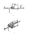
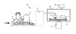
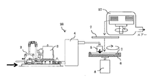
[11]本発明は、気体及び液体をそれぞれ吸引する手段と、前記気体及び前記液体を同時に加圧して搬送する手段と、該搬送された前記気体を含む前記液体を新たな気体と混合させることによって溶存気体を富化させるための気液混合槽と、該加熱装置によって加熱された溶存液を用いてマイクロ・ナノバブルを発生させるために、空洞の筒、該筒の周方向に2以上の貫通小穴のそれぞれの開口部が前記筒の径方向断面と平行な同一平面上で対向するように配置された前記2以上の貫通小穴、及び前記筒の少なくとも片端部にマイクロ・ナノバブル吐出口を有し、前記貫通小穴は該貫通小穴の断面中心部を通る延長線のすべてが前記筒の中心で交差するように配置される噴射ノズルと、前記気体のマイクロ・ナノバブルを含有する処理液を、表面にレジスト膜が付着した被処理基板又は表面が金属化合物で汚染された被処理基板に噴射するために前記噴射ノズルに接続されたノズルヘッダーと、を有するマイクロ・ナノバブル発生装置を備え、さらに、被処理基板支持を支持するために前記ノズルヘッダーに対向して設けるホルダー、及び前記気体のマイクロ・ナノバブルを含有する処理液を30〜90℃に加熱するための加熱手段を備えることを特徴とするマイクロ・ナノバブルによる洗浄装置を提供する。
[12]本発明は、前記加熱装置が、前記気液混合槽から送出された直後の前記気液混合の状態にある溶存液を加熱するために備える加熱装置であることと特徴とする前記[11]に記載のマイクロ・ナノバブルによる洗浄装置を提供する。
[13]本発明は、前記加熱装置が、前記気液混合槽の底部及び側部の少なくとも何れかの場所にヒータとして具備されていることを特徴とする前記[12]に記載のマイクロ・ナノバブルによる洗浄装置を提供する。
[14]本発明は、前記[11]〜[13]の何れかに記載のマイクロ・ナノバブルによる洗浄装置が、さらに、前記非処理基板の上の水滴及び水分を乾燥させる乾燥手段を有することを特徴とするマイクロ・ナノバブルによる洗浄装置を提供する。
[15]本発明は、前記ホルダーが、前記被処理基板に超音波振動を与えることができる超音波発生装置と接続していることを特徴とする前記[11]〜[14]の何れかに記載のマイクロ・ナノバブルによる洗浄装置を提供する。
[16]本発明は、前記非処理基板を支持するホルダーと前記処理液を噴射するノズルヘッダーの近くに配置する電極との間に電圧を印加する電圧印加手段を有することを特徴とする前記[11]〜[14]の何れかに記載のマイクロ・ナノバブルによる洗浄装置を提供する。
[17]本発明は、前記加熱装置が、さらに、前記ノズルヘッダー及び前記ホルダーの少なくとも何れかを加熱するための加熱装置又は温風発生装置を具備することを特徴とする前記[11]〜[16]の何れかに記載のマイクロ・ナノバブルによる洗浄装置を提供する。
[18]本発明は、前記加熱装置が、さらに、前記ノズルヘッダー及び前記ホルダーを一つの部屋として囲み、前記部屋の内部を30〜90℃の温度に制御するための空調機を備えることを特徴とする前記[11]〜[17]の何れかに記載のマイクロ・ナノバブルによる洗浄装置を提供する。
[19]本発明は、前記加熱するときの温度が50〜85℃であることを特徴とする前記[11]〜[18]の何れかに記載のマイクロ・ナノバブルによる洗浄装置を提供する。That is, the constitution of the present invention is as follows.
[1] In the present invention, when a substrate to be treated with a resist film deposited on the substrate or a substrate to be treated with the surface contaminated with a metal or a metal compound is measured by an ice embedding method using a cryotransmission electron microscope Peeling of the resist film or the metal or metal compound by spraying a treatment liquid containing micro-nano bubbles of gas having an average particle diameter of 100 nm or less and kept at a temperature of 30 to 90 ° C. The present invention provides a micro / nano bubble cleaning method characterized by performing the removal of
[2] The present invention is characterized in that the micro-nano bubbles of the gas have an average particle size of 30 nm or less when measured by a cryo-transmission electron microscope by an ice embedding method. Provides a cleaning method by micro and nano bubbles.
[3] The present invention is characterized in that the micro / nano bubbles of the gas contained in the treatment liquid have a density of 10 8 or more per 1 ml as measured by a cryotransmission electron microscope by an ice embedding method. The washing | cleaning method by the micro nano bubble as described in said [1] or [2] is provided.
[4] In the present invention, the treatment liquid containing the gas micro / nano bubbles is a solution having a dissolved gas, from the outside of a cylinder having two or more through small holes in the circumferential direction, the pressure above atmospheric pressure through the small through holes. When jetted with water, the dissolved liquid jetted from the respective openings of the two or more small through holes disposed opposite to each other on the same plane parallel to the radial cross section of the cylinder is made water hammer to the center of the cylinder The processing method according to any one of the above [1] to [3], which is a processing solution containing gas micro / nano bubbles generated by causing collisions to concentrate. provide.
[5] The present invention is any of the above-mentioned [1] to [4], wherein the gas is ozone or oxygen, and the treatment liquid is pure water containing micro-nano bubbles of ozone or oxygen. Provided is a method for cleaning with the micro / nano bubbles described above.
[6] The present invention is any of the above-mentioned [1] to [5], wherein the gas is a gas containing at least one of carbon dioxide and hydrogen peroxide in addition to ozone or oxygen. Provided is a method of cleaning with the described micro / nano bubbles.
[7] The present invention includes the step of drying water droplets and moisture on the untreated substrate before spraying the treatment liquid, according to any one of the above [1] to [6]. Provide a micro-nano bubble cleaning method.
[8] The present invention is characterized in that the treatment liquid containing the micro-nano bubbles of the gas is ejected while applying ultrasonic vibration to the substrate to be treated which is the object to be cleaned. ] The cleaning method by the micro nano bubble in any one of-.
[9] The present invention is characterized in that a voltage is applied between the non-treated substrate and an electrode disposed near a nozzle header for jetting the treatment liquid. The present invention provides a method of cleaning with micro / nano bubbles as described in
[10] The method according to any one of the above [1] to [9], wherein the temperature of the treatment liquid is more than 50 ° C. and 85 ° C. or less.
[11] The present invention is to mix means for sucking gas and liquid, means for simultaneously pressurizing and transporting the gas and liquid, and mixing the liquid containing the transported gas with a new gas. And a hollow cylinder, and two or more penetrations in the circumferential direction of the cylinder to generate micro / nano bubbles by using a gas-liquid mixing tank for enriching the dissolved gas by using the dissolved liquid heated by the heating device. The two or more through small holes disposed so as to face each other in the same plane parallel to the radial cross section of the cylinder, and the micro / nano bubble discharge port at at least one end of the cylinder. And the through small hole is a spray nozzle disposed so that all extension lines passing through the center of the cross section of the through small hole intersect at the center of the cylinder, and a treatment liquid containing the micro / nano bubbles of the gas. A micro / nano bubble generator having a nozzle header connected to the spray nozzle to spray a treated substrate having a resist film on its surface or a sprayed substrate on which the surface is contaminated with a metal compound; A holder provided opposite to the nozzle header for supporting the substrate to be processed, and a heating means for heating the processing solution containing the micro-nano bubbles of the gas to 30 to 90 ° C. To provide a cleaning device using micro / nano bubbles.
[12] The present invention is characterized in that the heating device is a heating device provided for heating the dissolved liquid in the state of the gas-liquid mixture immediately after being sent out from the gas-liquid mixing tank. 11] The cleaning apparatus by the micro nano bubble as described in 11] is provided.
[13] The present invention is characterized in that the heating device is provided as a heater at at least one of the bottom and the side of the gas-liquid mixing tank as the heater according to the above [12]. Provide a cleaning device according to
[14] The present invention provides that the micro / nano bubble cleaning apparatus according to any one of the above [11] to [13] further has a drying means for drying water droplets and moisture on the non-treated substrate. The present invention provides a micro / nano bubble cleaning apparatus characterized by the features.
[15] The present invention is characterized in that the holder is connected to an ultrasonic wave generator capable of applying ultrasonic vibration to the substrate to be treated. Provided is a micro / nano bubble cleaning apparatus as described.
[16] The present invention is characterized by comprising voltage application means for applying a voltage between the holder for supporting the non-treated substrate and the electrode disposed near the nozzle header for jetting the treatment liquid. [11] A cleaning apparatus using the micro / nano bubbles according to any one of [11] to [14].
[17] The present invention is characterized in that the heating device further comprises a heating device or a hot air generator for heating at least one of the nozzle header and the holder. The cleaning apparatus by the micro nano bubble in any one of 16] is provided.
[18] The present invention is characterized in that the heating device further includes an air conditioner for surrounding the nozzle header and the holder as one room and controlling the inside of the room to a temperature of 30 to 90 ° C. The washing | cleaning apparatus by the micro nano bubble in any one of said [11]-[17] is provided.
[19] The present invention provides the micro-nano bubble cleaning apparatus according to any one of the above [11] to [18], wherein the heating temperature is 50 to 85 ° C.
本発明による洗浄方法は、環境への負荷を低減しつつ、基板上のレジスト残渣付着の剥離若しくは金属又は金属化合物による汚染物の除去を、従来方法よりも効率的に、且つ、確実に行うことができる。さらに、被処理基板の乾燥、又は前記気体のマイクロ・ナノバブルを含む処理液を噴射するときに超音波振動を加えたり、若しくは電圧印加を行うことにより洗浄効果の一層の向上を図ることができる。 The cleaning method according to the present invention performs stripping of resist residue adhesion on a substrate or removal of metal or metal compound contamination more efficiently and reliably than the conventional method while reducing the load on the environment. Can. Furthermore, the cleaning effect can be further improved by applying ultrasonic vibration or applying a voltage when drying the substrate to be treated or spraying the treatment liquid containing the gas micro / nano bubbles.
本発明による洗浄装置は、従来のマイクロ・ナノバブル発生装置に、前記気体のマイクロ・ナノバブルの加熱するための装置、噴射ノズルを有するノズルヘッダー、及び前記被処理基板を支持するホルダーを組み合わるだけで、シンプルかつコンパクトな構成を有する洗浄装置を構築することができる。また、これらの装置構成に、乾燥手段、超音波発生装置、又は電圧印加手段を追加し具備させるだけで、洗浄時間の短縮化及び洗浄の効率化を図ることができる。 The cleaning apparatus according to the present invention can be achieved by simply combining a conventional micro / nano bubble generator with an apparatus for heating the gas micro / nano bubbles, a nozzle header having a jet nozzle, and a holder for supporting the substrate to be treated. It is possible to construct a cleaning device having a simple and compact configuration. Further, by adding a drying means, an ultrasonic wave generation device or a voltage application means to these apparatus configurations, the cleaning time can be shortened and the efficiency of the cleaning can be improved.
気体のマイクロ・ナノバブルの発生量は、洗浄用の処理液に含まれる気体の溶存量に依存しており、前記処理液の温度が高くなると液体に対する気体の溶解度定数が小さくするため、少なくなる傾向にある。そのため、気体のマイクロ・ナノバブルは高温で使用する場合は、洗浄能力の低下を招くと考えられており、今まで実施されていなかった。前記特許文献3にもマイクロ・ナノバブルの温度を15℃以上50℃以下とすることが記載されているように、気体のマイクロ・ナノバブルを含む溶液は、低めの温度で使用するのが一般的であった。また、前記特許文献1には、第1の剥離工程として、ナノバブルを混合させた第1の剥離液L1を40〜60℃程度の低温度で加熱することが記載されているが、これは、ナノバブルの状態でレジスト膜に対する高い浸透性を維持するために加熱されるものであると解するのが相当であり、気体のナノバブルを含む処理液を、被処理基板に直接的に噴射して、レジスト剥離を行う処理方法には適しない。
The generation amount of gas micro / nano bubbles depends on the dissolved amount of the gas contained in the treatment liquid for cleaning, and when the temperature of the treatment liquid becomes high, the solubility constant of the gas in the liquid tends to be small, so it tends to be small. It is in. Therefore, when used at high temperature, gas micro / nano bubbles are considered to cause a decrease in the cleaning ability, and have not been implemented until now. As described in
それに対して、本発明は、従来の一般常識にとらわれないで、洗浄として最適のマイクロ・ナノバブルの性状及び特性、並びに処理方法を詳細に検討した結果、気体のマイクロ・ナノバブルの粒径が従来よりも小さいことを利用し、気体のマイクロ・ナノバブルを含む処理液を高温にした状態で被処理基板に対して直接噴射する方法によって、レジスト膜の残渣付着物の剥離や金属又は金属化合物からなる汚染物の除去が従来方法に比べてより短時間で効率的に、且つ、確実にできることを見出してなされたものである。 On the other hand, as a result of examining in detail the properties and characteristics of the micro / nano bubbles and the processing method optimum for washing without being bound by the general common sense in the present invention, the particle size of the gas micro / nano bubbles Also, by peeling directly from the residual film on the resist film or contaminating the metal or metal compound by direct spraying the processing solution containing the gas micro / nano bubbles at a high temperature to the substrate to be treated. It has been found that the removal of material can be performed more efficiently and reliably in a shorter time than in the conventional method.
本発明において使用する処理液に含まれるマイクロ・ナノバブルの大きさは、平均粒径で規定することができる。平均粒径が小さいものほど、ナノレベルで含まれるバブルの量が多く、マイクロオーダーのバブルの量が少なくなる傾向にある。マイクロ・ナノバブルの大きさは、粒度分布(粒径の標準偏差)によっても影響を受けるが、その影響は小さく、処理液に含まれるマイクロ・ナノバブルは、平均粒径がナノレベルのオーダーであり、できるだけ小さい平均粒径を有することが必要である。 The size of the micro / nano bubbles contained in the treatment liquid used in the present invention can be defined by the average particle diameter. The smaller the average particle size, the more the amount of bubbles contained at the nano level, and the smaller the amount of micro-order bubbles tend to be. The size of the micro / nano bubble is also affected by the particle size distribution (standard deviation of particle size), but the effect is small, and the micro / nano bubble contained in the treatment liquid has an average particle size on the order of nano level, It is necessary to have an average particle size as small as possible.
本発明において、気体のマイクロ・ナノバブルは、氷包埋法によってクライオ透過型電子顕微鏡で測定したときの平均粒径が100nm以下であり、好ましくは30nm以下である。マイクロ・ナノバブルの平均粒径が100nm以下であるときに、剥離液の温度を高温で加熱した状態で噴射すると、レジスト膜の残渣付着物の剥離や金属又は金属化合物からなる汚染物の除去を、短時間に高い比率で確実に行うことができる。さらに、30nm以下であれば、著しく大きな効果を得ることができる。 In the present invention, the gas micro / nano bubbles have an average particle diameter of 100 nm or less, preferably 30 nm or less, as measured by a cryotransmission electron microscope by ice embedding method. When the average particle diameter of the micro / nano bubbles is 100 nm or less and the temperature of the stripping solution is jetted in a heated state at high temperature, stripping of residual deposits on the resist film and removal of contaminants consisting of metal or metal compound, It can be done reliably at a high rate in a short time. Furthermore, if it is 30 nm or less, a remarkable big effect can be acquired.
マイクロ・ナノバブルの粒径の測定方法としては、従来から様々な方法が知られている。それらの中で、ナノバブルの計測法は、光学的な観察が困難であるため、例えば、ミー散乱光を利用する光散乱法、レーザ回折・散乱法、液中のバブル粒子のブラウン運動を観測するナノ粒子トラッキング解析法、細孔電気抵抗法(コール・カウンター法)、動的光散乱法、MEMS(Micro Electro−Mechanical Systems)の梁を利用する共振式質量測定法等が提案されている。これらの方法以外にも、ゼータ電位測定によるナノバブルの粒子径を求める方法やスピントラップ剤を用いて電子スポン共鳴法(ESR)によるナノバブルの存在を確認する方法が提案されている。 Various methods are conventionally known as methods of measuring the particle size of micro / nano bubbles. Among them, since the measurement method of nanobubbles is difficult to optically observe, for example, a light scattering method using Mie scattered light, a laser diffraction / scattering method, and Brownian motion of bubble particles in liquid are observed. A nanoparticle tracking analysis method, a pore electrical resistance method (Cole-counter method), a dynamic light scattering method, a resonance type mass measurement method using a beam of MEMS (Micro Electro-Mechanical Systems), and the like have been proposed. Besides these methods, a method of determining the particle diameter of nanobubbles by zeta potential measurement and a method of confirming the presence of nanobubbles by electron spon resonance (ESR) using a spin trapping agent have been proposed.
本発明等は、上記以外のマイクロ・ナノバブル計測法として、氷包埋法によってクライオ透過型電子顕微鏡で測定する方法を提案している(特願2014−230407号を参照)。この方法は、液体を非晶質の固相状態にし、前記非晶質の固相状態にある液体に含まれる超微細バブルを透過型電子顕微鏡を用いて観察することによって、液中に含まれる超微細バブル及びその分布状態を直接的に画像として観測し解析できる。そのため、10μm未満の粒径を有する超微細バブルを高精度に測定することができる。本発明において規定する気体のマイクロ・ナノバブルの平均粒径は、この方法で測定して求めたものである。 The present invention etc. propose a method of measuring with a cryo transmission electron microscope by ice embedding method as micro / nano bubble measurement methods other than the above (see Japanese Patent Application No. 2014-230407). This method is contained in a liquid by making the liquid into an amorphous solid state and observing the ultrafine bubbles contained in the liquid in the amorphous solid state using a transmission electron microscope. The hyperfine bubbles and their distribution can be directly observed and analyzed as an image. Therefore, ultrafine bubbles having a particle size of less than 10 μm can be measured with high accuracy. The average particle diameter of the gas micro-nano bubbles specified in the present invention is determined by measurement using this method.
氷包埋法によってクライオ透過型電子顕微鏡で測定する方法は、マイクログリッド又はマイクロメッシュに保持した液体を試料として用い、エネルギーが10〜300キロエレクトロンボルト(keV)の透過型電子顕微鏡によって、観察のときに用いる電子線の数を1〜105電子/Å2に設定して測定が行われる。The method of measuring with a cryo-transmission electron microscope by ice embedding method uses a liquid held on a micro grid or a micro mesh as a sample and observes it by a transmission electron microscope with an energy of 10 to 300 kiloelectron volts (keV). The measurement is performed by setting the number of electron beams used sometimes to 1 to 10 5 electrons / Å 2 .
本発明で使用する処理液の温度は、剥離又は除去の洗浄効果、洗浄工程時の試料の取扱い、温度の管理、洗浄装置の能力と耐久性、省エネルギー、環境への負荷、及び安全性の観点から、室温以上100℃未満で最適化する必要がある。特に、本発明においては、環境への負荷を低減するため、処理液として純水を使用するのが好ましい。そこで、処理液の温度は、水の沸点以下である30〜90℃の範囲に設定する必要があり、好ましくは50〜85℃の範囲である。処理系の温度が30℃未満では、平均粒径が100nm以下である気体のマイクロ・ナノバブルを含有する処理液を用いても、処理時間が長くなる傾向にあるため。本発明の効果が十分に得られない。処理液の温度を高くすると、レジスト膜の残渣付着物の剥離や金属又は金属化合物からなる汚染物の除去を短時間で、且つ、効率的に行うことができるが、90℃を超えると、温度の管理が難しくなる。また、90℃を超える場合は、処理液の揮発とともにマイクロ・ナノバブルの解放速度が速くなるため、剥離又は除去効果が飽和する傾向にあるだけで、処理液の温度をより高温にする利点が失われる。処理液の温度が50〜85℃の範囲に設定するときに、高い洗浄効果を安定的に得ることができる。 The temperature of the treatment liquid used in the present invention is the washing effect of peeling or removal, handling of the sample during washing process, temperature control, ability and durability of washing apparatus, energy saving, environmental load, and safety point of view Therefore, it is necessary to optimize at room temperature or more and less than 100 ° C. In particular, in the present invention, it is preferable to use pure water as the processing solution in order to reduce the load on the environment. Therefore, the temperature of the treatment liquid needs to be set in the range of 30 to 90 ° C., which is lower than the boiling point of water, and preferably in the range of 50 to 85 ° C. If the temperature of the treatment system is less than 30 ° C., the treatment time tends to be long even when using a treatment liquid containing micro-nano bubbles of a gas having an average particle diameter of 100 nm or less. The effects of the present invention can not be sufficiently obtained. When the temperature of the processing solution is raised, peeling off of residual deposits on the resist film and removal of contaminants consisting of metal or metal compound can be performed in a short time and efficiently, but if it exceeds 90 ° C., the temperature Management becomes difficult. When the temperature exceeds 90 ° C., the release rate of the micro-nano bubbles increases with volatilization of the treatment liquid, so that the peeling or removal effect tends to saturate, and the advantage of making the temperature of the treatment liquid higher is lost. It will be. When the temperature of the treatment liquid is set in the range of 50 to 85 ° C., a high cleaning effect can be stably obtained.
本発明においては、マイクロ・ナノバブルの平均粒径だけでなく、処理液1ml中に含まれる個数、すなわち、マイクロ・ナノバブルの密度を高い値に規定することによって、高い洗浄効果を達成することができる。本発明で使用する処理液に含まれるマイクロ・ナノバブルの密度は、氷包埋法によってクライオ透過型電子顕微鏡で測定したときの密度が処理液1mlあたり108個以上であることが必要であり、好ましくは1012個/ml以上、より好ましくは1016個/ml以上である。本発明で利用するマイクロ・ナノバブルは、そもそも平均粒径が非常に小さいため、その密度が108個未満であると、バブル中に含まれる気体の濃度が薄くなるため、レジスト膜の残渣付着物の剥離や金属又は金属化合物からなる汚染物の除去を十分に行うことができない。例えば、気体として洗浄効果の高いオゾンを使用する場合、オゾン濃度が高いほど大きな洗浄効果が得られるが、マイクロ・ナノバブルの密度が108個未満であると、処理液に含まれるオゾン濃度が少なくなり、洗浄効果が限定的になる。In the present invention, a high cleaning effect can be achieved by specifying not only the average particle diameter of the micro / nano bubbles but also the number contained in 1 ml of the treatment liquid, that is, the density of the micro / nano bubbles to a high value. . The density of the micro / nano bubbles contained in the treatment liquid used in the present invention needs to be 10 8 or more per 1 ml of the treatment liquid, as measured by a cryotransmission electron microscope by ice embedding method. Preferably it is 10 12 cells / ml or more, more preferably 10 16 cells / ml or more. The micro / nano bubbles used in the present invention have an extremely small average particle diameter, and if the density is less than 10 8 , the concentration of the gas contained in the bubbles becomes low, so residue deposits on the resist film And removal of contaminants consisting of metals or metal compounds. For example, when ozone having high cleaning effect is used as gas, the higher the ozone concentration, the greater the cleaning effect can be obtained, but if the density of the micro / nano bubbles is less than 10 8 , the ozone concentration contained in the treatment liquid is small. And the cleaning effect is limited.
本発明で使用する気体のマイクロ・ナノバブルと処理液との組合せとしては、前記気体がオゾン又は酸素であり、前記処理液が、オゾン又は酸素のマイクロ・ナノバブルを含有する純水であることが好ましい。オゾンと純水、又は酸素と純水の組合せによって、環境への負荷の低減及び洗浄工程の簡略化と高効率化の両者を実現でき、且つ、高い洗浄効果を得ることができる。その中で、オゾンと純水の組合せによるオゾンマイクロ・ナノバブルが、洗浄効果の一層の向上を図ることができるため、より好ましい。 As a combination of gas micro / nano bubbles and treatment liquid used in the present invention, it is preferable that the gas is ozone or oxygen, and the treatment liquid is pure water containing ozone or oxygen micro / nano bubbles. . By the combination of ozone and pure water, or oxygen and pure water, it is possible to realize both reduction of environmental load, simplification of the cleaning process and high efficiency, and a high cleaning effect. Among them, ozone micro / nano bubbles by a combination of ozone and pure water are more preferable because they can further improve the cleaning effect.
本発明で使用する気体のマイクロ・ナノバブルは、前記気体が少なくともオゾン又は酸素であり、さらに、二酸化炭素及び過酸化水素の少なくとも何れかを含むことが好ましい。例えば、前記気体としてオゾン又は酸素と二酸化炭素とを含む処理液は、被処理基板上の付着物又は汚染物に二酸化炭素が吸着することに起因するオゾン又は酸素の洗浄物への誘導及び二酸化炭素の酸性化作用によって、より効率的な洗浄を行うことができる。また、オゾン又は酸素と過酸化水素とを含む場合は、酸素又はオゾンと過酸化水素との反応によりヒドロキシルラジカル(OH・)が生成する場合があり、このヒドロキシルラジカルの強い酸化力を利用することができる。その中で、特に、オゾンと二酸化炭素を組み合わせて作製する気体のマイクロ・ナノバブルは、取扱いが容易であるだけでなく、従来の方法と比べて非常に大きな効果が得られることが分かった。 The gas micro / nano bubbles used in the present invention are preferably such that the gas is at least ozone or oxygen, and further contains at least one of carbon dioxide and hydrogen peroxide. For example, a treatment liquid containing ozone or oxygen and carbon dioxide as the gas may induce ozone or oxygen to be cleaned due to adsorption of carbon dioxide on deposits or contaminants on the substrate to be treated, and carbon dioxide The acidifying action of can provide more efficient cleaning. Moreover, when ozone or oxygen and hydrogen peroxide are contained, hydroxyl radicals (OH.) May be generated by the reaction of oxygen or ozone and hydrogen peroxide, and the strong oxidizing power of this hydroxyl radical should be used. Can. Among them, it has been found that, in particular, gas micro-nano bubbles produced by combining ozone and carbon dioxide are not only easy to handle, but also extremely large effects can be obtained as compared with the conventional method.
以上のように、本発明の洗浄方法は、気体のマイクロ・ナノバブルを有する処理液の噴射により洗浄効果を高めることができるが、次に示す3つの方法を組合わせることにより、洗浄スピードを高め、洗浄時間の時間短縮及び洗浄効率の大幅な向上を図ることができる。 As described above, the cleaning method of the present invention can enhance the cleaning effect by jetting the processing solution having gas micro / nano bubbles, but can increase the cleaning speed by combining the following three methods: The time for cleaning can be shortened and the cleaning efficiency can be greatly improved.
まず、第1の方法として、前記気体のマイクロ・ナノバブルを有する処理液を噴霧する前に、前記非処理基板の上の水滴及び水分を乾燥させる工程を採用することが好適である。仮に、前記非処理基板の上に水滴及び水分が残存する場合は、前記気体のマイクロ・ナノバブルを有する処理液を噴射しても、残存する水が気体のマイクロ・ナノバブルの密度を低下させるため、洗浄効果の低下を招くことがある。また、マイクロ・ナノバブルは、粒子表面にゼータ電位を有し、周囲がOH−の負電荷によって囲まれていることが知られている。詳細は不明であるが、このOH−が様々な反応を経由して被処理基板上の付着物又は汚染物の分解除去を促進する成分であると考えられる。しかしながら、前記非処理基板の上に残存する水は、OH−イオンが前記付着物又は汚染物に接近し作用するときの障壁として働き、OH−イオンを利用した洗浄作用を弱めることが考えられる。したがって、前記非処理基板の上の水滴及び水分を乾燥させる工程を採用し、気体のマイクロ・ナノバブルの効果を阻害する要因をできるだけ排除することにより、洗浄効果の向上を図ることができる。First, as the first method, it is preferable to adopt a step of drying water droplets and moisture on the untreated substrate before spraying the treatment liquid having the gas micro / nano bubbles. If water droplets and moisture remain on the non-treated substrate, the remaining water lowers the density of the gas micro-nano bubbles even if the treatment liquid having the gas micro-nano bubbles is jetted. It may cause a decrease in the cleaning effect. In addition, it is known that micro / nano bubbles have a zeta potential on the particle surface, and the periphery is surrounded by an OH − negative charge. Although the details are unknown, it is believed that this OH − is a component that promotes the decomposition and removal of deposits or contaminants on the substrate to be treated via various reactions. However, the water remaining on the untreated substrate, OH - ions act as a barrier when acting close to the deposits or contaminants, OH - is conceivable to attenuate cleaning action using ion. Therefore, the cleaning effect can be improved by adopting the step of drying the water droplets and moisture on the non-treated substrate and eliminating as much as possible the factors that inhibit the effects of the gas micro / nano bubbles.
上記の乾燥工程は、例えば、通常の半導体ウエハの洗浄工程で使用されるスピンドライヤー、イソプロパノール(IPA)蒸気乾燥装置、スピンエッチェー等の乾燥手段を利用して行うことができる。スピンドライヤーとは、回転による遠心力とULPAフィルタ等のフィルタを介して吸引される清浄なエアの流れにより被処理基板をクリーンに水切りして水滴及び水分を乾燥させる装置である。また、前記乾燥工程の簡略化を図る場合は、気体のマイクロ・ナノバブル噴射する前に、ホルダーに据付けた被処理基板をあらかじめ高速回転させ、遠心力を利用しながら水滴及び水分を除去する方法を採用することができる。その場合、高速回転中に乾燥エア又は高温エア(エアの代わりに、不活性ガスである窒素ガスを使用することもできる。)を前記被処理基板に吹き付けることにより、水滴及び水分を除去する方法を採用してもよい。さらに、水滴及び水分の乾燥を速めるため、アルコール等の揮発性の高い液体又は該揮発性液体を含む水を被処理基板に噴霧してもよい。これらの乾燥工程は、本発明の洗浄方法で構築する一連の工程の一つの工程として組み入れることができるが、バッチ式の分離した工程で行ってもよい。 The above-mentioned drying step can be performed using, for example, a drying means such as a spin drier, an isopropanol (IPA) vapor drying device, or a spin etcher used in a general semiconductor wafer cleaning step. A spin drier is a device for draining a substrate to be cleaned cleanly to dry water droplets and moisture by centrifugal force due to rotation and the flow of clean air drawn through a filter such as a ULPA filter. In addition, in order to simplify the drying process, a method of removing water droplets and moisture while using a centrifugal force by rotating a substrate to be processed installed in a holder at high speed in advance before injecting micro and nano bubbles of gas It can be adopted. In that case, a method of removing water droplets and moisture by blowing dry air or high temperature air (in place of air, nitrogen gas which is an inert gas may be used) to the substrate during high speed rotation. May be adopted. Furthermore, in order to accelerate the drying of water droplets and moisture, a highly volatile liquid such as alcohol or water containing the volatile liquid may be sprayed onto the substrate to be processed. These drying steps can be incorporated as one step of a series of steps constructed by the washing method of the present invention, but may be performed in batch-wise separated steps.
本発明においては、洗浄効果を上げるための第2の方法として、洗浄対象物である基板に超音波振動を与えることが、前記基板からレジスト膜の残渣付着物の剥離、又は金属又は金属化合物からなる汚染物の除去に対して大きな効果を得ることができる。そのメカニズムは詳細には不明であるが、超音波振動は、前記処理液に含まれる微細粒径で、壊れにくいマイクロ・ナノバブルの均一な崩壊を助け、マイクロ・ナノバブル中に存在する気体、例えば、オゾンの解放を助長する機能を有するのではないかと考えられる。すなわち、本発明の洗浄方法においては、前記処理液が30〜90℃、好ましくは50〜85℃の高温に保持されても、マイクロ・ナノバブルは超微細の粒径を有するため前記処理液中に留まっている。そのマイクロ・ナノバブルが被処理基板への噴射によって被処理基板上で開放されるときに、超音波振動を与えることによってマイクロ・ナノバブル中の気体の開放が、均一に、且つ微小空間又は微小空隙にまで実現できるため、洗浄効果に大きく寄与するものと考えている。 In the present invention, as a second method for enhancing the cleaning effect, ultrasonic vibration may be applied to the substrate to be cleaned, peeling of residue deposits on the resist film from the substrate, or metal or metal compound. Can have a great effect on the removal of contaminants. Although the mechanism is not known in detail, ultrasonic vibration helps uniform collapse of micro-nano bubbles which are hard to break with the fine particle size contained in the treatment solution, and gases present in micro-nano bubbles, for example, It is thought that it has a function to promote the release of ozone. That is, in the cleaning method of the present invention, even if the treatment liquid is maintained at a high temperature of 30 to 90 ° C., preferably 50 to 85 ° C., the micro / nano bubbles have an ultrafine particle diameter and thus in the treatment liquid. It has stayed. When the micro / nano bubbles are released on the treated substrate by injection onto the treated substrate, the release of the gas in the micro / nano bubbles is uniformly applied to the minute space or the minute space by applying ultrasonic vibration. It can be realized to a great extent, and we believe it will greatly contribute to the cleaning effect.
前記超音波振動を印加するときの振動周波数は10kHz〜3MHzであれば、本発明の効果を十分に奏することができる。ただし、振動周波数が高い場合は、被処理基板の欠け、割れ、又は損傷が見られ、悪影響を及ぼす場合があるため、振動週者数は10kHz〜1MHzがより好ましい。 If the vibration frequency when applying the ultrasonic vibration is 10 kHz to 3 MHz, the effects of the present invention can be sufficiently achieved. However, when the vibration frequency is high, chipping, cracking or damage of the substrate to be treated may be observed, which may adversely affect the number of vibration weeks is preferably 10 kHz to 1 MHz.
また、洗浄効果を上げるための第3の方法として、前記非処理基板と前記処理液を噴射するノズルヘッダーの近くに配置する電極との間に電圧を印加することによって、前記非処理基板からレジスト膜の残渣付着物の剥離、又は金属又は金属化合物からなる汚染物の除去に対して大きな効果を得ることができることが分かった。この方法は、前記処理液を噴射するノズルヘッダーの近くに電極を配置し、その電極と前記非処理基板との間に直流電源又はパルス電源等により連続的な直流電圧又はパルス状の電圧を印加しながら、マイクロ・ナノバブルを被処理基板へ噴射を行うものであり、洗浄効果の向上に対して相乗的な役割を担うという新たな知見に基づいてなされたものである。処理液に含まれるマイクロ・ナノバブルは表面にOH−イオンが存在するため、電圧印加により電気分解と似た現象で、壊れにくい微細粒径を有するマイクロ・ナノバブルの崩壊を促進する可能性がある。それにより、前記マイクロ・ナノバブル中に存在する気体、例えば、オゾン及び二酸化炭素等の解放が助長されるとも考えられるが、詳細は不明である。Further, as a third method for enhancing the cleaning effect, a voltage is applied between the non-treated substrate and the electrode disposed near the nozzle header for jetting the treatment liquid, whereby the resist from the non-treated substrate is removed. It has been found that a great effect can be obtained on the removal of residual deposits on the film or on the removal of contaminants consisting of metals or metal compounds. In this method, an electrode is disposed near a nozzle header for injecting the processing solution, and a continuous DC voltage or pulse voltage is applied between the electrode and the untreated substrate by a DC power supply or a pulse power supply. However, the micro / nano bubbles are jetted onto the substrate to be treated, and they are made based on the new finding that they play a synergistic role in improving the cleaning effect. Since micro-nano bubbles contained in the treatment liquid have OH - ions on the surface, they may accelerate the collapse of micro-nano bubbles having a fine particle size which is hard to break by a phenomenon similar to electrolysis by voltage application. It is also considered that this promotes the release of the gas present in the micro / nano bubbles, such as ozone and carbon dioxide, but the details are unknown.
この方法を利用するときは、電圧印加を被処理基板へ直に行うよりも、前記非処理基板を支持するホルダーを用いて、前記ホルダーと前記ノズルヘッダーの近くに配置する電極との間で行うことが操作を容易に行うことができ、また、安全性の点からも実用的である。また、印加電圧としては、高電圧が容易に得られること、エネルギー効率が高いこと等の理由から、直流電圧よりもパルス電圧を使用することが好ましい。 When using this method, rather than applying voltage directly to the substrate to be treated, using a holder that supports the untreated substrate, it is performed between the holder and an electrode placed near the nozzle header It is easy to operate and is also practical in terms of safety. In addition, as the applied voltage, it is preferable to use a pulse voltage rather than a DC voltage because high voltage can be easily obtained, energy efficiency is high, and the like.
上記のように、電圧を印加しながら気体のマイクロ・ナノバブルによって洗浄を行うとき、非処理基板として回路パターン形成後の半導体ウエハを使用する場合は、電圧印加がウエハから得られる半導体素子の電気的な誤動作等の要因となり、悪影響を及ぼすことがある。その場合は、例えば、イオナイザー発生装置等によって電荷を打ち消すようなイオンを前記処理基板の裏側から常時発射し、ウエハに対して電圧印加による悪影響を低減する方法を採用してもよい。一方、回路パターンが形成される前のウエハの洗浄に適用する場合は、そのような悪影響を考慮する必要がないため、非常に大きな洗浄効果が得られる。 As described above, when cleaning is performed with gas micro / nano bubbles while applying a voltage, when using a semiconductor wafer after circuit pattern formation as an untreated substrate, the electrical application of the semiconductor element whose voltage application can be obtained from the wafer Cause a malfunction or other adverse effects. In such a case, for example, a method may be employed in which ions that can cancel charges by an ionizer generator or the like are constantly emitted from the back side of the processing substrate to reduce the adverse effect of voltage application to the wafer. On the other hand, when applied to the cleaning of the wafer before the circuit pattern is formed, it is not necessary to consider such an adverse effect, and a very large cleaning effect can be obtained.
本発明においては、前記処理液の温度を30〜90℃、好ましくは50〜85℃の状態で、洗浄対象物である被処理基板に噴射するとき、前記被処理基板を回転することによって、均一な洗浄を行うことができる。 In the present invention, when the temperature of the processing liquid is 30 to 90 ° C., preferably 50 to 85 ° C., when the substrate to be processed is sprayed, the substrate to be processed is uniformly rotated. Can be performed.
次に、本発明の洗浄方法を実施するための洗浄装置について図面を用いて説明する。 Next, a cleaning apparatus for carrying out the cleaning method of the present invention will be described using the drawings.
図1は本発明のマイクロ・ナノバブルによる洗浄装置の一例を示す図であり、図1において(a)及び(b)は、それぞれ洗浄装置の正面図及び斜視図である。図1に示す洗浄装置1は、ベローズポンプ2、気液混合槽3、加熱装置4及び不図示のマイクロ・ナノバブル発生ノズルを有するマイクロ・ナノバブル手段とからなり、気体のマイクロ・ナノバブルを含有する処理液を噴射するための不図示の噴射ノズルを有するノズルヘッダー5から構成される。加熱装置4によって加熱された処理液は、ノズルヘッダー5からホルダー6に支持された被処理基板7に向けて噴射され、マイクロ・ナノバブルを発生させ洗浄を行う。被処理基板7を支持するホルダー6は、回転機構を有する回転台を兼ねている。また、ホルダー6は、超音波発信装置8と接続されており、必要に応じて、被処理基板7に超音波を印加できるような機構になっている。
FIG. 1 is a view showing an example of the cleaning apparatus using micro / nano bubbles of the present invention, and in FIG. 1, (a) and (b) are a front view and a perspective view of the cleaning apparatus, respectively. The cleaning apparatus 1 shown in FIG. 1 comprises a
図1に示す洗浄装置に具備されるマイクロ・ナノバブル発生装置の部分だけを抜き出して、図2に装置構成を示す。図2において、(a)及び(b)はそれぞれマイクロ・ナノバブル発生装置の正面図と斜視図である。図2において、2がベローズシリンダポンプ、9がポンプコントローラ、3が気液混合槽、10が圧力センサ、11がマイクロ・ナノバルブ発生用ノズル取付部、12が液吸引管、13が気体吸引口、14が気体吸引調整バルブである。 Only the portion of the micro / nano bubble generator included in the cleaning apparatus shown in FIG. 1 is extracted, and the apparatus configuration is shown in FIG. In FIG. 2, (a) and (b) are respectively a front view and a perspective view of a micro / nano bubble generating device. In FIG. 2, 2 is a bellows cylinder pump, 9 is a pump controller, 3 is a gas-liquid mixing tank, 10 is a pressure sensor, 11 is a micro / nano valve generating nozzle attachment, 12 is a liquid suction pipe, 13 is a gas suction port, 14 is a gas suction control valve.
これらは、図2の(b)に示す斜視図のように配置する。2の接液部をフッ素樹脂で作成したベローズシリンダポンプ2で12の液吸引管、14の気体吸引調整バルブを使用して気体量を調整してポンプ内部に液と気体を混ぜた状態で吸い込んでベローズ内部で撹拌、溶存させて、圧縮し液の中に気体を溶存させる。本発明においては、ベローズシリンダポンプ2はメタルフリーであれば良く、フッ素樹脂以外のプラスチック、例えば、ポリエチレン、ポリプロピレン及びポリエチレンテレフタレート等の汎用プラスチック、ポリアセタール、ポリアミド、ポリカーボネート及び変性ポリフェニレンエーテル等のエンジニアリングプラスチック、ポリエーテルサルフォン、ポリフェニレンスルフィド、ポリエーテルエーテルケトン及び液晶ポリマー等のスーパーエンジニアリング等の少なくとも1種を使用しても良い。その場合、ポンプだけでなく、液設部にもフッ素樹脂を始め、前記の各種プラスチックを用いることによって、信頼性の高い清浄なマイクロ・ナノバブル発生装置とすることができる。また、本発明において、厳密なメタルフリー化による洗浄や殺菌が要求されない場合には、上記のプラスチックだけでなく、金属やセラミックスを使用しても良い。
These are arranged as shown in the perspective view shown in FIG. The
次に、気液混合槽3に気体と液をポンプ2で撹拌して圧送する。ポンプ2は、主に圧縮空気起動式ベローズシリンダポンプを使用するが、電動式のものであっても良い。気液混合槽3の気体と液とは、ポンプ2からの圧力を受けており、気体が溶存しやすくなる。つまり気体と液体とをポンプ2から圧送する圧力を10の圧力センサでチェックしている。この方法によって溶存気体の量を多くしてマイクロ・ナノバブルの発生量を増やす準備を行う。本発明のマイクロ・ナノバルブ発生システムはポンプ2としてベローズシリンダポンプを用いるのが実用的であるが、用途に応じて、従来から送液ポンプとして公知のピストンポンプ、プランジャーポンプ又はダイヤフラム等の往復動ポンプや、ギヤーポンプ、偏心ポンプ又はネジポンプ、カスケードポンプ、ベーンポンプ等の回転ポンプ等を適用することができる。
Next, the gas and liquid are stirred into the gas-
圧送されて気液混合槽3に入った液は気体と混合して、気体を液の内部に溶存させてからマイクロ・ナノバルブ発生用ノズル取り付け部11に送る。マイクロ・ナノバルブ発生用ノズル取り付け部11は、溶存した気体を直径が100μm以下、好ましくは30μm以下の大きさのマイクロ・ナノバルブを大量に作成するノズルと接続する部分である。
The liquid that is pumped and enters the gas-
このとき、10の圧力センサでノズル11と気液混合槽2との間の液圧力の変動をみて気液の溶存状態を監視する。こうすることで安定したマイクロ・ナノバルブ用発生ノズルに必要な一定した圧力状態を実現する。
At this time, the
図2の(a)及び(b)に示す本発明で使用するマイクロ・ナノバルブ発生装置を用いて実施する工程は次の通りである。液吸引管12、気体吸引口13及び気体吸引調整バブル14を用いて行うのが気体・液体吸引工程である。圧力は、圧力センサ10で調整する。次に、ベローズシリンダポンプ2を用いて気体を含む液体を加圧する工程が気体・液体加圧工程である。引き続き、加圧された前記の気体を含む液体を新たな気体と混合させるために、ポンプコントローラ9及び気液混合槽3を用いて行う工程が溶存気体富化工程である。その後、後述する本発明の発生ノズルをマイクロ・ナノバルブ発生用ノズル取付部11に接続してからマイクロ・ナノバブルを発生させる。この工程を溶存気体微細化工程と呼ぶが、マイクロ・ナノバブルは、2以上の貫通小穴を有する筒の外部から該貫通小穴を通して大気圧以上の圧力で噴射し、前記筒の内部の一点で衝突させることによって発生させることができる。
The steps performed using the micro-nano valve generator used in the present invention shown in (a) and (b) of FIG. 2 are as follows. What is performed using the
図3に、図1の洗浄装置において気体のマイクロ・ナノバブルを発生させるノズル形状及び処理液を噴射するノズルヘッダーの例をそれぞれ示す。図3において、(a)及び(b)は、それぞれノズルヘッダー5の断面図及び上面図である。図3の(a)は、(b)のD−D断面を示している。
FIG. 3 shows an example of a nozzle shape for generating gas micro / nano bubbles in the cleaning apparatus of FIG. 1 and an example of a nozzle header for ejecting a processing solution. In FIG. 3, (a) and (b) are a sectional view and a top view of the
図3の(a)及び(b)に示すように、ノズルヘッダー5は、処理液を噴射するための噴射ノズル15及びマイクロ・ナノバブル吐出ノズル16と台17とから構成されており、液衝突ノズル16の1個又は2個以上を17の台上に取り付け配置する。ここで、液衝突ノズル16が、気体のマイクロ・ナノバブルを発生させるノズル形状の例である。液衝突ノズル16から噴射した処理液(Q)は、噴射ノズル15の噴射口15aから被処理基板7に向って噴射されて洗浄が行われる。本発明においては、処理液の温度を30〜90℃、好ましくは50〜85℃に調整するが、この温度の調整はノズルヘッダー5の部分を通過する処理液で行うことが好ましい。洗浄能力とノズルヘッダー5の部分を通過する処理液の温度との相関性が良いからである。そのため、ノズルヘッダー5には、処理液の温度を測定するための温度センサーを設けることが好ましい。
As shown in (a) and (b) of FIG. 3, the
また、図4は、図3の(a)に示すノズルヘッダー5の液衝突ノズル16を配置した部分の拡大図である。図4に示すように、16の液衝突ノズルの1個の形状において、16aの小さな穴は16の中心に向かって空いている。この小さな穴16aを通り、高圧で入った液を液衝突ノズル16の中心部分で衝突させてマイクロ・ナノバブルを発生させ、矢印Qで示す方向に噴射する。実験の結果、液の速度Vをコントロールすれば、発生したマイクロ・ナノバブルの量が多く、かつバブルの寿命が長くなることがわかった。速度Vの目安として、25m/秒を超える速度になると安定したマイクロ・ナノバブル発生ノズルになる。
4 is an enlarged view of a portion where the
図5は、本発明のマイクロ・ナノバブルによる洗浄装置において、加熱手段の変形例を示す図である。図5に示す洗浄装置18は、図1に示す加熱装置4が気液混合槽3の下流側に配置されておらず、気液混合槽3の底部に加熱手段としてヒータ19が設置されており、加熱手段が気液混合槽3の下流側に配置されている点で、図1に示す洗浄装置1とは構成が異なる。ヒータ19を設ける位置は気液混合槽3の底部に限定されず、気液混合槽3の側部に設けてもよい。また、気液混合槽3の底部及び側部の両方に設けることもできる。
FIG. 5 is a view showing a modification of the heating means in the micro / nano bubble cleaning apparatus of the present invention. In the
図6は、本発明のマイクロ・ナノバブルによる洗浄装置において、加熱手段の別の変形例を示す図である。図6に示す洗浄装置20は、気液混合槽3とノズルヘッダー5とを接続する配管がリボンヒータ21で加熱され、また、ノズルヘッダー5が温風ヒータ22で加熱される。この方式を採用しても、処理液の温度を所定の温度範囲に設定することができる。図6に示す装置は、リボンヒータ21及び温風ヒータ22の両者を有するが、両者のどちらかを設置する方式でもよい。
FIG. 6 is a view showing another modified example of the heating means in the micro / nano bubble cleaning apparatus of the present invention. In the
図7は、本発明のマイクロ・ナノバブルによる洗浄装置において、加熱手段のさらに別の変形例を示す図である。図7に示す洗浄装置23は、図1に示す装置に、さらにノズルヘッダー5及びホルダー6が含まれる空間を一つの部屋24として囲み、部屋23の内部を30〜90℃の温度に制御するための空調機25を備える。図7に示す洗浄装置は、処理液を所定の温度に調整することが容易であり、温度の制御が均一にできるという利点を有する。
FIG. 7 is a view showing still another modified example of the heating means in the micro / nano bubble cleaning apparatus of the present invention. In the
図8は、本発明のマイクロ・ナノバブルによる洗浄装置において、被処理基板の乾燥手段を備える装置例を示す図である。図8に示す洗浄装置26は、図1に示す洗浄装置に、半導体ウエハ等の被処理基板上に残存する水滴及び水分を乾燥するための乾燥手段27を備える。乾燥手段27としては、上記で述べたように、スピンドライヤー、イソプロパノール(IPA)蒸気乾燥装置、スピンエッチェー等を使用できるが、図8にはスピンドライヤーの例を示している。洗浄装置26において、まず、ウエハ等の被処理基板7を乾燥手段27に挿入し、環境エアを取り込む遠心力+吸気乾燥方式で乾燥を行う。その後、図中の点線矢印に示すように乾燥後の被処理基板7を取出して回転機構を有するホルダー6に支持し、不図示の噴射ノズルを有するノズルヘッダー5から気体のマイクロ・ナノバブルを有する処理液を回転している被処理基板7に向けて、図中の↓で示すように噴射する。
FIG. 8 is a view showing an example of the apparatus for cleaning with a micro / nano bubble according to the present invention, which is provided with a drying means of a substrate to be processed. The
図9は、本発明のマイクロ・ナノバブルによる洗浄装置において、被処理基板の電圧印加手段31を備える装置例を示す図である。電圧印加手段31は、基本的に、処理液を噴射するノズルヘッダー5の近くに配置される電極29と、電源30と、電極29及び被処理基板7を支持するホルダー6を電源30に接続する電気配線とから構成され、図1に示す洗浄装置に追加される装置及び部品である。図9に示す洗浄装置28において、電極29とホルダー6とは、それぞれ電源30の(+)側及び(−)側に電気的に接続される。気体のマイクロ・ナノバブルを有する処理液は、電源30によって電圧を印加しながら、図中の↓で示すように被処理基板7に向けて噴射され、前記非処理基板からレジスト膜の残渣付着物の剥離、又は金属又は金属化合物からなる汚染物の除去が行われる。電源6による印加電圧値の範囲としては特に制限はないが、10〜100Vの範囲にある直流電圧、又は電圧が10〜100Vで、10〜50kHzの周波数を有するパルス電圧を印加するのが実用的である。本発明においては、直流電圧に比べて、パルス電圧を使用することが好ましい。
FIG. 9 is a view showing an example of an apparatus provided with voltage application means 31 for a substrate to be processed in the cleaning apparatus using micro / nano bubbles of the present invention. The voltage application means 31 basically connects the
図1及び図5〜図7に示す洗浄装置は、従来のマイクロ・ナノバブル発生装置に、気体のマイクロ・ナノバブルを加熱するための装置、及び被処理基板に噴射するための噴射ノズルを有するノズルヘッダーと前記被処理基板を支持するホルダーとを付加するだけで、シンプルかつコンパクトな装置構成を構築することができる。また、図8及び図9に示す洗浄装置は、図1及び図5〜図7に示す洗浄装置に、それぞれ被処理基板の乾燥手段又は電圧印加手段を付属させることにより構成することができ、洗浄時間の短縮化及び洗浄の効率化を図る上で好適な装置とすることができる。 The cleaning apparatus shown in FIGS. 1 and 5 to 7 is a conventional micro / nano bubble generating apparatus, an apparatus for heating gas micro / nano bubbles, and a nozzle header having a jet nozzle for jetting onto a substrate to be treated A simple and compact device configuration can be constructed simply by adding a holder for supporting the substrate to be processed and the substrate to be processed. The cleaning apparatus shown in FIGS. 8 and 9 can be configured by attaching drying means or voltage application means to the substrate to be processed to the cleaning apparatus shown in FIGS. 1 and 5 to 7, respectively. An apparatus suitable for shortening the time and improving the efficiency of cleaning can be obtained.
以下において、本発明に基づく実施例を具体的に説明するが、本発明はこれらの実施例によって何ら限定されるものではない。 EXAMPLES Hereinafter, examples based on the present invention will be specifically described, but the present invention is not limited by these examples.
<実施例1>
前記特許文献4に開示された方法に従ってナノバブル水作製装置ΣPM-5(ベローズポンプ式) (シグマテクノロジー有限会社製)により空気ナノバブル水を作製し、純水によって100倍に希釈して測定用試料として用いた。また、参考用試料としてナノバブル作製前の純水を用いた。ナノバブル作製前の純水は、ナノバブルを含まない水に相当する。Example 1
According to the method disclosed in the
試料急速凍結装置Vitrobot Mark IV (FEI社製)により作製直後の前記空気ナノバブル水を急速凍結してナノバブルをアモルファス氷中に包埋した試料を作製し、観察用試料とした。試料厚さは200nmである。一方、ナノバブルを含まない水(純水)についても同じ試料急速凍結装置により急速凍結して参考用試料とした。試料厚さは200nmである。300keVの電子エネルギーを有するクライオ透過型電子顕微鏡Titan Krios (FEI社製)を用いて、試料温度約80Kにおいてアモルファス氷中に包埋されたナノバブルを直接観察した。観察に用いる電子線は、Low dose技術によって20 電子/Å2程度であり、撮影中の試料温度の上昇はほとんどなかった。
A sample rapid freezing apparatus Vitrobot Mark IV (manufactured by FEI) immediately freezes the air nanobubble water immediately after preparation to prepare a sample in which the nanobubbles are embedded in amorphous ice to prepare a sample for observation. The sample thickness is 200 nm. On the other hand, water (pure water) not containing nanobubbles was also rapidly frozen by the same sample rapid freezing apparatus and used as a reference sample. The sample thickness is 200 nm. Using a cryo-transmission electron microscope Titan Krios (manufactured by FEI) having an electron energy of 300 keV, nanobubbles embedded in amorphous ice were directly observed at a sample temperature of about 80K. The electron beam used for observation was about 20 electrons /
図10に、空気ナノバブルを含む純水を凍結したアモルファス氷及び純水(ナノバブルを含まない水)を凍結したアモルファス氷について電子顕微鏡像の写真を示す。また、空気ナノバブル水については、電子顕微鏡写真の下にバブルの粒度分布(サイズ分散を示すヒストグラム)を示す。 FIG. 10 shows photographs of electron microscopic images of amorphous ice frozen with pure water containing air nanobubbles and amorphous ice frozen with pure water (water not containing nanobubbles). In addition, for air nanobubble water, the particle size distribution of the bubble (a histogram indicating the size dispersion) is shown below the electron micrograph.
図10の左側に示す電子顕微鏡像の写真は、ΣPM−5によって作製後、ただちに観察された空気ナノバブルであり、写真中に観察される円形のコントラストがナノバブルである。画像処理の結果、平均粒径は7nmである。ヒストグラムの測定に用いたアモルファス氷の体積は3.2×10⁻¹⁴ cc(400 nm×400 nm×200 nm厚さ)であり、その中にバブルは約260個含まれている。100倍に希釈したナノバブル水を観察していることから、このナノバブル水の空気ナノバブルの濃度は、8.1×10¹⁷個/cc (ml)(81京個/cc (ml))であると評価される。それに対して、図10の右側に示す電子顕微鏡像の写真はアモルファス氷でありコントラストの変化はなく、バブルが含まれない水であることが確認できる。このように、本発明による測定方法及び測定装置によって、水に含まれるナノバブルの存在を直接的に画像として確認することができるだけでなく、ナノバブルの粒子径、個数、粒度分布及び形態に関する情報を取得することができる。The photograph of the electron microscope image shown on the left side of FIG. 10 is an air nanobubble observed immediately after preparation by PMPM-5, and a circular contrast observed in the photograph is a nanobubble. As a result of image processing, the average particle size is 7 nm. The volume of amorphous ice used for the measurement of the histogram is 3.2 × 10 -14 cc (400 nm × 400 nm × 200 nm thickness), in which about 260 bubbles are contained. The concentration of air nanobubbles in this nanobubble water is estimated to be 8.1 × 10 17 cells / cc (ml) (81 kyocograms / cc (ml)), since nanobubble water diluted 100 times is observed. Ru. On the other hand, it is possible to confirm that the photograph of the electron microscope image shown on the right side of FIG. 10 is amorphous ice, there is no change in contrast, and water is free of bubbles. Thus, not only the presence of nanobubbles contained in water can be directly confirmed as an image by the measurement method and apparatus according to the present invention, but also information on the particle size, number, particle size distribution and morphology of nanobubbles is obtained can do.
図10の左側に示す空気ナノバブルを含む純水を、図1に示す洗浄装置に適用して、半導体のウェハ基板上に付着している残渣レジスト膜の洗浄を行った。空気ナノバブルを含む純水は、瞬間的に加熱処理ができる加熱処理装置4によって約85℃まで温度を上げ、ノズルヘッダー5を通過する空気ナノバブルを含む純水の温度を70〜75℃に調整した。ここで、空気ナノバブルを含む純水の温度を一つの温度で厳密に設定することは量産性を考慮した場合に実用的でないため、調整温度の最低温度が本発明で使用する処理液で規定する加熱温度とみなすことができる。空気を溶存させ加熱処理した純水を、ノズルヘッダー5から発射してマイクロ・ナノバブルを発生させ洗浄を行う。このとき、洗浄対象物である半導体ウエハ基板は、ホルダー6を回転させて回転しながら洗浄を行った。その結果、常温でのマイクロ・ナノバブル発生装置では、レジスト膜の残渣を完全に剥離する時間が30分かかる洗浄を、70〜75℃の高温にすると15分以内と約1/2の時間でできることが分かった。
Pure water containing air nanobubbles shown on the left side of FIG. 10 was applied to the cleaning apparatus shown in FIG. 1 to clean the residual resist film deposited on the semiconductor wafer substrate. The temperature of pure water containing air nanobubbles was raised to about 85 ° C. by the
また、純水に溶存させる気体として、空気の代わりに、酸素を用いて、前記と同様の方法によって酸素ナノバブルを洗浄用処理液として使用した場合は、レジスト膜の残渣を完全に剥離する時間が10分となり、洗浄時間を1/3にまで短縮できることが確認できた。 When oxygen nanobubbles are used as the treatment liquid for cleaning by the same method as described above using oxygen instead of air as a gas to be dissolved in pure water, the time for completely removing the residue of the resist film It was 10 minutes, and it was confirmed that the cleaning time could be reduced to 1/3.
<実施例2>
前記特許文献4に開示された方法に従ってナノバブル水作製装置ΣPM-5 (べローズポンプ式) (シグマテクノロジー有限会社製)によりオゾンナノバブル水を作製した後、半月程度時間を経たオゾンナノバブルを純水によって100倍に希釈したものを測定試料として用いた。試料厚さは200nmである。この試料を実施例1と同じ試料急速凍結装置で急速凍結させた後、実施例1と同じクライオ透過型電子顕微によって試料温度約80Kにおいてアモルファス氷中に包埋されたナノバブルを直接観察した。観察に用いる電子線は、Low dose技術によって20電子/Å2程度であり、撮影中の試料温度の上昇はほとんどなかった。Example 2
After producing ozone nano bubble water by nano bubble water production device PMPM-5 (manufactured by Sigma Technology Co., Ltd.) (manufactured by Sigma Technology Co., Ltd.) according to the method disclosed in the
この試料を用いて観察した電子顕微鏡像の写真及びその写真の下にバブルの粒度分布(サイズ分散を示すヒストグラム)を図11に示す。図11に示す画像は、ΣPM−5によって作製後、半月程度経たオゾンナノバブルを観察したものである。平均粒径は18nmであり、図10に示す空気ナノバブルと比べてやや大きく、合体したことによりサイズの粗大化も起こっていると考えられる。ヒストグラムの測定に用いたアモルファス氷の体積は3.2×10⁻¹⁴ cc(400 nm×400 nm×200 nm厚さ)であり、その中にバブルは約21個含まれている。100倍に希釈したナノバブル水を観察していることから、このナノバブル水のオゾンナノバブルの濃度は、8.6×10¹⁶個/cc (ml)(約9京個/cc (ml))であると評価される。The photograph of the electron microscope image observed using this sample and the particle size distribution of the bubble (a histogram showing the size dispersion) are shown in FIG. 11 below the photograph. The image shown in FIG. 11 is an observation of an ozone nanobubble about half a month after preparation by PMPM-5. The average particle size is 18 nm, which is slightly larger than the air nanobubbles shown in FIG. 10, and it is considered that the coarsening of the size is also caused by the coalescence. The volume of amorphous ice used for the measurement of the histogram is 3.2 × 10 -14 cc (400 nm × 400 nm × 200 nm thickness), in which about 21 bubbles are contained. The concentration of ozone nanobubbles in this nanobubble water is estimated to be 8.6 × 10 16 cells / cc (ml) (about 9 kyocatures / cc (ml)) because 100% diluted nanobubble water is observed Be done.
図11に示すオゾンナノバブルを含む純水を、図1に示す洗浄装置に適用して、表面が金属又は金属化合物で汚染している半導体のウェハ基板4枚を用いて、金属又は金属化合物による汚染物の洗浄を行った。オゾンナノバブルを含む純水は、瞬間的に加熱処理ができる加熱処理装置4によって約80℃まで温度を上げ、ノズルヘッダー5を通過する空気ナノバブルを含む純水の温度を65〜70℃に調整した。オゾンを溶存させ加熱処理した純水を、ノズルヘッダー5から発射してマイクロ・ナノバブルを発生させ洗浄を行う。このとき、洗浄対象物である半導体ウエハ基板は、ホルダー6を回転させて回転しながら洗浄を行った。洗浄時間は5分である。半導体ウエハ基板上の汚染物の分析は、走査型電子顕微鏡による元素分析(EDX測定)を行った。半導体ウエハ基板上の元素の定量分析結果を下記の表1に示す。表1に示す各元素量の単位は、(×1010Atom/cm2)である。The pure water containing ozone nanobubbles shown in FIG. 11 is applied to the cleaning apparatus shown in FIG. 1 to contaminate the metal or metal compound using four semiconductor wafer substrates whose surfaces are contaminated with the metal or metal compound. I washes things. The temperature of the pure water containing ozone nanobubbles was raised to about 80 ° C. by the

表1に示すように、オゾンナノバブルを含む純水を高温の状態で処理液として使用することによって、半導体ウエハ基板上の金属又は金属化合物による汚染物を、短時間で効率的に、且つ、ほぼ完全に洗浄できることが確認できた。 As shown in Table 1, by using pure water containing ozone nanobubbles as a processing solution in a high temperature state, contaminants by metals or metal compounds on a semiconductor wafer substrate can be efficiently and approximately in a short time. It could be confirmed that the washing was possible completely.
本実施例のオゾンナノバブルを含む純水を、図1に示す洗浄装置に適用して、実施例1と同様の方法で、半導体のウェハ基板上に付着している残渣レジスト膜の洗浄を行った。オゾンナノバブルを含む純水は、瞬間的に加熱処理ができる加熱処理装置4によって約80℃まで温度を上げ、ノズルヘッダー5を通過する空気ナノバブルを含む純水の温度を65〜70℃に調整した。オゾンを溶存させ加熱処理した純水を、ノズルヘッダー5から発射してマイクロ・ナノバブルを発生させ洗浄を行う。このとき、洗浄対象物である半導体ウエハ基板は、ホルダー6を回転させて回転しながら洗浄を行った。その結果、常温でのマイクロ・ナノバブル発生装置では、オゾンナノバブルを含む純水を使用したときにレジスト膜の残渣を完全に剥離する時間が20分かかる洗浄を、65〜70℃の高温にすると3分以内と短時間でできることが分かった。
The pure water containing ozone nanobubbles of this example was applied to the cleaning apparatus shown in FIG. 1, and the residual resist film adhering to the semiconductor wafer substrate was cleaned in the same manner as in Example 1. . The temperature of the pure water containing ozone nanobubbles was raised to about 80 ° C. by the
<実施例3>
オゾンを含むナノバブルに加え、さらに二酸化炭素の気体(炭酸ガス)を含ませた純水を処理液として使用した。被処理基板として実施例2と同じサイズの半導体ウエハを用いて、図1に示す洗浄装置に適用し、実施例2と同様の方法で半導体のウェハ基板上に付着している残渣レジスト膜の洗浄を行った。本実施例で使用するナノバブルを有する純水は、溶存気体富化工程においてオゾン発生器によって発生させたオゾンと炭酸ガス(オゾン量の約1/5の量)を導入し、溶存オゾン濃度を200ppm以上に調製したものを用いて、前記ナノバブル水作製装置ΣPM-5によって作製した。このようにして作製した処理液を数日間放置した後、オゾンと炭酸ガスとを含むナノバブルを実施例1と同じ方法で測定した結果、平均粒径が30nm未満で、処理液1mlあたりの密度も1016個/cc (ml)以上であることが確認された。この処理液は放置日数が前記実施例2に比べて短いため、図11に示す結果と比べてより微細粒径のナノバブル粒子を有し、また、ナノバブル粒子の密度もより高くなる傾向にあった。Example 3
In addition to nanobubbles containing ozone, pure water further containing carbon dioxide gas (carbon dioxide gas) was used as the treatment liquid. A semiconductor wafer of the same size as that of
このようにして作製した処理液を、瞬間的に加熱処理ができる加熱処理装置4によって約80℃まで温度を上げ、ノズルヘッダー5を通過するオゾンと炭酸ガスとのナノバブルを含む純水の温度を65〜70℃に調整し、ノズルヘッダー5から発射してマイクロ・ナノバブルを発生させながら洗浄を行う。このとき、洗浄対象物である半導体ウエハ基板は、ホルダー6を回転させて回転しながら洗浄を行った。その結果、オゾンナノバブルを含む純水を使用したとき(前記実施例2)にはレジスト膜の残渣を完全に剥離する時間が65〜70℃の条件で3分以内であったのに対して、オゾンと二酸化炭素とのナノバブルを使用する本実施例では同じ温度条件で2分以内とより短時間で剥離することができた。
The temperature of the processing solution produced in this manner is raised to about 80 ° C. by the
<実施例4>
前記実施例2で作製したオゾンのナノバブルを含む処理液と、被処理基板として実施例2と同じサイズの半導体ウエハとを用いて、図8に示す洗浄装置に適用し、前記処理液の温度条件を65〜70℃に代えて50〜55℃に変更したこと以外は、実施例2と同様の方法で半導体のウェハ基板上に付着している残渣レジスト膜の洗浄を行った。図8に示す乾燥手段27としては、カセット方式のスピンドライヤーを使用し、半導体ウエハーである被処理基板7を投入した後、環境エアを取り込む遠心力+吸気乾燥方式で乾燥を5分間行った。次いで、乾燥後の被処理基板7(半導体ウエハー)を取出して、図中の点線で示すように、回転機構を有するホルダー6に支持した。そして、ホルダー6により被処理基板7は回転させながらノズルヘッダー5からオゾンマイクロ・ナノバブルを有する処理液を図中の↓で示すように発射し、マイクロ・ナノバブルを発生させながら洗浄を行った。オゾンナノバブルを含む処理液の加熱は、瞬間的に加熱処理ができる加熱処理装置4によって約60℃まで温度を上げ、ノズルヘッダー5を通過する前記処理液の温度を50〜55℃に調整した。Example 4
Using the processing solution containing nanobubbles of ozone prepared in the second embodiment and a semiconductor wafer of the same size as that of the second embodiment as a substrate to be treated, it is applied to the cleaning apparatus shown in FIG. The residual resist film deposited on the semiconductor wafer substrate was washed in the same manner as in Example 2 except that the temperature was changed to 50 to 55 ° C. instead of 65 to 70 ° C. As a drying means 27 shown in FIG. 8, a spin dryer of cassette type was used, and after loading the
本実施例においては、被処理基板7の乾燥工程の有無による洗浄効果の差異を調べるため、事前に乾燥を行わない半導体ウエハを用いて、同様の洗浄条件で半導体ウェハ基板上に付着している残渣レジスト膜の洗浄を行った。前記処理液の温度は、乾燥工程を経てから洗浄を行う場合と同じように50〜55℃に調整した。
In this embodiment, in order to investigate the difference in the cleaning effect depending on the presence or absence of the drying process of the
その結果、オゾンナノバブルを含む純水を使用した処理液を使用し、被処理基板7を乾燥しない場合は、レジスト膜の残渣を完全に剥離する時間が10分以内であった。それに対して、被処理基板7を乾燥手段27によって乾燥を行った場合は剥離時間が7分以内となり、洗浄時間を短くできることが分かった。
As a result, when the processing liquid using pure water containing ozone nanobubbles was used and the
このように、被処理基板7の乾燥工程を採用することにより洗浄時間の短縮化を図ることができる。本発発明においては、図8に示す乾燥手段27の他にも、例えば、図6に示す洗浄装置を使用することにより、被処理基板7の乾燥工程の簡略化を図ってもよい。図6に示す洗浄装置20を使用する場合は、オゾンのマイクロ・ナノバブルを噴射する前に、乾燥処理を行わない状態でホルダー6に据付けた被処理基板をあらかじめ高速回転させることにより、遠心力を利用しながら水滴及び水分を除去する。そのとき、水滴及び水分の除去をより確実に行うため、温風装置22から乾燥エア又は高温エアを前記被処理基板に吹き付けてもよい。その後、ホルダー6の回転数を調製しながら、オゾンのマイクロ・ナノバブルを有し、30〜90℃、好ましくは50〜85℃に加温された処理液を被処理基板7の表面に向けて噴射する。それによりレジスト膜の残渣を完全に剥離することができる。
Thus, shortening of the cleaning time can be achieved by adopting the drying process of the
<実施例5>
前記実施例2で作製したオゾンナノバブルを含む純水を使用した処理液と、被処理基板として実施例2と同じサイズの半導体ウエハとを用いて、図1に示すように超音波発生装置8を有する洗浄装置に適用した。処理液の温度条件を65〜70℃に代えて50〜55℃に変更したこと以外は、実施例2と同様の方法で半導体のウェハ基板上に付着している残渣レジスト膜の洗浄を行った。本実施例は、超音波発生装置8によって被処理基板7に超音波振動を与えながらオゾンのナノバブルを含む処理液を噴射させる点で、前記実施例2に示す洗浄方法とは異なる。超音波振動の周波数は50kHzとした。Example 5
Using the processing solution using pure water containing ozone nanobubbles prepared in the second embodiment and a semiconductor wafer of the same size as the second embodiment as a substrate to be treated, as shown in FIG. It applied to the cleaning device which it has. The residual resist film deposited on the semiconductor wafer substrate was cleaned in the same manner as in Example 2 except that the temperature condition of the processing solution was changed to 50 to 55 ° C. instead of 65 to 70 ° C. . The present embodiment differs from the cleaning method shown in the second embodiment in that the processing solution containing nanobubbles of ozone is jetted while the
その結果、本実施例は、実施レジスト膜の残渣を完全に剥離する時間が5分以内であった。この時間は、前記実施例4で検討した超音波振動を加えない場合(事前の乾燥を行っていない被処理基板7)の10分以内よりも短い。このように、被処理基板7の洗浄時に超音波振動を加えることにより、洗浄時間を約1/2以下に短縮化することができた。
As a result, in this example, the time for completely peeling off the residue of the resist film was less than 5 minutes. This time is shorter than within 10 minutes of the case where the ultrasonic vibration examined in the fourth embodiment is not applied (
<実施例6>
前記実施例2で作製したオゾンナノバブルを含む純水を使用した処理液と、被処理基板として実施例2と同じサイズの半導体ウエハとを用いて、図9に示す洗浄装置に適用した。処理液の温度条件を65〜70℃に代えて50〜55℃に変更したこと以外は、実施例2と同様の方法で半導体のウェハ基板上に付着している残渣レジスト膜の洗浄を行った。本実施例は、被処理基板7の洗浄において電圧印加手段31によって被処理基板7に電圧を印加しながらオゾンナノバブルを含む処理液を噴射させる点で、前記実施例2に示す洗浄方法とは異なる。図9に示す洗浄装置において、電源30として誘導性パルスパワー電源を使用し、ノズルヘッダーの近くに配置する電極29と被処理基板7を支持するホルダー6とを電源30の(+)側及び(−)側にそれぞれ接続し、電圧及び周波数をそれぞれ32V及び20kHzに設定したパルス電圧を印加しながら洗浄を行った。Example 6
It applied to the washing | cleaning apparatus shown in FIG. 9 using the process liquid using the pure water containing the ozone nano bubble produced in the said Example 2, and the semiconductor wafer of the same size as Example 2 as a to-be-processed substrate. The residual resist film deposited on the semiconductor wafer substrate was cleaned in the same manner as in Example 2 except that the temperature condition of the processing solution was changed to 50 to 55 ° C. instead of 65 to 70 ° C. . The present embodiment is different from the cleaning method shown in the second embodiment in that the treatment liquid containing ozone nanobubbles is sprayed while applying a voltage to the
その結果、本実施例は、実施レジスト膜の残渣を完全に剥離する時間が3分以内であった。この時間は、前記実施例4で検討した超音波振動を加えない場合(事前の乾燥を行っていない被処理基板7)の10分以内よりも短く、被処理基板7の洗浄時に電圧を印加することにより、洗浄時間を約1/3未満に短縮化することができた。
As a result, according to this example, the time for completely removing the residue of the resist film was less than 3 minutes. This time is shorter than within 10 minutes in the case where the ultrasonic vibration examined in the fourth embodiment is not applied (the
本実施例で適用した電圧印加方法は、前記の非処理基板を事前に乾燥する方法及び超音波振動を加える方法の少なくとも何れかと併用してもよい。それにより、洗浄時間の一層の短縮化を図ることができる。 The voltage application method applied in this embodiment may be used in combination with at least one of the above-described method of drying the non-treated substrate in advance and the method of applying ultrasonic vibration. As a result, the cleaning time can be further shortened.
以上のように、本発明による洗浄方法は、環境への負荷を低減しつつ、基板上のレジスト残渣付着の剥離若しくは金属又は金属化合物による汚染物の除去を、従来方法よりも短時間で効率的に、且つ、確実に行うことができる。また、本発明による洗浄装置は、従来のマイクロ・ナノバブル発生装置に、前記気体のマイクロ・ナノバブルの加熱するための装置、及び被処理基板にマイクロ・ナノバブを含む処理液を噴射するために噴射ノズルを有するノズルヘッダーと前記被処理基板を支持するホルダーとを組み合わせるだけで、シンプルかつコンパクトな構成を有する洗浄装置を構築することができる、さらに、被処理基板の乾燥、又は前記気体のマイクロ・ナノバブルの処理液を噴射するときに超音波振動若しくは電圧印加を行うことにより洗浄効果の一層の向上を図ることができる。 As described above, the cleaning method according to the present invention is effective in removing the deposition of the resist residue on the substrate or removing the contaminant due to the metal or the metal compound in a shorter time than the conventional method while reducing the load on the environment. And can be done reliably. In addition, the cleaning apparatus according to the present invention comprises an apparatus for heating the gas micro-nano bubbles and a jet nozzle for injecting a processing solution containing micro-nano bubbles onto a substrate to be processed, to a conventional micro-nano bubble generating apparatus. It is possible to construct a cleaning apparatus having a simple and compact configuration simply by combining a nozzle header having the same and a holder for supporting the substrate to be treated, and further, drying of the substrate to be treated, or micro / nano bubbles of the gas. By performing ultrasonic vibration or voltage application when jetting the treatment liquid, the cleaning effect can be further improved.
本発明の洗浄方法は、ガラス基板や半導体ウエハ基板だけでなく、他の分野、例えば、金属加工時の金属洗浄、農産物の洗浄、土壌の洗浄等にも適用できるため、その有用性は極めて広い。 The cleaning method of the present invention can be applied not only to glass substrates and semiconductor wafer substrates but also to other fields, for example, metal cleaning at metal processing, agricultural product cleaning, soil cleaning, etc. .
1・・・洗浄装置、2・・・べローズポンプ、3・・・気液混合槽、4・・・加熱装置ステージ、5・・・ノズルヘッダー、6・・ホルダー、7・・・被処理基板、8・・・超音波発生装置、9・・・ポンプコントローラ、10・・・圧力センサ、11・・・マイクロ・ナノバブル用ノズル取付部、12・・・液吸引缶、13・・・気体吸引口、14・・・気体吸引調整バルブ、15・・・噴射ノズル、16液衝突ノズル、17・・・台、18・・・洗浄装置、19・・・ヒータ、20・・・洗浄装置、21・・・リボンヒータ、22・・・温風装置、23・・・洗浄装置、24・・・部屋、25・・・空調機、26・・・洗浄装置、27・・・乾燥手段、28・・・洗浄装置、29・・・電極、30・・・電源、31・・・電圧印加装置。
DESCRIPTION OF SYMBOLS 1 ...
Claims (17)
該搬送された前記気体を含む前記液体を新たな気体と混合させることによって溶存気体を富化させるための気液混合槽と、
該気液混合槽において気液混合の状態にある溶存液を用いて、氷包埋法によってクライオ透過型電子顕微鏡で測定したときの平均粒径及び密度がそれぞれ30nm以下及び1mlあたり1016個以上である気体のマイクロ・ナノバブルを発生させるために、空洞の筒、該筒の周方向に2以上の貫通小穴のそれぞれの開口部が前記筒の径方向断面と平行な同一平面上で対向するように配置された前記2以上の貫通小穴、及び前記筒の少なくとも片端部にマイクロ・ナノバブル吐出口を有し、前記貫通小穴は該貫通小穴の断面中心部を通る延長線のすべてが前記筒の中心で交差するように配置される噴射ノズルと、
前記気体のマイクロ・ナノバブルを含有する処理液を、基板上にレジスト膜が付着した被処理基板又は表面が金属化合物で汚染された被処理基板に噴射するため前記噴射ノズルに接続されたノズルヘッダーと、を有するマイクロ・ナノバブル発生装置を備え、さらに、
被処理基板を支持するために前記ノズルヘッダーに対向して設けるホルダー、及び前記気体のマイクロ・ナノバブルを含有する処理液を30〜90℃に加熱するための加熱手段を備えることを特徴とするマイクロ・ナノバブルによる洗浄装置。A means for suctioning a gas and a liquid, and a means for simultaneously pressurizing and transporting the gas and the liquid;
A gas-liquid mixing tank for enriching a dissolved gas by mixing the liquid containing the transported gas with a new gas;
The average particle diameter and the density as measured by a cryotransmission electron microscope by ice embedding method using dissolved liquid in the state of gas-liquid mixing in the gas-liquid mixing tank are respectively not more than 30 16 and at least 10 16 per ml. The hollow cylinder and the openings of two or more small through holes in the circumferential direction of the cylinder are opposed on the same plane parallel to the radial cross section of the cylinder in order to generate the gas micro-nano bubbles. And at least one end of the cylinder, the micro / nano bubble discharge port, and the through holes are all extended lines passing through the center of the cross section of the through small hole at the center of the cylinder Injection nozzles arranged to intersect at
A nozzle header connected to the spray nozzle for spraying a processing solution containing the gas micro / nano bubbles onto a processing substrate having a resist film deposited on the substrate or a processing substrate whose surface is contaminated with a metal compound; And a micro / nano bubble generating device,
A micro provided with a holder provided opposite to the nozzle header to support a substrate to be treated, and heating means for heating the treatment liquid containing the gas micro / nano bubbles to 30 to 90 ° C.・ Cleaner with nano bubbles.
Applications Claiming Priority (3)
| Application Number | Priority Date | Filing Date | Title |
|---|---|---|---|
| JP2014244538 | 2014-12-02 | ||
| JP2014244538 | 2014-12-02 | ||
| PCT/JP2015/083678 WO2016088731A1 (en) | 2014-12-02 | 2015-12-01 | Cleaning method and cleaning device using micro/nano-bubbles |
Publications (2)
| Publication Number | Publication Date |
|---|---|
| JPWO2016088731A1 JPWO2016088731A1 (en) | 2017-10-05 |
| JP6501191B2 true JP6501191B2 (en) | 2019-04-17 |
Family
ID=56091673
Family Applications (1)
| Application Number | Title | Priority Date | Filing Date |
|---|---|---|---|
| JP2016562624A Active JP6501191B2 (en) | 2014-12-02 | 2015-12-01 | Micro-nano bubble cleaning method and apparatus |
Country Status (6)
| Country | Link |
|---|---|
| US (2) | US10632506B2 (en) |
| EP (1) | EP3144962A4 (en) |
| JP (1) | JP6501191B2 (en) |
| KR (1) | KR101934627B1 (en) |
| CN (1) | CN106463387B (en) |
| WO (1) | WO2016088731A1 (en) |
Families Citing this family (35)
| Publication number | Priority date | Publication date | Assignee | Title |
|---|---|---|---|---|
| JP2016164977A (en) * | 2015-02-27 | 2016-09-08 | キヤノン株式会社 | Nanoimprint liquid material, method for manufacturing nanoimprint liquid material, method for manufacturing hardened material pattern, method for manufacturing optical component, method for manufacturing circuit board, and method for manufacturing electronic component |
| US20190298653A1 (en) * | 2016-05-13 | 2019-10-03 | Sigma-Technology Inc. | Administrable aqueous solution to living body and method for manufacturing same |
| JP6653620B2 (en) * | 2016-05-24 | 2020-02-26 | 大同メタル工業株式会社 | Cleaning equipment |
| JP6506797B2 (en) * | 2017-06-09 | 2019-04-24 | Towa株式会社 | Grinding apparatus and grinding method |
| JP7271108B2 (en) | 2017-08-31 | 2023-05-11 | キヤノン株式会社 | Apparatus for producing liquid containing ultra-fine bubbles and method for producing liquid containing ultra-fine bubbles |
| JP7086547B2 (en) * | 2017-08-31 | 2022-06-20 | キヤノン株式会社 | Ultra fine bubble-containing liquid manufacturing equipment and manufacturing method |
| GB2573012A (en) * | 2018-04-20 | 2019-10-23 | Zeeko Innovations Ltd | Fluid jet processing |
| JP7142461B2 (en) * | 2018-05-14 | 2022-09-27 | 東京エレクトロン株式会社 | SUBSTRATE PROCESSING METHOD, SUBSTRATE PROCESSING APPARATUS, AND SUBSTRATE PROCESSING SYSTEM |
| US20190363018A1 (en) * | 2018-05-24 | 2019-11-28 | Semiconductor Components Industries, Llc | Die cleaning systems and related methods |
| CN108905663A (en) * | 2018-09-19 | 2018-11-30 | 佛山市通海卫浴设备有限公司 | It can automatic pollution discharge anticlogging efficiently micro-nano bubble generator and method for generation |
| CN111610698A (en) * | 2019-02-22 | 2020-09-01 | 北京北方华创微电子装备有限公司 | Photoresist removing device and method for removing photoresist |
| JP7277176B2 (en) | 2019-02-28 | 2023-05-18 | キヤノン株式会社 | Ultra-fine bubble generation method and ultra-fine bubble generation device |
| US11904366B2 (en) | 2019-03-08 | 2024-02-20 | En Solución, Inc. | Systems and methods of controlling a concentration of microbubbles and nanobubbles of a solution for treatment of a product |
| CN109987726A (en) * | 2019-03-19 | 2019-07-09 | 深圳源域生态科创中心有限公司 | A kind of breaking micro-nano bubble method for generation of multistage rotary-cut and device |
| JP2020155721A (en) * | 2019-03-22 | 2020-09-24 | 株式会社Screenホールディングス | Substrate treatment method |
| KR102215207B1 (en) * | 2019-07-22 | 2021-02-15 | 주식회사 싸이노스 | Washing apparatus for parts of semiconductor equipment |
| JP7441620B2 (en) * | 2019-08-29 | 2024-03-01 | 株式会社Screenホールディングス | Substrate processing method |
| JP7341850B2 (en) * | 2019-10-25 | 2023-09-11 | 株式会社Screenホールディングス | Substrate processing method and substrate processing apparatus |
| CN111022105B (en) * | 2019-12-11 | 2021-10-26 | 江西维尔安石环保科技有限公司 | Biological liquid membrane comprehensive mine dust suppression system and device |
| JP7265467B2 (en) * | 2019-12-17 | 2023-04-26 | 株式会社荏原製作所 | Resist removal system and resist removal method |
| JP7265466B2 (en) * | 2019-12-17 | 2023-04-26 | 株式会社荏原製作所 | Resist removal system and resist removal method |
| CN111105996B (en) * | 2020-01-03 | 2021-11-09 | 长江存储科技有限责任公司 | Cleaning method and cleaning equipment for workpiece to be cleaned |
| JP7467184B2 (en) | 2020-03-19 | 2024-04-15 | 株式会社レゾナック・ガスプロダクツ | Cleaning device and cleaning method |
| JP7413891B2 (en) | 2020-03-30 | 2024-01-16 | コニカミノルタ株式会社 | How to remove residual toner, how to reuse toner containers, and how to recycle toner containers |
| CN112058752A (en) * | 2020-08-13 | 2020-12-11 | 刘雄 | Cleaning device for heat treatment workpiece |
| JP7000517B1 (en) | 2020-08-24 | 2022-02-04 | 株式会社御池鐵工所 | Disinfectant generator and disinfectant generator method |
| CN112345434B (en) * | 2020-10-23 | 2022-02-15 | 大连理工大学 | Micro-nano bubble internal pressure calculation method |
| DE112021005594T5 (en) * | 2020-10-23 | 2023-08-03 | Sumco Corporation | Method for cleaning a pipeline of a single wafer processing wafer cleaning device |
| CN112537823B (en) * | 2020-11-09 | 2023-03-28 | 济南大学 | Method for controlling aging of ultrafiltration membrane by micro-nano bubble technology enhanced chemical cleaning |
| KR102437879B1 (en) * | 2020-11-10 | 2022-09-01 | 주식회사 어썸리드 | Nano-Micro Bubble Cleaning Apparatus and Nano-Micro Bubble Cleaning Method |
| CN112723565A (en) * | 2020-12-11 | 2021-04-30 | 纳美智创(杭州)科技有限责任公司 | Micro-nano aeration system for water purification |
| KR102424693B1 (en) | 2021-02-04 | 2022-07-27 | 윤태열 | Cleaning liquid regeneration device using nano bubbles and substrate processing apparatus using the device |
| CN113071022B (en) * | 2021-03-20 | 2021-11-19 | 惠州市纵胜电子材料有限公司 | Thermosetting resin impregnation system |
| CN113293099B (en) * | 2021-06-01 | 2023-12-22 | 中国科学院重庆绿色智能技术研究院 | Method for researching interaction between micro-nano bubbles and cells |
| CN113244816B (en) * | 2021-07-13 | 2021-10-01 | 东营金昱技术开发有限公司 | Dosing unit is used in production of oil well inhibition scale removal antiscaling agent |
Family Cites Families (20)
| Publication number | Priority date | Publication date | Assignee | Title |
|---|---|---|---|---|
| TW294821B (en) * | 1994-09-09 | 1997-01-01 | Tokyo Electron Co Ltd | |
| JP2008192630A (en) * | 2006-03-20 | 2008-08-21 | Eiji Matsumura | Electromechanical component cleaning method and electromechanical component cleaning device |
| JP2008300429A (en) * | 2007-05-29 | 2008-12-11 | Toshiba Corp | Method and apparatus for semiconductor substrate cleaning, and apparatus for mixing air bubbles into liquid |
| JP2009072649A (en) * | 2007-09-18 | 2009-04-09 | Univ Of Tokyo | Nanobubble solution, method and device of manufacturing nanobubble solution, and method of utilizing nanobubble solution |
| JP2009111093A (en) * | 2007-10-29 | 2009-05-21 | Covalent Materials Corp | Manufacturing method of semiconductor substrate |
| JP5153305B2 (en) | 2007-11-20 | 2013-02-27 | 芝浦メカトロニクス株式会社 | Resist film peeling apparatus and peeling method |
| JP2009170709A (en) * | 2008-01-17 | 2009-07-30 | Shibaura Mechatronics Corp | Apparatus and method for processing substrate |
| JP5448385B2 (en) * | 2008-07-30 | 2014-03-19 | 芝浦メカトロニクス株式会社 | Substrate processing apparatus and substrate processing method |
| JP5342220B2 (en) * | 2008-12-05 | 2013-11-13 | 芝浦メカトロニクス株式会社 | Substrate processing equipment |
| JP2010238992A (en) | 2009-03-31 | 2010-10-21 | Sharp Corp | Liftoff method and method of manufacturing film transistor |
| JP2011088979A (en) | 2009-10-21 | 2011-05-06 | Panasonic Electric Works Co Ltd | Cleaning liquid, cleaning method, and cleaning liquid production device |
| JP2011129743A (en) * | 2009-12-18 | 2011-06-30 | Shibaura Mechatronics Corp | Substrate processing method and apparatus |
| WO2011101936A1 (en) * | 2010-02-18 | 2011-08-25 | シャープ株式会社 | Etching method and etching device |
| US20130204121A1 (en) * | 2010-07-16 | 2013-08-08 | Thomas Lars Andresen | Nanoparticle-guided radiotherapy |
| WO2012090815A1 (en) * | 2010-12-28 | 2012-07-05 | シャープ株式会社 | Resist removal device and resist removal method |
| KR101207384B1 (en) * | 2011-03-25 | 2012-12-04 | (주) 엠에스피 | Method and apparatus for cleaning of semiconductor wafer using micro nano-bubble |
| JP5555892B2 (en) * | 2012-01-18 | 2014-07-23 | シグマテクノロジー有限会社 | Micro / nano bubble generating method, generating nozzle and generating device |
| JP2013146714A (en) * | 2012-01-23 | 2013-08-01 | Idec Corp | Microscopic bubble generation device |
| JP6232212B2 (en) | 2012-08-09 | 2017-11-15 | 芝浦メカトロニクス株式会社 | Cleaning liquid generating apparatus and substrate cleaning apparatus |
| JP2014090031A (en) | 2012-10-29 | 2014-05-15 | Sharp Corp | Etching method and etching device |
-
2015
- 2015-12-01 WO PCT/JP2015/083678 patent/WO2016088731A1/en active Application Filing
- 2015-12-01 EP EP15865774.2A patent/EP3144962A4/en not_active Withdrawn
- 2015-12-01 US US15/319,041 patent/US10632506B2/en active Active
- 2015-12-01 KR KR1020167035300A patent/KR101934627B1/en active IP Right Grant
- 2015-12-01 JP JP2016562624A patent/JP6501191B2/en active Active
- 2015-12-01 CN CN201580033097.9A patent/CN106463387B/en active Active
-
2019
- 2019-07-12 US US16/510,226 patent/US20200238654A9/en not_active Abandoned
Also Published As
| Publication number | Publication date |
|---|---|
| JPWO2016088731A1 (en) | 2017-10-05 |
| CN106463387A (en) | 2017-02-22 |
| WO2016088731A1 (en) | 2016-06-09 |
| KR20170008813A (en) | 2017-01-24 |
| US20180161737A1 (en) | 2018-06-14 |
| EP3144962A4 (en) | 2018-01-10 |
| EP3144962A1 (en) | 2017-03-22 |
| CN106463387B (en) | 2019-06-28 |
| US10632506B2 (en) | 2020-04-28 |
| US20190329520A1 (en) | 2019-10-31 |
| US20200238654A9 (en) | 2020-07-30 |
| KR101934627B1 (en) | 2019-03-25 |
Similar Documents
| Publication | Publication Date | Title |
|---|---|---|
| JP6501191B2 (en) | Micro-nano bubble cleaning method and apparatus | |
| KR101819246B1 (en) | Improved ultrasonic cleaning fluid, method and apparatus | |
| TW200903603A (en) | Semiconductor substrate cleaning method using bubble/chemical mixed cleaning liquid | |
| KR101790449B1 (en) | Substrate processing apparatus and substrate processing method | |
| KR100397455B1 (en) | Semiconductor ultra-fine particle cleaner | |
| US20060249182A1 (en) | Cleaning method and cleaning apparatus | |
| US7837805B2 (en) | Methods for treating surfaces | |
| TW200911395A (en) | Apparatus and method for processing substrate | |
| KR101271302B1 (en) | Cleaning method and cleaning apparatus | |
| WO2007063987A1 (en) | Method for processing/washing with ultra-pure water plasma foams and apparatus for the method | |
| JP2006286947A (en) | Method and apparatus for cleaning electronic device | |
| JP2007150375A (en) | Substrate processing apparatus | |
| EP3502062A1 (en) | Hydrogencarbonate water and cleaning method using same | |
| JP2016211015A (en) | Method for modifying metal surface utilizing micro-nano-bubble, and adhesion method between metal and resin | |
| JP2012000580A (en) | Bubble-containing liquid generating device and treatment device | |
| CN113118104A (en) | Multi-pass ultrasonic drive control micro-droplet cluster cleaning system | |
| CN113118132B (en) | Ultrasonic drive control micro-droplet cluster cleaning method | |
| JP2013243335A (en) | Object cleaning system and object cleaning method | |
| JP2013173118A (en) | Device and method for generating micro bubble and device and method for processing substrate | |
| WO2020075844A1 (en) | Fine-bubble cleaning device and fine-bubble cleaning method | |
| JP2022148064A (en) | Surface treatment method | |
| CN113118103A (en) | Blending ultrasonic drive control micro-droplet cluster cleaning system | |
| JP2007136444A (en) | Liquid producing apparatus, processing apparatus, and surface machining apparatus | |
| KR20180131264A (en) | Nozzle for spraying mixed flow of four |
Legal Events
| Date | Code | Title | Description |
|---|---|---|---|
| AA64 | Notification of invalidation of claim of internal priority (with term) |
Free format text: JAPANESE INTERMEDIATE CODE: A241764 Effective date: 20170801 |
|
| A521 | Request for written amendment filed |
Free format text: JAPANESE INTERMEDIATE CODE: A523 Effective date: 20170803 |
|
| A621 | Written request for application examination |
Free format text: JAPANESE INTERMEDIATE CODE: A621 Effective date: 20180327 |
|
| TRDD | Decision of grant or rejection written | ||
| A01 | Written decision to grant a patent or to grant a registration (utility model) |
Free format text: JAPANESE INTERMEDIATE CODE: A01 Effective date: 20190225 |
|
| A61 | First payment of annual fees (during grant procedure) |
Free format text: JAPANESE INTERMEDIATE CODE: A61 Effective date: 20190308 |
|
| R150 | Certificate of patent or registration of utility model |
Ref document number: 6501191 Country of ref document: JP Free format text: JAPANESE INTERMEDIATE CODE: R150 |
|
| S111 | Request for change of ownership or part of ownership |
Free format text: JAPANESE INTERMEDIATE CODE: R313113 |
|
| R350 | Written notification of registration of transfer |
Free format text: JAPANESE INTERMEDIATE CODE: R350 |
|
| R250 | Receipt of annual fees |
Free format text: JAPANESE INTERMEDIATE CODE: R250 |
|
| R250 | Receipt of annual fees |
Free format text: JAPANESE INTERMEDIATE CODE: R250 |
|
| R250 | Receipt of annual fees |
Free format text: JAPANESE INTERMEDIATE CODE: R250 |
|
| S531 | Written request for registration of change of domicile |
Free format text: JAPANESE INTERMEDIATE CODE: R313531 |
|
| R350 | Written notification of registration of transfer |
Free format text: JAPANESE INTERMEDIATE CODE: R350 |