JP6496149B2 - Semiconductor device and manufacturing method of semiconductor device - Google Patents
Semiconductor device and manufacturing method of semiconductor device Download PDFInfo
- Publication number
- JP6496149B2 JP6496149B2 JP2015010461A JP2015010461A JP6496149B2 JP 6496149 B2 JP6496149 B2 JP 6496149B2 JP 2015010461 A JP2015010461 A JP 2015010461A JP 2015010461 A JP2015010461 A JP 2015010461A JP 6496149 B2 JP6496149 B2 JP 6496149B2
- Authority
- JP
- Japan
- Prior art keywords
- gate
- electrode
- layer
- iii nitride
- group iii
- Prior art date
- Legal status (The legal status is an assumption and is not a legal conclusion. Google has not performed a legal analysis and makes no representation as to the accuracy of the status listed.)
- Active
Links
- 239000004065 semiconductor Substances 0.000 title claims description 141
- 238000004519 manufacturing process Methods 0.000 title claims description 11
- 150000004767 nitrides Chemical class 0.000 claims description 60
- 238000000034 method Methods 0.000 claims description 25
- 238000005530 etching Methods 0.000 claims description 20
- 229910004298 SiO 2 Inorganic materials 0.000 claims description 10
- 230000015572 biosynthetic process Effects 0.000 claims description 10
- 229910004541 SiN Inorganic materials 0.000 claims description 7
- 239000000463 material Substances 0.000 claims description 7
- 239000002184 metal Substances 0.000 claims description 6
- 229910052751 metal Inorganic materials 0.000 claims description 6
- 229910052710 silicon Inorganic materials 0.000 claims description 4
- 229910052814 silicon oxide Inorganic materials 0.000 claims description 4
- 239000000470 constituent Substances 0.000 claims description 3
- 239000011810 insulating material Substances 0.000 claims description 2
- 230000003647 oxidation Effects 0.000 claims description 2
- 238000007254 oxidation reaction Methods 0.000 claims description 2
- 239000010410 layer Substances 0.000 description 192
- 239000010408 film Substances 0.000 description 117
- 238000010586 diagram Methods 0.000 description 25
- 230000005684 electric field Effects 0.000 description 17
- 238000004088 simulation Methods 0.000 description 13
- 238000005229 chemical vapour deposition Methods 0.000 description 12
- 230000003071 parasitic effect Effects 0.000 description 12
- 230000005533 two-dimensional electron gas Effects 0.000 description 12
- 229910018072 Al 2 O 3 Inorganic materials 0.000 description 9
- 238000001312 dry etching Methods 0.000 description 5
- 239000000203 mixture Substances 0.000 description 4
- 230000000694 effects Effects 0.000 description 3
- 238000002955 isolation Methods 0.000 description 3
- 239000000758 substrate Substances 0.000 description 3
- 229910017109 AlON Inorganic materials 0.000 description 2
- 238000011156 evaluation Methods 0.000 description 2
- 230000012447 hatching Effects 0.000 description 2
- 238000009434 installation Methods 0.000 description 2
- 238000005259 measurement Methods 0.000 description 2
- 230000010287 polarization Effects 0.000 description 2
- 229910021420 polycrystalline silicon Inorganic materials 0.000 description 2
- 229920005591 polysilicon Polymers 0.000 description 2
- 229910002704 AlGaN Inorganic materials 0.000 description 1
- 229910017083 AlN Inorganic materials 0.000 description 1
- 229910004140 HfO Inorganic materials 0.000 description 1
- 229910004129 HfSiO Inorganic materials 0.000 description 1
- XUIMIQQOPSSXEZ-UHFFFAOYSA-N Silicon Chemical compound [Si] XUIMIQQOPSSXEZ-UHFFFAOYSA-N 0.000 description 1
- 239000008186 active pharmaceutical agent Substances 0.000 description 1
- 239000000969 carrier Substances 0.000 description 1
- 230000015556 catabolic process Effects 0.000 description 1
- 239000004020 conductor Substances 0.000 description 1
- 239000012212 insulator Substances 0.000 description 1
- 239000012528 membrane Substances 0.000 description 1
- 229910052759 nickel Inorganic materials 0.000 description 1
- 229920006395 saturated elastomer Polymers 0.000 description 1
- 239000010703 silicon Substances 0.000 description 1
- 238000003892 spreading Methods 0.000 description 1
- 238000004544 sputter deposition Methods 0.000 description 1
- 239000002344 surface layer Substances 0.000 description 1
- 239000010409 thin film Substances 0.000 description 1
- 238000007740 vapor deposition Methods 0.000 description 1
Images


Classifications
-
- H—ELECTRICITY
- H01—ELECTRIC ELEMENTS
- H01L—SEMICONDUCTOR DEVICES NOT COVERED BY CLASS H10
- H01L29/00—Semiconductor devices specially adapted for rectifying, amplifying, oscillating or switching and having potential barriers; Capacitors or resistors having potential barriers, e.g. a PN-junction depletion layer or carrier concentration layer; Details of semiconductor bodies or of electrodes thereof ; Multistep manufacturing processes therefor
- H01L29/66—Types of semiconductor device ; Multistep manufacturing processes therefor
- H01L29/68—Types of semiconductor device ; Multistep manufacturing processes therefor controllable by only the electric current supplied, or only the electric potential applied, to an electrode which does not carry the current to be rectified, amplified or switched
- H01L29/76—Unipolar devices, e.g. field effect transistors
- H01L29/772—Field effect transistors
- H01L29/778—Field effect transistors with two-dimensional charge carrier gas channel, e.g. HEMT ; with two-dimensional charge-carrier layer formed at a heterojunction interface
- H01L29/7786—Field effect transistors with two-dimensional charge carrier gas channel, e.g. HEMT ; with two-dimensional charge-carrier layer formed at a heterojunction interface with direct single heterostructure, i.e. with wide bandgap layer formed on top of active layer, e.g. direct single heterostructure MIS-like HEMT
-
- H—ELECTRICITY
- H01—ELECTRIC ELEMENTS
- H01L—SEMICONDUCTOR DEVICES NOT COVERED BY CLASS H10
- H01L29/00—Semiconductor devices specially adapted for rectifying, amplifying, oscillating or switching and having potential barriers; Capacitors or resistors having potential barriers, e.g. a PN-junction depletion layer or carrier concentration layer; Details of semiconductor bodies or of electrodes thereof ; Multistep manufacturing processes therefor
- H01L29/02—Semiconductor bodies ; Multistep manufacturing processes therefor
- H01L29/12—Semiconductor bodies ; Multistep manufacturing processes therefor characterised by the materials of which they are formed
- H01L29/20—Semiconductor bodies ; Multistep manufacturing processes therefor characterised by the materials of which they are formed including, apart from doping materials or other impurities, only AIIIBV compounds
- H01L29/201—Semiconductor bodies ; Multistep manufacturing processes therefor characterised by the materials of which they are formed including, apart from doping materials or other impurities, only AIIIBV compounds including two or more compounds, e.g. alloys
- H01L29/205—Semiconductor bodies ; Multistep manufacturing processes therefor characterised by the materials of which they are formed including, apart from doping materials or other impurities, only AIIIBV compounds including two or more compounds, e.g. alloys in different semiconductor regions, e.g. heterojunctions
-
- H—ELECTRICITY
- H01—ELECTRIC ELEMENTS
- H01L—SEMICONDUCTOR DEVICES NOT COVERED BY CLASS H10
- H01L29/00—Semiconductor devices specially adapted for rectifying, amplifying, oscillating or switching and having potential barriers; Capacitors or resistors having potential barriers, e.g. a PN-junction depletion layer or carrier concentration layer; Details of semiconductor bodies or of electrodes thereof ; Multistep manufacturing processes therefor
- H01L29/40—Electrodes ; Multistep manufacturing processes therefor
- H01L29/402—Field plates
- H01L29/404—Multiple field plate structures
-
- H—ELECTRICITY
- H01—ELECTRIC ELEMENTS
- H01L—SEMICONDUCTOR DEVICES NOT COVERED BY CLASS H10
- H01L29/00—Semiconductor devices specially adapted for rectifying, amplifying, oscillating or switching and having potential barriers; Capacitors or resistors having potential barriers, e.g. a PN-junction depletion layer or carrier concentration layer; Details of semiconductor bodies or of electrodes thereof ; Multistep manufacturing processes therefor
- H01L29/66—Types of semiconductor device ; Multistep manufacturing processes therefor
- H01L29/66007—Multistep manufacturing processes
- H01L29/66075—Multistep manufacturing processes of devices having semiconductor bodies comprising group 14 or group 13/15 materials
- H01L29/66227—Multistep manufacturing processes of devices having semiconductor bodies comprising group 14 or group 13/15 materials the devices being controllable only by the electric current supplied or the electric potential applied, to an electrode which does not carry the current to be rectified, amplified or switched, e.g. three-terminal devices
- H01L29/66409—Unipolar field-effect transistors
- H01L29/66446—Unipolar field-effect transistors with an active layer made of a group 13/15 material, e.g. group 13/15 velocity modulation transistor [VMT], group 13/15 negative resistance FET [NERFET]
- H01L29/66462—Unipolar field-effect transistors with an active layer made of a group 13/15 material, e.g. group 13/15 velocity modulation transistor [VMT], group 13/15 negative resistance FET [NERFET] with a heterojunction interface channel or gate, e.g. HFET, HIGFET, SISFET, HJFET, HEMT
-
- H—ELECTRICITY
- H01—ELECTRIC ELEMENTS
- H01L—SEMICONDUCTOR DEVICES NOT COVERED BY CLASS H10
- H01L29/00—Semiconductor devices specially adapted for rectifying, amplifying, oscillating or switching and having potential barriers; Capacitors or resistors having potential barriers, e.g. a PN-junction depletion layer or carrier concentration layer; Details of semiconductor bodies or of electrodes thereof ; Multistep manufacturing processes therefor
- H01L29/02—Semiconductor bodies ; Multistep manufacturing processes therefor
- H01L29/12—Semiconductor bodies ; Multistep manufacturing processes therefor characterised by the materials of which they are formed
- H01L29/20—Semiconductor bodies ; Multistep manufacturing processes therefor characterised by the materials of which they are formed including, apart from doping materials or other impurities, only AIIIBV compounds
- H01L29/2003—Nitride compounds
-
- H—ELECTRICITY
- H01—ELECTRIC ELEMENTS
- H01L—SEMICONDUCTOR DEVICES NOT COVERED BY CLASS H10
- H01L29/00—Semiconductor devices specially adapted for rectifying, amplifying, oscillating or switching and having potential barriers; Capacitors or resistors having potential barriers, e.g. a PN-junction depletion layer or carrier concentration layer; Details of semiconductor bodies or of electrodes thereof ; Multistep manufacturing processes therefor
- H01L29/40—Electrodes ; Multistep manufacturing processes therefor
- H01L29/41—Electrodes ; Multistep manufacturing processes therefor characterised by their shape, relative sizes or dispositions
- H01L29/417—Electrodes ; Multistep manufacturing processes therefor characterised by their shape, relative sizes or dispositions carrying the current to be rectified, amplified or switched
- H01L29/41725—Source or drain electrodes for field effect devices
- H01L29/41758—Source or drain electrodes for field effect devices for lateral devices with structured layout for source or drain region, i.e. the source or drain region having cellular, interdigitated or ring structure or being curved or angular
-
- H—ELECTRICITY
- H01—ELECTRIC ELEMENTS
- H01L—SEMICONDUCTOR DEVICES NOT COVERED BY CLASS H10
- H01L29/00—Semiconductor devices specially adapted for rectifying, amplifying, oscillating or switching and having potential barriers; Capacitors or resistors having potential barriers, e.g. a PN-junction depletion layer or carrier concentration layer; Details of semiconductor bodies or of electrodes thereof ; Multistep manufacturing processes therefor
- H01L29/40—Electrodes ; Multistep manufacturing processes therefor
- H01L29/41—Electrodes ; Multistep manufacturing processes therefor characterised by their shape, relative sizes or dispositions
- H01L29/423—Electrodes ; Multistep manufacturing processes therefor characterised by their shape, relative sizes or dispositions not carrying the current to be rectified, amplified or switched
- H01L29/42312—Gate electrodes for field effect devices
- H01L29/42316—Gate electrodes for field effect devices for field-effect transistors
- H01L29/4232—Gate electrodes for field effect devices for field-effect transistors with insulated gate
- H01L29/42356—Disposition, e.g. buried gate electrode
- H01L29/4236—Disposition, e.g. buried gate electrode within a trench, e.g. trench gate electrode, groove gate electrode
-
- H—ELECTRICITY
- H01—ELECTRIC ELEMENTS
- H01L—SEMICONDUCTOR DEVICES NOT COVERED BY CLASS H10
- H01L29/00—Semiconductor devices specially adapted for rectifying, amplifying, oscillating or switching and having potential barriers; Capacitors or resistors having potential barriers, e.g. a PN-junction depletion layer or carrier concentration layer; Details of semiconductor bodies or of electrodes thereof ; Multistep manufacturing processes therefor
- H01L29/40—Electrodes ; Multistep manufacturing processes therefor
- H01L29/43—Electrodes ; Multistep manufacturing processes therefor characterised by the materials of which they are formed
- H01L29/49—Metal-insulator-semiconductor electrodes, e.g. gates of MOSFET
- H01L29/51—Insulating materials associated therewith
- H01L29/511—Insulating materials associated therewith with a compositional variation, e.g. multilayer structures
- H01L29/513—Insulating materials associated therewith with a compositional variation, e.g. multilayer structures the variation being perpendicular to the channel plane
Landscapes
- Engineering & Computer Science (AREA)
- Microelectronics & Electronic Packaging (AREA)
- Power Engineering (AREA)
- Physics & Mathematics (AREA)
- Ceramic Engineering (AREA)
- Condensed Matter Physics & Semiconductors (AREA)
- General Physics & Mathematics (AREA)
- Computer Hardware Design (AREA)
- Manufacturing & Machinery (AREA)
- Junction Field-Effect Transistors (AREA)
- Insulated Gate Type Field-Effect Transistor (AREA)
- Electrodes Of Semiconductors (AREA)
Description
本発明は、HEMT(High Electron Mobility Transistor:高電子移動度トランジスタ)を有する半導体装置およびその製造方法に関する。 The present invention relates to a semiconductor device having a HEMT (High Electron Mobility Transistor) and a method for manufacturing the same.
従来、MIS(Metal Insulator Semiconductor)構造を有するHEMTでは、ゲート電極の端部への電界集中を緩和するために、ゲート電極と一体的なゲートフィールドプレートを形成することが知られている。一方、当該電界集中を緩和する他の方策として、ゲート電極の側方に、ソース電極と電気的に接続されたソースフィールドプレートを形成することが提案されている(たとえば、特許文献1〜3を参照)。
Conventionally, in a HEMT having a MIS (Metal Insulator Semiconductor) structure, it is known to form a gate field plate integrated with a gate electrode in order to alleviate electric field concentration at the end of the gate electrode. On the other hand, as another measure for alleviating the electric field concentration, it has been proposed to form a source field plate electrically connected to the source electrode on the side of the gate electrode (see, for example,
本発明の一実施形態は、寄生容量を低減でき、かつ、ゲート電極および導電層(ソースフィールドプレート)の各端部への電界集中を緩和できる半導体装置およびその製造方法を提供する。 One embodiment of the present invention provides a semiconductor device that can reduce parasitic capacitance and can reduce electric field concentration on each end of a gate electrode and a conductive layer (source field plate), and a method for manufacturing the same.
本発明の一実施形態は、ヘテロ接合を含むIII族窒化物半導体積層構造と、前記III族窒化物半導体積層構造に達するゲート開口部を有する、前記III族窒化物半導体積層構造上の絶縁層と、前記ゲート開口部の底部および側部を覆うゲート絶縁膜と、前記ゲート開口部内で前記ゲート絶縁膜上に形成されたゲート電極と、前記ゲート電極を挟むように前記ゲート電極から離れて配置され、それぞれ前記III族窒化物半導体積層構造に電気的に接続されたソース電極およびドレイン電極と、前記ゲート電極と前記ドレイン電極との間で前記絶縁層に埋め込まれ、前記ゲート絶縁膜によって前記ゲート電極から絶縁された導電層であって、前記ソース電極に電気的に接続された導電層とを含む、半導体装置を提供する。 One embodiment of the present invention includes a group III nitride semiconductor multilayer structure including a heterojunction, and an insulating layer on the group III nitride semiconductor multilayer structure having a gate opening reaching the group III nitride semiconductor multilayer structure. A gate insulating film covering the bottom and sides of the gate opening; a gate electrode formed on the gate insulating film in the gate opening; and being spaced apart from the gate electrode so as to sandwich the gate electrode A source electrode and a drain electrode that are electrically connected to the group III nitride semiconductor multilayer structure, respectively, and embedded in the insulating layer between the gate electrode and the drain electrode, and the gate electrode by the gate insulating film And a conductive layer electrically insulated from the source electrode and electrically connected to the source electrode.
本発明の一実施形態は、ヘテロ接合を含むIII族窒化物半導体積層構造と、前記III族窒化物半導体積層構造に達するゲート開口部を有する、前記III族窒化物半導体積層構造上の絶縁層と、前記ゲート開口部の底部および側部を覆うゲート絶縁膜と、前記ゲート開口部内で前記ゲート絶縁膜上に形成されたゲート電極と、前記ゲート電極を挟むように前記ゲート電極から離れて配置され、それぞれ前記III族窒化物半導体積層構造に電気的に接続されたソース電極およびドレイン電極と、前記ゲート電極と前記ドレイン電極との間で前記ゲート開口部の側部を部分的に形成するように前記絶縁層に埋め込まれ、前記ゲート絶縁膜によって前記ゲート電極から絶縁されたソースフィールドプレートであって、前記ソース電極に電気的に接続されたソースフィールドプレートとを含む、半導体装置を提供する。 One embodiment of the present invention includes a group III nitride semiconductor multilayer structure including a heterojunction, and an insulating layer on the group III nitride semiconductor multilayer structure having a gate opening reaching the group III nitride semiconductor multilayer structure. A gate insulating film covering the bottom and sides of the gate opening; a gate electrode formed on the gate insulating film in the gate opening; and being spaced apart from the gate electrode so as to sandwich the gate electrode And forming a side part of the gate opening part between the source electrode and the drain electrode electrically connected to the group III nitride semiconductor multilayer structure, and the gate electrode and the drain electrode, respectively. A source field plate embedded in the insulating layer and insulated from the gate electrode by the gate insulating film, the source field plate being electrically connected to the source electrode And a field plate, to provide a semiconductor device.
これらの半導体装置は、たとえば、ヘテロ接合を含むIII族窒化物半導体積層構造上に導電層を形成する工程と、前記導電層を覆うように絶縁層を形成する工程と、前記導電層の少なくとも一部に対向する領域を含むエッチング領域から前記絶縁層および前記導電層をエッチングすることによって、ゲート開口部を形成すると共に、当該ゲート開口部の側部に前記導電層を露出させる工程と、前記ゲート開口部の底部および側部を覆うようにゲート絶縁膜を形成する工程と、前記ゲート開口部内の前記ゲート絶縁膜上にゲート電極を形成する工程と、前記ゲート電極との間に前記導電層を挟むように、前記III族窒化物半導体積層構造上にドレイン電極を形成する工程と、前記ゲート電極を挟んで前記ドレイン電極の向かい側にソース電極を形成する工程とを含む、本発明の一実施形態の方法によって製造することができる。 These semiconductor devices include, for example, a step of forming a conductive layer on a group III nitride semiconductor multilayer structure including a heterojunction, a step of forming an insulating layer so as to cover the conductive layer, and at least one of the conductive layers. Etching the insulating layer and the conductive layer from an etching region including a region facing the portion to form a gate opening and exposing the conductive layer to a side portion of the gate opening; and Forming a gate insulating film so as to cover the bottom and sides of the opening; forming a gate electrode on the gate insulating film in the gate opening; and forming the conductive layer between the gate electrodes Forming a drain electrode on the group III nitride semiconductor multilayer structure so as to sandwich the source electrode, and forming a source electrode on the opposite side of the drain electrode across the gate electrode And a that process, can be prepared by the method of an embodiment of the present invention.
この方法によれば、導電層(ソースフィールドプレート)が、ゲート開口部の形成の際にセルフアライメントプロセスで形成される。これにより、導電層(ソースフィールドプレート)のゲート電極に近い側の端部位置を、ゲート開口部の側部に固定することができる。そのため、ゲート電極と導電層(ソースフィールドプレート)との距離を、ゲート絶縁膜の厚さによって簡単に制御することができる。その結果、半導体装置内の最大電界強度を、意図した値に設計することができる。したがって、ゲート電極および導電層(ソースフィールドプレート)の各端部への電界集中を緩和できる構造を実現することができる。 According to this method, the conductive layer (source field plate) is formed by a self-alignment process when the gate opening is formed. As a result, the end position of the conductive layer (source field plate) close to the gate electrode can be fixed to the side of the gate opening. Therefore, the distance between the gate electrode and the conductive layer (source field plate) can be easily controlled by the thickness of the gate insulating film. As a result, the maximum electric field strength in the semiconductor device can be designed to an intended value. Therefore, it is possible to realize a structure that can alleviate electric field concentration on each end of the gate electrode and the conductive layer (source field plate).
そして、得られた半導体装置では、ソース電極に電気的に接続された導電層(ソースフィールドプレート)が、ゲート−ドレイン間に配置されている。これにより、ゲート電極から一体的に絶縁層上を横方向に延びるゲートフィールドプレートを設けなくて済むので、ゲート−ドレイン間容量Cgdを低減することができる。その結果、半導体装置の寄生容量を低減することができるので、窒化物半導体系デバイスの特徴である高速スイッチング動作、高周波動作等を良好に発揮することができる。 In the obtained semiconductor device, a conductive layer (source field plate) electrically connected to the source electrode is disposed between the gate and the drain. As a result, it is not necessary to provide a gate field plate extending laterally on the insulating layer integrally from the gate electrode, so that the gate-drain capacitance Cgd can be reduced. As a result, since the parasitic capacitance of the semiconductor device can be reduced, the high-speed switching operation, the high-frequency operation, and the like that are characteristic of the nitride semiconductor device can be satisfactorily exhibited.
本発明の一実施形態は、前記ゲート絶縁膜と前記ゲート開口部の側部との間に配置された絶縁性のサイドウォールをさらに含む。
本発明の一実施形態は、前記ソースフィールドプレートに接するように前記ゲート開口部の側部に形成された絶縁性のサイドウォールをさらに含み、前記ゲート絶縁膜は、前記サイドウォールを覆うように形成されている。
One embodiment of the present invention further includes an insulating sidewall disposed between the gate insulating film and the side of the gate opening.
One embodiment of the present invention further includes an insulating sidewall formed on a side of the gate opening so as to contact the source field plate, and the gate insulating film is formed to cover the sidewall Has been.
これらサイドウォールを備える構成は、たとえば、前記ゲート絶縁膜の形成に先立って、前記ゲート開口部の底部および側部、ならびに前記絶縁層の表面を覆うように絶縁膜を形成する工程と、前記ゲート開口部の底部および前記絶縁層の表面上の前記絶縁膜を選択的にエッチングすることによって、前記ゲート開口部の側部にサイドウォールを形成する工程とをさらに含む、本発明の一実施形態の方法によって得ることができる。 The configuration including these sidewalls includes, for example, a step of forming an insulating film so as to cover the bottom and sides of the gate opening and the surface of the insulating layer prior to the formation of the gate insulating film, and the gate Forming a sidewall on the side of the gate opening by selectively etching the insulating film on the bottom of the opening and on the surface of the insulating layer. It can be obtained by the method.
この構成によれば、ゲート電極と導電層との距離を、主にサイドウォールの厚さによって制御することできる。そのため、ゲート絶縁膜の厚さを、主に、意図したゲートしきい値電圧に合わせて設計することができる。
本発明の一実施形態は、前記導電層の形成に先立って、前記導電層を前記III族窒化物半導体積層構造から絶縁するための下地層を前記III族窒化物半導体積層構造上に形成する工程を含み、前記サイドウォールを形成する工程は、前記下地層よりも小さいエッチング選択比を有する絶縁材料を少なくとも最表面に有するサイドウォールを形成する工程を含み、前記サイドウォールの形成後、前記ゲート開口部の底部の前記下地層を選択的にエッチングすることによって、前記ゲート開口部の底部を前記III族窒化物半導体積層構造に到達させる工程をさらに含む。
According to this configuration, the distance between the gate electrode and the conductive layer can be controlled mainly by the thickness of the sidewall. Therefore, the thickness of the gate insulating film can be designed mainly in accordance with the intended gate threshold voltage.
In one embodiment of the present invention, prior to the formation of the conductive layer, a step of forming an underlayer on the group III nitride semiconductor multilayer structure for insulating the conductive layer from the group III nitride semiconductor multilayer structure And the step of forming the sidewall includes a step of forming a sidewall having at least an insulating material having an etching selectivity smaller than that of the base layer, and after forming the sidewall, the gate opening A step of selectively etching the underlying layer at the bottom of the portion to reach the bottom of the gate opening to the group III nitride semiconductor multilayer structure.
この方法によれば、下地層をエッチングする際に、サイドウォールが下地層と一緒にエッチングされて薄くなることを抑制することができる。そのため、下地層のエッチング後においても、設計値に近い厚さを有するサイドウォールを維持することができる。
本発明の一実施形態では、前記サイドウォールは、SiO2、SiNおよびSiONからなる群から選択される少なくとも一種の材料を含む。
According to this method, when the underlayer is etched, it is possible to prevent the sidewall from being etched and thinned together with the underlayer. Therefore, the sidewall having a thickness close to the design value can be maintained even after the base layer is etched.
In one embodiment of the present invention, the sidewall includes at least one material selected from the group consisting of SiO 2 , SiN, and SiON.
本発明の一実施形態では、前記ゲート電極と前記導電層との距離LGFが1μm以下である。
この構成によれば、導電層がゲート電極の比較的近くに配置されるので、導電層(ソースフィールドプレート)の各端部への電界集中を良好に緩和することができる。
本発明の一実施形態では、前記導電層の長さLFPと、前記ゲート電極と前記ドレイン電極との距離LGDとが、LFP<1/3LGDを満たす。
In one embodiment of the present invention, a distance LGF between the gate electrode and the conductive layer is 1 μm or less.
According to this configuration, since the conductive layer is disposed relatively close to the gate electrode, electric field concentration at each end of the conductive layer (source field plate) can be favorably reduced.
In one embodiment of the present invention, the length L FP of the conductive layer and the distance L GD between the gate electrode and the drain electrode satisfy L FP <1 / 3L GD .
この構成によれば、導電層(ソースフィールドプレート)の面積が比較的小さいので、導電層の設置に起因するドレイン−ソース間容量Cdsの増加を抑制することができる。
本発明の一実施形態では、前記ゲート絶縁膜は、構成元素としてSi、AlおよびHfからなる群から選択される少なくとも一種の材料を含む。
本発明の一実施形態では、前記ゲート電極は、金属電極を含む。
According to this configuration, since the area of the conductive layer (source field plate) is relatively small, an increase in the drain-source capacitance Cds due to the installation of the conductive layer can be suppressed.
In one embodiment of the present invention, the gate insulating film includes at least one material selected from the group consisting of Si, Al, and Hf as a constituent element.
In one embodiment of the present invention, the gate electrode includes a metal electrode.
本発明の一実施形態では、前記ゲート電極は、前記ゲート開口部の周縁で前記ゲート絶縁膜上に形成されたオーバーラップ部を含む。
本発明の一実施形態では、前記III族窒化物半導体積層構造は、前記ソース電極および前記ドレイン電極で前記ゲート電極を挟むことによって構成された素子構造を含むアクティブ領域と、当該アクティブ領域外のノンアクティブ領域とを含み、前記ソース電極および前記導電層は、それぞれ、前記ノンアクティブ領域への延長部を含み、前記ソース電極の延長部と前記導電層の延長部とが互いに接続されている。
In one embodiment of the present invention, the gate electrode includes an overlap portion formed on the gate insulating film at a periphery of the gate opening.
In one embodiment of the present invention, the group III nitride semiconductor multilayer structure includes an active region including an element structure formed by sandwiching the gate electrode between the source electrode and the drain electrode, and a non-active region outside the active region. The source electrode and the conductive layer each include an extension to the non-active region, and the extension of the source electrode and the extension of the conductive layer are connected to each other.
この構成によれば、ソース電極と導電層(ソースフィールドプレート)とを電気的に接続するための構造として、ゲート電極の上方を跨いでソース電極および導電層のそれぞれに電気的に接続される導電構造をアクティブ領域に設ける必要がない。このような導電構造がアクティブ領域に設けられると半導体装置の寄生容量を増加させる要因になり得るが、上記のようにノンアクティブ領域でソース電極と導電層とを接続することによって、寄生容量の増加を抑制することができる。 According to this configuration, as a structure for electrically connecting the source electrode and the conductive layer (source field plate), the conductive material that is electrically connected to each of the source electrode and the conductive layer across the gate electrode. There is no need to provide a structure in the active area. If such a conductive structure is provided in the active region, it may become a factor of increasing the parasitic capacitance of the semiconductor device, but the parasitic capacitance increases by connecting the source electrode and the conductive layer in the non-active region as described above. Can be suppressed.
本発明の一実施形態では、前記III族窒化物半導体積層構造は、前記ヘテロ接合を形成する第1半導体層および当該第1半導体層上の第2半導体層を含み、前記第2半導体層は、前記ゲート開口部の底部に選択的に、当該第2半導体層の酸化によって形成された酸化膜を含む。
この構成によれば、ゲート電極の直下の二次元電子ガスを低減させることができるので、ノーマリオフ型のHEMTを実現することができる。
In one embodiment of the present invention, the group III nitride semiconductor multilayer structure includes a first semiconductor layer that forms the heterojunction and a second semiconductor layer on the first semiconductor layer, and the second semiconductor layer includes: An oxide film formed by oxidation of the second semiconductor layer is selectively included at the bottom of the gate opening.
According to this configuration, the two-dimensional electron gas directly under the gate electrode can be reduced, so that a normally-off HEMT can be realized.
本発明の一実施形態では、前記III族窒化物半導体積層構造は、前記ヘテロ接合を形成する第1半導体層および当該第1半導体層上の第2半導体層を含み、前記第2半導体層が、前記ゲート開口部の底部のみ選択的にエッチングされている。
この構成によれば、エッチングによるリセス構造によって、ゲート電極の直下におけるヘテロ接合の形成が防止される。これにより、ゲートバイアスを印加しないとき(ゼロバイアス時)には当該直下領域に二次元電子ガスが形成されないので、ノーマリオフ型のHEMTを実現することができる。
In one embodiment of the present invention, the group III nitride semiconductor multilayer structure includes a first semiconductor layer that forms the heterojunction and a second semiconductor layer on the first semiconductor layer, and the second semiconductor layer includes: Only the bottom of the gate opening is selectively etched.
According to this configuration, formation of a heterojunction directly under the gate electrode is prevented by the recess structure by etching. Thereby, when no gate bias is applied (at the time of zero bias), a two-dimensional electron gas is not formed in the region immediately below, so that a normally-off type HEMT can be realized.
本発明の一実施形態は、前記導電層と前記III族窒化物半導体積層構造との間に配置され、前記ソース電極および前記ドレイン電極の形成領域まで延びる下地層をさらに含み、前記ソース電極および/または前記ドレイン電極は、前記下地層内のオーミック電極と、前記オーミック電極上に形成された前記絶縁層内のパッド電極とを含む。
本発明の一実施形態では、前記下地層が5nm〜200nmの厚さを有し、前記絶縁層が1.5μm〜2μmの厚さを有している。
One embodiment of the present invention further includes a base layer disposed between the conductive layer and the group III nitride semiconductor multilayer structure and extending to a formation region of the source electrode and the drain electrode, Alternatively, the drain electrode includes an ohmic electrode in the base layer and a pad electrode in the insulating layer formed on the ohmic electrode.
In one embodiment of the present invention, the base layer has a thickness of 5 nm to 200 nm, and the insulating layer has a thickness of 1.5 μm to 2 μm.
この構成によれば、比較的薄い下地層をエッチングすることによって、オーミックコンタクト用の開口部を形成できるので、当該開口部を形成する際にIII族窒化物半導体積層構造の表面に与えるダメージが少なくて済む。これにより、ダメージの少ないIII族窒化物半導体積層構造の表面にソース電極およびドレイン電極を接続できるので、良好なオーミックコンタクトを得ることができる。 According to this configuration, since an opening for ohmic contact can be formed by etching a relatively thin underlayer, there is little damage to the surface of the group III nitride semiconductor multilayer structure when the opening is formed. I'll do it. As a result, the source electrode and the drain electrode can be connected to the surface of the III-nitride semiconductor multilayer structure with little damage, so that a good ohmic contact can be obtained.
本発明の一実施形態では、前記ゲート電極と前記ソース電極との間で前記絶縁層に埋め込まれ、前記ゲート絶縁膜によって前記ゲート電極から絶縁され、かつ、前記ソース電極からも絶縁された第2導電層をさらに含む。 In one embodiment of the present invention, the second electrode embedded in the insulating layer between the gate electrode and the source electrode, insulated from the gate electrode by the gate insulating film, and also insulated from the source electrode. A conductive layer is further included.
以下では、本発明の実施の形態を、添付図面を参照して詳細に説明する。
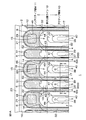
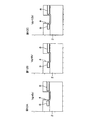
図1Aおよび図1Bは、本発明の一実施形態に係る半導体装置1の模式的な平面図である。明瞭化のために、図1Aではソースフィールドプレート8およびフローティングプレート9の領域をハッチングで示し、図1Bではソース電極5の領域をハッチングで示している。図1Aおよび図1Bは、ハッチングが付された領域が異なる点以外は同一である。
Hereinafter, embodiments of the present invention will be described in detail with reference to the accompanying drawings.
1A and 1B are schematic plan views of a
半導体装置1は、ベースとなるIII族窒化物半導体積層構造2上に、ドレイン電極3、ゲート電極4、ソース電極5およびプレート膜6を有している。たとえば、図1Aおよび図1Bに示すように、ドレイン電極3(D)、ゲート電極4(G)およびソース電極5(S)は、DGSGDの順に周期的に配置されている。これにより、ドレイン電極3およびソース電極5でゲート電極4を挟むことによって素子構造7が構成されている。プレート膜6は、ゲート−ソース間およびドレイン−ゲート間それぞれ配置されている。本発明の導電層の一例としてのソースフィールドプレート8がドレイン−ゲート間に配置され、本発明の第2導電層の一例としてのフローティングプレート9がゲート−ソース間に配置されている。
The
III族窒化物半導体積層構造2の表面には、当該素子構造7を含むアクティブ領域10と、アクティブ領域10外のノンアクティブ領域11とを定義できる。ノンアクティブ領域11は、図1Aおよび図1Bに示すようにアクティブ領域10に隣接しているだけでもよいし、アクティブ領域10を取り囲んでいてもよい。
ソース電極5は、ノンアクティブ領域11上の本発明の延長部の一例としてのベース部12と、当該ベース部12に一体的に接続された複数の電極部13とを含む。この実施形態のソース電極5は、複数の電極部13が互いに平行なストライプ状に延びる櫛歯状である。ベース部12は、ノンアクティブ領域11内に、電極部13用の接続端部14を有している。複数の電極部13は、当該接続端部14からアクティブ領域10へ向かって延びている。つまり、複数の電極部13は、アクティブ領域10およびノンアクティブ領域11の間に跨っている。
An
The
隣り合う電極部13の間のスペース15は、ドレイン電極3が配置された領域である。この実施形態では、各スペース15に直線状のドレイン電極3が配置されることによって、二つの櫛歯状のソース電極5およびドレイン電極3が、互いに係合している。なお、図示はしていないが、ドレイン電極3は、ソース電極5と同様に、ノンアクティブ領域11上のベース部と、当該ベース部に一体的に接続された複数の電極部(スペース15に配置される部分)とを含んでいてもよい。
A
ゲート電極4は、ノンアクティブ領域11上のベース部16と、当該ベース部16に一体的に接続された複数の電極部17とを含む。この実施形態のゲート電極4は、複数の電極部17が互いに平行なストライプ状に延びる櫛歯状である。ベース部16は、ノンアクティブ領域11内に、電極部17用の接続端部18を有している。接続端部18は、アクティブ領域10とノンアクティブ領域11との境界(素子分離ライン19)を基準に、ソース電極5の接続端部14よりも外側(相対的にアクティブ領域10から遠い側)に設けられている。複数の電極部17は、当該接続端部18からアクティブ領域10へ向かって延びている。つまり、複数の電極部17は、アクティブ領域10およびノンアクティブ領域11の間に跨っている。また、ゲート電極4のベース部16は、ソース電極5のベース部12よりも外側の引き出し部20を含む。たとえば、引き出し部20は、ゲート電極4に対するコンタクトを形成するための領域である。
The
ソースフィールドプレート8は、ノンアクティブ領域11上に本発明の延長部の一例としてのベース部21と、当該ベース部21に一体的に接続された複数の電極部54とを含む。この実施形態のソースフィールドプレート8は、ベース部21の両端部から一対の電極部54が延びるアーチ状である。ベース部21は、ノンアクティブ領域11内に、電極部54用の接続端部22を有している。接続端部22は、素子分離ライン19を基準に、ソース電極5の接続端部14とほぼ同じ位置に設けられている。一対の電極部54は、当該接続端部22からアクティブ領域10へ向かって延びている。つまり、一対の電極部54は、アクティブ領域10およびノンアクティブ領域11の間に跨っている。
The
ソース電極5のベース部12とソースフィールドプレート8のベース部21は、ノンアクティブ領域11内で部分的に重なっている。この重なり部分において、ソース電極5およびソースフィールドプレート8は、ソースコンタクト23を介して接続されている。たとえば、ソースコンタクト23は、図1Aおよび図1Bに示すように、スペース15に対向する位置(電極部13の延長部を避けた位置)に設けられている。
The
このようにソースコンタクト23をノンアクティブ領域11に設ければ、ソース電極5とソースフィールドプレート8とを電気的に接続するための構造として、ゲート電極4の上方を跨いでソース電極5およびソースフィールドプレート8のそれぞれに電気的に接続される導電構造をアクティブ領域10に設ける必要がない。このような導電構造がアクティブ領域10に設けられると半導体装置1の寄生容量を増加させる要因になり得るが、上記のようにノンアクティブ領域11でソース電極5とソースフィールドプレート8とを接続することによって、寄生容量の増加を抑制することができる。
If the
フローティングプレート9は、ノンアクティブ領域11上にベース部51と、当該ベース部51に一体的に接続された複数の電極部55とを含む。この実施形態のフローティングプレート9は、ベース部51の両端部から一対の電極部55が延びるアーチ状である。ベース部51は、ノンアクティブ領域11内に、電極部55用の接続端部52を有している。接続端部52は、素子分離ライン19を基準に、ソース電極5の接続端部14とほぼ同じ位置に設けられている。一対の電極部55は、当該接続端部52からアクティブ領域10へ向かって延びている。つまり、一対の電極部55は、アクティブ領域10およびノンアクティブ領域11の間に跨っている。
The floating
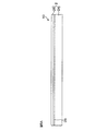
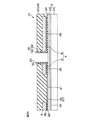
次に、図2および図3を主に参照して、半導体装置1の断面構造を説明する。
図2は、半導体装置1の断面図(図1Aおよび図1BのII−II線断面図)である。図3は、半導体装置1の要部拡大図(図2の破線IIIの内方領域)である。
III族窒化物半導体積層構造2は、図3に示すように、本発明の第1半導体層の一例としての電子走行層24と、電子走行層24上の本発明の第2半導体層の一例としての電子供給層25とを含む。電子走行層24および電子供給層25は、互いにAl組成の異なるIII族窒化物半導体からなっている。たとえば、電子走行層24は、GaN層からなっていてもよく、その厚さは、0.1μm〜3μmであってもよい。たとえば、電子供給層25は、AlN層からなっていてもよく、その厚さは、1nm〜7nmであってもよい。なお、電子走行層24および電子供給層25は、ヘテロ接合を形成して二次元電子ガスを発生させることができる組成であれば特に限定されず、それぞれ、AlxGa1−xN層(0≦x≦1)およびAlyGa1−yN層(0≦y≦1)からなっていてもよい。
Next, a cross-sectional structure of the
2 is a cross-sectional view of the semiconductor device 1 (a cross-sectional view taken along the line II-II in FIGS. 1A and 1B). FIG. 3 is an enlarged view of a main part of the semiconductor device 1 (inner region of broken line III in FIG. 2).
As shown in FIG. 3, the group III nitride
このように、電子走行層24と電子供給層25とは、互いにAl組成の異なる窒化物半導体からなっており、それらの間には格子不整合が生じている。そして、この格子不整合に起因する分極のために、電子走行層24と電子供給層25との界面に近い位置(たとえば界面から数Å程度の距離の位置)には、その分極に起因する二次元電子ガス26が広がっている。
Thus, the
電子供給層25には、その表面から電子走行層24に至るように、酸化膜27が選択的に形成されている。酸化膜27は、電子供給層25とほぼ等しい膜厚を有している。たとえば、酸化膜27は、熱酸化膜であり、電子走行層24との界面に損傷を与えることなく形成された酸化膜である。電子供給層25がAlN層である場合、酸化膜27は、AlON膜からなっていてもよい。
An
なお、III族窒化物半導体積層構造2は、シリコン基板等の基板上に、バッファ層を介して積層されていてもよい。
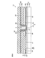
半導体装置1は、III族窒化物半導体積層構造2上に形成された、下地層28および絶縁層29をさらに含む。
下地層28は、ドレイン電極3およびソース電極5の形成領域を含むIII族窒化物半導体積層構造2の表面全体に形成されている。たとえば、下地層28は、SiN膜からなっていてもよく、その厚さは、5nm〜200nmであってもよい。
Group III nitride
The
絶縁層29は、下地層28を覆っており、第1層30および当該第1層30上の第2層31を含む。たとえば、第1層30および第2層31は、共にSiO2膜からなっていてもよい。また、絶縁層29は、1.5μm〜2μmの厚さを有していてもよい。個別には、第1層30が500nm〜1000nmの厚さを有し、第2層31が500nm〜1000nmの厚さを有していてもよい。
The insulating
第1層30および下地層28には、III族窒化物半導体積層構造2に達するゲート開口部32が形成されている。ゲート開口部32の底部には、酸化膜27が露出している。ゲート開口部32の底部および側部を覆うようにゲート絶縁膜33が形成されている。ゲート絶縁膜33は、ゲート開口部32内に加えて、第1層30と第2層31との間にも形成されている。たとえば、ゲート絶縁膜33は、構成元素としてSi、AlおよびHfからなる群から選択される少なくとも一種の材料膜からなっていてもよい。より具体的には、ゲート絶縁膜33は、SiN、SiO2、SiON、Al2O3、AlN、AlON、HfSiOおよびHfO2等からなる群から選択される少なくとも一種の材料膜からなっていてもよい。これらのうち、好ましくは、Al2O3膜が挙げられる。また、ゲート絶縁膜33は、10nm〜100nmの厚さを有していてもよい。
A
ゲート電極4は、ゲート開口部32に埋め込まれている。たとえば、ゲート電極4は、ゲート開口部32の開口端よりも上方に出っ張らないようにゲート開口部32に充填されていてもよい。代わりに、ゲート電極4は、図3に破線で示すように、ゲート開口部32の周縁でゲート絶縁膜33上に形成されたオーバーラップ部34を含んでいてもよい。たとえば、ゲート電極4は、Mo、Ni等の金属電極からなっていてもよいし、ドープトポリシリコン等の半導体電極からなっていてもよい。金属電極はポリシリコンに比べて埋め込み性に劣るので、金属電極を用いた場合に、特にオーバーラップ部34が形成され易い。
The
ソースフィールドプレート8およびフローティングプレート9は、ゲート開口部32の側部を部分的に形成するように、ゲート電極4の側方に配置されている。具体的には、ソースフィールドプレート8およびフローティングプレート9は、ゲート開口部32の側部の下側で露出するように、下地層28上に、絶縁膜36を介して形成されている。つまり、ゲート開口部32の側部は、下側がソースフィールドプレート8およびフローティングプレート9で形成され、上側が絶縁層29(第1層30)で形成されることによって、導電層/絶縁層の積層界面を有している。
The
そして、ソースフィールドプレート8およびフローティングプレート9に接するように、ゲート開口部32の側部に絶縁性のサイドウォール35が形成されている。つまり、サイドウォール35は、ゲート開口部32の側部とゲート絶縁膜33との間に配置されている。たとえば、サイドウォール35は、SiO2、SiNおよびSiONからなる群から選択される少なくとも一種の材料膜からなっていてもよい。これらのうち、好ましくは、SiO2膜が挙げられる。また、サイドウォール35は、10nm〜200nmの厚さを有していてもよい。
An insulating
ソースフィールドプレート8およびフローティングプレート9は、サイドウォール35およびゲート絶縁膜33によって、ゲート電極4から絶縁されている。たとえば、ゲート電極4とソースフィールドプレート8およびフローティングプレート9との距離LGFは、1μm以下であり、好ましくは、50nm〜200nmであってよい。距離LGFは、この実施形態ではゲート絶縁膜33およびサイドウォール35の総厚さで定義されるが、サイドウォール35を有しない構成では、距離LGF=ゲート絶縁膜33の厚さであってもよい。また、ソースフィールドプレート8の長さLFPは、たとえば、ゲート電極4とドレイン電極3との距離LGDと間に、LFP<1/3LGDを満たしている。たとえば、半導体装置1の耐圧が200V以下の場合、長さLFPは0.25μm〜1.5μmであってよく、距離LGDは1μm〜6μmであってよい。また、ソースフィールドプレート8およびフローティングプレート9は、Mo膜からなっていてもよく、その厚さは、10nm〜200nmであってもよい。
The
絶縁層29および下地層28には、III族窒化物半導体積層構造2に達する、ソースコンタクトホール37およびドレインコンタクトホール38が形成されている。ソースコンタクトホール37およびドレインコンタクトホール38は、ゲート開口部32から横方向に離れた位置に形成されている。ソースコンタクトホール37およびドレインコンタクトホール38には、それぞれ、ソース電極5およびドレイン電極3が埋め込まれている。ソース電極5およびドレイン電極3は、それぞれ、ソースコンタクトホール37およびドレインコンタクトホール38内でIII族窒化物半導体積層構造2に電気的に接続されている。
In the insulating
ソースコンタクトホール37およびドレインコンタクトホール38は、下地層28の部分で、絶縁層29の部分よりも相対的に大きなオーミックコンタクト開口39,40を有している(オーミックコンタクト開口39は図1A、図1Bおよび図3参照、オーミックコンタクト開口40は図1Aおよび図1B参照)。ソース電極5およびドレイン電極3は、それぞれ、オーミックコンタクト開口39,40にオーミック電極41,42を有し、絶縁層29内にパッド電極43,44を有している。図1Aおよび図1Bに示すように、オーミック電極41,42は、スペース15の奥行き方向における端部が互いに同じ位置に配置されているが、たとえば、ドレイン側のオーミック電極42の端部が選択的に後退していてもよい。パッド電極43,44は、オーミック電極41,42上に形成され、その頂部が絶縁層29の表面から露出している。たとえば、オーミック電極41,42およびパッド電極43,44は、Ti/Al膜からなっていてもよい。
The
なお、この実施形態では図3と異なる位置での切断面に現れる構成であるが、絶縁層29には、ソースフィールドプレート8に達するコンタクトホール46が形成されていてもよい。このコンタクトホール46には、図1に示したソースコンタクト23が埋め込まれ、ソースフィールドプレート8に接続されていてもよい。
この半導体装置1では、前述したように、電子走行層24上にAl組成の異なる電子供給層25が形成されてヘテロ接合が形成されている。これにより、電子走行層24と電子供給層25との界面付近の電子走行層24内に二次元電子ガス26が形成され、この二次元電子ガス26をチャネルとして利用したHEMTが形成されている。ゲート電極4は、酸化膜27およびゲート絶縁膜33の積層膜を挟んで電子走行層24に対向しており、ゲート電極4の直下には、電子供給層25は存在しない。したがって、ゲート電極4の直下では、電子供給層25と電子走行層24との格子不整合による分極に起因する二次元電子ガス26が形成されない。よって、ゲート電極4にバイアスを印加していないとき(ゼロバイアス時)には、二次元電子ガス26によるチャネルはゲート電極4の直下で遮断されている。こうして、ノーマリオフ型のHEMTが実現されている。ゲート電極4に適切なオン電圧(たとえば5V)を印加すると、ゲート電極4の直下の電子走行層24内にチャネルが誘起され、ゲート電極4の両側の二次元電子ガス26が接続される。これにより、ソース−ドレイン間が導通する。
In this embodiment, the structure appears on a cut surface at a position different from that in FIG. 3, but a
In the
使用に際しては、たとえば、ソース電極5とドレイン電極3との間に、ドレイン電極3側が正となる所定の電圧(たとえば200V〜400V)が印加される。その状態で、ゲート電極4に対して、ソース電極5を基準電位(0V)として、オフ電圧(0V)またはオン電圧(5V)が印加される。
酸化膜27と電子走行層24との界面は、電子供給層25と電子走行層24との界面に連続していて、ゲート電極4の直下における電子走行層24の界面の状態は、電子供給層25と電子走行層24との界面の状態と同等である。そのため、ゲート電極4の直下の電子走行層24における電子移動度は高い状態に保持されている。こうして、この実施形態は、ノーマリオフ型のHEMT構造を有する窒化物半導体装置を提供する。
In use, for example, a predetermined voltage (for example, 200 V to 400 V) that is positive on the
The interface between the
次に、図4および図5A〜図5Oを参照して、半導体装置1の製造方法を説明する。
図4は、半導体装置1の製造方法を説明するためのフロー図である。図5A〜図5Oは、半導体装置1の製造工程を工程順に示す図である。
半導体装置1を製造するには、たとえば、基板(図示せず)上に、バッファ層(図示せず)および電子走行層24が順にエピタキシャル成長させられ、図5Aに示すように、さらに電子走行層24上に電子供給層25がエピタキシャル成長させられる。これにより、III族窒化物半導体積層構造2が形成される(ステップS1)。
Next, a method for manufacturing the
FIG. 4 is a flowchart for explaining the method for manufacturing the
In order to manufacture the
次に、図5Bに示すように、電子供給層25上の全面を覆うように、たとえば、CVD法(化学的気相成長法)によって、下地層28が形成される(ステップS2)。
次に、図5Cに示すように、たとえば、ドライエッチングによって、下地層28が選択的に除去される(ステップS3)。これにより、ソースコンタクトホール37のオーミックコンタクト開口39およびドレインコンタクトホール38のオーミックコンタクト開口40が同時に形成される(図5Cおよびそれ以降では、ドレインコンタクトホール38の図示およびその説明を省略)。
Next, as shown in FIG. 5B, the
Next, as shown in FIG. 5C, for example, the
次に、図5Dに示すように、オーミックコンタクト開口39内に、オーミック電極41が形成される(ステップS4)。図5Cで示したように、オーミックコンタクト開口39の形成に当たって、後の工程で形成される絶縁層29に比べて薄い膜である下地層28のエッチングだけで済む。そのため、絶縁層29をエッチングして開口を形成する場合に比べて、III族窒化物半導体積層構造2の表面に与えるダメージを低減することができる。その結果、ダメージの少ないIII族窒化物半導体積層構造2の表面にオーミック電極41(ソース電極5)を接続できるので、良好なオーミックコンタクトを得ることができる。
Next, as shown in FIG. 5D, the
次に、図5Eに示すように、電子供給層25上の全面を覆うように、たとえば、CVD法(化学的気相成長法)によって、絶縁膜36が形成され、さらに、スパッタ法、蒸着法等によって、絶縁膜36上に本発明の導電層の一例としてのプレート膜45が形成される(ステップS5)。
次に、図5Fに示すように、たとえば、ドライエッチングによって、プレート膜45が選択的に除去される(ステップS6)。これにより、ソース電極5の形成領域とドレイン電極3の形成領域の各間に、プレート膜6が形成される。隣り合うプレート膜6の間の距離は、少なくとも、後の工程で形成されるソースコンタクトホール37の開口径よりも大きく、好ましくは、図5Fに示すように、オーミックコンタクト開口39の開口径よりも大きくされる。こうすることにより、ソースコンタクトホール37の形成時に横方向に位置ずれしても、ソース電極5とプレート膜6との接触を防止することができる。つまり、これは、ソース電極5が、ソースコンタクト23以外の部分でプレート膜6に接続されることを防止する。
Next, as shown in FIG. 5E, an insulating
Next, as shown in FIG. 5F, the
次に、図5Gに示すように、電子供給層25上の全面を覆うように、たとえば、CVD法(化学的気相成長法)によって、絶縁層29の第1層30が形成される(ステップS7)。これにより、プレート膜6は、第1層30に埋め込まれる。
次に、図5Hに示すように、プレート膜6に対向する領域を含むエッチング領域から第1層30およびプレート膜6をエッチングすることによって、ゲート開口部32が形成される(ステップS8)。これにより、プレート膜6は、ゲート開口部32に対して自己整合的に、ドレイン側のソースフィールドプレート8とソース側のフローティングプレート9とに分離される。したがって、ソースフィールドプレート8およびフローティングプレート9は、この段階では、ゲート開口部32の側部に露出することになる。
Next, as shown in FIG. 5G, the
Next, as shown in FIG. 5H, the
次に、図5Iに示すように、電子供給層25上の全面を覆うように、たとえば、CVD法(化学的気相成長法)によって、絶縁膜47が形成される(ステップS9)。絶縁膜47を形成する工程は、絶縁層29に接する下層膜48を形成する工程と、絶縁膜47の最表面を形成する上層膜49を形成する工程とを含むことによって、絶縁膜の積層構造を形成する工程を含んでいてもよい。当該積層構造は、二層構造からなっていてもよいし、三層以上の構造からなっていてもよい。たとえば、下層膜48は、SiO2膜からなっていてもよく、上層膜49は、Al2O3膜からなっていてもよい。絶縁層29および下層膜48が共にSiO2膜である場合、絶縁層29に対する絶縁膜47(下層膜48)の密着性を高めることができる。そのため、後の工程において、サイドウォール35の膜剥がれを防止することができる。
Next, as shown in FIG. 5I, an insulating
次に、図5Jに示すように、たとえば、エッチバックによって、絶縁膜47の絶縁層29上の部分が選択的に除去され、ゲート開口部32の側部上にサイドウォール35が形成される(ステップS10)。上層膜49としてAl2O3膜を採用していると、エッチバック後に、エッチングされ難いAl2O3膜の一部がゲート開口部32から上方への突出部50として残ることがある。
Next, as shown in FIG. 5J, the portion of the insulating
次に、図5Kに示すように、たとえば、ドライエッチングによって、ゲート開口部32の底部における下地層28が選択的に除去される(ステップS11)。これにより、ゲート開口部32の底部にIII族窒化物半導体積層構造2の電子供給層25が露出する。下地層28がSiN膜であり、上層膜49がAl2O3膜である場合、下地層28用のエッチャント(たとえば、CF4ガス等)に対して上層膜49のエッチング選択比を小さくすることができる。したがって、下地層28をエッチングする際に、下層膜48を上層膜49で保護できるので、サイドウォール35(下層膜48)が下地層28と一緒にエッチングされて薄くなることを抑制することができる。そのため、下地層28のエッチング後においても、設計値に近い厚さを有するサイドウォール35を維持することができる。
Next, as shown in FIG. 5K, the
次に、図5Lに示すように、たとえば、ドライエッチングによって、サイドウォール35の表面部が選択的に除去される。この実施形態では、最表面を形成する上層膜49が選択的に除去されることによって、下層膜48がサイドウォール35として残ることとなる。上層膜49がAl2O3膜である場合、たとえば、BCl3ガスがエッチャントとして使用されてもよい。その後、電子供給層25のゲート開口部32に露出した部分が選択的に酸化されることによって、電子供給層25の一部が酸化膜27となる。
Next, as shown in FIG. 5L, for example, the surface portion of the
次に、図5Mに示すように、電子供給層25上の全面を覆うように、たとえば、CVD法(化学的気相成長法)によって、ゲート絶縁膜33が形成され、さらにゲート絶縁膜33の内側にゲート電極4が埋め込まれる(ステップS13)。ゲート電極4の形成後、電子供給層25上の全面を覆うように、たとえば、CVD法(化学的気相成長法)によって、第2層31が形成される。
Next, as illustrated in FIG. 5M, a
次に、図5Nに示すように、オーミック電極41およびソースフィールドプレート8に対向する領域を含むエッチング領域から第2層31、ゲート絶縁膜33および第1層30が、たとえば、ドライエッチングによって、選択的に除去される。これにより、ソースコンタクトホール37、ドレインコンタクトホール38(図1A、図1Bおよび図2参照)およびコンタクトホール46が同時に形成される(ステップS14)。
Next, as shown in FIG. 5N, the
次に、図5Oに示すように、電子供給層25上の全面を覆うように、たとえば、スパッタ法、蒸着法等によって、絶縁層29上に電極膜が形成され、この電極膜をパターニングすることによって、ソース電極5(パッド電極43)、ドレイン電極3(パッド電極44)およびソースコンタクト23が形成される(ステップS15)。以上の工程を経て、図1A〜図3に示す半導体装置1が得られる。
Next, as shown in FIG. 5O, an electrode film is formed on the insulating
以上の方法によれば、図5Hに示すように、ソースフィールドプレート8が、ゲート開口部32の形成の際にセルフアライメントプロセスで形成される。これにより、ソースフィールドプレート8がゲート開口部32の側部に露出するので、ソースフィールドプレート8のゲート電極4に近い側の端部位置を、ゲート開口部32の側部に固定することができる。そのため、図3に示すように、ゲート電極4とソースフィールドプレート8との距離LGFを、ゲート絶縁膜33およびサイドウォール35によって簡単に制御することができる。その結果、半導体装置1内の最大電界強度を、意図した値に設計することができる。したがって、ゲート電極4およびソースフィールドプレート8の各端部への電界集中を緩和できる構造を実現することができる。
According to the above method, as shown in FIG. 5H, the
この効果は、たとえば、図6〜図8を参照して証明することができる。図6は、シミュレーションのモデル図である。
このシミュレーションモデルでは、図3の主な構成に関して次の条件を設定した。
・III族窒化物半導体積層構造2:GaN(1.0μm,1×1016cm−3)/AlGaN
・下地層28:SiN,100nm
・絶縁膜36:Al2O3,40nm
・ソースフィールドプレート(SFP)8:長さLFP
・絶縁層29:SiO2,300nm
・ゲート絶縁膜33:Al2O3,40nm
・サイドウォール35:SiO2,厚さLSW
このような条件下において、ソースフィールドプレート8の長さLFPおよびサイドウォール35の厚さLSWを変化させたときに(LGD=6.0μm、VDS=200V)、電界強度分布がどのように変化するのかをシミュレーションした。結果を、図7および図8に示す。
This effect can be proved, for example, with reference to FIGS. FIG. 6 is a model diagram of simulation.
In this simulation model, the following conditions were set for the main configuration of FIG.
Group III nitride semiconductor multilayer structure 2: GaN (1.0 μm, 1 × 10 16 cm −3 ) / AlGaN
・ Underlayer 28: SiN, 100 nm
Insulating film 36: Al 2 O 3 , 40 nm
Source field plate (SFP) 8: Length L FP
Insulating layer 29: SiO 2 , 300 nm
Gate insulating film 33: Al 2 O 3 , 40 nm
-Sidewall 35: SiO 2 , thickness L SW
Under such conditions, when the length L FP of the
図7は、シミュレーションモデルにおけるLFPと最大電界強度との関係を示すグラフである。図7では、LFP=0μm(つまり、ソースフィールドプレート8なし)のときを1として、測定値を規格化している。図7によれば、ソースフィールドプレート8の設置によって、最大電界強度を緩和できていることが分かる。そして、この電界緩和効果は、LFP>1μm(=1/6LGD)で飽和することから、長さLFPの増加に伴うドレイン−ソース間容量Cdsの増加を考慮して、長さLFPは、少なくとも距離LGDの1/3未満程度であることが好ましい。
FIG. 7 is a graph showing the relationship between LFP and maximum electric field strength in the simulation model. In FIG. 7, the measurement value is normalized by assuming 1 when L FP = 0 μm (that is, no source field plate 8). As can be seen from FIG. 7, the maximum electric field strength can be relaxed by the installation of the
一方、図8は、シミュレーションモデルにおけるLSWと最大電界強度との関係を示すグラフである。図8では、LSW=50nmのときを1として、測定値を規格化している。図8によれば、最大電界強度は、サイドウォール35の厚さLSWに依存しないことが分かる。言い換えれば、図8は、図3に示したゲート電極4とソースフィールドプレート8との距離LGFは、小さくても大きくても、最大電界強度に与える影響が低いことを示している。したがって、ゲート絶縁膜33およびサイドウォール35の厚さを調節して、ソースフィールドプレート8をゲート電極4の比較的近く(たとえば、1μm以下)に配置することによって、ソースフィールドプレート8の端部への電界集中を良好に緩和することができる。
On the other hand, FIG. 8 is a graph showing the relationship between LSW and maximum electric field strength in the simulation model. In FIG. 8, the measurement value is normalized by setting 1 when L SW = 50 nm. As can be seen from FIG. 8, the maximum electric field strength does not depend on the thickness L SW of the
さらに、図6のモデルを用いて、III族窒化物半導体積層構造2におけるチャネルの広がりについても検証した。図9A〜図9Cおよび図10A〜図10Cは、シミュレーションモデル(SFPなし)におけるチャネルの広がりを示す図である。図11A〜図11Cおよび図12A〜図12Cは、シミュレーションモデル(SFPあり)におけるチャネルの広がりを示す図である。
Furthermore, using the model of FIG. 6, the channel spread in the group III nitride
図11A〜図11Cおよび図12A〜図12Cから、半導体装置1のようにMIS構造を用いたノーマリオフ型のGaN−HEMTでは、ソースフィールドプレート8が存在すると、ゲート電圧によって発生するキャリアがソースフィールドプレート8の直下に広がらない結果が得られている。このような場合に、たとえば、ソースフィールドプレート8の直下に酸化膜領域が形成されるなどして二次元電子ガス26のキャリアが存在していないと、ソースフィールドプレート8の直下の酸化膜領域でポテンシャルが高くなることがある。そのため、ゲート電極4に比較的高いバイアスを印加しなければポテンシャルが下がらず、ソース−ドレイン間に電流が流れないおそれがある。この点、この実施形態では、図5Hに示すように、ソースフィールドプレート8が、ゲート開口部32の形成の際にセルフアライメントプロセスで形成される。そのため、ソースフィールドプレート8の直下に酸化膜27が形成されることがない。したがって、ゲート電極4とソースフィールドプレート8との距離LGFを最大限に小さくすることによって、比較的低いゲート電圧でチャネルを形成できるので、デバイスのオン特性を最大限に引き出すことができる。しかも、このような構造を、ゲート絶縁膜33およびサイドウォール35の厚さを調節という簡単な手法で実現することができる。また、この実施形態によれば、サイドウォール35が備えられているため、ゲート電極4とソースフィールドプレート8との距離LGFを、主にサイドウォール35の厚さによって制御することできる。そのため、ゲート絶縁膜33の厚さを、主に、意図したゲートしきい値電圧に合わせて設計することができる。
From FIG. 11A to FIG. 11C and FIG. 12A to FIG. 12C, in the normally-off type GaN-HEMT using the MIS structure as in the
そして、半導体装置1では、ソース電極5に電気的に接続されたソースフィールドプレート8が、ゲート−ドレイン間に配置されている。これにより、ゲート電極4から一体的に絶縁層29上を横方向に延びるゲートフィールドプレートを設けなくて済むので、ゲート−ドレイン間容量Cgdを低減することができる。その結果、半導体装置1の寄生容量を低減することができるので、窒化物半導体系デバイスの特徴である高速スイッチング動作、高周波動作等を良好に発揮することができる。この効果は、たとえば、図13を参照して証明することができる。
In the
図13は、寄生容量の評価結果を示す図である。図13において、実線が、ソースフィールドプレート(SFP)8を備えている半導体装置1の各寄生容量の変化を示しており、破線が、ソースフィールドプレート8に代えてゲートフィールドプレート(GFP)を備えている半導体装置の各寄生容量の変化を示している。
図13によれば、SFP構造では、ソース電位のソースフィールドプレート8とドレイン電位の二次元電子ガス26とが対向することになるため(図3参照)、低電圧領域でCoss(=Cds+Cgd)が大きくなる傾向があるが、Ciss(=Cgs+Cgd)およびCrss(=Cgd)を含めた寄生容量全体で判断したときには、GFP構造よりも容量を低減できていることが分かる。
FIG. 13 is a diagram illustrating the evaluation result of the parasitic capacitance. In FIG. 13, solid lines indicate changes in the parasitic capacitances of the
According to FIG. 13, in the SFP structure, since the
以上、本発明の実施形態について説明したが、本発明は、さらに他の形態で実施することも可能である。
たとえば、図14に示す半導体装置61は、ノーマリオフ型のHEMTを実現する構造として、酸化膜27に代えて、リセス53を有している。リセス53は、たとえば、ゲート開口部32の底部のみを選択的にエッチングすることによって、電子供給層25を貫通し、電子走行層24の表層部に至るように形成されていてもよい。リセス53によって、ゲート電極4の直下における電子走行層24と電子供給層25とのヘテロ接合の形成が防止される。これにより、ゲートバイアスを印加しないとき(ゼロバイアス時)には当該直下領域に二次元電子ガス26が形成されないので、ノーマリオフ型のHEMTを実現することができる。
As mentioned above, although embodiment of this invention was described, this invention can also be implemented with another form.
For example, the
また、半導体装置1は、サイドウォール35を備えていなくてもよい。この場合、ゲート絶縁膜33のみの厚さに基づいて、ゲート電極4とソースフィールドプレート8との距離LGFを制御することができる。
また、半導体装置1は、ソース−ゲート間のフローティングプレート9を備えていなくてもよい。つまり、ソース−ゲート間およびゲート−ドレイン間のうち、後者のみに選択的にフィールドプレート(ソースフィールドプレート8)が設けられていてもよい。このような構成は、たとえば、図5Hに示すエッチング時に、エッチング領域を、プレート膜6の端部の内外に跨る領域として設定すればよい。
Further, the
Further, the
その他、特許請求の範囲に記載された事項の範囲で種々の設計変更を施すことが可能である。 In addition, various design changes can be made within the scope of matters described in the claims.
1 半導体装置
2 III族窒化物半導体積層構造
3 ドレイン電極
4 ゲート電極
5 ソース電極
6 プレート膜
7 素子構造
8 ソースフィールドプレート
9 フローティングプレート
10 アクティブ領域
11 ノンアクティブ領域
12 (ソース電極)ベース部
13 (ソース電極)電極部
21 (ソースフィールドプレート)ベース部
23 ソースコンタクト
24 電子走行層
25 電子供給層
26 二次元電子ガス
27 酸化膜
28 下地層
29 絶縁層
30 第1層
31 第2層
32 ゲート開口部
33 ゲート絶縁膜
34 オーバーラップ部
35 サイドウォール
41 オーミック電極
42 オーミック電極
43 パッド電極
44 パッド電極
45 プレート膜
47 絶縁膜
49 上層膜
50 突出部
53 リセス
54 (ソースフィールドプレート)電極部
61 半導体装置
DESCRIPTION OF
Claims (17)
前記III族窒化物半導体積層構造に達するゲート開口部を有する、前記III族窒化物半導体積層構造上の絶縁層と、
前記ゲート開口部の底部および側部を覆うゲート絶縁膜と、
前記ゲート開口部内で前記ゲート絶縁膜上に形成されたゲート電極と、
前記ゲート電極を挟むように前記ゲート電極から離れて配置され、それぞれ前記III族窒化物半導体積層構造に電気的に接続されたソース電極およびドレイン電極と、
前記ゲート電極と前記ドレイン電極との間で前記絶縁層に埋め込まれ、前記ゲート絶縁膜によって前記ゲート電極から絶縁された導電層であって、前記ソース電極に電気的に接続された導電層と、
前記ゲート絶縁膜と前記ゲート開口部の側部との間に配置された絶縁性のサイドウォールとを含む、半導体装置。 A group III nitride semiconductor multilayer structure including a heterojunction;
An insulating layer on the group III nitride semiconductor multilayer structure having a gate opening reaching the group III nitride semiconductor multilayer structure;
A gate insulating film covering the bottom and sides of the gate opening;
A gate electrode formed on the gate insulating film in the gate opening;
A source electrode and a drain electrode that are arranged apart from the gate electrode so as to sandwich the gate electrode, and are electrically connected to the group III nitride semiconductor multilayer structure,
A conductive layer embedded in the insulating layer between the gate electrode and the drain electrode and insulated from the gate electrode by the gate insulating film, the conductive layer electrically connected to the source electrode ;
A semiconductor device comprising: an insulating sidewall disposed between the gate insulating film and a side portion of the gate opening .
前記III族窒化物半導体積層構造に達するゲート開口部を有する、前記III族窒化物半導体積層構造上の絶縁層と、 An insulating layer on the group III nitride semiconductor multilayer structure having a gate opening reaching the group III nitride semiconductor multilayer structure;
前記ゲート開口部の底部および側部を覆うゲート絶縁膜と、 A gate insulating film covering the bottom and sides of the gate opening;
前記ゲート開口部内で前記ゲート絶縁膜上に形成されたゲート電極と、 A gate electrode formed on the gate insulating film in the gate opening;
前記ゲート電極を挟むように前記ゲート電極から離れて配置され、それぞれ前記III族窒化物半導体積層構造に電気的に接続されたソース電極およびドレイン電極と、 A source electrode and a drain electrode that are arranged apart from the gate electrode so as to sandwich the gate electrode, and are electrically connected to the group III nitride semiconductor multilayer structure,
前記ゲート電極と前記ドレイン電極との間で前記絶縁層に埋め込まれ、前記ゲート絶縁膜によって前記ゲート電極から絶縁された導電層であって、前記ソース電極に電気的に接続された導電層と、 A conductive layer embedded in the insulating layer between the gate electrode and the drain electrode and insulated from the gate electrode by the gate insulating film, the conductive layer electrically connected to the source electrode;
前記ゲート電極と前記ソース電極との間で前記絶縁層に埋め込まれ、前記ゲート絶縁膜によって前記ゲート電極から絶縁され、かつ、前記ソース電極からも絶縁された第2導電層とを含む、半導体装置。 A semiconductor device comprising: a second conductive layer embedded in the insulating layer between the gate electrode and the source electrode, insulated from the gate electrode by the gate insulating film, and also insulated from the source electrode .
前記ソース電極および前記導電層は、それぞれ、前記ノンアクティブ領域への延長部を含み、
前記ソース電極の延長部と前記導電層の延長部とが互いに接続されている、請求項1〜8のいずれか一項に記載の半導体装置。 The group III nitride semiconductor multilayer structure includes an active region including an element structure configured by sandwiching the gate electrode between the source electrode and the drain electrode, and a non-active region outside the active region,
The source electrode and the conductive layer each include an extension to the non-active region;
The semiconductor device according to claim 1, wherein the extension portion of the source electrode and the extension portion of the conductive layer are connected to each other.
前記第2半導体層は、前記ゲート開口部の底部に選択的に、当該第2半導体層の酸化によって形成された酸化膜を含む、請求項1〜9のいずれか一項に記載の半導体装置。 The group III nitride semiconductor multilayer structure includes a first semiconductor layer forming the heterojunction and a second semiconductor layer on the first semiconductor layer,
10. The semiconductor device according to claim 1, wherein the second semiconductor layer includes an oxide film formed selectively by oxidation of the second semiconductor layer at a bottom of the gate opening.
前記第2半導体層が、前記ゲート開口部の底部のみ選択的にエッチングされている、請求項1〜9のいずれか一項に記載の半導体装置。 The group III nitride semiconductor multilayer structure includes a first semiconductor layer forming the heterojunction and a second semiconductor layer on the first semiconductor layer,
The semiconductor device according to claim 1, wherein the second semiconductor layer is selectively etched only at the bottom of the gate opening.
前記ソース電極および/または前記ドレイン電極は、前記下地層内のオーミック電極と、前記オーミック電極上に形成された前記絶縁層内のパッド電極とを含む、請求項1〜11のいずれか一項に記載の半導体装置。 A base layer disposed between the conductive layer and the group III nitride semiconductor multilayer structure and extending to a formation region of the source electrode and the drain electrode;
The said source electrode and / or the said drain electrode are any one of Claims 1-11 containing the ohmic electrode in the said base layer, and the pad electrode in the said insulating layer formed on the said ohmic electrode. The semiconductor device described.
前記III族窒化物半導体積層構造に達するゲート開口部を有する、前記III族窒化物半導体積層構造上の絶縁層と、
前記ゲート開口部の底部および側部を覆うゲート絶縁膜と、
前記ゲート開口部内で前記ゲート絶縁膜上に形成されたゲート電極と、
前記ゲート電極を挟むように前記ゲート電極から離れて配置され、それぞれ前記III族窒化物半導体積層構造に電気的に接続されたソース電極およびドレイン電極と、
前記ゲート電極と前記ドレイン電極との間で前記ゲート開口部の側部を部分的に形成するように前記絶縁層に埋め込まれ、前記ゲート絶縁膜によって前記ゲート電極から絶縁されたソースフィールドプレートであって、前記ソース電極に電気的に接続されたソースフィールドプレートと、
前記ソースフィールドプレートに接するように前記ゲート開口部の側部に形成された絶縁性のサイドウォールとを含み、
前記ゲート絶縁膜は、前記サイドウォールを覆うように形成されている、半導体装置。 A group III nitride semiconductor multilayer structure including a heterojunction;
An insulating layer on the group III nitride semiconductor multilayer structure having a gate opening reaching the group III nitride semiconductor multilayer structure;
A gate insulating film covering the bottom and sides of the gate opening;
A gate electrode formed on the gate insulating film in the gate opening;
A source electrode and a drain electrode that are arranged apart from the gate electrode so as to sandwich the gate electrode, and are electrically connected to the group III nitride semiconductor multilayer structure,
A source field plate embedded in the insulating layer so as to partially form a side portion of the gate opening between the gate electrode and the drain electrode and insulated from the gate electrode by the gate insulating film. A source field plate electrically connected to the source electrode ;
An insulating sidewall formed on a side of the gate opening so as to be in contact with the source field plate,
The semiconductor device, wherein the gate insulating film is formed so as to cover the sidewall .
前記導電層を覆うように絶縁層を形成する工程と、
前記導電層の少なくとも一部に対向する領域を含むエッチング領域から前記絶縁層および前記導電層をエッチングすることによって、ゲート開口部を形成すると共に、当該ゲート開口部の側部に前記導電層を露出させる工程と、
前記ゲート開口部の底部および側部を覆うようにゲート絶縁膜を形成する工程と、
前記ゲート開口部内の前記ゲート絶縁膜上にゲート電極を形成する工程と、
前記ゲート電極との間に前記導電層を挟むように、前記III族窒化物半導体積層構造上にドレイン電極を形成する工程と、
前記ゲート電極を挟んで前記ドレイン電極の向かい側にソース電極を形成する工程とを含む、半導体装置の製造方法。 Forming a conductive layer on the group III nitride semiconductor multilayer structure including a heterojunction;
Forming an insulating layer so as to cover the conductive layer;
A gate opening is formed by etching the insulating layer and the conductive layer from an etching region including a region facing at least a part of the conductive layer, and the conductive layer is exposed at a side of the gate opening. A process of
Forming a gate insulating film so as to cover the bottom and sides of the gate opening;
Forming a gate electrode on the gate insulating film in the gate opening;
Forming a drain electrode on the group III nitride semiconductor multilayer structure so as to sandwich the conductive layer with the gate electrode;
Forming a source electrode on the opposite side of the drain electrode across the gate electrode.
前記ゲート開口部の底部および前記絶縁層の表面上の前記絶縁膜を選択的にエッチングすることによって、前記ゲート開口部の側部にサイドウォールを形成する工程とをさらに含む、請求項15に記載の半導体装置の製造方法。 Prior to the formation of the gate insulating film, forming an insulating film so as to cover the bottom and sides of the gate opening and the surface of the insulating layer;
The method of claim 15 , further comprising: forming a sidewall on the side of the gate opening by selectively etching the insulating film on the bottom of the gate opening and the surface of the insulating layer. Semiconductor device manufacturing method.
前記サイドウォールを形成する工程は、前記下地層よりも小さいエッチング選択比を有する絶縁材料を少なくとも最表面に有するサイドウォールを形成する工程を含み、
前記サイドウォールの形成後、前記ゲート開口部の底部の前記下地層を選択的にエッチングすることによって、前記ゲート開口部の底部を前記III族窒化物半導体積層構造に到達させる工程をさらに含む、請求項16に記載の半導体装置の製造方法。 Forming a base layer on the group III nitride semiconductor multilayer structure for insulating the conductive layer from the group III nitride semiconductor multilayer structure prior to forming the conductive layer;
The step of forming the sidewall includes a step of forming a sidewall having at least an insulating material having an etching selectivity smaller than that of the base layer on the outermost surface,
The method further comprises the step of, after forming the sidewall, selectively etching the base layer at the bottom of the gate opening to reach the bottom of the gate opening to the group III nitride semiconductor multilayer structure. Item 17. A method for manufacturing a semiconductor device according to Item 16 .
Priority Applications (2)
| Application Number | Priority Date | Filing Date | Title |
|---|---|---|---|
| JP2015010461A JP6496149B2 (en) | 2015-01-22 | 2015-01-22 | Semiconductor device and manufacturing method of semiconductor device |
| US15/003,772 US9704982B2 (en) | 2015-01-22 | 2016-01-21 | Semiconductor device with high electron mobility transistor (HEMT) having source field plate |
Applications Claiming Priority (1)
| Application Number | Priority Date | Filing Date | Title |
|---|---|---|---|
| JP2015010461A JP6496149B2 (en) | 2015-01-22 | 2015-01-22 | Semiconductor device and manufacturing method of semiconductor device |
Related Child Applications (1)
| Application Number | Title | Priority Date | Filing Date |
|---|---|---|---|
| JP2019042913A Division JP6689424B2 (en) | 2019-03-08 | 2019-03-08 | Semiconductor device |
Publications (2)
| Publication Number | Publication Date |
|---|---|
| JP2016134599A JP2016134599A (en) | 2016-07-25 |
| JP6496149B2 true JP6496149B2 (en) | 2019-04-03 |
Family
ID=56434193
Family Applications (1)
| Application Number | Title | Priority Date | Filing Date |
|---|---|---|---|
| JP2015010461A Active JP6496149B2 (en) | 2015-01-22 | 2015-01-22 | Semiconductor device and manufacturing method of semiconductor device |
Country Status (2)
| Country | Link |
|---|---|
| US (1) | US9704982B2 (en) |
| JP (1) | JP6496149B2 (en) |
Families Citing this family (8)
| Publication number | Priority date | Publication date | Assignee | Title |
|---|---|---|---|---|
| JP2019046991A (en) * | 2017-09-04 | 2019-03-22 | ルネサスエレクトロニクス株式会社 | Semiconductor device and manufacturing method of the same |
| JP6874928B2 (en) * | 2017-10-24 | 2021-05-19 | 住友電工デバイス・イノベーション株式会社 | Semiconductor device |
| JP7161915B2 (en) * | 2017-11-02 | 2022-10-27 | ローム株式会社 | semiconductor equipment |
| US10700188B2 (en) * | 2017-11-02 | 2020-06-30 | Rohm Co., Ltd. | Group III nitride semiconductor device with first and second conductive layers |
| JP7208167B2 (en) * | 2018-01-19 | 2023-01-18 | ローム株式会社 | Semiconductor device and its manufacturing method |
| CN109755301B (en) * | 2019-01-15 | 2024-05-31 | 中山大学 | GAN MISFET device with high-quality gate interface and preparation method thereof |
| US11075271B2 (en) * | 2019-10-14 | 2021-07-27 | Cree, Inc. | Stepped field plates with proximity to conduction channel and related fabrication methods |
| JP2021089934A (en) * | 2019-12-03 | 2021-06-10 | 株式会社東芝 | Semiconductor device |
Family Cites Families (14)
| Publication number | Priority date | Publication date | Assignee | Title |
|---|---|---|---|---|
| JPH07107906B2 (en) * | 1987-10-30 | 1995-11-15 | 株式会社東芝 | Method for manufacturing semiconductor device |
| JP2004311869A (en) * | 2003-04-10 | 2004-11-04 | Mitsubishi Electric Corp | Nitride semiconductor type field effect transistor and its manufacturing method |
| US7550783B2 (en) | 2004-05-11 | 2009-06-23 | Cree, Inc. | Wide bandgap HEMTs with source connected field plates |
| US7229903B2 (en) * | 2004-08-25 | 2007-06-12 | Freescale Semiconductor, Inc. | Recessed semiconductor device |
| JP2006086398A (en) * | 2004-09-17 | 2006-03-30 | Matsushita Electric Ind Co Ltd | Semiconductor device and its manufacturing method |
| JP2007335677A (en) * | 2006-06-15 | 2007-12-27 | Furukawa Electric Co Ltd:The | Normally-off field-effect transistor using group iii nitride semiconductor and its manufacturing method |
| US8283699B2 (en) * | 2006-11-13 | 2012-10-09 | Cree, Inc. | GaN based HEMTs with buried field plates |
| US7692263B2 (en) | 2006-11-21 | 2010-04-06 | Cree, Inc. | High voltage GaN transistors |
| US8309987B2 (en) * | 2008-07-15 | 2012-11-13 | Imec | Enhancement mode semiconductor device |
| US8860120B2 (en) * | 2010-09-22 | 2014-10-14 | Nxp, B.V. | Field modulating plate and circuit |
| JP2013168433A (en) * | 2012-02-14 | 2013-08-29 | Toshiba Corp | Nitride semiconductor device and method of manufacturing nitride semiconductor device |
| JP6085442B2 (en) * | 2012-09-28 | 2017-02-22 | トランスフォーム・ジャパン株式会社 | Compound semiconductor device and manufacturing method thereof |
| JP2014183125A (en) * | 2013-03-18 | 2014-09-29 | Fujitsu Ltd | Semiconductor device |
| JP6220161B2 (en) * | 2013-06-03 | 2017-10-25 | ルネサスエレクトロニクス株式会社 | Manufacturing method of semiconductor device |
-
2015
- 2015-01-22 JP JP2015010461A patent/JP6496149B2/en active Active
-
2016
- 2016-01-21 US US15/003,772 patent/US9704982B2/en active Active
Also Published As
| Publication number | Publication date |
|---|---|
| US20160218203A1 (en) | 2016-07-28 |
| US9704982B2 (en) | 2017-07-11 |
| JP2016134599A (en) | 2016-07-25 |
Similar Documents
| Publication | Publication Date | Title |
|---|---|---|
| JP6496149B2 (en) | Semiconductor device and manufacturing method of semiconductor device | |
| JP6090764B2 (en) | Nitride semiconductor device and manufacturing method thereof | |
| JP7539447B2 (en) | Semiconductor Device | |
| JP5487615B2 (en) | Field effect semiconductor device and manufacturing method thereof | |
| JP5776217B2 (en) | Compound semiconductor device | |
| JP4737471B2 (en) | Semiconductor device and manufacturing method thereof | |
| WO2014057906A1 (en) | Nitride semiconductor device and fabrication method therefor | |
| JP7547518B2 (en) | Semiconductor Device | |
| US20110133205A1 (en) | Field-effect transistor | |
| JP2017073499A (en) | Nitride semiconductor device and method for manufacturing the same | |
| JP2014078537A (en) | Lateral semiconductor device | |
| JP2020126922A (en) | Nitride semiconductor device | |
| JP2013062494A (en) | Nitride semiconductor device | |
| JP7161915B2 (en) | semiconductor equipment | |
| WO2012144100A1 (en) | Nitride semiconductor device | |
| JP2014078561A (en) | Nitride semiconductor schottky barrier diode | |
| JP5985162B2 (en) | Nitride semiconductor device | |
| US11437473B2 (en) | Nitride semiconductor device and method of manufacturing the same | |
| US12051741B2 (en) | Semiconductor device | |
| JP7101286B2 (en) | Semiconductor equipment | |
| JP6689424B2 (en) | Semiconductor device | |
| JP6047998B2 (en) | Semiconductor device | |
| JP6176677B2 (en) | Nitride semiconductor device | |
| JP6150322B2 (en) | Nitride semiconductor device | |
| JP2009044035A (en) | Field effect semiconductor device |
Legal Events
| Date | Code | Title | Description |
|---|---|---|---|
| A621 | Written request for application examination |
Free format text: JAPANESE INTERMEDIATE CODE: A621 Effective date: 20171204 |
|
| A977 | Report on retrieval |
Free format text: JAPANESE INTERMEDIATE CODE: A971007 Effective date: 20180831 |
|
| A131 | Notification of reasons for refusal |
Free format text: JAPANESE INTERMEDIATE CODE: A131 Effective date: 20180906 |
|
| A521 | Request for written amendment filed |
Free format text: JAPANESE INTERMEDIATE CODE: A523 Effective date: 20181029 |
|
| TRDD | Decision of grant or rejection written | ||
| A01 | Written decision to grant a patent or to grant a registration (utility model) |
Free format text: JAPANESE INTERMEDIATE CODE: A01 Effective date: 20190207 |
|
| A61 | First payment of annual fees (during grant procedure) |
Free format text: JAPANESE INTERMEDIATE CODE: A61 Effective date: 20190308 |
|
| R150 | Certificate of patent or registration of utility model |
Ref document number: 6496149 Country of ref document: JP Free format text: JAPANESE INTERMEDIATE CODE: R150 |
|
| R250 | Receipt of annual fees |
Free format text: JAPANESE INTERMEDIATE CODE: R250 |
|
| R250 | Receipt of annual fees |
Free format text: JAPANESE INTERMEDIATE CODE: R250 |
|
| R250 | Receipt of annual fees |
Free format text: JAPANESE INTERMEDIATE CODE: R250 |