JP7547518B2 - Semiconductor Device - Google Patents
Semiconductor Device Download PDFInfo
- Publication number
- JP7547518B2 JP7547518B2 JP2023000656A JP2023000656A JP7547518B2 JP 7547518 B2 JP7547518 B2 JP 7547518B2 JP 2023000656 A JP2023000656 A JP 2023000656A JP 2023000656 A JP2023000656 A JP 2023000656A JP 7547518 B2 JP7547518 B2 JP 7547518B2
- Authority
- JP
- Japan
- Prior art keywords
- gate
- electrode
- film
- source
- drain
- Prior art date
- Legal status (The legal status is an assumption and is not a legal conclusion. Google has not performed a legal analysis and makes no representation as to the accuracy of the status listed.)
- Active
Links
Images


Classifications
-
- H10W20/495—
-
- H—ELECTRICITY
- H10—SEMICONDUCTOR DEVICES; ELECTRIC SOLID-STATE DEVICES NOT OTHERWISE PROVIDED FOR
- H10D—INORGANIC ELECTRIC SEMICONDUCTOR DEVICES
- H10D30/00—Field-effect transistors [FET]
- H10D30/01—Manufacture or treatment
- H10D30/015—Manufacture or treatment of FETs having heterojunction interface channels or heterojunction gate electrodes, e.g. HEMT
-
- H—ELECTRICITY
- H10—SEMICONDUCTOR DEVICES; ELECTRIC SOLID-STATE DEVICES NOT OTHERWISE PROVIDED FOR
- H10D—INORGANIC ELECTRIC SEMICONDUCTOR DEVICES
- H10D30/00—Field-effect transistors [FET]
- H10D30/40—FETs having zero-dimensional [0D], one-dimensional [1D] or two-dimensional [2D] charge carrier gas channels
- H10D30/47—FETs having zero-dimensional [0D], one-dimensional [1D] or two-dimensional [2D] charge carrier gas channels having 2D charge carrier gas channels, e.g. nanoribbon FETs or high electron mobility transistors [HEMT]
- H10D30/471—High electron mobility transistors [HEMT] or high hole mobility transistors [HHMT]
- H10D30/475—High electron mobility transistors [HEMT] or high hole mobility transistors [HHMT] having wider bandgap layer formed on top of lower bandgap active layer, e.g. undoped barrier HEMTs such as i-AlGaN/GaN HEMTs
- H10D30/4755—High electron mobility transistors [HEMT] or high hole mobility transistors [HHMT] having wider bandgap layer formed on top of lower bandgap active layer, e.g. undoped barrier HEMTs such as i-AlGaN/GaN HEMTs having wide bandgap charge-carrier supplying layers, e.g. modulation doped HEMTs such as n-AlGaAs/GaAs HEMTs
-
- H10D64/011—
-
- H—ELECTRICITY
- H10—SEMICONDUCTOR DEVICES; ELECTRIC SOLID-STATE DEVICES NOT OTHERWISE PROVIDED FOR
- H10D—INORGANIC ELECTRIC SEMICONDUCTOR DEVICES
- H10D64/00—Electrodes of devices having potential barriers
- H10D64/111—Field plates
- H10D64/112—Field plates comprising multiple field plate segments
-
- H—ELECTRICITY
- H10—SEMICONDUCTOR DEVICES; ELECTRIC SOLID-STATE DEVICES NOT OTHERWISE PROVIDED FOR
- H10D—INORGANIC ELECTRIC SEMICONDUCTOR DEVICES
- H10D64/00—Electrodes of devices having potential barriers
- H10D64/20—Electrodes characterised by their shapes, relative sizes or dispositions
- H10D64/23—Electrodes carrying the current to be rectified, amplified, oscillated or switched, e.g. sources, drains, anodes or cathodes
- H10D64/251—Source or drain electrodes for field-effect devices
- H10D64/257—Source or drain electrodes for field-effect devices for lateral devices wherein the source or drain electrodes are characterised by top-view geometrical layouts, e.g. interdigitated, semi-circular, annular or L-shaped electrodes
-
- H—ELECTRICITY
- H10—SEMICONDUCTOR DEVICES; ELECTRIC SOLID-STATE DEVICES NOT OTHERWISE PROVIDED FOR
- H10D—INORGANIC ELECTRIC SEMICONDUCTOR DEVICES
- H10D64/00—Electrodes of devices having potential barriers
- H10D64/20—Electrodes characterised by their shapes, relative sizes or dispositions
- H10D64/23—Electrodes carrying the current to be rectified, amplified, oscillated or switched, e.g. sources, drains, anodes or cathodes
- H10D64/251—Source or drain electrodes for field-effect devices
- H10D64/258—Source or drain electrodes for field-effect devices characterised by the relative positions of the source or drain electrodes with respect to the gate electrode
-
- H—ELECTRICITY
- H10—SEMICONDUCTOR DEVICES; ELECTRIC SOLID-STATE DEVICES NOT OTHERWISE PROVIDED FOR
- H10D—INORGANIC ELECTRIC SEMICONDUCTOR DEVICES
- H10D64/00—Electrodes of devices having potential barriers
- H10D64/20—Electrodes characterised by their shapes, relative sizes or dispositions
- H10D64/27—Electrodes not carrying the current to be rectified, amplified, oscillated or switched, e.g. gates
- H10D64/311—Gate electrodes for field-effect devices
- H10D64/411—Gate electrodes for field-effect devices for FETs
- H10D64/511—Gate electrodes for field-effect devices for FETs for IGFETs
- H10D64/512—Disposition of the gate electrodes, e.g. buried gates
- H10D64/513—Disposition of the gate electrodes, e.g. buried gates within recesses in the substrate, e.g. trench gates, groove gates or buried gates
-
- H—ELECTRICITY
- H10—SEMICONDUCTOR DEVICES; ELECTRIC SOLID-STATE DEVICES NOT OTHERWISE PROVIDED FOR
- H10D—INORGANIC ELECTRIC SEMICONDUCTOR DEVICES
- H10D64/00—Electrodes of devices having potential barriers
- H10D64/20—Electrodes characterised by their shapes, relative sizes or dispositions
- H10D64/27—Electrodes not carrying the current to be rectified, amplified, oscillated or switched, e.g. gates
- H10D64/311—Gate electrodes for field-effect devices
- H10D64/411—Gate electrodes for field-effect devices for FETs
- H10D64/511—Gate electrodes for field-effect devices for FETs for IGFETs
- H10D64/517—Gate electrodes for field-effect devices for FETs for IGFETs characterised by the conducting layers
-
- H—ELECTRICITY
- H10—SEMICONDUCTOR DEVICES; ELECTRIC SOLID-STATE DEVICES NOT OTHERWISE PROVIDED FOR
- H10D—INORGANIC ELECTRIC SEMICONDUCTOR DEVICES
- H10D62/00—Semiconductor bodies, or regions thereof, of devices having potential barriers
- H10D62/80—Semiconductor bodies, or regions thereof, of devices having potential barriers characterised by the materials
- H10D62/85—Semiconductor bodies, or regions thereof, of devices having potential barriers characterised by the materials being Group III-V materials, e.g. GaAs
- H10D62/8503—Nitride Group III-V materials, e.g. AlN or GaN
-
- H—ELECTRICITY
- H10—SEMICONDUCTOR DEVICES; ELECTRIC SOLID-STATE DEVICES NOT OTHERWISE PROVIDED FOR
- H10D—INORGANIC ELECTRIC SEMICONDUCTOR DEVICES
- H10D64/00—Electrodes of devices having potential barriers
- H10D64/20—Electrodes characterised by their shapes, relative sizes or dispositions
- H10D64/23—Electrodes carrying the current to be rectified, amplified, oscillated or switched, e.g. sources, drains, anodes or cathodes
- H10D64/251—Source or drain electrodes for field-effect devices
- H10D64/256—Source or drain electrodes for field-effect devices for lateral devices wherein the source or drain electrodes are recessed in semiconductor bodies
Landscapes
- Junction Field-Effect Transistors (AREA)
- Physics & Mathematics (AREA)
- Condensed Matter Physics & Semiconductors (AREA)
- General Physics & Mathematics (AREA)
- Engineering & Computer Science (AREA)
- Computer Hardware Design (AREA)
- Microelectronics & Electronic Packaging (AREA)
- Power Engineering (AREA)
- Electrodes Of Semiconductors (AREA)
- Internal Circuitry In Semiconductor Integrated Circuit Devices (AREA)
- Insulated Gate Type Field-Effect Transistor (AREA)
Description
この発明は、半導体装置に関する。 This invention relates to a semiconductor device.
窒化物半導体を用いたHEMT(High Electron Mobility Transistor;高電子移動度トランジスタ)が提案されている。このようなHEMTは、たとえば、GaNからなる電子走行層と、この電子走行層上にエピタキシャル成長されたAlGaNからなる電子供給層とを含む。電子供給層に接するように一対のソース電極およびドレイン電極が形成され、それらの間にゲート電極が配置される。ゲート電極は、絶縁膜を挟んで電子供給層に対向するように配置される。GaNとAlGaNとの格子不整合に起因する分極のために、電子走行層内において、電子走行層と電子供給層との界面から数Åだけ内方の位置に、二次元電子ガスが形成される。この二次元電子ガスをチャネルとして、ソース・ドレイン間が接続される。ゲート電極に制御電圧を印加することで、二次元電子ガスを遮断すると、ソース・ドレイン間が遮断される。ゲート電極に制御電圧を印加していない状態では、ソース・ドレイン間が導通するので、ノーマリーオン型のデバイスとなる。 A high electron mobility transistor (HEMT) using nitride semiconductors has been proposed. Such a HEMT includes, for example, an electron transit layer made of GaN and an electron supply layer made of AlGaN epitaxially grown on the electron transit layer. A pair of source and drain electrodes are formed in contact with the electron supply layer, and a gate electrode is disposed between them. The gate electrode is disposed facing the electron supply layer with an insulating film sandwiched between them. Due to polarization caused by lattice mismatch between GaN and AlGaN, two-dimensional electron gas is formed in the electron transit layer at a position several angstroms inward from the interface between the electron transit layer and the electron supply layer. This two-dimensional electron gas serves as a channel to connect the source and drain. When a control voltage is applied to the gate electrode to cut off the two-dimensional electron gas, the source and drain are cut off. When no control voltage is applied to the gate electrode, the source and drain are conductive, making it a normally-on device.
窒化物半導体を用いたデバイスは、高耐圧、高温動作、大電流密度、高速スイッチングおよび低オン抵抗といった特徴を有するため、パワーデバイスへの応用が検討されている。しかし、パワーデバイスとして用いるためには、ゼロバイアス時に電流を遮断するノーマリーオフ型のデバイスである必要があるため、前述のようなHEMTは、パワーデバイスには適用できない。 Devices using nitride semiconductors have features such as high breakdown voltage, high temperature operation, large current density, high-speed switching, and low on-resistance, so their application to power devices is being considered. However, to be used as a power device, the device must be a normally-off type that cuts off current at zero bias, so the HEMT described above cannot be used as a power device.
ノーマリーオフ型の窒化物半導体HEMTを実現するための構造は、たとえば、特許文献1において提案されている。特許文献1では、電子走行層上に、電子供給層と電子走行層との界面に連続する界面を有する酸化膜が形成されている。そして、ゲート電極は、酸化膜を挟んで電子走行層上に対向している。このような構成では、ゲート電極の直下に電子供給層が存在しないので、ゲート電極の直下に二次元電子ガスは形成されない。これにより、ノーマリーオフが達成される。酸化膜は、たとえば、電子供給層の一部を熱酸化することにより作成される。
A structure for realizing a normally-off type nitride semiconductor HEMT is proposed, for example, in
窒化物半導体等を用いたデバイスにおいて、ゲート・ドレイン間の静電容量である帰還容量が大きいと、スイッチング特性が悪化するという問題がある。 In devices using nitride semiconductors, if the feedback capacitance, which is the electrostatic capacitance between the gate and drain, is large, there is a problem that the switching characteristics deteriorate.
この発明の目的は、帰還容量を低減させることができ、スイッチング特性を向上できる、半導体装置を提供することにある。 The object of this invention is to provide a semiconductor device that can reduce feedback capacitance and improve switching characteristics.
この発明の一実施形態は、半導体積層構造上に配置されたソース電極、ゲート電極およびドレイン電極と、前記ソース電極に電気的に接続されたソース配線、前記ドレイン電極に電気的に接続されたドレイン配線および前記ゲート電極に電気的に接続されたゲート配線とを有する半導体装置であって、第1導電膜と、前記ソース電極と電気的に接続された第2導電膜と、前記ソース電極と電気的に接続された第3導電膜とを含み、ある断面において、前記第1導電膜は、前記ソース電極と前記ゲート電極の間に配置され、前記第2導電膜は、前記ゲート電極と前記ドレイン電極との間に配置され、かつその最上面が前記ゲート電極の最上面よりも前記半導体層構造に対して近接して配置されており、前記第3導電膜は、前記ゲート電極の上方であって前記ドレイン配線の下方に配置されている、半導体装置を提供する。 One embodiment of the present invention provides a semiconductor device having a source electrode, a gate electrode, and a drain electrode arranged on a semiconductor laminate structure, a source wiring electrically connected to the source electrode, a drain wiring electrically connected to the drain electrode, and a gate wiring electrically connected to the gate electrode, the semiconductor device including a first conductive film, a second conductive film electrically connected to the source electrode, and a third conductive film electrically connected to the source electrode, in which, in a cross section, the first conductive film is arranged between the source electrode and the gate electrode, the second conductive film is arranged between the gate electrode and the drain electrode, and the top surface of the first conductive film is arranged closer to the semiconductor layer structure than the top surface of the gate electrode, and the third conductive film is arranged above the gate electrode and below the drain wiring.
この構成では、ゲート電極とドレイン配線との間の電気力線の少なくとも一部が第3導電膜によって遮断されるので、ゲート電極とドレイン配線とによって形成される静電容量を低減することができる、これにより、帰還容量を低減させることができるので、スイッチング特性を向上できる。 In this configuration, at least a portion of the electric field lines between the gate electrode and the drain wiring are blocked by the third conductive film, so that the capacitance formed by the gate electrode and the drain wiring can be reduced. This reduces the feedback capacitance, and therefore improves the switching characteristics.
この発明の一実施形態では、前記第1導電膜は、前記半導体積層構造の表面と水平な方向に延出する部分を有する。 In one embodiment of the present invention, the first conductive film has a portion that extends in a direction parallel to the surface of the semiconductor laminate structure.
この発明の一実施形態では、前記第2導電膜は、前記半導体積層構造の表面と水平な方向に延出する部分を有する。 In one embodiment of the present invention, the second conductive film has a portion that extends in a direction parallel to the surface of the semiconductor laminate structure.
この発明の一実施形態では、前記第3導電膜は、前記半導体積層構造の表面と水平な方向に延出する部分を有する。 In one embodiment of the present invention, the third conductive film has a portion that extends in a direction parallel to the surface of the semiconductor laminate structure.
この発明の一実施形態では、前記第1導電膜は、前記第2導電膜と同一のレイヤーに形成されている。 In one embodiment of the present invention, the first conductive film is formed in the same layer as the second conductive film.
この発明の一実施形態では、前記ソース配線は、前記ソース電極とは材料が異なるソースビアメタルを介して、前記ソース電極に接続され、前記ドレイン配線は、前記ドレイン電極とは材料が異なるドレインビアメタルを介して、前記ドレイン電極に接続され、前記ゲート配線は、前記ゲート電極とは材料が異なるゲートビアメタルを介して、前記ゲート電極に接続されており、前記ソース電極および前記ドレイン電極は、Ti膜、AlSiCu膜、Ti膜およびTiN膜が、下層からその順に積層されたTi/AlSiCu/Ti/TiN積層膜から構成されている。 In one embodiment of the present invention, the source wiring is connected to the source electrode via a source via metal made of a different material than the source electrode, the drain wiring is connected to the drain electrode via a drain via metal made of a different material than the drain electrode, and the gate wiring is connected to the gate electrode via a gate via metal made of a different material than the gate electrode, and the source electrode and the drain electrode are composed of a Ti/AlSiCu/Ti/TiN laminated film in which a Ti film, an AlSiCu film, a Ti film, and a TiN film are laminated in that order from the bottom up.
この発明の一実施形態では、前記ゲート電極は、TiN膜、W膜、AlCu膜およびTiN膜が、下層からその順に積層されたTiN/W/AlCu/TiN積層膜から構成されている。 In one embodiment of the present invention, the gate electrode is composed of a TiN/W/AlCu/TiN laminated film in which a TiN film, a W film, an AlCu film, and a TiN film are laminated in that order from the bottom up.
この発明の一実施形態では、前記ソース配線、前記ドレイン配線および前記ゲート配線は、TiN膜、AlCu膜およびTiN膜が、下層からその順に積層されたTiN/AlCu/TiN積層膜から構成されている。 In one embodiment of the present invention, the source wiring, the drain wiring, and the gate wiring are composed of a TiN/AlCu/TiN laminated film in which a TiN film, an AlCu film, and a TiN film are laminated in that order from the bottom up.
この発明の一実施形態では、前記ソース電極、前記ゲート電極および前記ドレイン電極は、所定の第1方向に延びており、前記第3導電膜は、前記ゲート電極の上面に沿って前記第1方向に延びている。 In one embodiment of the present invention, the source electrode, the gate electrode, and the drain electrode extend in a predetermined first direction, and the third conductive film extends in the first direction along the upper surface of the gate electrode.
この発明の一実施形態では、前記第3導電膜の幅が前記ゲート電極の上面の幅よりも大きく、平面視において、前記第3導電膜の各側縁が、前記ゲート電極の上面の対応する側縁よりも外方に突出している。 In one embodiment of the present invention, the width of the third conductive film is greater than the width of the upper surface of the gate electrode, and in a plan view, each side edge of the third conductive film protrudes outward beyond the corresponding side edge of the upper surface of the gate electrode.
この発明の一実施形態では、前記第3導電膜の各側縁の前記ゲート電極の上面の対応する側縁からの突出量が、0.3μm以上0.9μm以下である。 In one embodiment of the present invention, the protrusion of each side edge of the third conductive film from the corresponding side edge of the upper surface of the gate electrode is 0.3 μm or more and 0.9 μm or less.
この発明の一実施形態では、前記ゲート電極の上面と前記第3導電膜の下面との間の距離が、0.15μm以上0.25μm以下である。 In one embodiment of the present invention, the distance between the upper surface of the gate electrode and the lower surface of the third conductive film is 0.15 μm or more and 0.25 μm or less.
この発明の一実施形態では、前記ソース電極および前記ドレイン電極は、前記ゲート電極を挟むように、前記ゲート電極から離れて配置されている。 In one embodiment of the present invention, the source electrode and the drain electrode are arranged at a distance from the gate electrode so as to sandwich the gate electrode.
この発明の一実施形態では、前記半導体積層構造は、前記ソース電極および前記ドレイン電極で前記ゲート電極を挟むことによって構成された素子構造を含むアクティブエリアと、前記アクティブエリア外のノンアクティブエリアとを含み、前記ノンアクティブエリアにおいて、前記ソース配線と前記第3導電膜とが電気的に接続されている。 In one embodiment of the present invention, the semiconductor laminate structure includes an active area including an element structure formed by sandwiching the gate electrode between the source electrode and the drain electrode, and a non-active area outside the active area, and in the non-active area, the source wiring and the third conductive film are electrically connected.
この発明の一実施形態では、前記半導体積層構造は、電子走行層と、前記電子走行層上に形成され、電子走行層に達する下側開口部が形成された電子供給層とを含み、前記半導体積層構造上には、前記下側開口部に連通する上側開口部を有する絶縁層が形成されており、前記絶縁層の表面および前記下側開口部および前記上側開口部からなるゲート開口部の底部および側部を覆うように、ゲート絶縁膜が形成されており、前記ゲート電極は、前記ゲート開口部内で前記ゲート絶縁膜上に形成されている。 In one embodiment of the present invention, the semiconductor laminate structure includes an electron transit layer and an electron supply layer formed on the electron transit layer and having a lower opening reaching the electron transit layer, an insulating layer having an upper opening communicating with the lower opening is formed on the semiconductor laminate structure, a gate insulating film is formed so as to cover the surface of the insulating layer and the bottom and sides of a gate opening consisting of the lower opening and the upper opening, and the gate electrode is formed on the gate insulating film within the gate opening.
この発明の一実施形態では、前記第2導電膜は、前記ゲート電極と前記ドレイン電極との間で前記絶縁層に埋め込まれ、前記ゲート電極から絶縁され、前記ソース電極に電気的に接続されており、前記第2導電膜は、前記ゲート開口部の一側部の高さ中間位置で露出している。 In one embodiment of the present invention, the second conductive film is embedded in the insulating layer between the gate electrode and the drain electrode, is insulated from the gate electrode, and is electrically connected to the source electrode, and the second conductive film is exposed at a midpoint in height on one side of the gate opening.
この発明の一実施形態では、前記第1導電膜は、前記ゲート電極と前記ソース電極との間で前記絶縁層に埋め込まれ、前記ゲート電極および前記ソース電極から絶縁されている。 In one embodiment of the present invention, the first conductive film is embedded in the insulating layer between the gate electrode and the source electrode and is insulated from the gate electrode and the source electrode.
この発明の一実施形態では、前記ゲート絶縁膜と前記ゲート開口部の側部との間に配置された絶縁性のサイドウォールをさらに含む。 In one embodiment of the present invention, the device further includes an insulating sidewall disposed between the gate insulating film and the side of the gate opening.
この発明の一実施形態では、前記ゲート電極は、前記ゲート開口部の周縁において、前記ゲート絶縁膜上に形成されたオーバーラップ部を含む。 In one embodiment of the present invention, the gate electrode includes an overlap portion formed on the gate insulating film at the periphery of the gate opening.
この発明の一実施形態では、前記ソースビアメタル、前記ドレインビアメタルおよび前記ゲートビアメタルは、それぞれソースビアホール、ドレインビアホールおよびゲートビアホールに埋め込まれており、前記ソースビアメタル、前記ドレインビアメタルおよび前記ゲートビアメタルは、対応するビアホールの側壁に形成されるTiNバリア膜と、前記TiNバリア膜の内側に埋め込まれるタングステンとから構成される。 In one embodiment of the present invention, the source via metal, the drain via metal, and the gate via metal are embedded in a source via hole, a drain via hole, and a gate via hole, respectively, and the source via metal, the drain via metal, and the gate via metal are composed of a TiN barrier film formed on the sidewall of the corresponding via hole and tungsten embedded inside the TiN barrier film.
この発明の一実施形態では、前記第1導電膜は、前記ソース電極、前記ゲート電極および前記ドレイン電極のいずれの電極にも電気的に接続されていない。 In one embodiment of the present invention, the first conductive film is not electrically connected to any of the source electrode, the gate electrode, and the drain electrode.
本発明における上述の、またはさらに他の目的、特徴および効果は、添付図面を参照して次に述べる実施形態の説明により明らかにされる。 The above and other objects, features and advantages of the present invention will become apparent from the following description of the embodiments with reference to the accompanying drawings.
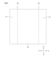
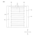
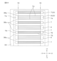
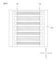
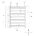
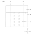
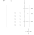
図1は、この発明の一実施形態に係る半導体装置の平面図であって、パッド部よりも上側の層が省略された平面図である。図2Aは、図1のA部の拡大平面図であって、パッド部よりも下方に配置された配線メタル構造を示す図である。図2Bは、図1のA部の拡大平面図であって、配線メタル構造よりも下方に配置された電極メタル構造を示す図である。 Figure 1 is a plan view of a semiconductor device according to one embodiment of the present invention, with layers above the pad portion omitted. Figure 2A is an enlarged plan view of part A in Figure 1, showing a wiring metal structure arranged below the pad portion. Figure 2B is an enlarged plan view of part A in Figure 1, showing an electrode metal structure arranged below the wiring metal structure.
半導体装置1は、平面視において矩形状に形成されている。説明の便宜上、以下において、図1、図2Aおよび図2Bに示した+X方向、-X方向、+Y方向および-Y方向を用いることがある。+X方向および-X方向は、平面視において、半導体装置1の表面の隣接する2つの辺のうちの一方の辺に沿う2つの方向であり、+Y方向および-Y方向は、他方の辺に沿う2つの方向である。+X方向および-X方向を総称するときには単に「X方向」という。+Y方向および-Y方向を総称するときには単に「Y方向」という。
The
半導体装置1は、半導体積層構造(窒化物半導体構造)2と、半導体積層構造2上に配置された電極メタル構造と、電極メタル構造上に配置された配線メタル構造と、配線メタル構造上に配置されたパッド部とを含む。
The
電極メタル構造は、図2Bに示すように、ソース電極3、ゲート電極4およびドレイン電極5を含む。ソース電極3およびドレイン電極5はX方向に延びている。ゲート電極4は、互いに平行にX方向に延びた複数の電極部81と、これらの複数の電極部81の対応する端部どうしをそれぞれ連結する2つのベース部82とを含む。
As shown in FIG. 2B, the electrode metal structure includes a
図2Bの例では、ソース電極3(S)、ゲート電極4の電極部81(G)およびドレイン電極5(D)は、Y方向にDGSGDGSの順に周期的に配置されている。これにより、ソース電極3(S)およびドレイン電極5(D)でゲート電極4の電極部81(G)を挟むことによって素子構造が構成されている。半導体積層構造2上の表面の領域は、当該素子構造を含むアクティブエリア16と、アクティブエリア16以外のノンアクティブエリア17とからなる。図2Aおよび図2Bにおいて、符号18は、アクティブエリア16とノンアクティブエリア17との境界線である素子分離線(isolation line)を示している。ゲート電極4のベース部82は、ノンアクティブエリア17において、複数の電極部81の対応する端部どうしをそれぞれ連結している。
2B, the source electrode 3 (S), the electrode portion 81 (G) of the
配線メタル構造は、図2Aに示すように、Y方向に延びたソース配線9(S)、ドレイン配線10(D)およびゲート配線11(G)を含む。図2Aの例では、X方向に離れて配置された2つのゲート配線11(G)の間に、ソース配線9(S)およびドレイン配線10(D)が交互に並んで配置されている。配線メタル構造のソース配線9(S)、ドレイン配線10(D)およびゲート配線11(G)は、電極メタル構造のソース電極3(S)、ゲート電極4の電極部81(G)およびドレイン電極5(D)と直交している。ソース配線9(S)、ドレイン配線10(D)およびゲート配線11(G)は、それぞれソース電極3(S)、ドレイン電極5(D)およびゲート電極4(G)に電気的に接続されている。
As shown in FIG. 2A, the wiring metal structure includes a source wiring 9 (S), a drain wiring 10 (D), and a gate wiring 11 (G) extending in the Y direction. In the example of FIG. 2A, the source wiring 9 (S) and the drain wiring 10 (D) are arranged alternately between two gate wirings 11 (G) arranged apart in the X direction. The source wiring 9 (S), the drain wiring 10 (D), and the gate wiring 11 (G) of the wiring metal structure are perpendicular to the source electrode 3 (S), the electrode portion 81 (G) of the
パッド部には、図1に示すように、ドレインパッド12、ソースパッド13、ゲートパッド14および基板コンタクト部15が配置されている。ドレインパッド12、ソースパッド13およびゲートパッド14は、それぞれドレイン配線10(D)、ソース配線9(S)およびゲート配線11(G)に電気的に接続されている。
As shown in FIG. 1, the pad section includes a
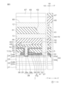
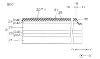
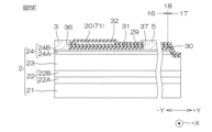
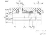
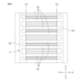
図3は、主として図2AのIII-III線に沿う断面を示す拡大断面図である。図3では、平面視において、ドレイン配線10が存在する領域において、図2Bのゲート電極41の1つの電極部81を含む小領域を+X方向から見た断面がアクティブエリア16として示されている。
Figure 3 is an enlarged cross-sectional view mainly showing a cross section along line III-III in Figure 2A. In Figure 3, in a plan view, in the region where the
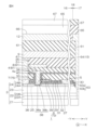
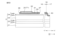
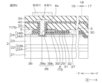
図4は、主として図2AのIV-IV線に沿う断面を示す拡大断面図である。図4では、平面視において、ソース配線9が存在する領域において、図2Bのゲート電極4の1つの電極部81を含む小領域を+X方向から見た断面がアクティブエリア16として示されている。また、図3および図4では、図1の基板コンタクト部15の一部を+X方向から見た断面がノンアクティブエリア17として示されている。
Figure 4 is an enlarged cross-sectional view mainly showing a cross section along line IV-IV in Figure 2A. In Figure 4, in a plan view, in the region where the
図3および図4を参照して、半導体積層構造2は、基板21と、基板21の表面に形成されたバッファ層22と、バッファ層22上にエピタキシャル成長された電子走行層23と、電子走行層23上にエピタキシャル成長された電子供給層24とを含む。
Referring to Figures 3 and 4, the
基板21は、たとえば、シリコン基板である。バッファ層22は、この実施形態では、基板21の表面に接するAlN膜からなる第1バッファ層22Aと、この第1バッファ層の表面(基板21とは反対側の表面)に積層されたAlGaN膜からなる第2バッファ層22Bとから構成されている。第1バッファ層22Aの膜厚は、例えば0.2μmであり、第2バッファ層22Bの膜厚は、例えば0.12μmである。バッファ層22は、たとえば、AlNの単膜から構成されていてもよい。
The
電子走行層23および電子供給層24は、互いにAl組成の異なる窒化物半導体からなる。この実施形態では、電子走行層23は、GaN層からなり、その厚さは0.1μm~3.0μm程度である。電子供給層24は、主として電子走行層23よりもAl組成の高い窒化物半導体からなっている。この実施形態では、電子供給層24は、電子走行層23上に形成されたAlN層24Aと、AlN層24A上に形成されたキャップ層24Bとからなる。AlN層24Aの厚さは、例えば2nm程度である。AlN層24Aは、AlN層に限らず、AlxInyGa1-x-yN(0.8≦x≦1.0,0≦x+y≦1)層から構成されていればよい。キャップ層24Bは、GaN層からなり、AlN層24Aの表面の粗さを低減するために設けられている。キャップ層24Bの膜厚は、1nm程度である。電子供給層24は、AlN層24Aのみから構成されていてもよい。
The
このように電子走行層23と電子供給層24とは、Al組成の異なる窒化物半導体からなっており、それらの間には格子不整合が生じている。具体的には、電子供給層24を主に構成しているAlNの格子定数は、電子走行層23を構成しているGaNの格子定数よりも小さい。このため、電子供給層24には、成長面に平行な方向に引っ張り歪が生じている。そして、電子走行層23および電子供給層24の自発分極ならびにそれらの間の格子不整合に起因するピエゾ分極によって、電子走行層23と電子供給層24との界面における電子走行層23の伝導帯のエネルギーレベルはフェルミ準位よりも低くなる。これにより、電子走行層23内の電子走行層23と電子走行層23との界面に近い位置(たとえば界面から数Å程度の距離)には、二次元電子ガス(2DEG)25が広がっている。
As described above, the
電子供給層24上には、パッシベーション膜29が形成されている。パッシベーション膜29は、SiN膜からなる。パッシベーション膜29の膜厚は、例えば6nm~25nm程度である。ノンアクティブエリア17においては、パッシベーション膜29の表面に、パッシベーション膜29および電子供給層24を貫通して電子走行層23の内部に達する凹部30が形成されている。
A
パッシベーション膜29上および凹部30の側壁および底壁上には、第1保護膜31、第2保護膜32、第1層間絶縁膜33、第2層間絶縁膜34および第3層間絶縁膜35が、その順番で形成されている。第1保護膜31は、パッシベーション膜29を覆っている。
第1保護膜31、第2保護膜32および第1層間絶縁膜33は、本願の装置発明の絶縁層に相当する。第2層間絶縁膜34は、本願の製造方法の発明における第1絶縁層に相当する。第3層間絶縁膜35は、本願の製造方法の発明における第2絶縁層に相当する。
A first
The first
この実施形態では、これらの各膜31~35は、SiO2膜からなる。第1保護膜31の厚さは、例えば40nm程度である。第2保護膜32の厚さは、例えば100nm程度である。第1層間絶縁膜33の厚さは、例えば600nm程度である。第2層間絶縁膜34の厚さは、例えば200nm程度である。第3層間絶縁膜35の厚さは、例えば500nm程度である。
In this embodiment, each of these
第2保護膜32、第1保護膜31およびパッシベーション膜29には、電子供給層24に達する、ソースコンタクトホール36およびドレインコンタクトホール37が形成されている。ソースコンタクトホール36およびドレインコンタクトホール37には、それぞれ、ソース電極3およびドレイン電極5が埋め込まれている。この実施形態では、ソース電極3およびドレイン電極4は、それぞれ、ソースコンタクトホール36およびドレインコンタクトホール37の周縁で第2保護膜32上に形成されたオーバーラップ部を含んでいる。ソース電極3およびドレイン電極5は、それぞれ、ソースコンタクトホール36およびドレインコンタクトホール37内で、電子供給層24にオーミック接触している。ソース電極3およびドレイン電極5は、X方向(図3および図4の紙面の厚さ方向)に延びている。
The second
ソース電極3およびドレイン電極5は、例えば、Ti膜、AlSiCu膜、Ti膜およびTiN膜が、下層からその順に積層されたTi/AlSiCu/Ti/TiN積層膜から構成されている。下層側のTi膜の厚さは、例えば20nmである。AlSiCu膜の厚さは、例えば2000nmである。上層側のTi膜の厚さは、例えば20nmである。TiN膜の厚さは、例えば50nmである。
The
ソース電極3とドレイン電極5との間位置において、第1層間絶縁膜33、第2保護膜32、第1保護膜31、パッシベーション膜29および電子供給層24には、電子走行層23に達するゲート開口部38が形成されている。ゲート開口部38は、第1層間絶縁膜33および第2保護膜32に形成された第1開口部38aと、第1保護膜31、パッシベーション膜29および電子供給層24に形成され、第1開口部38aに連通する第2開口部38bとを含む。第2開口部38bのうち電子供給層24を貫通している部分が、本願発明の下側開口部に相当する。また、第2開口部38bのうちパッシベーション膜29および第1保護膜31を貫通している部分と、第1開口部38aとによって、本願発明の上側開口部が構成されている。
Between the
ゲート開口部38の底部には、電子走行層23が露出している。ゲート開口部38の底壁および側壁を覆うようにゲート絶縁膜40が形成されている。ゲート絶縁膜40は、ゲート開口部38内に加えて、第1層間絶縁膜33と第2層間絶縁膜34との間にも形成されている。ゲート絶縁膜40は、例えば、SiO2膜からなる。ゲート絶縁膜40の厚さは、例えば、20nm程度である。
The
ゲート開口部38内にはゲート電極4が埋め込まれている。この実施形態では、ゲート電極4は、ゲート開口部38の周縁でゲート絶縁膜40上に形成されたオーバーラップ部4aを含んでいる。ゲート電極4の電極部81は、X方向(図3および図4の紙面の厚さ方向)に延びている。ゲート電極4は、例えば、TiN膜、W膜、AlCu膜およびTiN膜が、下層からその順に積層されたTiN/W/AlCu/TiN積層膜から構成されている。下層側のTiN膜の厚さは、例えば100nmである。W膜の厚さは、例えば500nmである。AlCu膜の厚さは、例えば500nmである。上層側のTiN膜の厚さは、例えば50nmである。
The
ゲート電極4の電極部81の両側には、ゲート開口部38の側部を部分的に形成するように、第1ソースフィールドプレート(第1SFP)6およびフローティングプレート7が配置されている。フローティングプレート7は、ソース電極3とゲート電極4の電極部81との間に配置されている。第1ソースフィールドプレート6は、ゲート電極4の電極部81とドレイン電極5との間に配置されている。
A first source field plate (first SFP) 6 and a floating
第1ソースフィールドプレート6およびフローティングプレート7は、ゲート開口部38の両側部の高さ中間位置で露出するように、第1保護膜31上に形成されている。つまり、ゲート開口部38の側部は、下側が第1保護膜31、パッシベーション膜29および電子供給層24によって形成され、中間部が第1ソースフィールドプレート6およびフローティングプレート7によって形成され、上側が第2保護膜32および第1層間絶縁膜33によって形成されている。
The first
フローティングプレート7および第1ソースフィールドプレート6に接するように、第1開口部38aの側部に絶縁性のサイドウォール39が形成されている。つまり、サイドウォール39は、第1開口部38aの側部とゲート絶縁膜40との間に配置されている。たとえば、サイドウォール39は、例えばSiO2膜からなり、その厚さは、例えば100nm程度である。
An insulating
フローティングプレート7および第1ソースフィールドプレート6は、サイドウォール39およびゲート絶縁膜40によって、ゲート電極4から絶縁されている。フローティングプレート7および第1ソースフィールドプレート6は、例えばTiN膜からなり、その厚さは、例えば100nm程度である。
The floating
第1ソースフィールドプレート6は、ソース電極3(ソース配線9)に電気的に接続されている。第1ソースフィールドプレート6は、よく知られているように、ゲート電極4の電極部81の端部への電界集中を緩和するために設けられている。一方、フローティングプレート7は、いずれの電極3,4,5にも電気的に接続されていない。
The first
第2層間絶縁膜34上には、平面視において、ゲート電極4の電極部81の上面に対向する位置に、第2ソースフィールドプレート(第2SFP)8が配置されている。第2ソースフィールドプレート8(正確には、後述する第2ソースフィールドプレート8の電極部91)は、X方向(図3および図4の紙面の厚さ方向)に延びている。第2ソースフィールドプレート8は、第3層間絶縁膜35によって覆われている。
A second source field plate (second SFP) 8 is disposed on the second
この実施形態では、第2ソースフィールドプレート8の幅は、ゲート電極4の電極部81の上面(オーバーラップ4aの上面を含む)の幅よりも大きい。平面視において、第2ソースフィールドプレート8の-Y方向側端は、ゲート電極4の電極部81の上面の-Y方向側端よりも、-Y方向に突出している。同様に、平面視において、第2ソースフィールドプレート8の+Y方向側端は、ゲート電極4の電極部81の上面の+Y方向側端よりも、+Y方向に突出している。第2ソースフィールドプレート8は、例えばTiN膜からなり、その厚さは、例えば100nm程度である。なお、平面視において、第2ソースフィールドプレート8の-Y方向側端および+Y方向側端は、それぞれ、ゲート電極4の電極部81の上面の-Y方向側端および+Y方向側端から外方に突出していなくてもよい。
In this embodiment, the width of the second
第2ソースフィールドプレート8は、ソース電極3(ソース配線9)に電気的に接続されている。第2ソースフィールドプレート8は、帰還容量Crss(=ゲート・ドレイン間の静電容量Cgd)を低減することにより、半導体装置1のスイッチング特性を向上させるために設けられている。第2ソースフィールドプレート8が設られている理由の詳細については、後述する。
The second
第3層間絶縁膜35、第2層間絶縁膜34、ゲート絶縁膜40および第1層間絶縁膜33には、ソース電極3およびドレイン電極5にそれぞれ達する、第1ソースビアホール41および第1ドレインビアホール42(図3、図4、図6O参照)が形成されている。第1ソースビアホール41および第1ドレインビアホール42には、それぞれ、ソースビアメタル51およびドレインビアメタル52(図3、図4、図6P参照)が埋め込まれている。ソースビアメタル51およびドレインビアメタル52は、それぞれ、第1ソースビアホール41および第1ドレインビアホール42内で、ソース電極3およびドレイン電極5に電気的に接続されている。
The third
図3および図4には図示されていないが、第3層間絶縁膜35、第2層間絶縁膜34、ゲート絶縁膜40、第1層間絶縁膜33および第2保護膜32には、第1ソースフィールドプレート6に達する、第1SFP用ビアホール44(図6O参照)が形成されている。第1SFP用ビアホール44には、第1SFP用ビアメタル54(図6P参照)が埋め込まれている。第1SFP用ビアメタル54は、第1SFP用ビアホール44内で、第1ソースフィールドプレート6に電気的に接続されている。
3 and 4, a first SFP via hole 44 (see FIG. 6O) is formed in the third
図3および図4には図示されていないが、第3層間絶縁膜35および第2層間絶縁膜34には、ゲート電極4に達する、第1ゲートビアホール43(図6O参照)が形成されている。第1ゲートビアホール43には、ゲートビアメタル53(図6P参照)が埋め込まれている。ゲートビアメタル53は、第1ゲートビアホール43内で、ゲート電極4に電気的に接続されている。
Although not shown in Figures 3 and 4, a first gate via hole 43 (see Figure 6O) that reaches the
図3および図4には図示されていないが、第3層間絶縁膜35には、第2ソースフィールドプレート8に達する、第2SFP用ビアホール45(図6O参照)が形成されている。第2SFP用ビアホール45には、第2SFP用ビアメタル55(図6P参照)が埋め込まれている。第2SFP用ビアメタル55は、第2SFP用ビアホール45内で、第2ソースフィールドプレート8に電気的に接続されている。
Although not shown in FIGS. 3 and 4, a second SFP via hole 45 (see FIG. 6O) is formed in the third
第3層間絶縁膜35上には、X方向に間隔をおいて、ソース配線9、ドレイン配線10およびゲート配線11が形成されている。ソース配線9、ドレイン配線10およびゲート配線11は、Y方向に延びている。図3の断面図には、第3層間絶縁膜35上に形成されたドレイン配線10が現れている。図4の断面図には、第3層間絶縁膜35上に形成されたソース配線9が現れている。
On the third
図3および図6Pに示すように、ドレイン配線10には、ドレインビアメタル52が接続されている。また、図4および図6Pに示すように、ソース配線9には、ソースビアメタル51が接続されている。図4には図示されていないが、図6Pに示すように、ソース配線9には、第1SFP用ビアメタル54および第2SFP用ビアメタル55が接続されている。図3および図4には図示されていないが、図6Pに示すように、ゲート配線11には、ゲートビアメタル53が接続されている。各ビアメタル51~55は、対応するビアホール41~45の側壁に形成されるTiNバリア膜と、TiNバリア膜の内側に埋め込まれるW(タングステン)とからなる。
As shown in FIG. 3 and FIG. 6P, a drain via
ソース配線9、ドレイン配線10およびゲート配線11は、例えば、TiN膜、AlCu膜およびTiN膜が第3層間絶縁膜35上に順に積層されたTiN/AlCu/TiN積層膜からなる。各TiN膜の厚さは、例えば40nm程度であり、AlCu膜の厚さは、例えば1000nm程度である。
The
第3層間絶縁膜35上には、ソース配線9、ドレイン配線10およびゲート配線11を覆う第4層間絶縁膜61が形成されている。第4層間絶縁膜61は、例えばSiO2からなり、その厚さは例えば1000nm程度である。第4層間絶縁膜61の所要箇所には、図3に示すように、ドレイン配線10に達する第2ドレインビアホール62が形成されている。図3および図4には図示されていないが、第4層間絶縁膜61の所要箇所には、ソース配線9に達する第2ソースビアホールおよびゲート配線11に達する第2ゲートビアホールが形成されている。
A fourth
第4層間絶縁膜61上には、図3および図4に示すように、ドレインパッド12が形成されている。ドレインパッド12は、第2ドレインビアホール62に入りこみ、第2ドレインビアホール62内でドレイン配線10に接続されている。図3および図4には図示されていないが、第4層間絶縁膜61上には、図1に示されるソースパッド13およびゲートパッド14が形成されている。ソースパッド13は、第2ソースビアホールに入りこみ、第2ソースビアホール内でソース配線9に接続されている。ゲートパッド14は、第2ゲートビアホールに入りこみ、第2ゲートビアホール内でゲート配線11に接続されている。ドレインパッド12、ソースパッド13およびゲートパッド14は、例えば、下層のTiN層と上層のAlCu層とのTiN/AlCu積層膜からなる。TiN層の厚さは、例えば40nm程度であり、AlCu層の厚さは、例えば4200nm程度である。
As shown in FIG. 3 and FIG. 4, the
ノンアクティブエリア17(基板コンタクト部15を含むノンアクティブエリア)においては、第4層間絶縁膜61、第3層間絶縁膜35、第2層間絶縁膜34、ゲート絶縁膜40、第1層間絶縁膜33、第2保護膜32、第1保護膜31、電子走行層23およびバッファ層22に、基板21に達する基板コンタクトホール63が形成されている。基板コンタクトホール63は、第4層間絶縁膜61、第3層間絶縁膜35、第2層間絶縁膜34、ゲート絶縁膜40、第1層間絶縁膜33、第2保護膜32および第1保護膜31に形成された第1基板コンタクトホール63aと、電子走行層23およびバッファ層22に形成されかつ第1基板コンタクトホール63aに連通する第2基板コンタクトホール63bとからなる。
In the non-active area 17 (non-active area including the substrate contact portion 15), a
基板コンタクトホール63内に基板コンタクトメタル64が埋め込まれることにより、基板コンタクト部15が形成されている。基板コンタクトメタル64の材料は、例えば、ドレインパッド12、ソースパッド13およびゲートパッド14の材料と同じである。
第4層間絶縁膜61上には、ドレインパッド12、ソースパッド13およびゲートパッド14および基板コンタクト部15(基板コンタクトメタル64)を覆う第3保護膜65が形成されている。第3保護膜65は、例えば、下層のSiO2膜と上層のSiN膜とからなるSiO2/SiN積層膜からなる。SiO2膜の厚さは、600nm程度であり、SiN膜の厚さは600nm程度である。
A third
第3保護膜65には、図3および図4に示すように、ドレインパッド12の中央部を露出させるためのドレインパッド開口部66が形成されている。図3および図4には、図示されていないが、ソースパッド13の中央部を露出させるためのソースパッド開口部およびゲートパッド14の中央部を露出させるためのゲートパッド開口部が形成されている。
As shown in Figures 3 and 4, a
第3保護膜65の表面には、樹脂層67が形成されている。樹脂層67は、例えばポリイミド層からなり、その厚さは、例えば10μm程度である。
A
この半導体装置1では、電子走行層23上にAl組成の異なる電子供給層24が形成されてヘテロ接合が形成されている。これにより、電子走行層23と電子供給層24との界面付近の電子走行層23内に二次元電子ガス25が形成され、この二次元電子ガス25をチャネルとして利用したHEMTが形成されている。
In this
ゲート電極4の電極部81は、ゲート絶縁膜40を挟んで電子走行層23に対向しており、ゲート電極4の電極部81の直下には、電子供給層24は存在しない。したがって、ゲート電極4の電極部81の直下では、電子供給層24と電子走行層23との格子不整合による分極に起因する二次元電子ガス25が形成されない。よって、ゲート電極4にバイアスを印加していないとき(ゼロバイアス時)には、二次元電子ガス25によるチャネルはゲート電極4の電極部81の直下で遮断されている。こうして、ノーマリーオフ型のHEMTが実現されている。ゲート電極4に適切なオン電圧(たとえば5V)を印加すると、ゲート電極4の電極部81の直下の電子走行層23内にチャネルが誘起され、ゲート電極4の電極部81の両側の二次元電子ガス25が接続される。これにより、ソース-ドレイン間が導通する。
The
使用に際しては、たとえば、ソース電極3とドレイン電極5との間に、ドレイン電極5側が正となる所定の電圧(たとえば200V~400V)が印加される。その状態で、ゲート電極4に対して、ソース電極3を基準電位(0V)として、オフ電圧(0V)またはオン電圧(5V)が印加される。
When in use, for example, a predetermined voltage (e.g., 200 V to 400 V) is applied between the
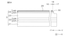
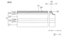
図5A~図5Xは、前述の半導体装置1の製造工程の一例を説明するための断面図である。図5A~図5Xの断面は、図3の切断面に対応する断面図である。図6A~図6Vは、前述の半導体装置1の製造工程の一例を説明するための平面図である。図6A~図6Vの平面図は、図1のA部の平面図である。
Figures 5A to 5X are cross-sectional views for explaining an example of a manufacturing process of the
半導体装置1を製造するには、図5Aおよび図6Aに示すように、基板21上に、バッファ層22(22A,22B)および電子走行層23が順にエピタキシャル成長される。次に、電子走行層23上に電子供給層24(24A,24B)がエピタキシャル成長される。
To manufacture the
次に、電子供給層24上の全面を覆うように、例えばCVD法(化学的気相成長法)によって、パッシベーション膜29が形成される。この実施形態では、パッシベーション膜29は、バッファ層22、電子走行層23および電子供給層24が成膜された成膜装置内で成膜される。この後、ノンアクティブエリア17において、パッシベーション膜29、バッファ層22、電子走行層23および電子供給層24の表層部がエッチングされることにより、凹部30が形成される。
Next, a
次に、図5Bおよび図6Bに示すように、パッシベーション膜29上の全面および凹部30の内面を覆うように、例えばLPCVD法(減圧CVD法)によって、第1保護膜31が形成される。
Next, as shown in Figures 5B and 6B, a first
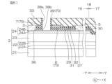
次に、例えばスパッタ法によって、第1保護膜31上にプレート膜が形成された後、例えばドライエッチングによって、プレート膜が選択的に除去される。これにより、図5Cおよび図6Cに示すように、第1保護膜31上にプレート膜20が形成される。プレート膜20は、互いに平行にかつX方向に延びる複数の電極部71と、複数の電極部71の対応する端部どうしをそれぞれ連結する2つのベース部72とを含んでいる。各ベース部72のX方向の外側縁部は、それぞれノンアクティブエリア17に配置されている。Y方向両端にある電極部71を除いて、各電極部71は、ソース電極3の形成予定領域とドレイン電極5の形成予定領域との間に形成される。
Next, a plate film is formed on the first
次に、図5Dおよび図6Dに示すように、第1保護膜31上の全面を覆うように、例えばPECVD法(プラズマCVD法)によって、第2保護膜32が形成される。これにより、プレート膜20は、第1保護膜31と第2保護膜32とからなる保護膜内に埋め込まれる。この後、ソース電極3の形成予定領域およびドレイン電極4の形成予定領域において、第2保護膜32、第1保護膜31およびパッシベーション膜29がエッチングされることによって、ソースコンタクトホール36およびドレインコンタクトホール37が形成される。
Next, as shown in FIG. 5D and FIG. 6D, a second
次に、図5Eおよび図6Eに示すように、ソースコンタクトホール36内およびドレインコンタクトホール37内に、それぞれソース電極3およびドレイン電極5が埋め込まれる。前述したように、この実施形態では、ソース電極3およびドレイン電極5は、それぞれ、ソースコンタクトホール36およびドレインコンタクトホール37の周縁で第2保護膜32上に形成されたオーバーラップ部を含む。
Next, as shown in Figures 5E and 6E, the
次に、図5Fおよび図6Fに示すように、第2保護膜32、ソース電極3およびドレイン電極5を覆うように、例えばCVD法によって、第1層間絶縁膜33が形成される。
Next, as shown in Figures 5F and 6F, a first
次に、図5Gおよび図6Gに示すように、プレート膜20に対向するエッチング領域から、第1層間絶縁膜33、第2保護膜32およびプレート膜20をエッチングすることによって、ゲート開口部38における第1開口部38aが形成される。これにより、プレート膜20は、ゲート開口部38に対して自己整合的に、ドレイン側の第1ソースフィールドプレート6とソース側のフローティングプレート7とに分離される。したがって、第1ソースフィールドプレート6とフローティングプレート7は、この段階では、ゲート開口部38の側部に露出することになる。
Next, as shown in Figures 5G and 6G, the first
ソースフィールドプレート6は、図6Gに示すように、ドレイン電極5を挟んでX方向に互いに平行に延びた一対の電極部73と、ノンアクティブエリア17において、これらの一対の電極部73の対応する端部どうしをそれぞれ連結する2つのベース部74とを含む。フローティングプレート7は、図6Gに示すように、ソース電極3を挟んでX方向に互いに平行に延びた一対の電極部75と、ノンアクティブエリア17において、これらの一対の電極部75の対応する端部どうしをそれぞれ連結する2つのベース部76とを含む。
As shown in FIG. 6G, the
次に、第1層間絶縁膜33上の全面および第1開口部38aの内面(側壁および底壁)を覆うように、例えば、CVD法によって、サイドウォール39の材料膜(SiO2膜)が形成される。そして、この材料膜がドライエッチングされることにより、この材料膜における第1層間絶縁膜33上の部分および第1開口部38aの底壁上の部分が選択的に除去され、図5Hおよび図6Hに示すように、第1開口部38aの側壁にサイドウォール39の材料膜70が形成される。ただし、図6Hにおいては、サイドウォール39の材料膜70は省略されている。このため、図6Hは図6Gと同じ図となっている。
Next, a material film ( SiO2 film) of the
次に、図5Iおよび図6Iに示すように、ドライエッチングによって、第1開口部38a直下の第1保護膜31およびパッシベーション膜29が選択的に除去される。これにより、アクティブエリア16において、第1保護膜31およびパッシベーション膜29に電子供給層24に達する開口(第2開口部38bの一部)が形成されるとともに、図6Iに示されるノンアクティブエリア17において、第1保護膜31に電子走行層23に達する開口が形成される。また、材料膜70が薄膜化されることにより、第1開口部38aの側壁にサイドウォール39が形成される。
Next, as shown in Figures 5I and 6I, the first
以下の説明に用いられる図6J~図6Oにおいては、説明の便宜上、それよりも上層の部材によって平面図には現れない部分が、破線ではなく実線が表示されることがある。 In Figures 6J to 6O used in the following explanation, for ease of explanation, parts that do not appear in the plan view due to components in upper layers may be shown with solid lines instead of dashed lines.
次に、図5Jおよび図6Jに示すように、アクティブエリア16において、AlN酸化処理およびウエットエッチングによって、第1開口部38a直下の電子供給層24(24A,24B)が選択的に除去される。これにより、アクティブエリア16において、第1保護膜31、パッシベーション膜29および電子供給層24に、電子走行層23に達する第2開口部38bが形成される。これにより、第1開口部38aと第2開口部38bとからなるゲート開口部38が形成される。
Next, as shown in Figures 5J and 6J, in the
次に、図5Kおよび図6Kに示すように、ゲート開口部38の内面および第1層間絶縁膜33上の全面を覆うように、例えばCVD法によって、ゲート絶縁膜40が形成される。
Next, as shown in Figures 5K and 6K, a
次に、図5Lおよび図6Lに示すように、ゲート開口部38内のゲート絶縁膜40の内側に、ゲート電極4が埋め込まれる。ゲート電極4は、図6Lに示すように、互いに平行にX方向に延びた複数の電極部81と、ノンアクティブエリア17において、これらの複数の電極部81の対応する端部どうしをそれぞれ連結する2つのベース部82とを含む。前述したように、この実施形態では、ゲート電極4は、ゲート開口部38の周縁でゲート絶縁膜40上に形成されたオーバーラップ部4aを含む。
Next, as shown in Figures 5L and 6L, the
次に、図5Mおよび図6Mに示すように、ゲート絶縁膜40上の全面およびゲート電極4を覆うように、例えばCVD法によって、第2層間絶縁膜34が形成される。
Next, as shown in Figures 5M and 6M, a second
次に、例えばスパッタ法によって、第2層間絶縁膜34上に第2ソースフィールドプレート8の材料であるプレート膜が形成された後、ドライエッチングによって、プレート膜が選択的に除去される。これにより、図5Nおよび図6Nに示すように、第2層間絶縁膜34上に第2ソースフィールドプレート8が形成される。第2ソースフィールドプレート8は、図6Nに示すように、互いに平行にX方向に延びた複数の電極部91と、ノンアクティブエリア17において、これらの複数の電極部91の対応する端部どうしをそれぞれ連結する2つのベース部92とを含む。
Next, a plate film, which is the material of the second
次に、図5Oおよび図6Oに示すように、第2層間絶縁膜34上の全面および第2ソースフィールドプレート8を覆うように、例えばCVD法によって、第3層間絶縁膜35が形成される。その後、図6Oに示すように、例えばエッチングによって、複数の第1ソースビアホール41、複数の第1ドレインビアホール42、複数の第1ゲートビアホール43、複数の第1SFP用ビアホール44および複数の第2SFP用ビアホール45が形成される。
Next, as shown in Figures 5O and 6O, a third
第1ソースビアホール41は、アクティブエリア16において、ソース電極3と第3層間絶縁膜35上に形成されるソース配線9とが対向する領域において、それらの間の絶縁膜33,40,34,35を貫通するように形成される。第1ドレインビアホール42は、アクティブエリア16において、ドレイン電極5と第3層間絶縁膜35上に形成されるドレイン配線10とが対向する領域において、それらの間の絶縁膜33,40,34,35を貫通するように形成される。第1ゲートビアホール43は、ノンアクティブエリア17において、ゲート電極4のベース部82(図6L参照)と第3層間絶縁膜35上に形成されるゲート配線11とが対向する領域において、それらの間の絶縁膜40,34,35を貫通するように形成される。
The first source via
第1SFP用ビアホール44は、ノンアクティブエリア17において、第1ソースフィールドプレート6のベース部74(図6G参照)と第3層間絶縁膜35上に形成されるソース配線9とが対向する領域において、それらの間の絶縁膜32,33,40,34,35を貫通するように形成される。第2SFP用ビアホール45は、ノンアクティブエリア17において、第2ソースフィールドプレート8のベース部92(図6N参照)と第3層間絶縁膜35上に形成されるソース配線9とが対向する領域において、それらの間の絶縁膜35を貫通するように形成される。
The first SFP via
次に、図5Pおよび図6Pに示すように、各ビアホール41、42、43、44および45に、それぞれビアメタル51、52、53、54および55が埋め込まれる。そして、第3層間絶縁膜35上に、例えばスパッタ法によって、ソース配線9、ドレイン配線10およびゲート配線11が形成される。図6Pに示すように、ソースビアメタル51は、ソース配線9に接続される。ドレインビアメタル52は、ドレイン配線10に接続される。ゲートビアメタル53は、ゲート配線11に接続される。第1SFP用ビアメタル54および第2SFP用ビアメタル55は、ソース配線9に接続される。
Next, as shown in FIG. 5P and FIG. 6P, via
次に、図5Qおよび図6Qに示すように、第3層間絶縁膜35上の全面ならびにソース配線9、ドレイン配線10およびゲート配線11を覆うように、例えばCVD法によって、第4層間絶縁膜61が形成される。
Next, as shown in Figures 5Q and 6Q, a fourth
次に、図5Rに示すように、ノンアクティブエリア17において、例えばエッチングによって、第4層間絶縁膜61、第3層間絶縁膜35、第2層間絶縁膜34、ゲート絶縁膜40、第1層間絶縁膜33、第2保護膜32および第1保護膜31が選択的に除去されることにより、第1基板コンタクトホール63aが形成される。
Next, as shown in FIG. 5R, in the
次に、図5Sに示すように、ノンアクティブエリア17において、例えばエッチングによって、電子走行層23およびバッファ層22が選択的に除去されることにより、第1基板コンタクトホール63aに連通しかつ基板21に達する第2基板コンタクトホール63bが形成される。これにより、第1基板コンタクトホール63aおよび第2基板コンタクトホール63bからなる基板コンタクトホール63が形成される。
Next, as shown in FIG. 5S, in the
次に、図5Tおよび図6Rに示すように、平面視でドレインパッド12が形成されるべき領域内において、第4層間絶縁膜61に、ドレイン配線10に達する複数の第2ドレインビアホール62が形成される。この際、平面視でソースパッド13が形成されるべき領域において、第4層間絶縁膜61に、ソース配線9に達する複数の第2ソースビアホール(図示略)が形成される。また、この際、平面視でゲートパッド14が形成されるべき領域において、第4層間絶縁膜61に、ゲート配線11に達する複数の第2ゲートビアホール(図示略)が形成される。
Next, as shown in Figures 5T and 6R, in the region where the
次に、図5Uおよび図6Sに示すように、第4層間絶縁膜61上に、ドレインパッド12、ソースパッド13およびゲートパッド14が形成されるとともに、基板コンタクトホール63内に基板コンタクトメタル64が埋め込まれる。ドレインパッド12は、第2ドレインビアホール62を介してドレイン配線10に接続される。ソースパッド13は、第2ソースビアホールを介してソース配線9に接続される。ゲートパッド14は、第2ゲートビアホールを介してゲート配線11に接続される。
Next, as shown in Figures 5U and 6S, the
次に、図5Vおよび図6Tに示すように、第4層間絶縁膜61上の全面、各パッド12,13,14および基板コンタクトメタル64を覆うように、例えばCVD法によって、第3保護膜65が形成される。
Next, as shown in Figures 5V and 6T, a third
次に、図5Wおよび図6Uに示すように、第3保護膜65に、ドレインパッド12、ソースパッド13およびゲートパッド14をそれぞれ露出させるドレインパッド開口部66、ソースパッド開口部およびゲートパッド開口部が形成される。
Next, as shown in Figures 5W and 6U, a
次に、図5Xおよび図6Vに示すように、第3保護膜65の表面に、例えばCVD法によって、樹脂層67が形成される。以上の工程を経て、図1~図4に示す半導体装置1が得られる。
Next, as shown in Figures 5X and 6V, a
以下、第2ソースフィールドプレート8が設けられている理由について説明する。
The reason why the second
以下において、前述の実施形態の半導体装置1に対して、第2ソースフィールドプレート8が設けられていない点のみが異なる半導体装置を比較例ということにする。実施形態の半導体装置1および比較例に形成されているHEMTには、静電容量CGD,CGS、CDSが存在する。CGDは、HEMTのゲート・ドレイン間の静電容量(以下、ゲート・ドレイン間容量CGDという)であり、帰還容量Crssと呼ばれる。CGSは、HEMTのゲート・ソース間の静電容量(以下、ゲート・ソース間容量CGSという)である。CDSは、HEMTのドレイン・ソース間の静電容量(以下、ドレイン・ソース間容量CDSという)である。また、ゲート・ドレイン間容量CGDとゲート・ソース間容量CGSとの和(CGD+CGS)は、入力容量Cissと呼ばれる。また、ドレイン・ソース間容量CDSとゲート・ドレイン間容量CGDとの和(CDS+CGD)は、出力容量Cossと呼ばれる。
Hereinafter, a semiconductor device that differs from the
実施形態の半導体装置1および比較例において、ドレイン電極5と、ゲート電極4と、それらの間の電子供給層24および電子走行層23とによって、第1のゲート・ドレイン間容量CGD1が形成されている。実施形態の半導体装置1および比較例では、電極メタル構造におけるゲート電極4の電極部81と配線メタル構造のドレイン配線10とは直交して配置されている。このため、ゲート電極4の電極部81の長さ方向位置によっては、ゲート電極4の電極部81の真上にドレイン配線10が配置されることになる。ゲート電極4の電極部81の真上にドレイン配線10が配置されている部分には、ゲート電極4の電極部81とドレイン配線10とそれらの間の絶縁膜34,35とによって、第2のゲート・ドレイン間容量CGD2が形成される可能性がある。そうすると、第1のゲート・ドレイン間容量CGD1と第2のゲート・ドレイン間容量CGD2との和(CGD1+CGD2)が帰還容量Crss(ゲート・ドレイン間容量CGD)となるため、帰還容量Crssが大きくなるおそれがある。
In the
比較例のドレイン電圧に対する入力容量Ciss(=CGD+CGS)、出力容量Coss(=CDS+CGD)および帰還容量Crss(=CGD1+CGD2)の変化をシミュレーションによって推定した。 The changes in the input capacitance Ciss (=C GD +C GS ), the output capacitance Coss (=C DS +C GD ), and the feedback capacitance Crss (=C GD1 +C GD2 ) with respect to the drain voltage in the comparative example were estimated by simulation.
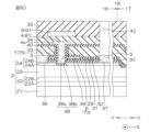
図7は、比較例のシミュレーションモデルM1を示す模式図である。図7において、図3の各部に対応する部分には、図3と同じ符号を付して示す。 Figure 7 is a schematic diagram showing a simulation model M1 of a comparative example. In Figure 7, parts corresponding to those in Figure 3 are denoted by the same reference numerals as in Figure 3.
図8は、シミュレーション結果を示すグラフである。 Figure 8 is a graph showing the simulation results.
図8に示すように、帰還容量Crssは、ドレイン電圧が大きくなるにしたがって低下し、その後、ほぼ一定となる。ドレイン電圧を上昇させた場合、初期において帰還容量Crssが低下するのは、電子供給層24および電子走行層23におけるゲート電極4の近傍に空乏層が広がるので、第1のゲート・ドレイン間容量CGD1が低下するためである。その後において、帰還容量Crssがさほど低下しないのは、第2のゲート・ドレイン間容量CGD2が存在するためである。
8, the feedback capacitance Crss decreases as the drain voltage increases, and then becomes approximately constant. When the drain voltage is increased, the feedback capacitance Crss decreases initially because a depletion layer spreads in the
このように比較例では、第2のゲート・ドレイン間容量CGD2が存在するため、帰還容量Crssが大きくなり、HEMTのスイッチング特性を悪化させるおそれがある。 As described above, in the comparative example, since the second gate-drain capacitance C GD2 exists, the feedback capacitance Crss increases, which may deteriorate the switching characteristics of the HEMT.
帰還容量Crssが大きくなると、HEMTのスイッチング特性が悪化することについて説明する。 This explains how an increase in feedback capacitance Crss leads to a deterioration in the switching characteristics of a HEMT.
図9Aは、半導体装置1に形成されたHEMT100と静電容量CGD,CGS,CDSを示す電気回路図である。
FIG. 9A is an electric circuit diagram showing the
半導体装置1に形成されたHEMT100のゲートGとドレインDとの間には、ゲート・ドレイン間容量CGDが存在する。HEMT100のゲートGとソースSとの間には、ゲート・ソース間容量CGSが存在する。HEMT100のドレインDとソースSとの間には、ドレイン・ソース間容量CDSが存在する。
A gate-drain capacitance C GD exists between the gate G and drain D of the
HEMT100がオフ状態である場合には、ゲートGおよびソースSの電位が0Vであり、ドレインDに所定の正電圧が印加されているので、ゲート・ドレイン間容量CGDおよびドレイン・ソース間容量CDSが図9Aに示すように充電される。ゲートGおよびソースSは同電位であるため、ゲート・ソース間容量CGSは充電されない。
When the
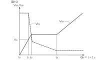
図10は、ゲートGにゲート電圧を印加した場合における、入力ゲート電荷量QG(=ゲート電流IG×時間t)に対する、ゲート・ソース間電圧VGSおよびドレイン・ソース間電圧VDSの変化を示すグラフである。 FIG. 10 is a graph showing changes in gate-source voltage V GS and drain-source voltage V DS with respect to the input gate charge Q G (=gate current I G ×time t) when a gate voltage is applied to gate G.
t0~t1期間:時刻t0でゲート電圧がゲートGに印加されると、図9Bに示すように、ゲート電流IGによってゲート・ソース間容量CGSの充電が開始されるので、ゲート・ソース間電圧VGSが上昇する。 Period t0 to t1: When a gate voltage is applied to the gate G at time t0, the gate current I G starts charging the gate-source capacitance C GS as shown in FIG. 9B, and the gate-source voltage V GS rises.
t1~t2期間:時点t1でゲート・ソース間電圧VGSが閾値電圧Vthに達すると、ドレイン・ソース間が短絡状態への遷移を開始するので、ドレイン・ソース間電圧VDSの低下が開始され、ドレイン・ソース間容量CDSの放電が開始される。 Period t1 to t2: When the gate-source voltage VGS reaches the threshold voltage Vth at time t1, the drain-source starts to transition to a short-circuited state, so the drain-source voltage VDS starts to decrease and the drain-source capacitance CDS starts to discharge.
t2~t3期間:ゲート・ドレイン間容量CGDは、ドレイン・ソース間電圧VDSが低下して、VGS≧VDSの状態となって初めて放電を開始する。ドレイン・ソース間電圧VDSが高いままだと、ゲート電流IGの流入によってゲート・ソース間電圧VGSが上昇しても、ゲート・ドレイン間容量CGDから見てHEMT100のオフ状態と同じくVGS<VDSのままであるためである。時点t2において、VGS≧VDSの状態となるので、図9Cに示すように、ゲート・ドレイン間容量CGDは、放電を開始する。そして、ゲート・ドレイン間容量CGDの放電が終了すると、ゲート・ドレイン間容量CGDはオフ状態での充電とは逆極性で充電され始める。
Period t2 to t3: The gate-drain capacitance C GD starts discharging only when the drain-source voltage V DS drops and V GS ≧V DS is satisfied. If the drain-source voltage V DS remains high, even if the gate-source voltage V GS rises due to the inflow of the gate current I G , V GS <V DS remains the same as when the
ゲート・ドレイン間容量CGDの放電開始から、ゲート・ドレイン間容量CGDのオフ状態での充電とは逆極性での充電が完了するまでの間、ゲート・ドレイン間容量CGDの放充電にゲート電流IGが消費されるため、ゲート・ソース間電圧VGSはほとんど変化しない。 From the start of discharging the gate-drain capacitance C GD until charging of the gate-drain capacitance C GD with the opposite polarity to that of the gate-drain capacitance C GD in the off state is completed, the gate current I G is consumed in charging and discharging the gate-drain capacitance C GD, so the gate-source voltage V GS hardly changes.
t3以降の期間:図9Dに示すように、ゲート・ソース間容量CGSのオフ状態での充電とは逆極性での充電が完了した後、つまり、入力容量(CGD+CGS)の充電が完了した後は、流入するゲート電流IGによって充電レベルが上がっていくので、ゲート・ソース間電圧VGSは時間に対してリニアに上昇する。 Period after t3: As shown in FIG. 9D, after charging of the gate-source capacitance CGS with the polarity opposite to that in the off state is completed, that is, after charging of the input capacitance ( CGD + CGS ) is completed, the charge level increases due to the inflowing gate current I , and the gate-source voltage VGS increases linearly with time.
ゲート・ドレイン間容量CGD(帰還容量Crss)が大きいと、時点t2~t3の期間が長くなるため、HEMT100のスイッチング特性が悪くなる。
If the gate-drain capacitance C GD (feedback capacitance Crss) is large, the period from time t2 to time t3 becomes long, and the switching characteristics of the
そこで、この実施形態では、ゲート電極4の電極部81上に、第2ソースフィールドプレート8を配置している。つまり、ゲート電極4の電極部81とドレイン配線10との間に、第2ソースフィールドプレート8を配置している。この第2ソースフィールドプレート8によって、ドレイン配線10とゲート電極4の電極部81との間の電気力線の少なくとも一部を遮断するようにしている。これにより、ゲート電極4の電極部81とドレイン配線10とそれらの間の絶縁膜34,35とによって形成される第2のゲート・ドレイン間容量CGD2を低減している。これにより、帰還容量Crssを低減することができるので、HEMT100のスイッチング特性を向上させることができる。
Therefore, in this embodiment, the second
第2のゲート・ドレイン間容量CGD2を低減するためには、平面視において、ゲート電極4の電極部81の上面に対向して配置される第2ソースフィールドプレート8の幅(Y方向長さ)は、ゲート電極4の電極部81の上面の幅(Y方向長さ)よりも大きく形成することが好ましい。そして、第2ソースフィールドプレート8の-Y方向側縁は、ゲート電極4の電極部81の上面の-Y方向側縁よりも、-Y方向に突出し、第2ソースフィールドプレート8の+Y方向側縁は、ゲート電極4の電極部81の上面の+Y方向側縁よりも、+Y方向に突出していることが好ましい。
In order to reduce the second gate-drain capacitance C GD2 , it is preferable that the width (length in the Y direction) of the second
このようにすると、第2ソースフィールドプレート8の幅(Y方向長さ)が、ゲート電極4の電極部81の上面の幅と同じで、かつ、第2ソースフィールドプレート8のY方向の両側縁がゲート電極4の電極部81の上面の両側縁から外方に突出していない構造に比べて、ドレイン配線10とゲート電極4の電極部81との間の電気力線をより効果的に遮断できるからである。
In this way, the width (length in the Y direction) of the second
実施形態の半導体装置1の入力容量Ciss、出力容量Cossおよび帰還容量Crssと、比較例の入力容量Ciss、出力容量Cossおよび帰還容量Crssとをシミュレーションによって計算した。
The input capacitance Ciss, output capacitance Coss, and feedback capacitance Crss of the
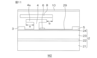
図11は、実施形態の半導体装置1のシミュレーションのモデルM2を示す模式図である。図11において、図3の各部に対応する部分には、図3と同じ符号を付して示す。図11において、aは、ゲート電極4のオーバーラップ部4aの幅(Y方向の長さ)を示している。このモデルM2では、aは、0.8μmに設定されている。図11において、bは、平面視において、ゲート電極4の電極部81の上面(オーバーラップ部4aの上面を含む)の+Y方向側縁からの、第2ソースフィールドプレート8の+Y方向側縁の突出量を示している。ゲート電極4の電極部81の上面の-Y方向側縁からの、第2ソースフィールドプレート8の-Y方向側縁の突出量は、ゲート電極4のオーバーラップ部4Aの+Y方向側縁からの、第2ソースフィールドプレート8の+Y方向側縁の突出量bと同じである。ここでは、突出量bは0.6μmに設定されている。
Figure 11 is a schematic diagram showing a model M2 of a simulation of the
ここでは、図11のモデルM2から、第2ソースフィールドプレート8を除去した構成を、比較例のシミュレーションのモデルとした。
Here, the model for the comparative example simulation was a configuration in which the second
図12は、シミュレーション結果を示す表である。各容量Ciss、CossおよびCrssは、ドレイン・ソース間電圧Vdsが50Vのときの容量(pF)である。図12から、第2ソースフィールドプレート8を有する実施形態の半導体装置1の方が、第2ソースフィールドプレート8を有していない比較例に比べて、帰還容量Crssが大幅に小さくなっていることがわかる。
Figure 12 is a table showing the simulation results. Each capacitance Ciss, Coss, and Crss is the capacitance (pF) when the drain-source voltage Vds is 50 V. From Figure 12, it can be seen that the feedback capacitance Crss is significantly smaller in the
前述の実施形態では、ゲート電極4はオーバーラップ部4aを有しているが、ゲート電極4はオーバーラップ部4aを有していなくてもよい。ゲート電極4はオーバーラップ部4aを有していない場合において、ゲート電極4の電極部81の上面の-Y方向側縁および+Y方向側縁からの第2ソースフィールドプレート8の-Y方向側縁および+Y方向側縁の突出量と、入力容量Ciss、出力容量Cossおよび帰還容量Crssとの関係をシミュレーションによって調べた。
In the above embodiment, the
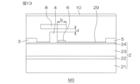
図13は、ゲート電極4がオーバーラップ部4aを有していない場合の実施形態のシミュレーションのモデルM3を示す模式図である。図13において、図3の各部に対応する部分には、図3と同じ符号を付して示す。図13において、bは、平面視において、ゲート電極4の電極部81の上面の+Y方向側縁からの、第2ソースフィールドプレート8の+Y方向側縁の突出量を示している。ゲート電極4の電極部81の上面の-Y方向側縁からの、第2ソースフィールドプレート8の-Y方向側縁の突出量は、ゲート電極4の+Y方向側縁からの、第2ソースフィールドプレート8の+Y方向側縁の突出量bと同じである。
Figure 13 is a schematic diagram showing a model M3 of a simulation of an embodiment in which the
図13に示す突出量bを、0μm、0.3μm、0.6μmおよび0.9μmに設定した場合のそれぞれについて、入力容量Ciss、出力容量Cossおよび帰還容量Crssを計算した。また、図13のモデルM3から、第2ソースフィールドプレート8を除去した構成を比較例のモデルとして、入力容量Ciss、出力容量Cossおよび帰還容量Crssをシミュレーションによって計算した。
The input capacitance Ciss, output capacitance Coss, and feedback capacitance Crss were calculated for each of the cases where the protrusion amount b shown in FIG. 13 was set to 0 μm, 0.3 μm, 0.6 μm, and 0.9 μm. In addition, the input capacitance Ciss, output capacitance Coss, and feedback capacitance Crss were calculated by simulation using a configuration in which the second
図14は、シミュレーション結果を示す表である。各容量Ciss、CossおよびCrssは、ドレイン・ソース間電圧Vdsが50Vのときの容量(pF)である。 Figure 14 is a table showing the simulation results. Each capacitance Ciss, Coss, and Crss is the capacitance (pF) when the drain-source voltage Vds is 50 V.
図14から、第2ソースフィールドプレート8を有する実施形態の方が、第2ソースフィールドプレート8を有していない比較例に比べて、帰還容量Crssが小さくなっていることがわかる。また、第2ソースフィールドプレート8を有している実施形態では、突出量bが大きいほど、帰還容量Crssが小さくなっていることがわかる。しかしながら、突出量bが大きくなるほど、第2ソースフィールドプレート8とソース電極3に接続されるソースビアメタル51(図4参照)との間の距離が短くなる。そこで、第2ソースフィールドプレート8がソースビアメタル51に近づきすぎない範囲で、突出量bを大きくすることが好ましい。このような観点から、突出量bは0.4μm以上0.8μm以下が好ましく、0.6μm程度がより好ましい。
From FIG. 14, it can be seen that the feedback capacitance Crss is smaller in the embodiment having the second
次に、ゲート電極4はオーバーラップ部4aを有していない場合において、突出量bを0.6μmに設定し、ゲート電極4の上面と第2ソースフィールドプレート8の下面との間隔d(図13参照)と、入力容量Ciss、出力容量Cossおよび帰還容量Crssとの関係をシミュレーションによって調べた。シミュレーションモデルは、図13と同様である。
Next, in the case where the
図15は、シミュレーション結果を示す表である。各容量Ciss、CossおよびCrssは、ドレイン・ソース間電圧Vdsが50Vのときの容量(pF)である。図15から、ゲート電極4と第2ソースフィールドプレート8との間隔dが小さいほど、帰還容量Crssが小さくなっていることがわかる。しかしながら、間隔dが小さくなるほど、入力容量Cissが大きくなる。そこで、入力容量Cissが大きくなりすぎない範囲で、間隔dを小さくすることが好ましい。このような観点から、間隔dは0.15μm以上0.25μm未満が好ましく、0.2μm程度がより好ましい。
Figure 15 is a table showing the simulation results. Each capacitance Ciss, Coss, and Crss is a capacitance (pF) when the drain-source voltage Vds is 50 V. From Figure 15, it can be seen that the smaller the distance d between the
前述の実施形態では、電極メタル構造におけるゲート電極4の電極部81と配線メタル構造におけるドレイン配線10とが直交して配置される半導体装置1において、ゲート電極4の電極部81とドレイン配線10との間に、ソース電極3に電気的に接続された第2ソースフィードプレート(導電膜)8が配置されている。これにより、ゲート電極4の電極部81とドレイン配線10との間の静電容量(第2のゲート・ドレイン間容量CGD2)が低減されるから、半導体装置1の帰還容量Crssを低減することができる。これにより、半導体装置1のスイッチング特性を向上させることができる。
In the above-described embodiment, in the
また、前述の実施形態では、電極メタル構造におけるソース電極3、ゲート電極4の電極部81およびドレイン電極5と、配線メタル構造におけるソース配線9、ドレイン配線10およびゲート配線11とが直交して配置されているので、ソース配線9およびドレイン配線10の幅が、ソース電極3とドレイン電極5との間隔によって制限されない。オン抵抗の小さいHEMTを実現するためには、ソース電極3とドレイン電極5との間隔を短くする必要があるが、この場合でも、ソース配線9およびドレイン配線10の幅を十分な大きさに設定しやすい。また、前述の実施形態では、ソース配線9、ドレイン配線10およびゲート配線11を同じ工程で形成することができるので、これらの配線の製造が簡単となる。
In addition, in the above-mentioned embodiment, the
電極メタル構造におけるソース電極3、ゲート電極4の電極部81およびドレイン電極5が延びる方向と、配線メタル構造におけるソース配線9、ドレイン配線10およびゲート配線11が延びる方向とを同じ方向にすると、ゲート電極4の電極部81の表面の全ての位置の真上にドレイン配線10が配置されないようにすることが可能となる。そうすると、ゲート電極4の電極部81とドレイン配線10とそれらの間の絶縁膜34,35とによって形成される静電容量(第2のゲート・ドレイン間容量CGD2)は小さくなる。したがって、そのような構造では、ゲート電極4の電極部81の上側に、第2のゲート・ドレイン間容量CGD2を低減させるための第2ソースフィールドプレート8のような導電膜を設ける必要はないかもしれない。しかしながら、電極メタル構造における電極3,4,5の延びる方向と、配線メタル構造における配線9,10,11の延びる方向を同じ方向にする場合には、次のような問題が発生するおそれがある。
If the direction in which the
すなわち、例えば、ソース電極上にソース配線を配置し、ドレイン電極上にドレイン配線を配置する場合、これらの配線の幅がソース電極とドレイン電極との間隔によって制限される。特に、オン抵抗の小さいHEMTを実現するためには、ソース電極とドレイン電極との間隔を短くする必要があるため、ソース配線およびドレイン配線の幅を十分にとることができなくなるおそれがある。 That is, for example, when a source wiring is arranged on a source electrode and a drain wiring is arranged on a drain electrode, the width of these wirings is limited by the distance between the source electrode and the drain electrode. In particular, in order to realize a HEMT with a low on-resistance, it is necessary to shorten the distance between the source electrode and the drain electrode, so there is a risk that the source wiring and the drain wiring will not be able to be made sufficiently wide.
また、ソース配線とドレイン配線との間の間隔を大きくすることは困難であるため、これらの間にゲート配線を形成することが困難となる。そのため、ソース配線およびドレイン配線と同じ工程によって、ゲート配線を形成することが困難となる。また、平面視において、ソース配線およびドレイン配線が存在しない領域まで、ゲート電極を延長する必要があるため、ゲート抵抗が大きくなるおそれがある。 In addition, since it is difficult to increase the distance between the source wiring and the drain wiring, it is difficult to form the gate wiring between them. This makes it difficult to form the gate wiring in the same process as the source wiring and the drain wiring. In addition, since it is necessary to extend the gate electrode to an area where there are no source wiring or drain wiring in a plan view, there is a risk of increasing the gate resistance.
前述の実施形態では、基板21の材料例としてシリコンを例示したが、ほかにも、サファイア基板やGaN基板などの任意の基板材料を適用できる。
In the above embodiment, silicon was used as an example of the material for the
本発明の実施形態について詳細に説明してきたが、これらは本発明の技術的内容を明らかにするために用いられた具体例に過ぎず、本発明はこれらの具体例に限定して解釈されるべきではなく、本発明の範囲は添付の請求の範囲によってのみ限定される。 Although the embodiments of the present invention have been described in detail, these are merely examples used to clarify the technical content of the present invention, and the present invention should not be interpreted as being limited to these examples, and the scope of the present invention is limited only by the scope of the attached claims.
この出願は、2018年1月19日に日本国特許庁に提出された特願2018-007397号に対応しており、その出願の全開示はここに引用により組み込まれるものとする。 This application corresponds to Patent Application No. 2018-007397 filed with the Japan Patent Office on January 19, 2018, the entire disclosure of which is incorporated herein by reference.
この明細書からはさらに以下のような特徴が抽出され得る。 Further features that can be extracted from this specification include:
A1.半導体積層構造上に配置され、互いに平行にかつ所定の第1方向に延びるソース電極、ゲート電極およびドレイン電極を含む電極構造と、電極構造上に配置され、互いに平行にかつ前記第1方向に直交する第2方向に延びるソース配線、ドレイン配線およびゲート配線を含む配線構造とを有し、前記ソース配線、ドレイン配線およびゲート配線が、それぞれ前記ソース電極、ドレイン電極およびゲート電極に電気的に接続されている半導体装置であって、前記ゲート電極と前記ドレイン配線との間に配置され、前記ソース電極に電気的に接続された導電膜を含む、半導体装置。 A1. A semiconductor device having an electrode structure arranged on a semiconductor laminate structure, the electrode structure including a source electrode, a gate electrode, and a drain electrode that are parallel to each other and extend in a predetermined first direction, and a wiring structure arranged on the electrode structure, the source wiring, the drain wiring, and the gate wiring that are parallel to each other and extend in a second direction perpendicular to the first direction, the source wiring, the drain wiring, and the gate wiring being electrically connected to the source electrode, the drain electrode, and the gate electrode, respectively, and the semiconductor device including a conductive film arranged between the gate electrode and the drain wiring and electrically connected to the source electrode.
この構成では、ゲート電極とドレイン配線との間の電気力線の少なくとも一部が導電膜によって遮断されるので、ゲート電極とドレイン配線とによって形成される静電容量を低減することができる、これにより、帰還容量を低減させることができるので、スイッチング特性を向上できる。 In this configuration, at least a portion of the electric field lines between the gate electrode and the drain wiring are blocked by the conductive film, so the capacitance formed by the gate electrode and the drain wiring can be reduced, thereby reducing the feedback capacitance and improving the switching characteristics.
A2.前記導電膜は、前記ゲート電極の上面に沿って前記第1方向に延びている、A1に記載の半導体装置。 A2. The semiconductor device according to A1, wherein the conductive film extends in the first direction along the upper surface of the gate electrode.
A3.前記導電膜の幅が前記ゲート電極の上面の幅よりも大きく、平面視において、前記導電膜の各側縁が、前記ゲート電極の上面の対応する側縁よりも外方に突出している、A2に記載の半導体装置。 A3. The semiconductor device according to A2, in which the width of the conductive film is greater than the width of the upper surface of the gate electrode, and in a plan view, each side edge of the conductive film protrudes outward beyond the corresponding side edge of the upper surface of the gate electrode.
A4.前記導電膜の各側縁の前記ゲート電極の上面の対応する側縁からの突出量が、0.3μm以上0.9μm以下である、A3に記載の半導体装置。 A4. The semiconductor device according to A3, in which the amount of protrusion of each side edge of the conductive film from the corresponding side edge of the upper surface of the gate electrode is 0.3 μm or more and 0.9 μm or less.
A5.前記ゲート電極の上面と前記導電膜の下面との間の距離が、0.15μm以上0.25μm以下である、A4に記載の半導体装置。 A5. The semiconductor device according to A4, in which the distance between the upper surface of the gate electrode and the lower surface of the conductive film is 0.15 μm or more and 0.25 μm or less.
A6.前記ソース電極および前記ドレイン電極は、前記ゲート電極を挟むように、前記ゲート電極から離れて配置されている、A1~A5のいずれかに記載の半導体装置。 A6. A semiconductor device according to any one of A1 to A5, in which the source electrode and the drain electrode are arranged apart from the gate electrode so as to sandwich the gate electrode.
A7.前記半導体積層構造は、前記ソース電極および前記ドレイン電極で前記ゲート電極を挟むことによって構成された素子構造を含むアクティブエリアと、前記アクティブエリア外のノンアクティブエリアとを含み、前記ノンアクティブエリアにおいて、前記ソース配線と前記導電膜とが電気的に接続されている、A6に記載の半導体装置。 A7. The semiconductor device according to A6, wherein the semiconductor laminate structure includes an active area including an element structure formed by sandwiching the gate electrode between the source electrode and the drain electrode, and a non-active area outside the active area, and the source wiring and the conductive film are electrically connected in the non-active area.
A8.前記半導体積層構造は、電子走行層と、前記電子走行層上に形成され、電子走行層に達する下側開口部が形成された電子供給層とを含み、前記半導体積層構造上には、前記下側開口部に連通する上側開口部を有する絶縁層が形成されており、前記絶縁層の表面および前記下側開口部および前記上側開口部からなるゲート開口部の底部および側部を覆うように、ゲート絶縁膜が形成されており、前記ゲート電極は、前記ゲート開口部内で前記ゲート絶縁膜上に形成されている、A6に記載の半導体装置。 A8. The semiconductor device according to A6, in which the semiconductor laminate structure includes an electron transit layer and an electron supply layer formed on the electron transit layer and having a lower opening reaching the electron transit layer, an insulating layer having an upper opening communicating with the lower opening is formed on the semiconductor laminate structure, a gate insulating film is formed so as to cover the surface of the insulating layer and the bottom and sides of a gate opening consisting of the lower opening and the upper opening, and the gate electrode is formed on the gate insulating film within the gate opening.
A9.前記ゲート電極と前記ドレイン電極との間で前記絶縁層に埋め込まれ、前記ゲート電極から絶縁され、前記ソース電極に電気的に接続された第2導電膜をさらに含む、A8に記載の半導体装置。 A9. The semiconductor device according to A8, further comprising a second conductive film embedded in the insulating layer between the gate electrode and the drain electrode, insulated from the gate electrode, and electrically connected to the source electrode.
A10.前記ゲート電極と前記ソース電極との間で前記絶縁層に埋め込まれ、前記ゲート電極および前記ソース電極から絶縁されている第3導電膜をさらに含む、A9に記載の半導体装置。 A10. The semiconductor device according to A9, further comprising a third conductive film embedded in the insulating layer between the gate electrode and the source electrode and insulated from the gate electrode and the source electrode.
A11.前記ゲート絶縁膜と前記ゲート開口部の側部との間に配置された絶縁性のサイドウォールをさらに含む、A9またはA10に記載の半導体装置。 A11. The semiconductor device according to A9 or A10, further comprising an insulating sidewall disposed between the gate insulating film and a side of the gate opening.
A12.前記ゲート電極は、前記ゲート開口部の周縁において、前記ゲート絶縁膜上に形成されたオーバーラップ部を含む、A8~A11のいずれかに記載の半導体装置。 A12. A semiconductor device according to any one of A8 to A11, in which the gate electrode includes an overlap portion formed on the gate insulating film at the periphery of the gate opening.
A13.電子走行層と前記電子走行層上に形成された電子供給層とを含む半導体積層構造上に、互いに平行にかつ所定の第1方向に延びたソース電極、ドレイン電極およびゲート電極を形成する工程と、前記ソース電極および前記ドレイン電極の上方に配置され、前記ゲート電極を覆う第1絶縁層を形成する工程と、前記第1絶縁層上の前記ゲート電極の上面に対向する位置に、導電膜を形成する工程と、前記第1絶縁層上に、前記導電膜を覆うように、第2絶縁層を形成する工程と、前記ソース電極、前記ドレイン電極および前記ゲート電極を、それぞれ、前記第2絶縁層上に形成されるソース配線、ドレイン配線およびゲート配線に接続するためのソースビアメタル、ドレインビアメタルおよびゲートビアメタルをそれらの間の絶縁層内に形成するとともに、前記導電膜を前記ソース配線に接続するための導電膜ビアメタルを前記第2絶縁層内に形成する工程と、前記第2絶縁層上に、互いに平行にかつ前記第2絶縁層の表面に沿う方向であって前記第1方向と直交する第2方向に延びた前記ソース配線、前記ドレイン配線および前記ゲート配線を形成する工程とを含む、半導体装置の製造方法。 A13. A method for manufacturing a semiconductor device, comprising the steps of forming a source electrode, a drain electrode, and a gate electrode that are parallel to each other and extend in a predetermined first direction on a semiconductor laminate structure including an electron transport layer and an electron supply layer formed on the electron transport layer, forming a first insulating layer that is disposed above the source electrode and the drain electrode and covers the gate electrode, forming a conductive film on the first insulating layer at a position facing the upper surface of the gate electrode, forming a second insulating layer on the first insulating layer so as to cover the conductive film, forming a source via metal, a drain via metal, and a gate via metal in the insulating layer between the source electrode, the drain electrode, and the gate electrode to the source wiring, the drain wiring, and the gate wiring formed on the second insulating layer, respectively, and forming a conductive film via metal in the second insulating layer to connect the conductive film to the source wiring, and forming the source wiring, the drain wiring, and the gate wiring on the second insulating layer in a second direction that is parallel to each other and extends along the surface of the second insulating layer and perpendicular to the first direction.
A14.前記導電膜は、前記ゲート電極の上面に沿って前記第1方向に延びている、A13に記載の半導体装置の製造方法。 A14. The method for manufacturing a semiconductor device according to A13, wherein the conductive film extends in the first direction along the upper surface of the gate electrode.
A15.前記導電膜の幅が前記ゲート電極の上面の幅よりも大きく、前記導電膜の各側縁が、前記ゲート電極の上面の対応する側縁よりも外方に突出している、A14に記載の半導体装置の製造方法。 A15. The method for manufacturing a semiconductor device according to A14, wherein the width of the conductive film is greater than the width of the upper surface of the gate electrode, and each side edge of the conductive film protrudes outward beyond the corresponding side edge of the upper surface of the gate electrode.
1 半導体装置
2 半導体積層構造
3 ソース電極
4 ゲート電極
4a オーバーラップ部
5 ドレイン電極
6 第1ソースフィールドプレート
7 フローティングプレート
8 第2ソースフィールドプレート
9 ソース配線
10 ドレイン配線
11 ゲート配線
12 ドレインパッド
13 ソースパッド
14 ゲートパッド
15 基板コンタクト部
16 アクティブエリア
17 ノンアクティブエリア
18 素子分離線
20 プレート膜
21 基板
22 バッファ層
23 電子走行層
24 電子供給層
25 二次元電子ガス
29 パッシベーション膜
31 第1保護膜
32 第2保護膜
33 第1層間絶縁膜
34 第2層間絶縁膜
35 第3層間絶縁膜
36 ソースコンタクトホール
37 ドレインコンタクトホール
38 ゲート開口部
38a 第1開口部
38b 第2開口部
39 サイドウォール
40 ゲート絶縁膜
41 第1ソースビアホール
42 第1ドレインビアホール
43 第1ゲートビアホール
44 第1SFP用ビアホール
45 第2SFP用ビアホール
51 ソースビアメタル
52 ドレインビアメタル
53 ゲートビアメタル
54 第1SFP用ビアメタル
55 第2SFP用ビアメタル
61 第4層間絶縁膜
62 第2ドレインビアホール
63 基板コンタクトホール
64 基板コンタクトメタル
65 第3保護膜
66 ドレインパッド開口部
67 樹脂層
72 ベース部
73 電極部(第1ソースフィールドプレート6)
74 ベース部
75 電極部(フローティングプレート7)
76 ベース部
81 電極部(ゲート電極4)
82 ベース部
91 電極部(第2ソースフィールドプレート8)
92 ベース部
LIST OF
74
76
82
92 Base part
Claims (16)
第1導電膜と、前記ソース電極と電気的に接続された第2導電膜と、前記ソース電極と電気的に接続された第3導電膜とを含み、
ある断面において、
前記第1導電膜は、前記ソース電極と前記ゲート電極の間に配置され、
前記第2導電膜は、前記ゲート電極と前記ドレイン電極との間に配置され、かつその最上面が前記ゲート電極の最上面よりも前記半導体積層構造に対して近接して配置されており、
前記第3導電膜は、前記ゲート電極の上方であって前記ドレイン配線の下方に配置されており、
前記第1導電膜は、前記半導体積層構造の表面と水平な方向に延出する部分を有し、
前記第2導電膜は、前記半導体積層構造の表面と水平な方向に延出する部分を有し、
前記第3導電膜は、前記半導体積層構造の表面と水平な方向に延出する部分を有し、
前記第1導電膜は、前記第2導電膜と同一のレイヤーに形成されており、
前記ソース配線は、前記ソース電極とは材料が異なるソースビアメタルを介して、前記ソース電極に接続され、
前記ドレイン配線は、前記ドレイン電極とは材料が異なるドレインビアメタルを介して、前記ドレイン電極に接続され、
前記ゲート配線は、前記ゲート電極とは材料が異なるゲートビアメタルを介して、前記ゲート電極に接続されており、
前記ソース電極および前記ドレイン電極は、Ti膜、AlSiCu膜、Ti膜およびTiN膜が、下層からその順に積層されたTi/AlSiCu/Ti/TiN積層膜から構成されている、半導体装置。 A semiconductor device having a source electrode, a gate electrode and a drain electrode arranged on a semiconductor laminate structure, a source wiring electrically connected to the source electrode, a drain wiring electrically connected to the drain electrode, and a gate wiring electrically connected to the gate electrode,
a first conductive film, a second conductive film electrically connected to the source electrode, and a third conductive film electrically connected to the source electrode;
In a certain cross section,
the first conductive film is disposed between the source electrode and the gate electrode;
the second conductive film is disposed between the gate electrode and the drain electrode, and a top surface of the second conductive film is disposed closer to the semiconductor laminated structure than a top surface of the gate electrode;
the third conductive film is disposed above the gate electrode and below the drain wiring ,
the first conductive film has a portion extending in a direction parallel to a surface of the semiconductor laminated structure,
the second conductive film has a portion extending in a direction parallel to a surface of the semiconductor laminated structure,
the third conductive film has a portion extending in a direction parallel to a surface of the semiconductor laminated structure,
the first conductive film is formed in the same layer as the second conductive film,
the source wiring is connected to the source electrode via a source via metal made of a material different from that of the source electrode;
the drain wiring is connected to the drain electrode via a drain via metal made of a material different from that of the drain electrode;
the gate wiring is connected to the gate electrode via a gate via metal made of a material different from that of the gate electrode;
the source electrode and the drain electrode are formed of a Ti/AlSiCu/Ti/TiN laminated film in which a Ti film, an AlSiCu film, a Ti film and a TiN film are laminated in this order from the bottom up.
前記第3導電膜は、前記ゲート電極の上面に沿って前記第1方向に延びている、請求項3に記載の半導体装置。 the source electrode, the gate electrode, and the drain electrode extend in a predetermined first direction,
The semiconductor device according to claim 3 , wherein said third conductive film extends in said first direction along an upper surface of said gate electrode.
前記ノンアクティブエリアにおいて、前記ソース配線と前記第3導電膜とが電気的に接続されている、請求項8に記載の半導体装置。 the semiconductor laminated structure includes an active area including an element structure formed by sandwiching the gate electrode between the source electrode and the drain electrode, and a non-active area outside the active area;
9. The semiconductor device according to claim 8 , wherein the source wiring and the third conductive film are electrically connected in the non-active area.
前記半導体積層構造上には、前記下側開口部に連通する上側開口部を有する絶縁層が形成されており、
前記絶縁層の表面および前記下側開口部および前記上側開口部からなるゲート開口部の底部および側部を覆うように、ゲート絶縁膜が形成されており、
前記ゲート電極は、前記ゲート開口部内で前記ゲート絶縁膜上に形成されている、請求項9に記載の半導体装置。 the semiconductor laminated structure includes an electron transit layer, and an electron supply layer formed on the electron transit layer and having a lower opening reaching the electron transit layer;
an insulating layer having an upper opening communicating with the lower opening is formed on the semiconductor laminate structure;
a gate insulating film is formed so as to cover a surface of the insulating layer and a bottom and side of a gate opening formed by the lower opening and the upper opening;
10. The semiconductor device according to claim 9 , wherein said gate electrode is formed on said gate insulating film within said gate opening.
前記第2導電膜は、前記ゲート開口部の一側部の高さ中間位置で露出している、請求項10に記載の半導体装置。 the second conductive film is embedded in the insulating layer between the gate electrode and the drain electrode, insulated from the gate electrode, and electrically connected to the source electrode;
The semiconductor device according to claim 10 , wherein the second conductive film is exposed at a middle position in height of one side of the gate opening.
前記ソースビアメタル、前記ドレインビアメタルおよび前記ゲートビアメタルは、対応するビアホールの側壁に形成されるTiNバリア膜と、前記TiNバリア膜の内側に埋め込まれるタングステンとから構成される、請求項14に記載の半導体装置。 the source via metal, the drain via metal, and the gate via metal are buried in a source via hole, a drain via hole, and a gate via hole, respectively;
15. The semiconductor device according to claim 14 , wherein the source via metal, the drain via metal and the gate via metal are each composed of a TiN barrier film formed on a side wall of a corresponding via hole and tungsten embedded inside the TiN barrier film.
Applications Claiming Priority (4)
| Application Number | Priority Date | Filing Date | Title |
|---|---|---|---|
| JP2018007397 | 2018-01-19 | ||
| JP2018007397 | 2018-01-19 | ||
| JP2019565755A JP7208167B2 (en) | 2018-01-19 | 2018-12-05 | Semiconductor device and its manufacturing method |
| PCT/JP2018/044754 WO2019142529A1 (en) | 2018-01-19 | 2018-12-05 | Semiconductor device and method for producing same |
Related Parent Applications (1)
| Application Number | Title | Priority Date | Filing Date |
|---|---|---|---|
| JP2019565755A Division JP7208167B2 (en) | 2018-01-19 | 2018-12-05 | Semiconductor device and its manufacturing method |
Publications (2)
| Publication Number | Publication Date |
|---|---|
| JP2023040154A JP2023040154A (en) | 2023-03-22 |
| JP7547518B2 true JP7547518B2 (en) | 2024-09-09 |
Family
ID=67302147
Family Applications (2)
| Application Number | Title | Priority Date | Filing Date |
|---|---|---|---|
| JP2019565755A Active JP7208167B2 (en) | 2018-01-19 | 2018-12-05 | Semiconductor device and its manufacturing method |
| JP2023000656A Active JP7547518B2 (en) | 2018-01-19 | 2023-01-05 | Semiconductor Device |
Family Applications Before (1)
| Application Number | Title | Priority Date | Filing Date |
|---|---|---|---|
| JP2019565755A Active JP7208167B2 (en) | 2018-01-19 | 2018-12-05 | Semiconductor device and its manufacturing method |
Country Status (3)
| Country | Link |
|---|---|
| US (3) | US11694954B2 (en) |
| JP (2) | JP7208167B2 (en) |
| WO (1) | WO2019142529A1 (en) |
Families Citing this family (8)
| Publication number | Priority date | Publication date | Assignee | Title |
|---|---|---|---|---|
| JP7177660B2 (en) * | 2018-10-26 | 2022-11-24 | 株式会社東芝 | semiconductor equipment |
| JP7366576B2 (en) * | 2019-04-15 | 2023-10-23 | 株式会社東芝 | semiconductor equipment |
| JP7368107B2 (en) * | 2019-05-22 | 2023-10-24 | 株式会社東芝 | semiconductor equipment |
| CN114664725B (en) * | 2020-12-23 | 2025-07-29 | 华润微电子(重庆)有限公司 | GaN device interconnection structure and preparation method thereof |
| JP7705048B2 (en) * | 2022-03-15 | 2025-07-09 | 富士通株式会社 | Semiconductor device, manufacturing method thereof, and electronic device |
| US20240128328A1 (en) * | 2022-10-12 | 2024-04-18 | Globalfoundries U.S. Inc. | Device with field plates |
| US20240194680A1 (en) * | 2022-12-09 | 2024-06-13 | Globalfoundries U.S. Inc. | Bidirectional device |
| CN117457735A (en) * | 2023-12-22 | 2024-01-26 | 英诺赛科(珠海)科技有限公司 | Transistor structure and manufacturing method and chip |
Citations (8)
| Publication number | Priority date | Publication date | Assignee | Title |
|---|---|---|---|---|
| WO2010047016A1 (en) | 2008-10-21 | 2010-04-29 | パナソニック株式会社 | Bidirectional switch |
| JP2010118556A (en) | 2008-11-13 | 2010-05-27 | Furukawa Electric Co Ltd:The | Semiconductor device and its manufacturing method |
| US20100259321A1 (en) | 2009-04-14 | 2010-10-14 | Triquint Semiconductor, Inc. | Field effect transistor having a plurality of field plates |
| JP2012178595A (en) | 2005-03-11 | 2012-09-13 | Cree Inc | Wide bandgap transistors with gate-source field plates |
| JP2013131758A (en) | 2011-12-21 | 2013-07-04 | Power Integrations Inc | Semiconductor devices |
| WO2014073295A1 (en) | 2012-11-09 | 2014-05-15 | シャープ株式会社 | Field-effect transistor |
| WO2014188651A1 (en) | 2013-05-20 | 2014-11-27 | パナソニックIpマネジメント株式会社 | Semiconductor device |
| JP2016134599A (en) | 2015-01-22 | 2016-07-25 | ローム株式会社 | Semiconductor device and semiconductor device manufacturing method |
Family Cites Families (14)
| Publication number | Priority date | Publication date | Assignee | Title |
|---|---|---|---|---|
| JP5735099B2 (en) | 2011-04-01 | 2015-06-17 | ルネサスエレクトロニクス株式会社 | Semiconductor device, method of manufacturing the same, and mobile phone |
| JP5827529B2 (en) | 2011-09-15 | 2015-12-02 | ローム株式会社 | Nitride semiconductor device and manufacturing method thereof |
| JP2014072379A (en) * | 2012-09-28 | 2014-04-21 | Fujitsu Ltd | Compound semiconductor device and manufacturing method of the same |
| TWI566328B (en) * | 2013-07-29 | 2017-01-11 | 高效電源轉換公司 | Gallium nitride transistor having a polysilicon layer for generating additional components |
| US10236236B2 (en) * | 2013-09-10 | 2019-03-19 | Delta Electronics, Inc. | Heterojunction semiconductor device for reducing parasitic capacitance |
| JP6332021B2 (en) * | 2014-12-26 | 2018-05-30 | 株式会社デンソー | Semiconductor device |
| TWI626742B (en) * | 2015-06-18 | 2018-06-11 | 台達電子工業股份有限公司 | Semiconductor device |
| JP6642883B2 (en) * | 2015-10-08 | 2020-02-12 | ローム株式会社 | Nitride semiconductor device and method of manufacturing the same |
| US9741840B1 (en) * | 2016-06-14 | 2017-08-22 | Semiconductor Components Industries, Llc | Electronic device including a multiple channel HEMT and an insulated gate electrode |
| US9673311B1 (en) * | 2016-06-14 | 2017-06-06 | Semiconductor Components Industries, Llc | Electronic device including a multiple channel HEMT |
| US10263085B2 (en) * | 2016-12-30 | 2019-04-16 | Texas Instruments Incorporated | Transistor with source field plates and non-overlapping gate runner layers |
| US10461161B1 (en) * | 2017-01-23 | 2019-10-29 | Navitas Semiconductor, Inc. | GaN device with floating field plates |
| JP7316757B2 (en) * | 2018-02-23 | 2023-07-28 | ローム株式会社 | semiconductor equipment |
| TWI811394B (en) * | 2019-07-09 | 2023-08-11 | 聯華電子股份有限公司 | High electron mobility transistor and method for fabricating the same |
-
2018
- 2018-12-05 WO PCT/JP2018/044754 patent/WO2019142529A1/en not_active Ceased
- 2018-12-05 JP JP2019565755A patent/JP7208167B2/en active Active
- 2018-12-05 US US16/962,762 patent/US11694954B2/en active Active
-
2023
- 2023-01-05 JP JP2023000656A patent/JP7547518B2/en active Active
- 2023-05-16 US US18/318,423 patent/US12199028B2/en active Active
-
2024
- 2024-12-04 US US18/967,990 patent/US20250096110A1/en active Pending
Patent Citations (8)
| Publication number | Priority date | Publication date | Assignee | Title |
|---|---|---|---|---|
| JP2012178595A (en) | 2005-03-11 | 2012-09-13 | Cree Inc | Wide bandgap transistors with gate-source field plates |
| WO2010047016A1 (en) | 2008-10-21 | 2010-04-29 | パナソニック株式会社 | Bidirectional switch |
| JP2010118556A (en) | 2008-11-13 | 2010-05-27 | Furukawa Electric Co Ltd:The | Semiconductor device and its manufacturing method |
| US20100259321A1 (en) | 2009-04-14 | 2010-10-14 | Triquint Semiconductor, Inc. | Field effect transistor having a plurality of field plates |
| JP2013131758A (en) | 2011-12-21 | 2013-07-04 | Power Integrations Inc | Semiconductor devices |
| WO2014073295A1 (en) | 2012-11-09 | 2014-05-15 | シャープ株式会社 | Field-effect transistor |
| WO2014188651A1 (en) | 2013-05-20 | 2014-11-27 | パナソニックIpマネジメント株式会社 | Semiconductor device |
| JP2016134599A (en) | 2015-01-22 | 2016-07-25 | ローム株式会社 | Semiconductor device and semiconductor device manufacturing method |
Also Published As
| Publication number | Publication date |
|---|---|
| WO2019142529A1 (en) | 2019-07-25 |
| US20200357736A1 (en) | 2020-11-12 |
| JP7208167B2 (en) | 2023-01-18 |
| JP2023040154A (en) | 2023-03-22 |
| US12199028B2 (en) | 2025-01-14 |
| US20230326846A1 (en) | 2023-10-12 |
| JPWO2019142529A1 (en) | 2021-01-07 |
| US20250096110A1 (en) | 2025-03-20 |
| US11694954B2 (en) | 2023-07-04 |
Similar Documents
| Publication | Publication Date | Title |
|---|---|---|
| JP7547518B2 (en) | Semiconductor Device | |
| JP7539447B2 (en) | Semiconductor Device | |
| CN104009075B (en) | Semiconductor device | |
| JP5348364B2 (en) | Heterojunction field effect semiconductor device | |
| US20220285541A1 (en) | Nitride semiconductor device | |
| JP6496149B2 (en) | Semiconductor device and manufacturing method of semiconductor device | |
| JP7464763B2 (en) | Nitride Semiconductor Device | |
| CN101299437A (en) | field effect transistor | |
| CN107887448A (en) | Semiconductor devices | |
| JP2017073499A (en) | Nitride semiconductor device and method for manufacturing the same | |
| CN110785836A (en) | Semiconductor device with a plurality of semiconductor chips | |
| JP7161915B2 (en) | semiconductor equipment | |
| CN105453273A (en) | Integrated circuit with matching threshold voltages and method for making same | |
| TW202145345A (en) | Nitride semiconductor device | |
| JP2008034522A (en) | Field effect transistor | |
| JP5985162B2 (en) | Nitride semiconductor device | |
| CN103314438A (en) | Nitride semiconductor device | |
| JP2011192944A (en) | Semiconductor device and method of operating semiconductor device | |
| JP7512326B2 (en) | Semiconductor Device | |
| JP6689424B2 (en) | Semiconductor device | |
| JP2024116730A (en) | Nitride Semiconductor Device | |
| WO2023224092A1 (en) | Nitride semiconductor device | |
| JP2024012856A (en) | nitride semiconductor device |
Legal Events
| Date | Code | Title | Description |
|---|---|---|---|
| A621 | Written request for application examination |
Free format text: JAPANESE INTERMEDIATE CODE: A621 Effective date: 20230105 |
|
| A131 | Notification of reasons for refusal |
Free format text: JAPANESE INTERMEDIATE CODE: A131 Effective date: 20240328 |
|
| A521 | Request for written amendment filed |
Free format text: JAPANESE INTERMEDIATE CODE: A523 Effective date: 20240521 |
|
| TRDD | Decision of grant or rejection written | ||
| A01 | Written decision to grant a patent or to grant a registration (utility model) |
Free format text: JAPANESE INTERMEDIATE CODE: A01 Effective date: 20240822 |
|
| A61 | First payment of annual fees (during grant procedure) |
Free format text: JAPANESE INTERMEDIATE CODE: A61 Effective date: 20240828 |
|
| R150 | Certificate of patent or registration of utility model |
Ref document number: 7547518 Country of ref document: JP Free format text: JAPANESE INTERMEDIATE CODE: R150 |