JP6495130B2 - 半導体装置及びその製造方法 - Google Patents
半導体装置及びその製造方法 Download PDFInfo
- Publication number
- JP6495130B2 JP6495130B2 JP2015146891A JP2015146891A JP6495130B2 JP 6495130 B2 JP6495130 B2 JP 6495130B2 JP 2015146891 A JP2015146891 A JP 2015146891A JP 2015146891 A JP2015146891 A JP 2015146891A JP 6495130 B2 JP6495130 B2 JP 6495130B2
- Authority
- JP
- Japan
- Prior art keywords
- semiconductor chip
- pad
- electrode
- connection terminal
- layer
- Prior art date
- Legal status (The legal status is an assumption and is not a legal conclusion. Google has not performed a legal analysis and makes no representation as to the accuracy of the status listed.)
- Active
Links
Images


Classifications
-
- H—ELECTRICITY
- H01—ELECTRIC ELEMENTS
- H01L—SEMICONDUCTOR DEVICES NOT COVERED BY CLASS H10
- H01L25/00—Assemblies consisting of a plurality of individual semiconductor or other solid state devices ; Multistep manufacturing processes thereof
- H01L25/03—Assemblies consisting of a plurality of individual semiconductor or other solid state devices ; Multistep manufacturing processes thereof all the devices being of a type provided for in the same subgroup of groups H01L27/00 - H01L33/00, or in a single subclass of H10K, H10N, e.g. assemblies of rectifier diodes
- H01L25/04—Assemblies consisting of a plurality of individual semiconductor or other solid state devices ; Multistep manufacturing processes thereof all the devices being of a type provided for in the same subgroup of groups H01L27/00 - H01L33/00, or in a single subclass of H10K, H10N, e.g. assemblies of rectifier diodes the devices not having separate containers
- H01L25/065—Assemblies consisting of a plurality of individual semiconductor or other solid state devices ; Multistep manufacturing processes thereof all the devices being of a type provided for in the same subgroup of groups H01L27/00 - H01L33/00, or in a single subclass of H10K, H10N, e.g. assemblies of rectifier diodes the devices not having separate containers the devices being of a type provided for in group H01L27/00
- H01L25/0657—Stacked arrangements of devices
-
- H—ELECTRICITY
- H01—ELECTRIC ELEMENTS
- H01L—SEMICONDUCTOR DEVICES NOT COVERED BY CLASS H10
- H01L25/00—Assemblies consisting of a plurality of individual semiconductor or other solid state devices ; Multistep manufacturing processes thereof
- H01L25/50—Multistep manufacturing processes of assemblies consisting of devices, each device being of a type provided for in group H01L27/00 or H01L29/00
-
- H—ELECTRICITY
- H01—ELECTRIC ELEMENTS
- H01L—SEMICONDUCTOR DEVICES NOT COVERED BY CLASS H10
- H01L2224/00—Indexing scheme for arrangements for connecting or disconnecting semiconductor or solid-state bodies and methods related thereto as covered by H01L24/00
- H01L2224/01—Means for bonding being attached to, or being formed on, the surface to be connected, e.g. chip-to-package, die-attach, "first-level" interconnects; Manufacturing methods related thereto
- H01L2224/10—Bump connectors; Manufacturing methods related thereto
- H01L2224/15—Structure, shape, material or disposition of the bump connectors after the connecting process
- H01L2224/16—Structure, shape, material or disposition of the bump connectors after the connecting process of an individual bump connector
- H01L2224/161—Disposition
- H01L2224/16135—Disposition the bump connector connecting between different semiconductor or solid-state bodies, i.e. chip-to-chip
- H01L2224/16145—Disposition the bump connector connecting between different semiconductor or solid-state bodies, i.e. chip-to-chip the bodies being stacked
-
- H—ELECTRICITY
- H01—ELECTRIC ELEMENTS
- H01L—SEMICONDUCTOR DEVICES NOT COVERED BY CLASS H10
- H01L2224/00—Indexing scheme for arrangements for connecting or disconnecting semiconductor or solid-state bodies and methods related thereto as covered by H01L24/00
- H01L2224/73—Means for bonding being of different types provided for in two or more of groups H01L2224/10, H01L2224/18, H01L2224/26, H01L2224/34, H01L2224/42, H01L2224/50, H01L2224/63, H01L2224/71
- H01L2224/732—Location after the connecting process
- H01L2224/73201—Location after the connecting process on the same surface
- H01L2224/73203—Bump and layer connectors
- H01L2224/73204—Bump and layer connectors the bump connector being embedded into the layer connector
-
- H—ELECTRICITY
- H01—ELECTRIC ELEMENTS
- H01L—SEMICONDUCTOR DEVICES NOT COVERED BY CLASS H10
- H01L2225/00—Details relating to assemblies covered by the group H01L25/00 but not provided for in its subgroups
- H01L2225/03—All the devices being of a type provided for in the same subgroup of groups H01L27/00 - H01L33/648 and H10K99/00
- H01L2225/04—All the devices being of a type provided for in the same subgroup of groups H01L27/00 - H01L33/648 and H10K99/00 the devices not having separate containers
- H01L2225/065—All the devices being of a type provided for in the same subgroup of groups H01L27/00 - H01L33/648 and H10K99/00 the devices not having separate containers the devices being of a type provided for in group H01L27/00
- H01L2225/06503—Stacked arrangements of devices
- H01L2225/06513—Bump or bump-like direct electrical connections between devices, e.g. flip-chip connection, solder bumps
-
- H—ELECTRICITY
- H01—ELECTRIC ELEMENTS
- H01L—SEMICONDUCTOR DEVICES NOT COVERED BY CLASS H10
- H01L2225/00—Details relating to assemblies covered by the group H01L25/00 but not provided for in its subgroups
- H01L2225/03—All the devices being of a type provided for in the same subgroup of groups H01L27/00 - H01L33/648 and H10K99/00
- H01L2225/04—All the devices being of a type provided for in the same subgroup of groups H01L27/00 - H01L33/648 and H10K99/00 the devices not having separate containers
- H01L2225/065—All the devices being of a type provided for in the same subgroup of groups H01L27/00 - H01L33/648 and H10K99/00 the devices not having separate containers the devices being of a type provided for in group H01L27/00
- H01L2225/06503—Stacked arrangements of devices
- H01L2225/06517—Bump or bump-like direct electrical connections from device to substrate
-
- H—ELECTRICITY
- H01—ELECTRIC ELEMENTS
- H01L—SEMICONDUCTOR DEVICES NOT COVERED BY CLASS H10
- H01L2225/00—Details relating to assemblies covered by the group H01L25/00 but not provided for in its subgroups
- H01L2225/03—All the devices being of a type provided for in the same subgroup of groups H01L27/00 - H01L33/648 and H10K99/00
- H01L2225/04—All the devices being of a type provided for in the same subgroup of groups H01L27/00 - H01L33/648 and H10K99/00 the devices not having separate containers
- H01L2225/065—All the devices being of a type provided for in the same subgroup of groups H01L27/00 - H01L33/648 and H10K99/00 the devices not having separate containers the devices being of a type provided for in group H01L27/00
- H01L2225/06503—Stacked arrangements of devices
- H01L2225/06527—Special adaptation of electrical connections, e.g. rewiring, engineering changes, pressure contacts, layout
-
- H—ELECTRICITY
- H01—ELECTRIC ELEMENTS
- H01L—SEMICONDUCTOR DEVICES NOT COVERED BY CLASS H10
- H01L2225/00—Details relating to assemblies covered by the group H01L25/00 but not provided for in its subgroups
- H01L2225/03—All the devices being of a type provided for in the same subgroup of groups H01L27/00 - H01L33/648 and H10K99/00
- H01L2225/04—All the devices being of a type provided for in the same subgroup of groups H01L27/00 - H01L33/648 and H10K99/00 the devices not having separate containers
- H01L2225/065—All the devices being of a type provided for in the same subgroup of groups H01L27/00 - H01L33/648 and H10K99/00 the devices not having separate containers the devices being of a type provided for in group H01L27/00
- H01L2225/06503—Stacked arrangements of devices
- H01L2225/06541—Conductive via connections through the device, e.g. vertical interconnects, through silicon via [TSV]
-
- H—ELECTRICITY
- H01—ELECTRIC ELEMENTS
- H01L—SEMICONDUCTOR DEVICES NOT COVERED BY CLASS H10
- H01L2225/00—Details relating to assemblies covered by the group H01L25/00 but not provided for in its subgroups
- H01L2225/03—All the devices being of a type provided for in the same subgroup of groups H01L27/00 - H01L33/648 and H10K99/00
- H01L2225/04—All the devices being of a type provided for in the same subgroup of groups H01L27/00 - H01L33/648 and H10K99/00 the devices not having separate containers
- H01L2225/065—All the devices being of a type provided for in the same subgroup of groups H01L27/00 - H01L33/648 and H10K99/00 the devices not having separate containers the devices being of a type provided for in group H01L27/00
- H01L2225/06503—Stacked arrangements of devices
- H01L2225/06555—Geometry of the stack, e.g. form of the devices, geometry to facilitate stacking
- H01L2225/06562—Geometry of the stack, e.g. form of the devices, geometry to facilitate stacking at least one device in the stack being rotated or offset
-
- H—ELECTRICITY
- H01—ELECTRIC ELEMENTS
- H01L—SEMICONDUCTOR DEVICES NOT COVERED BY CLASS H10
- H01L23/00—Details of semiconductor or other solid state devices
- H01L23/28—Encapsulations, e.g. encapsulating layers, coatings, e.g. for protection
- H01L23/31—Encapsulations, e.g. encapsulating layers, coatings, e.g. for protection characterised by the arrangement or shape
- H01L23/3107—Encapsulations, e.g. encapsulating layers, coatings, e.g. for protection characterised by the arrangement or shape the device being completely enclosed
- H01L23/3121—Encapsulations, e.g. encapsulating layers, coatings, e.g. for protection characterised by the arrangement or shape the device being completely enclosed a substrate forming part of the encapsulation
- H01L23/3128—Encapsulations, e.g. encapsulating layers, coatings, e.g. for protection characterised by the arrangement or shape the device being completely enclosed a substrate forming part of the encapsulation the substrate having spherical bumps for external connection
-
- H—ELECTRICITY
- H01—ELECTRIC ELEMENTS
- H01L—SEMICONDUCTOR DEVICES NOT COVERED BY CLASS H10
- H01L2924/00—Indexing scheme for arrangements or methods for connecting or disconnecting semiconductor or solid-state bodies as covered by H01L24/00
- H01L2924/15—Details of package parts other than the semiconductor or other solid state devices to be connected
- H01L2924/151—Die mounting substrate
- H01L2924/153—Connection portion
- H01L2924/1531—Connection portion the connection portion being formed only on the surface of the substrate opposite to the die mounting surface
- H01L2924/15311—Connection portion the connection portion being formed only on the surface of the substrate opposite to the die mounting surface being a ball array, e.g. BGA
Description
[第1の実施の形態に係る半導体装置の構造]
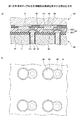
まず、第1の実施の形態に係る半導体装置の構造について説明する。図1は、第1の実施の形態に係る半導体装置を例示する断面図である。図2は、第1の実施の形態に係る半導体装置における半導体チップ同士の接続部の平面透視図である。
配線基板10は、コア層11の両面に配線層及び絶縁層が積層された配線基板である。具体的には、コア層11の一方の面には、配線層13、絶縁層14、配線層15、及びソルダーレジスト層16が順次積層されている。又、コア層11の他方の面には、配線層23、絶縁層24、配線層25、及びソルダーレジスト層26が順次積層されている。
半導体チップ30(第1の半導体チップ)は、配線基板10の一方の面にフェイスダウン状態で(回路形成面を配線基板10の一方の面に向けて)フリップチップ実装されている。半導体チップ30は、半導体基板31と、絶縁層32と、絶縁膜33と、貫通電極34と、パッド35と、配線層36と、ビア配線37と、パッド38と、絶縁層39と、保護膜40と、接続端子41とを備えている。
半導体チップ50(第2の半導体チップ)は、半導体基板51と、保護膜52と、パッド53と、接続端子54とを備えており、接続端子54が形成された側とパッド35が形成された側とが対向するように、半導体チップ30上に積層されている。言い換えれば、半導体チップ50は、半導体チップ30の一方の面(回路形成面とは反対側の面)にフェイスダウン状態でフリップチップ実装されている。
配線基板10と半導体チップ30との間には、接続端子41や接合部62を被覆するアンダーフィル樹脂71が充填されている。半導体チップ30と半導体チップ50との間には、接続端子54や接合部63を被覆するアンダーフィル樹脂72が充填されている。アンダーフィル樹脂72は、配線基板10と半導体チップ50との間のアンダーフィル樹脂71の周囲に延伸している。更に、配線基板10上には、半導体チップ30及び50やアンダーフィル樹脂71及び72を封止する封止樹脂79が設けられている。アンダーフィル樹脂71及び72、封止樹脂79の材料としては、例えば、エポキシ系樹脂等を用いることができる。
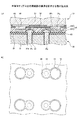
図3は、図1の半導体チップ同士の接続部の構造を例示する部分拡大図であり、図3(a)は断面図、図3(b)は平面透視図である。前述のように、半導体チップ30において、貫通電極34の上端面には、パッド35が形成されている。パッド35の平面形状は例えば円形であり、パッド35の外周側は貫通電極34の上端面から周囲(絶縁層32の上面)に延伸している。貫通電極34の直径は、例えば、5〜20μm程度である。パッド35の外周側は、例えば、数μm程度貫通電極34の上端面から絶縁層32の上面に円環状に延伸している。
次に、第1の実施の形態に係る半導体装置の製造方法について説明する。図5及び図6は、第1の実施の形態に係る半導体装置の製造工程を例示する図である。
第2の実施の形態では、半導体チップを更に多段に積層する例を示す。なお、第2の実施の形態において、既に説明した実施の形態と同一構成部についての説明は省略する場合がある。
第1の実施の形態の変形例では、貫通電極34と接続端子54とをずらす方向を統一しない例を示す。なお、第1の実施の形態の変形例において、既に説明した実施の形態と同一構成部についての説明は省略する場合がある。
10 配線基板
11 コア層
12 貫通配線
13、15、23、25、36 配線層
14、24、32、39 絶縁層
16、26 ソルダーレジスト層
16x、26x、40x、52x 開口部
30、50、80、90 半導体チップ
31、51 半導体基板
31x 貫通孔
33 絶縁膜
34 貫通電極
35、38、53 パッド
37 ビア配線
40、52 保護膜
41、54 接続端子
61 はんだバンプ
62、63 接合部
71、72、73、74 アンダーフィル樹脂
79 封止樹脂
351 内側めっき層
352 外側めっき層
Claims (14)
- 貫通電極、及び前記貫通電極の一端面に形成されたパッド、を備えた第1の半導体チップと、
接続端子を備え、前記接続端子が形成された側と前記パッドが形成された側とが対向するように、前記第1の半導体チップ上に積層された第2の半導体チップと、
前記第1の半導体チップと前記第2の半導体チップの間に設けられた導電性の接合部と、を有し、
前記第1の半導体チップと前記第2の半導体チップとは、前記貫通電極の前記一端面と、前記接続端子の前記第1の半導体チップと対向する面とが、平面視で重複しないように配されており、
前記導電性の接合部は前記パッドと前記接続端子を電気的に接続し、前記パッド上の第1の部分と、前記第1の半導体チップの前記第2の半導体チップに対向する面上にあり、前記第1の部分から延伸する第2の部分と、を有し、
前記接続端子は前記第2の部分と直接接触している半導体装置。 - 前記パッドは、中央部が高く外周側に行くにつれて高さが低くなる凸形状のドーム型である請求項1に記載の半導体装置。
- 前記パッドは、前記貫通電極の前記一端面から周囲に延伸している請求項1又は2に記載の半導体装置。
- 前記導電性の接合部は、前記接続端子の前記第1の半導体チップと対向する面に形成され、前記パッドの表面を覆っている請求項1乃至3の何れか一項に記載の半導体装置。
- 平面視で、前記導電性の接合部は前記第1の部分と前記第2の部分の連結部で狭まっている請求項4に記載の半導体装置。
- 前記貫通電極は、互いに隣接する第1の貫通電極及び第2の貫通電極を含み、
前記接続端子は、互いに隣接する第1の接続端子及び第2の接続端子を含み、
前記第1の貫通電極の前記第2の半導体チップと対向する面と、前記第1の接続端子の前記第1の半導体チップと対向する面とは、平面視で重複しないように所定の方向にずれて配されており、
前記第2の貫通電極の前記第2の半導体チップと対向する面と、前記第2の接続端子の前記第1の半導体チップと対向する面とは、平面視で重複しないように前記所定の方向とは異なる方向にずれて配されている請求項1乃至5の何れか一項に記載の半導体装置。 - 前記パッドは、前記貫通電極の前記一端面と接する内側めっき層と、前記内側めっき層の表面全体を被覆する外側めっき層とを含む請求項1乃至6の何れか一項に記載の半導体装置。
- 前記外側めっき層は金層である請求項7に記載の半導体装置。
- 前記第1の半導体チップが積層方向に積層されている、少なくとも一つの第3の半導体チップを更に有し、
前記第1の半導体チップは、前記少なくとも一つの第3の半導体チップに対向する面に接続端子を更に有し、
前記少なくとも一つの第3の半導体チップは、
貫通電極と、
前記第3の半導体チップの前記貫通電極の前記第1の半導体チップに対向する一端面上のパッドと、を有し、
前記少なくとも一つの第3の半導体チップの前記貫通電極の前記一端面と、前記第1の半導体チップの前記接続端子の前記少なくとも一つの第3の半導体チップに対向する面とは、平面視で重複せず、
前記少なくとも一つの第3の半導体チップの前記パッドと前記第1の半導体チップの前記接続端子とは、他の接合部により電気的に接続されている請求項1乃至8の何れか一項に記載の半導体装置。 - 前記第1の半導体チップの前記貫通電極の前記一端面は、前記第1の半導体チップの前記第2の半導体チップに対向する面と略面一であり、
前記第1の半導体チップの前記パッドは、前記第1の半導体チップの前記貫通電極の一端面の周囲を越えて前記第1の半導体チップの前記第2の半導体チップに対向する面上に延伸している請求項1乃至9の何れか一項に記載の半導体装置。 - 前記第1の半導体チップが基板と基板上の絶縁層を有し、
前記導電性の接合部の前記第2の部分が、前記絶縁層の前記第2の半導体チップに対向する面上にあり、
前記第1の半導体チップの前記パッドが前記第1の半導体チップの前記貫通電極の前記一端面の周囲を越えて前記絶縁層の前記第2の半導体チップに対向する面上に延出している請求項1乃至10の何れか一項に記載の半導体装置。 - 前記導電性の接合部は、前記第1の半導体チップの前記パッドとは異なる金属材料から形成されている請求項1乃至11の何れか一項に記載の半導体装置。
- 前記導電性の接合部ははんだからなり、前記第1の半導体チップの前記パッドはめっき層からなる請求項1乃至12の何れか一項に記載の半導体装置。
- 貫通電極、及び前記貫通電極の一端面に無電解めっき法により形成されたパッド、を備えた第1の半導体チップを準備する工程と、
接続端子を備えた第2の半導体チップを準備する工程と、
前記第1の半導体チップと前記第2の半導体チップとを、前記パッドが形成された面と前記接続端子が形成された面とが対向するように配し、前記パッドと前記接続端子とを導電性の接合部を介して電気的に接続する工程と、を有し、
前記電気的に接続する工程において、前記第1の半導体チップと前記第2の半導体チップとは、前記貫通電極の前記一端面と、前記接続端子の前記第1の半導体チップと対向する面とが、平面視で重複しないように配され、
前記導電性の接合部は、前記パッド上の第1の部分と、前記第1の半導体チップの前記第2の半導体チップに対向する面上にあり、前記第1の部分から延伸する第2の部分と、を有するように形成され、前記接続端子は前記第2の部分と直接接触する半導体装置の製造方法。
Priority Applications (2)
| Application Number | Priority Date | Filing Date | Title |
|---|---|---|---|
| JP2015146891A JP6495130B2 (ja) | 2015-07-24 | 2015-07-24 | 半導体装置及びその製造方法 |
| US15/190,313 US20170025386A1 (en) | 2015-07-24 | 2016-06-23 | Semiconductor device |
Applications Claiming Priority (1)
| Application Number | Priority Date | Filing Date | Title |
|---|---|---|---|
| JP2015146891A JP6495130B2 (ja) | 2015-07-24 | 2015-07-24 | 半導体装置及びその製造方法 |
Publications (3)
| Publication Number | Publication Date |
|---|---|
| JP2017028155A JP2017028155A (ja) | 2017-02-02 |
| JP2017028155A5 JP2017028155A5 (ja) | 2018-04-26 |
| JP6495130B2 true JP6495130B2 (ja) | 2019-04-03 |
Family
ID=57836698
Family Applications (1)
| Application Number | Title | Priority Date | Filing Date |
|---|---|---|---|
| JP2015146891A Active JP6495130B2 (ja) | 2015-07-24 | 2015-07-24 | 半導体装置及びその製造方法 |
Country Status (2)
| Country | Link |
|---|---|
| US (1) | US20170025386A1 (ja) |
| JP (1) | JP6495130B2 (ja) |
Families Citing this family (3)
| Publication number | Priority date | Publication date | Assignee | Title |
|---|---|---|---|---|
| US10368448B2 (en) | 2017-11-11 | 2019-07-30 | At&S Austria Technologie & Systemtechnik Aktiengesellschaft | Method of manufacturing a component carrier |
| CN109962063B (zh) * | 2017-12-26 | 2023-04-07 | 深迪半导体(绍兴)有限公司 | 一种多芯片封装结构及工艺 |
| KR20210148743A (ko) * | 2020-06-01 | 2021-12-08 | 삼성전자주식회사 | 반도체 패키지 |
Family Cites Families (8)
| Publication number | Priority date | Publication date | Assignee | Title |
|---|---|---|---|---|
| JP2000138313A (ja) * | 1998-10-30 | 2000-05-16 | Shinko Electric Ind Co Ltd | 半導体装置及びその製造方法 |
| JP4838068B2 (ja) * | 2005-09-01 | 2011-12-14 | 日本特殊陶業株式会社 | 配線基板 |
| JP2009239256A (ja) * | 2008-03-03 | 2009-10-15 | Panasonic Corp | 半導体装置及びその製造方法 |
| KR20100020718A (ko) * | 2008-08-13 | 2010-02-23 | 삼성전자주식회사 | 반도체 칩, 그 스택 구조 및 이들의 제조 방법 |
| KR101767108B1 (ko) * | 2010-12-15 | 2017-08-11 | 삼성전자주식회사 | 하이브리드 기판을 구비하는 반도체 패키지 및 그 제조방법 |
| JP5357241B2 (ja) * | 2011-08-10 | 2013-12-04 | 新光電気工業株式会社 | 半導体装置及び半導体装置の製造方法 |
| JP5385471B2 (ja) * | 2011-08-10 | 2014-01-08 | 新光電気工業株式会社 | 半導体装置の製造方法 |
| US9331021B2 (en) * | 2014-04-30 | 2016-05-03 | Taiwan Semiconductor Manufacturing Company, Ltd. | Chip-on-wafer package and method of forming same |
-
2015
- 2015-07-24 JP JP2015146891A patent/JP6495130B2/ja active Active
-
2016
- 2016-06-23 US US15/190,313 patent/US20170025386A1/en not_active Abandoned
Also Published As
| Publication number | Publication date |
|---|---|
| US20170025386A1 (en) | 2017-01-26 |
| JP2017028155A (ja) | 2017-02-02 |
Similar Documents
| Publication | Publication Date | Title |
|---|---|---|
| KR100621438B1 (ko) | 감광성 폴리머를 이용한 적층 칩 패키지 및 그의 제조 방법 | |
| JP5629580B2 (ja) | 二重ポスト付きフリップチップ相互接続 | |
| US7420814B2 (en) | Package stack and manufacturing method thereof | |
| KR100652242B1 (ko) | 플립칩형 반도체장치, 이의 제조를 위한 제조방법 및 이런 플립칩형 반도체장치를 사용하여 전자제품을 제조하기 위한 제조방법 | |
| JP5085932B2 (ja) | 実装体及びその製造方法 | |
| US7262510B2 (en) | Chip package structure | |
| US9899307B2 (en) | Fan-out chip package with dummy pattern and its fabricating method | |
| US9953958B2 (en) | Electronic component device | |
| JP2006310530A (ja) | 回路装置およびその製造方法 | |
| US9825006B2 (en) | Electronic component device and manufacturing method thereof | |
| US7498199B2 (en) | Method for fabricating semiconductor package | |
| US10483196B2 (en) | Embedded trace substrate structure and semiconductor package structure including the same | |
| US6707162B1 (en) | Chip package structure | |
| JP6495130B2 (ja) | 半導体装置及びその製造方法 | |
| JP2013004737A (ja) | 半導体パッケージ | |
| EP3301712B1 (en) | Semiconductor package assembley | |
| US10115673B1 (en) | Embedded substrate package structure | |
| US20060220245A1 (en) | Flip chip package and the fabrication thereof | |
| JP6486855B2 (ja) | 半導体装置および半導体装置の製造方法 | |
| JP3801188B2 (ja) | 半導体装置および半導体装置の製造方法 | |
| JP2012023409A (ja) | 回路装置およびその製造方法 | |
| US8975758B2 (en) | Semiconductor package having interposer with openings containing conductive layer | |
| WO2018198544A1 (ja) | 半導体装置の製造方法および半導体装置 | |
| JP5649771B2 (ja) | 部品内蔵配線板 | |
| CN117558689A (zh) | 电子封装件及其制法与电子结构及其制法 |
Legal Events
| Date | Code | Title | Description |
|---|---|---|---|
| A521 | Request for written amendment filed |
Free format text: JAPANESE INTERMEDIATE CODE: A523 Effective date: 20180315 |
|
| A621 | Written request for application examination |
Free format text: JAPANESE INTERMEDIATE CODE: A621 Effective date: 20180315 |
|
| A977 | Report on retrieval |
Free format text: JAPANESE INTERMEDIATE CODE: A971007 Effective date: 20181109 |
|
| A131 | Notification of reasons for refusal |
Free format text: JAPANESE INTERMEDIATE CODE: A131 Effective date: 20181120 |
|
| A521 | Request for written amendment filed |
Free format text: JAPANESE INTERMEDIATE CODE: A523 Effective date: 20181220 |
|
| TRDD | Decision of grant or rejection written | ||
| A01 | Written decision to grant a patent or to grant a registration (utility model) |
Free format text: JAPANESE INTERMEDIATE CODE: A01 Effective date: 20190219 |
|
| A61 | First payment of annual fees (during grant procedure) |
Free format text: JAPANESE INTERMEDIATE CODE: A61 Effective date: 20190306 |
|
| R150 | Certificate of patent or registration of utility model |
Ref document number: 6495130 Country of ref document: JP Free format text: JAPANESE INTERMEDIATE CODE: R150 |