JP6485397B2 - 電子装置及びその製造方法 - Google Patents
電子装置及びその製造方法 Download PDFInfo
- Publication number
- JP6485397B2 JP6485397B2 JP2016075388A JP2016075388A JP6485397B2 JP 6485397 B2 JP6485397 B2 JP 6485397B2 JP 2016075388 A JP2016075388 A JP 2016075388A JP 2016075388 A JP2016075388 A JP 2016075388A JP 6485397 B2 JP6485397 B2 JP 6485397B2
- Authority
- JP
- Japan
- Prior art keywords
- oxide film
- sealing resin
- resin body
- film
- metal thin
- Prior art date
- Legal status (The legal status is an assumption and is not a legal conclusion. Google has not performed a legal analysis and makes no representation as to the accuracy of the status listed.)
- Active
Links
Images


Classifications
-
- H—ELECTRICITY
- H10—SEMICONDUCTOR DEVICES; ELECTRIC SOLID-STATE DEVICES NOT OTHERWISE PROVIDED FOR
- H10W—GENERIC PACKAGES, INTERCONNECTIONS, CONNECTORS OR OTHER CONSTRUCTIONAL DETAILS OF DEVICES COVERED BY CLASS H10
- H10W74/00—Encapsulations, e.g. protective coatings
- H10W74/10—Encapsulations, e.g. protective coatings characterised by their shape or disposition
- H10W74/111—Encapsulations, e.g. protective coatings characterised by their shape or disposition the semiconductor body being completely enclosed
-
- H—ELECTRICITY
- H10—SEMICONDUCTOR DEVICES; ELECTRIC SOLID-STATE DEVICES NOT OTHERWISE PROVIDED FOR
- H10W—GENERIC PACKAGES, INTERCONNECTIONS, CONNECTORS OR OTHER CONSTRUCTIONAL DETAILS OF DEVICES COVERED BY CLASS H10
- H10W70/00—Package substrates; Interposers; Redistribution layers [RDL]
- H10W70/40—Leadframes
- H10W70/421—Shapes or dispositions
- H10W70/442—Shapes or dispositions of multiple leadframes in a single chip
-
- H—ELECTRICITY
- H10—SEMICONDUCTOR DEVICES; ELECTRIC SOLID-STATE DEVICES NOT OTHERWISE PROVIDED FOR
- H10W—GENERIC PACKAGES, INTERCONNECTIONS, CONNECTORS OR OTHER CONSTRUCTIONAL DETAILS OF DEVICES COVERED BY CLASS H10
- H10W70/00—Package substrates; Interposers; Redistribution layers [RDL]
- H10W70/40—Leadframes
- H10W70/456—Materials
- H10W70/457—Materials of metallic layers on leadframes
-
- H—ELECTRICITY
- H10—SEMICONDUCTOR DEVICES; ELECTRIC SOLID-STATE DEVICES NOT OTHERWISE PROVIDED FOR
- H10W—GENERIC PACKAGES, INTERCONNECTIONS, CONNECTORS OR OTHER CONSTRUCTIONAL DETAILS OF DEVICES COVERED BY CLASS H10
- H10W70/00—Package substrates; Interposers; Redistribution layers [RDL]
- H10W70/40—Leadframes
- H10W70/481—Leadframes for devices being provided for in groups H10D8/00 - H10D48/00
-
- H—ELECTRICITY
- H10—SEMICONDUCTOR DEVICES; ELECTRIC SOLID-STATE DEVICES NOT OTHERWISE PROVIDED FOR
- H10W—GENERIC PACKAGES, INTERCONNECTIONS, CONNECTORS OR OTHER CONSTRUCTIONAL DETAILS OF DEVICES COVERED BY CLASS H10
- H10W72/00—Interconnections or connectors in packages
-
- H—ELECTRICITY
- H10—SEMICONDUCTOR DEVICES; ELECTRIC SOLID-STATE DEVICES NOT OTHERWISE PROVIDED FOR
- H10W—GENERIC PACKAGES, INTERCONNECTIONS, CONNECTORS OR OTHER CONSTRUCTIONAL DETAILS OF DEVICES COVERED BY CLASS H10
- H10W72/00—Interconnections or connectors in packages
- H10W72/30—Die-attach connectors
-
- H—ELECTRICITY
- H10—SEMICONDUCTOR DEVICES; ELECTRIC SOLID-STATE DEVICES NOT OTHERWISE PROVIDED FOR
- H10W—GENERIC PACKAGES, INTERCONNECTIONS, CONNECTORS OR OTHER CONSTRUCTIONAL DETAILS OF DEVICES COVERED BY CLASS H10
- H10W76/00—Containers; Fillings or auxiliary members therefor; Seals
- H10W76/10—Containers or parts thereof
- H10W76/12—Containers or parts thereof characterised by their shape
- H10W76/13—Containers comprising a conductive base serving as an interconnection
- H10W76/138—Containers comprising a conductive base serving as an interconnection having another interconnection being formed by a cover plate parallel to the conductive base, e.g. sandwich type
-
- H—ELECTRICITY
- H10—SEMICONDUCTOR DEVICES; ELECTRIC SOLID-STATE DEVICES NOT OTHERWISE PROVIDED FOR
- H10W—GENERIC PACKAGES, INTERCONNECTIONS, CONNECTORS OR OTHER CONSTRUCTIONAL DETAILS OF DEVICES COVERED BY CLASS H10
- H10W90/00—Package configurations
- H10W90/811—Multiple chips on leadframes
-
- H—ELECTRICITY
- H10—SEMICONDUCTOR DEVICES; ELECTRIC SOLID-STATE DEVICES NOT OTHERWISE PROVIDED FOR
- H10W—GENERIC PACKAGES, INTERCONNECTIONS, CONNECTORS OR OTHER CONSTRUCTIONAL DETAILS OF DEVICES COVERED BY CLASS H10
- H10W72/00—Interconnections or connectors in packages
- H10W72/071—Connecting or disconnecting
- H10W72/073—Connecting or disconnecting of die-attach connectors
- H10W72/07331—Connecting techniques
- H10W72/07336—Soldering or alloying
-
- H—ELECTRICITY
- H10—SEMICONDUCTOR DEVICES; ELECTRIC SOLID-STATE DEVICES NOT OTHERWISE PROVIDED FOR
- H10W—GENERIC PACKAGES, INTERCONNECTIONS, CONNECTORS OR OTHER CONSTRUCTIONAL DETAILS OF DEVICES COVERED BY CLASS H10
- H10W72/00—Interconnections or connectors in packages
- H10W72/071—Connecting or disconnecting
- H10W72/073—Connecting or disconnecting of die-attach connectors
- H10W72/07351—Connecting or disconnecting of die-attach connectors characterised by changes in properties of the die-attach connectors during connecting
- H10W72/07354—Connecting or disconnecting of die-attach connectors characterised by changes in properties of the die-attach connectors during connecting changes in dispositions
-
- H—ELECTRICITY
- H10—SEMICONDUCTOR DEVICES; ELECTRIC SOLID-STATE DEVICES NOT OTHERWISE PROVIDED FOR
- H10W—GENERIC PACKAGES, INTERCONNECTIONS, CONNECTORS OR OTHER CONSTRUCTIONAL DETAILS OF DEVICES COVERED BY CLASS H10
- H10W72/00—Interconnections or connectors in packages
- H10W72/071—Connecting or disconnecting
- H10W72/075—Connecting or disconnecting of bond wires
- H10W72/07531—Techniques
- H10W72/07532—Compression bonding, e.g. thermocompression bonding
- H10W72/07533—Ultrasonic bonding, e.g. thermosonic bonding
-
- H—ELECTRICITY
- H10—SEMICONDUCTOR DEVICES; ELECTRIC SOLID-STATE DEVICES NOT OTHERWISE PROVIDED FOR
- H10W—GENERIC PACKAGES, INTERCONNECTIONS, CONNECTORS OR OTHER CONSTRUCTIONAL DETAILS OF DEVICES COVERED BY CLASS H10
- H10W72/00—Interconnections or connectors in packages
- H10W72/071—Connecting or disconnecting
- H10W72/076—Connecting or disconnecting of strap connectors
- H10W72/07631—Techniques
- H10W72/07636—Soldering or alloying
-
- H—ELECTRICITY
- H10—SEMICONDUCTOR DEVICES; ELECTRIC SOLID-STATE DEVICES NOT OTHERWISE PROVIDED FOR
- H10W—GENERIC PACKAGES, INTERCONNECTIONS, CONNECTORS OR OTHER CONSTRUCTIONAL DETAILS OF DEVICES COVERED BY CLASS H10
- H10W72/00—Interconnections or connectors in packages
- H10W72/30—Die-attach connectors
- H10W72/341—Dispositions of die-attach connectors, e.g. layouts
- H10W72/347—Dispositions of multiple die-attach connectors
-
- H—ELECTRICITY
- H10—SEMICONDUCTOR DEVICES; ELECTRIC SOLID-STATE DEVICES NOT OTHERWISE PROVIDED FOR
- H10W—GENERIC PACKAGES, INTERCONNECTIONS, CONNECTORS OR OTHER CONSTRUCTIONAL DETAILS OF DEVICES COVERED BY CLASS H10
- H10W72/00—Interconnections or connectors in packages
- H10W72/30—Die-attach connectors
- H10W72/351—Materials of die-attach connectors
- H10W72/352—Materials of die-attach connectors comprising metals or metalloids, e.g. solders
-
- H—ELECTRICITY
- H10—SEMICONDUCTOR DEVICES; ELECTRIC SOLID-STATE DEVICES NOT OTHERWISE PROVIDED FOR
- H10W—GENERIC PACKAGES, INTERCONNECTIONS, CONNECTORS OR OTHER CONSTRUCTIONAL DETAILS OF DEVICES COVERED BY CLASS H10
- H10W72/00—Interconnections or connectors in packages
- H10W72/30—Die-attach connectors
- H10W72/381—Auxiliary members
-
- H—ELECTRICITY
- H10—SEMICONDUCTOR DEVICES; ELECTRIC SOLID-STATE DEVICES NOT OTHERWISE PROVIDED FOR
- H10W—GENERIC PACKAGES, INTERCONNECTIONS, CONNECTORS OR OTHER CONSTRUCTIONAL DETAILS OF DEVICES COVERED BY CLASS H10
- H10W72/00—Interconnections or connectors in packages
- H10W72/50—Bond wires
- H10W72/541—Dispositions of bond wires
- H10W72/5449—Dispositions of bond wires not being orthogonal to a side surface of the chip, e.g. fan-out arrangements
-
- H—ELECTRICITY
- H10—SEMICONDUCTOR DEVICES; ELECTRIC SOLID-STATE DEVICES NOT OTHERWISE PROVIDED FOR
- H10W—GENERIC PACKAGES, INTERCONNECTIONS, CONNECTORS OR OTHER CONSTRUCTIONAL DETAILS OF DEVICES COVERED BY CLASS H10
- H10W72/00—Interconnections or connectors in packages
- H10W72/50—Bond wires
- H10W72/551—Materials of bond wires
- H10W72/552—Materials of bond wires comprising metals or metalloids, e.g. silver
- H10W72/5524—Materials of bond wires comprising metals or metalloids, e.g. silver comprising aluminium [Al]
-
- H—ELECTRICITY
- H10—SEMICONDUCTOR DEVICES; ELECTRIC SOLID-STATE DEVICES NOT OTHERWISE PROVIDED FOR
- H10W—GENERIC PACKAGES, INTERCONNECTIONS, CONNECTORS OR OTHER CONSTRUCTIONAL DETAILS OF DEVICES COVERED BY CLASS H10
- H10W72/00—Interconnections or connectors in packages
- H10W72/50—Bond wires
- H10W72/59—Bond pads specially adapted therefor
-
- H—ELECTRICITY
- H10—SEMICONDUCTOR DEVICES; ELECTRIC SOLID-STATE DEVICES NOT OTHERWISE PROVIDED FOR
- H10W—GENERIC PACKAGES, INTERCONNECTIONS, CONNECTORS OR OTHER CONSTRUCTIONAL DETAILS OF DEVICES COVERED BY CLASS H10
- H10W72/00—Interconnections or connectors in packages
- H10W72/60—Strap connectors, e.g. thick copper clips for grounding of power devices
- H10W72/631—Shapes of strap connectors
- H10W72/634—Cross-sectional shape
-
- H—ELECTRICITY
- H10—SEMICONDUCTOR DEVICES; ELECTRIC SOLID-STATE DEVICES NOT OTHERWISE PROVIDED FOR
- H10W—GENERIC PACKAGES, INTERCONNECTIONS, CONNECTORS OR OTHER CONSTRUCTIONAL DETAILS OF DEVICES COVERED BY CLASS H10
- H10W72/00—Interconnections or connectors in packages
- H10W72/60—Strap connectors, e.g. thick copper clips for grounding of power devices
- H10W72/641—Dispositions of strap connectors
- H10W72/646—Dispositions of strap connectors the connected ends being on auxiliary connecting means on bond pads, e.g. on a bump connector
-
- H—ELECTRICITY
- H10—SEMICONDUCTOR DEVICES; ELECTRIC SOLID-STATE DEVICES NOT OTHERWISE PROVIDED FOR
- H10W—GENERIC PACKAGES, INTERCONNECTIONS, CONNECTORS OR OTHER CONSTRUCTIONAL DETAILS OF DEVICES COVERED BY CLASS H10
- H10W72/00—Interconnections or connectors in packages
- H10W72/60—Strap connectors, e.g. thick copper clips for grounding of power devices
- H10W72/651—Materials of strap connectors
- H10W72/652—Materials of strap connectors comprising metals or metalloids, e.g. silver
-
- H—ELECTRICITY
- H10—SEMICONDUCTOR DEVICES; ELECTRIC SOLID-STATE DEVICES NOT OTHERWISE PROVIDED FOR
- H10W—GENERIC PACKAGES, INTERCONNECTIONS, CONNECTORS OR OTHER CONSTRUCTIONAL DETAILS OF DEVICES COVERED BY CLASS H10
- H10W72/00—Interconnections or connectors in packages
- H10W72/851—Dispositions of multiple connectors or interconnections
- H10W72/853—On the same surface
- H10W72/865—Die-attach connectors and bond wires
-
- H—ELECTRICITY
- H10—SEMICONDUCTOR DEVICES; ELECTRIC SOLID-STATE DEVICES NOT OTHERWISE PROVIDED FOR
- H10W—GENERIC PACKAGES, INTERCONNECTIONS, CONNECTORS OR OTHER CONSTRUCTIONAL DETAILS OF DEVICES COVERED BY CLASS H10
- H10W72/00—Interconnections or connectors in packages
- H10W72/851—Dispositions of multiple connectors or interconnections
- H10W72/853—On the same surface
- H10W72/871—Bond wires and strap connectors
-
- H—ELECTRICITY
- H10—SEMICONDUCTOR DEVICES; ELECTRIC SOLID-STATE DEVICES NOT OTHERWISE PROVIDED FOR
- H10W—GENERIC PACKAGES, INTERCONNECTIONS, CONNECTORS OR OTHER CONSTRUCTIONAL DETAILS OF DEVICES COVERED BY CLASS H10
- H10W72/00—Interconnections or connectors in packages
- H10W72/851—Dispositions of multiple connectors or interconnections
- H10W72/874—On different surfaces
- H10W72/884—Die-attach connectors and bond wires
-
- H—ELECTRICITY
- H10—SEMICONDUCTOR DEVICES; ELECTRIC SOLID-STATE DEVICES NOT OTHERWISE PROVIDED FOR
- H10W—GENERIC PACKAGES, INTERCONNECTIONS, CONNECTORS OR OTHER CONSTRUCTIONAL DETAILS OF DEVICES COVERED BY CLASS H10
- H10W72/00—Interconnections or connectors in packages
- H10W72/851—Dispositions of multiple connectors or interconnections
- H10W72/874—On different surfaces
- H10W72/886—Die-attach connectors and strap connectors
-
- H—ELECTRICITY
- H10—SEMICONDUCTOR DEVICES; ELECTRIC SOLID-STATE DEVICES NOT OTHERWISE PROVIDED FOR
- H10W—GENERIC PACKAGES, INTERCONNECTIONS, CONNECTORS OR OTHER CONSTRUCTIONAL DETAILS OF DEVICES COVERED BY CLASS H10
- H10W72/00—Interconnections or connectors in packages
- H10W72/90—Bond pads, in general
- H10W72/921—Structures or relative sizes of bond pads
- H10W72/923—Bond pads having multiple stacked layers
-
- H—ELECTRICITY
- H10—SEMICONDUCTOR DEVICES; ELECTRIC SOLID-STATE DEVICES NOT OTHERWISE PROVIDED FOR
- H10W—GENERIC PACKAGES, INTERCONNECTIONS, CONNECTORS OR OTHER CONSTRUCTIONAL DETAILS OF DEVICES COVERED BY CLASS H10
- H10W72/00—Interconnections or connectors in packages
- H10W72/90—Bond pads, in general
- H10W72/921—Structures or relative sizes of bond pads
- H10W72/926—Multiple bond pads having different sizes
-
- H—ELECTRICITY
- H10—SEMICONDUCTOR DEVICES; ELECTRIC SOLID-STATE DEVICES NOT OTHERWISE PROVIDED FOR
- H10W—GENERIC PACKAGES, INTERCONNECTIONS, CONNECTORS OR OTHER CONSTRUCTIONAL DETAILS OF DEVICES COVERED BY CLASS H10
- H10W72/00—Interconnections or connectors in packages
- H10W72/90—Bond pads, in general
- H10W72/951—Materials of bond pads
- H10W72/952—Materials of bond pads comprising metals or metalloids, e.g. PbSn, Ag or Cu
-
- H—ELECTRICITY
- H10—SEMICONDUCTOR DEVICES; ELECTRIC SOLID-STATE DEVICES NOT OTHERWISE PROVIDED FOR
- H10W—GENERIC PACKAGES, INTERCONNECTIONS, CONNECTORS OR OTHER CONSTRUCTIONAL DETAILS OF DEVICES COVERED BY CLASS H10
- H10W74/00—Encapsulations, e.g. protective coatings
-
- H—ELECTRICITY
- H10—SEMICONDUCTOR DEVICES; ELECTRIC SOLID-STATE DEVICES NOT OTHERWISE PROVIDED FOR
- H10W—GENERIC PACKAGES, INTERCONNECTIONS, CONNECTORS OR OTHER CONSTRUCTIONAL DETAILS OF DEVICES COVERED BY CLASS H10
- H10W74/00—Encapsulations, e.g. protective coatings
- H10W74/10—Encapsulations, e.g. protective coatings characterised by their shape or disposition
- H10W74/111—Encapsulations, e.g. protective coatings characterised by their shape or disposition the semiconductor body being completely enclosed
- H10W74/127—Encapsulations, e.g. protective coatings characterised by their shape or disposition the semiconductor body being completely enclosed characterised by arrangements for sealing or adhesion
-
- H—ELECTRICITY
- H10—SEMICONDUCTOR DEVICES; ELECTRIC SOLID-STATE DEVICES NOT OTHERWISE PROVIDED FOR
- H10W—GENERIC PACKAGES, INTERCONNECTIONS, CONNECTORS OR OTHER CONSTRUCTIONAL DETAILS OF DEVICES COVERED BY CLASS H10
- H10W90/00—Package configurations
- H10W90/701—Package configurations characterised by the relative positions of pads or connectors relative to package parts
- H10W90/751—Package configurations characterised by the relative positions of pads or connectors relative to package parts of bond wires
- H10W90/756—Package configurations characterised by the relative positions of pads or connectors relative to package parts of bond wires between a chip and a stacked lead frame, conducting package substrate or heat sink
-
- H—ELECTRICITY
- H10—SEMICONDUCTOR DEVICES; ELECTRIC SOLID-STATE DEVICES NOT OTHERWISE PROVIDED FOR
- H10W—GENERIC PACKAGES, INTERCONNECTIONS, CONNECTORS OR OTHER CONSTRUCTIONAL DETAILS OF DEVICES COVERED BY CLASS H10
- H10W90/00—Package configurations
- H10W90/701—Package configurations characterised by the relative positions of pads or connectors relative to package parts
- H10W90/761—Package configurations characterised by the relative positions of pads or connectors relative to package parts of strap connectors
- H10W90/766—Package configurations characterised by the relative positions of pads or connectors relative to package parts of strap connectors between a chip and a stacked lead frame, conducting package substrate or heat sink
Landscapes
- Structures Or Materials For Encapsulating Or Coating Semiconductor Devices Or Solid State Devices (AREA)
Description
先ず、図1に基づき、半導体装置が適用される電力変換装置の一例について説明する。
本実施形態は、先行実施形態を参照できる。このため、先行実施形態に示した半導体装置10及びその製造方法と共通する部分についての説明は省略する。
本実施形態は、先行実施形態を参照できる。このため、先行実施形態に示した半導体装置10及びその製造方法と共通する部分についての説明は省略する。
本実施形態は、先行実施形態を参照できる。このため、先行実施形態に示した半導体装置10及びその製造方法と共通する部分についての説明は省略する。
Claims (12)
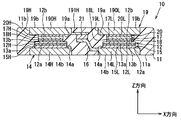
- 電子部品(12)と、
前記電子部品を封止する封止樹脂体(11)と、
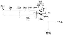
前記封止樹脂体の内部に配置されたインナーリード(250)と、前記インナーリードに連なり、前記封止樹脂体の外部に突出するアウターリード(251)と、を有し、前記封止樹脂体の内外にわたって延設されたリードフレーム(25)と、
前記封止樹脂体の内部において、前記電子部品と前記インナーリードとを電気的に接続するボンディングワイヤ(26)と、
を備え、
前記インナーリードが、金属材料を用いて形成された基材(252)と、前記基材の表面のうち、前記インナーリードにおける前記ボンディングワイヤが接続されるボンディング面(250a)側の表面に少なくとも形成された皮膜(253)と、を有し、
前記皮膜が、前記基材の表面に形成され、一部分に前記ボンディングワイヤが接続された金属薄膜(254)と、前記金属薄膜の主成分の金属と同じ金属の酸化物よりなり、前記金属薄膜上であって前記ボンディングワイヤの接続領域(250b)を除く部分の少なくとも一部に形成された酸化膜(255)と、を有し、
前記酸化膜が、表面が連続して凹凸をなす凹凸酸化膜(256)を含んでおり、
前記ボンディング面において、前記アウターリード側の端部とは反対の端部を先端部(250c)とすると、前記凹凸酸化膜が、前記接続領域よりも前記先端部側の領域である先端領域(250e)の少なくとも一部に形成されている電子装置。 - 前記凹凸酸化膜は、前記ボンディング面において前記先端部から形成されている請求項1に記載の電子装置。
- 前記アウターリード側の端部を後端部(250d)とすると、前記凹凸酸化膜は、前記ボンディング面において、前記接続領域よりも前記後端部側の領域である後端領域(250f)の少なくとも一部に形成されている請求項1又は請求項2に記載の電子装置。
- 前記リードフレームの延設方向に直交する幅方向において、前記凹凸酸化膜は、前記接続領域に並んで形成されており、
前記先端領域に形成された凹凸酸化膜と、前記接続領域に並んで形成された凹凸酸化膜と、前記後端領域に形成された凹凸酸化膜とが、一体的に連なっている請求項3に記載の電子装置。 - 前記凹凸酸化膜は、前記接続領域を取り囲んでいる請求項4に記載の電子装置。
- 前記金属薄膜は、前記凹凸酸化膜が形成された部分の表面に複数の凹部(254a)を有する請求項1〜5いずれか1項に記載の電子装置。
- 前記金属薄膜において、前記凹凸酸化膜が形成された部分の平均膜厚が、前記凹凸酸化膜が形成されていない部分の平均膜厚よりも薄くなっている請求項1〜6いずれか1項に記載の電子装置。
- 前記酸化膜は、前記凹凸酸化膜と前記接続領域との間で前記凹凸酸化膜に隣接して形成され、自然酸化膜よりも膜厚が厚く、前記凹凸酸化膜の平均膜厚よりも薄い中間酸化膜(257)を含む請求項1〜7いずれか1項に記載の電子装置。
- 前記金属薄膜は、Niを主成分とする請求項1〜8いずれか1項に記載の電子装置。
- 前記金属薄膜は、めっき膜である請求項9に記載の電子装置。
- 前記金属薄膜は、無電解めっき膜である請求項10に記載の電子装置。
- 電子部品(12)と、
前記電子部品を封止する封止樹脂体(11)と、
前記封止樹脂体の内部に配置されたインナーリード(250)と、前記インナーリードに連なり、前記封止樹脂体の外部に突出するアウターリード(251)と、を有し、前記封止樹脂体の内外にわたって延設されたリードフレーム(25)と、
前記封止樹脂体の内部において、前記電子部品と前記インナーリードとを電気的に接続するボンディングワイヤ(26)と、
を備え、
前記インナーリードが、金属材料を用いて形成された基材(252)と、前記基材の表面のうち、前記インナーリードにおける前記ボンディングワイヤが接続されるボンディング面(250a)側の表面に少なくとも形成された皮膜(253)と、を有し、
前記皮膜が、前記基材の表面に形成され、一部分に前記ボンディングワイヤが接続された金属薄膜(254)と、前記金属薄膜の主成分の金属と同じ金属の酸化物よりなり、前記金属薄膜上であって前記ボンディングワイヤの接続領域(250b)を除く部分の少なくとも一部に形成された酸化膜(255)と、を有し、
前記酸化膜が、表面が連続して凹凸をなす凹凸酸化膜(256)を含む電子装置の製造方法であって、
前記金属薄膜が形成された前記基材を準備し、
前記ボンディング面において、前記アウターリード側の端部とは反対の端部を先端部(250c)とすると、前記金属薄膜の表面のうち、前記接続領域よりも前記先端部側の領域である先端領域(250e)の少なくとも一部にパルス発振のレーザ光を照射して、前記凹凸酸化膜を形成し、
前記凹凸酸化膜の形成後、前記ボンディングワイヤを介して、前記電子部品と前記インナーリードとを接続し、
前記ボンディングワイヤ、前記電子部品、及び前記インナーリードを覆うように、前記封止樹脂体を成形する電子装置の製造方法。
Priority Applications (4)
| Application Number | Priority Date | Filing Date | Title |
|---|---|---|---|
| JP2016075388A JP6485397B2 (ja) | 2016-04-04 | 2016-04-04 | 電子装置及びその製造方法 |
| US15/772,116 US10236230B2 (en) | 2016-04-04 | 2017-03-13 | Electronic device and method for manufacturing the same |
| CN201780009036.8A CN108604579B (zh) | 2016-04-04 | 2017-03-13 | 电子装置及其制造方法 |
| PCT/JP2017/009857 WO2017175542A1 (ja) | 2016-04-04 | 2017-03-13 | 電子装置及びその製造方法 |
Applications Claiming Priority (1)
| Application Number | Priority Date | Filing Date | Title |
|---|---|---|---|
| JP2016075388A JP6485397B2 (ja) | 2016-04-04 | 2016-04-04 | 電子装置及びその製造方法 |
Publications (2)
| Publication Number | Publication Date |
|---|---|
| JP2017188534A JP2017188534A (ja) | 2017-10-12 |
| JP6485397B2 true JP6485397B2 (ja) | 2019-03-20 |
Family
ID=60000378
Family Applications (1)
| Application Number | Title | Priority Date | Filing Date |
|---|---|---|---|
| JP2016075388A Active JP6485397B2 (ja) | 2016-04-04 | 2016-04-04 | 電子装置及びその製造方法 |
Country Status (4)
| Country | Link |
|---|---|
| US (1) | US10236230B2 (ja) |
| JP (1) | JP6485397B2 (ja) |
| CN (1) | CN108604579B (ja) |
| WO (1) | WO2017175542A1 (ja) |
Families Citing this family (8)
| Publication number | Priority date | Publication date | Assignee | Title |
|---|---|---|---|---|
| JP6874467B2 (ja) * | 2017-03-29 | 2021-05-19 | 株式会社デンソー | 半導体装置とその製造方法 |
| JP2019083295A (ja) * | 2017-10-31 | 2019-05-30 | トヨタ自動車株式会社 | 半導体装置 |
| JP7154529B2 (ja) * | 2017-12-13 | 2022-10-18 | 株式会社デンソー | 金属部材および当該金属部材を用いた半導体素子、樹脂金属複合体、半導体装置、異種金属複合体並びに当該金属部材の製造方法 |
| JP6939679B2 (ja) * | 2018-03-29 | 2021-09-22 | 株式会社デンソー | 半導体装置 |
| CN115244684B (zh) * | 2020-03-11 | 2026-01-16 | 罗姆股份有限公司 | 半导体器件 |
| JP2023007028A (ja) * | 2021-07-01 | 2023-01-18 | ローム株式会社 | 半導体装置 |
| JP7761148B2 (ja) * | 2022-06-13 | 2025-10-28 | 富士電機株式会社 | 半導体装置 |
| JPWO2025115059A1 (ja) * | 2023-11-27 | 2025-06-05 |
Family Cites Families (12)
| Publication number | Priority date | Publication date | Assignee | Title |
|---|---|---|---|---|
| JPS6060742A (ja) * | 1983-09-14 | 1985-04-08 | Matsushita Electronics Corp | リ−ドフレ−ム |
| JP4378892B2 (ja) | 2001-03-19 | 2009-12-09 | 株式会社デンソー | リードフレームの製造方法 |
| JP2002299538A (ja) | 2001-03-30 | 2002-10-11 | Dainippon Printing Co Ltd | リードフレーム及びそれを用いた半導体パッケージ |
| US6882048B2 (en) | 2001-03-30 | 2005-04-19 | Dainippon Printing Co., Ltd. | Lead frame and semiconductor package having a groove formed in the respective terminals for limiting a plating area |
| DE10148120B4 (de) * | 2001-09-28 | 2007-02-01 | Infineon Technologies Ag | Elektronische Bauteile mit Halbleiterchips und ein Systemträger mit Bauteilpositionen sowie Verfahren zur Herstellung eines Systemträgers |
| JP4045985B2 (ja) | 2003-03-13 | 2008-02-13 | 株式会社デンソー | 樹脂封止型電子装置 |
| JP4472773B1 (ja) | 2009-01-06 | 2010-06-02 | 日電精密工業株式会社 | リードフレームの製造方法及びリードフレーム、ヒートシンクの製造方法及びヒートシンク |
| CN101916731B (zh) * | 2010-07-12 | 2012-07-04 | 深圳大学 | 一种陶瓷绝缘膜导热基板及其制作方法 |
| JP5669495B2 (ja) | 2010-09-17 | 2015-02-12 | 株式会社大貫工業所 | 樹脂封止金属部品、それに用いるリードフレーム、及び金属部品の製造方法 |
| JP5691831B2 (ja) * | 2011-05-18 | 2015-04-01 | 株式会社デンソー | 半導体装置およびその製造方法 |
| JP2013071312A (ja) | 2011-09-28 | 2013-04-22 | Hitachi Automotive Systems Ltd | 金属部材と成形樹脂部材との複合成形体および金属部材の表面加工方法 |
| US9899336B2 (en) * | 2014-04-04 | 2018-02-20 | Mitsubishi Electric Corporation | Semiconductor device |
-
2016
- 2016-04-04 JP JP2016075388A patent/JP6485397B2/ja active Active
-
2017
- 2017-03-13 CN CN201780009036.8A patent/CN108604579B/zh active Active
- 2017-03-13 WO PCT/JP2017/009857 patent/WO2017175542A1/ja not_active Ceased
- 2017-03-13 US US15/772,116 patent/US10236230B2/en active Active
Also Published As
| Publication number | Publication date |
|---|---|
| US10236230B2 (en) | 2019-03-19 |
| CN108604579B (zh) | 2022-03-18 |
| CN108604579A (zh) | 2018-09-28 |
| WO2017175542A1 (ja) | 2017-10-12 |
| JP2017188534A (ja) | 2017-10-12 |
| US20180323125A1 (en) | 2018-11-08 |
Similar Documents
| Publication | Publication Date | Title |
|---|---|---|
| JP6485397B2 (ja) | 電子装置及びその製造方法 | |
| JP6686691B2 (ja) | 電子装置 | |
| JP6485398B2 (ja) | 電子装置及びその製造方法 | |
| JP6578900B2 (ja) | 半導体装置及びその製造方法 | |
| JP5076440B2 (ja) | 半導体装置及び半導体装置の製造方法 | |
| JP4924411B2 (ja) | 電力半導体装置 | |
| US10943859B2 (en) | Semiconductor device | |
| WO2017154289A1 (ja) | 半導体装置及び半導体装置の製造方法 | |
| US11742256B2 (en) | Semiconductor device | |
| WO2016092791A1 (ja) | 半導体装置およびその製造方法 | |
| WO2018173511A1 (ja) | 半導体装置 | |
| WO2022249804A1 (ja) | 半導体装置 | |
| JP4765853B2 (ja) | 半導体装置の製造方法 | |
| WO2019187608A1 (ja) | 半導体装置 | |
| WO2022249814A1 (ja) | 半導体装置 | |
| JP2020198388A (ja) | 半導体装置およびその製造方法 | |
| WO2022249812A1 (ja) | 半導体装置 | |
| WO2022249803A1 (ja) | 半導体装置 | |
| WO2022249807A1 (ja) | 半導体装置 | |
| JP5151837B2 (ja) | 半導体装置の製造方法 | |
| JP2022185936A (ja) | 半導体装置 |
Legal Events
| Date | Code | Title | Description |
|---|---|---|---|
| A621 | Written request for application examination |
Free format text: JAPANESE INTERMEDIATE CODE: A621 Effective date: 20180214 |
|
| TRDD | Decision of grant or rejection written | ||
| A01 | Written decision to grant a patent or to grant a registration (utility model) |
Free format text: JAPANESE INTERMEDIATE CODE: A01 Effective date: 20190122 |
|
| A61 | First payment of annual fees (during grant procedure) |
Free format text: JAPANESE INTERMEDIATE CODE: A61 Effective date: 20190204 |
|
| R151 | Written notification of patent or utility model registration |
Ref document number: 6485397 Country of ref document: JP Free format text: JAPANESE INTERMEDIATE CODE: R151 |
|
| R250 | Receipt of annual fees |
Free format text: JAPANESE INTERMEDIATE CODE: R250 |
|
| R250 | Receipt of annual fees |
Free format text: JAPANESE INTERMEDIATE CODE: R250 |
|
| R250 | Receipt of annual fees |
Free format text: JAPANESE INTERMEDIATE CODE: R250 |
|
| R250 | Receipt of annual fees |
Free format text: JAPANESE INTERMEDIATE CODE: R250 |
|
| R250 | Receipt of annual fees |
Free format text: JAPANESE INTERMEDIATE CODE: R250 |