JP6483997B2 - Power semiconductor drive circuit, power semiconductor circuit, and power module circuit device - Google Patents
Power semiconductor drive circuit, power semiconductor circuit, and power module circuit device Download PDFInfo
- Publication number
- JP6483997B2 JP6483997B2 JP2014208662A JP2014208662A JP6483997B2 JP 6483997 B2 JP6483997 B2 JP 6483997B2 JP 2014208662 A JP2014208662 A JP 2014208662A JP 2014208662 A JP2014208662 A JP 2014208662A JP 6483997 B2 JP6483997 B2 JP 6483997B2
- Authority
- JP
- Japan
- Prior art keywords
- circuit
- power semiconductor
- transistor
- gate
- time
- Prior art date
- Legal status (The legal status is an assumption and is not a legal conclusion. Google has not performed a legal analysis and makes no representation as to the accuracy of the status listed.)
- Active
Links
- 239000004065 semiconductor Substances 0.000 title claims description 142
- 238000012544 monitoring process Methods 0.000 claims description 91
- 239000003990 capacitor Substances 0.000 claims description 21
- 239000000758 substrate Substances 0.000 claims description 9
- JMASRVWKEDWRBT-UHFFFAOYSA-N Gallium nitride Chemical compound [Ga]#N JMASRVWKEDWRBT-UHFFFAOYSA-N 0.000 claims description 6
- HBMJWWWQQXIZIP-UHFFFAOYSA-N silicon carbide Chemical compound [Si+]#[C-] HBMJWWWQQXIZIP-UHFFFAOYSA-N 0.000 claims description 5
- XUIMIQQOPSSXEZ-UHFFFAOYSA-N Silicon Chemical compound [Si] XUIMIQQOPSSXEZ-UHFFFAOYSA-N 0.000 claims description 4
- 230000010354 integration Effects 0.000 claims description 4
- 229910052710 silicon Inorganic materials 0.000 claims description 4
- 239000010703 silicon Substances 0.000 claims description 4
- 230000000295 complement effect Effects 0.000 claims description 3
- 230000009977 dual effect Effects 0.000 claims description 3
- 239000000463 material Substances 0.000 claims 2
- 230000015556 catabolic process Effects 0.000 description 16
- 230000007704 transition Effects 0.000 description 15
- 230000003111 delayed effect Effects 0.000 description 9
- 238000010586 diagram Methods 0.000 description 9
- 230000000694 effects Effects 0.000 description 7
- 230000001052 transient effect Effects 0.000 description 7
- 230000007423 decrease Effects 0.000 description 6
- 101150110971 CIN7 gene Proteins 0.000 description 4
- 101150110298 INV1 gene Proteins 0.000 description 4
- 101100397044 Xenopus laevis invs-a gene Proteins 0.000 description 4
- 230000008859 change Effects 0.000 description 4
- 230000006866 deterioration Effects 0.000 description 3
- 230000007257 malfunction Effects 0.000 description 3
- 238000000034 method Methods 0.000 description 3
- 238000004804 winding Methods 0.000 description 3
- RYGMFSIKBFXOCR-UHFFFAOYSA-N Copper Chemical compound [Cu] RYGMFSIKBFXOCR-UHFFFAOYSA-N 0.000 description 2
- 229910002601 GaN Inorganic materials 0.000 description 2
- 230000002159 abnormal effect Effects 0.000 description 2
- 229910052782 aluminium Inorganic materials 0.000 description 2
- XAGFODPZIPBFFR-UHFFFAOYSA-N aluminium Chemical compound [Al] XAGFODPZIPBFFR-UHFFFAOYSA-N 0.000 description 2
- 229910052802 copper Inorganic materials 0.000 description 2
- 239000010949 copper Substances 0.000 description 2
- 238000006731 degradation reaction Methods 0.000 description 2
- 230000007274 generation of a signal involved in cell-cell signaling Effects 0.000 description 2
- 230000009191 jumping Effects 0.000 description 2
- 230000004048 modification Effects 0.000 description 2
- 238000012986 modification Methods 0.000 description 2
- 230000004044 response Effects 0.000 description 2
- 230000000630 rising effect Effects 0.000 description 2
- 230000008054 signal transmission Effects 0.000 description 2
- 230000001629 suppression Effects 0.000 description 2
- 238000013459 approach Methods 0.000 description 1
- 238000012790 confirmation Methods 0.000 description 1
- 230000006378 damage Effects 0.000 description 1
- 230000001934 delay Effects 0.000 description 1
- 238000001514 detection method Methods 0.000 description 1
- 230000005669 field effect Effects 0.000 description 1
- 230000012447 hatching Effects 0.000 description 1
- 229910044991 metal oxide Inorganic materials 0.000 description 1
- 150000004706 metal oxides Chemical class 0.000 description 1
- 230000003071 parasitic effect Effects 0.000 description 1
- 230000002093 peripheral effect Effects 0.000 description 1
- 230000002265 prevention Effects 0.000 description 1
Images


Classifications
-
- H—ELECTRICITY
- H03—ELECTRONIC CIRCUITRY
- H03K—PULSE TECHNIQUE
- H03K19/00—Logic circuits, i.e. having at least two inputs acting on one output; Inverting circuits
- H03K19/0008—Arrangements for reducing power consumption
- H03K19/0016—Arrangements for reducing power consumption by using a control or a clock signal, e.g. in order to apply power supply
-
- H—ELECTRICITY
- H03—ELECTRONIC CIRCUITRY
- H03K—PULSE TECHNIQUE
- H03K17/00—Electronic switching or gating, i.e. not by contact-making and –breaking
- H03K17/16—Modifications for eliminating interference voltages or currents
- H03K17/161—Modifications for eliminating interference voltages or currents in field-effect transistor switches
- H03K17/162—Modifications for eliminating interference voltages or currents in field-effect transistor switches without feedback from the output circuit to the control circuit
- H03K17/163—Soft switching
-
- H—ELECTRICITY
- H03—ELECTRONIC CIRCUITRY
- H03K—PULSE TECHNIQUE
- H03K17/00—Electronic switching or gating, i.e. not by contact-making and –breaking
- H03K17/16—Modifications for eliminating interference voltages or currents
- H03K17/161—Modifications for eliminating interference voltages or currents in field-effect transistor switches
- H03K17/162—Modifications for eliminating interference voltages or currents in field-effect transistor switches without feedback from the output circuit to the control circuit
Description
本発明は、パワー半導体駆動回路、及びそれを用いたパワー半導体回路、及びパワー半導体回路と他の回路装置とを1つの組立体に搭載したパワーモジュール回路装置に関する。 The present invention relates to a power semiconductor drive circuit, a power semiconductor circuit using the power semiconductor circuit, and a power module circuit device in which the power semiconductor circuit and another circuit device are mounted in one assembly.
パワー半導体素子としては、たとえば、IGBT(Insulated Gate Bipolar Transistor)や、パワーMOSトランジスタ(Metal Oxide Semiconductor Field Effect Transistor)、あるいは、MOSGTO(MOS Gate Turn-off Thyristor )等が知られている。また、これらのパワー半導体素子と、そのパワー半導体素子のゲートを制御するパワー半導体駆動回路とを一体化したパワー半導体回路、及びこのパワー半導体回路と他の回路装置を1つの実装体に組み込んだインテリジェント・パワー・モジュール(IPM:Intelligent Power Module )(以下IPM)も広く知られている。 Known power semiconductor elements include IGBTs (Insulated Gate Bipolar Transistors), power MOS transistors (Metal Oxide Semiconductor Field Effect Transistors), MOSGTOs (MOS Gate Turn-off Thyristors), and the like. In addition, a power semiconductor circuit in which these power semiconductor elements and a power semiconductor drive circuit for controlling the gate of the power semiconductor element are integrated, and an intelligent in which this power semiconductor circuit and another circuit device are incorporated in one mounting body. A power module (IPM: Intelligent Power Module) (hereinafter IPM) is also widely known.
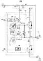
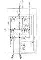
図11に従来のパワー半導体駆動回路、パワー半導体回路、及びパワーモジュール回路装置を模式的に示す。図11では、トランジスタM2とM3のドレインD同士が共通に接続され、この共通接続点はノードHOとトランジスタPT1のゲートGに接続される。トランジスタM2,M3のゲートG同士は共通に接続され、これらの共通ゲートGには上側ドライバUDを介して上側入力信号HINが印加される。トランジスタM2のソースSには外部端子VDを介して電源電圧VBBが印加される。電源電圧VBBは外部端子VCに供給される電源電圧VCCとブートストラップ回路BSで生成されたブースト電圧である。トランジスタM3のソースSはノードVSに接続される。 FIG. 11 schematically shows a conventional power semiconductor drive circuit, power semiconductor circuit, and power module circuit device. In FIG. 11, the drains D of the transistors M2 and M3 are connected in common, and this common connection point is connected to the node HO and the gate G of the transistor PT1. The gates G of the transistors M2 and M3 are connected in common, and the upper input signal HIN is applied to these common gates G via the upper driver UD. A power supply voltage VBB is applied to the source S of the transistor M2 via the external terminal VD. The power supply voltage VBB is a boost voltage generated by the power supply voltage VCC supplied to the external terminal VC and the bootstrap circuit BS. The source S of the transistor M3 is connected to the node VS.
トランジスタPT1は上側パワートランジスタと称し、そのドレインDには外部端子Pを介して電源電圧VPPが印加される。トランジスタPT1のゲートGはノードHOに接続される。トランジスタPT1のソースSはノードVSに接続される。トランジスタPT1のソースSとドレインDとの間には、還流用のダイオード(符号なし)が接続される。 The transistor PT1 is referred to as an upper power transistor, and the power supply voltage VPP is applied to its drain D via the external terminal P. The gate G of the transistor PT1 is connected to the node HO. The source S of the transistor PT1 is connected to the node VS. Between the source S and the drain D of the transistor PT1, a free-wheeling diode (no symbol) is connected.
トランジスタPT2は一般的に下側パワートランジスタと称され、上側パワートランジスタと称されるトランジスタPT1とは別の半導体基板上に作り込まれている。トランジスタPT1とトランジスタPT2を接続する接続体はアルミニウムや銅などを材料としたワイヤーLWが使用されている。ワイヤーLWの第1端はノードVSに、その第2端は出力端子OUT及びトランジスタPT2のドレインDにそれぞれ接続される。ワイヤーLWはインダクタンス成分lwを有する。 The transistor PT2 is generally referred to as a lower power transistor, and is formed on a different semiconductor substrate from the transistor PT1 referred to as an upper power transistor. A wire LW made of aluminum, copper, or the like is used as a connection body that connects the transistor PT1 and the transistor PT2. The wire LW has a first end connected to the node VS and a second end connected to the output terminal OUT and the drain D of the transistor PT2. The wire LW has an inductance component lw.
トランジスタPT2のドレインDは、出力端子OUTに接続され、そのソースSは外部端子Nを介して接地電位GNDに接続され、そのゲートGには下側入力信号LINが印加される。トランジスタPT2のソースSとドレインDとの間には、トランジスタPT1と同様に還流用のダイオード(符号なし)が接続されている。トランジスタPT2はトランジスタPT1と相補的にオン、オフする。したがって、トランジスタPT2がオンであるときトランジスタPT1はオフであり、トランジスタPT2がオフであるときトランジスタPT1はオンとなるように制御される。 The drain D of the transistor PT2 is connected to the output terminal OUT, the source S is connected to the ground potential GND via the external terminal N, and the lower input signal LIN is applied to the gate G. Between the source S and the drain D of the transistor PT2, a free-wheeling diode (not shown) is connected as in the transistor PT1. The transistor PT2 is turned on / off complementarily with the transistor PT1. Therefore, the transistor PT1 is controlled to be off when the transistor PT2 is on, and the transistor PT1 is controlled to be on when the transistor PT2 is off.
外部端子VCと外部端子OUTの間にブートストラップ用のキャパシタCBが接続される。外部端子OUTは外部負荷と接続される。外部負荷として、インダクタL1を示している。インダクタL1はインバータに用いるたとえば三相巻線、モータ巻線、及びスイッチングレギュレータに採用されるインダクタを端的に示したものである。 A bootstrap capacitor CB is connected between the external terminal VC and the external terminal OUT. The external terminal OUT is connected to an external load. An inductor L1 is shown as an external load. The inductor L1 simply indicates an inductor employed in, for example, a three-phase winding, a motor winding, and a switching regulator used in an inverter.
図11に示した従来のパワー半導体駆動回路等ではトランジスタPT1のスイッチング速度が速いとワイヤーLWが有するインダクタ成分lwによって過渡電圧ΔVが発生し、トランジスタM2,M3が劣化または破壊するという不具合が生じうる。また、トランジスタPT2のスイッチング速度が速いと、トランジスタPT1のゲート容量Crss及びCissが充電され、トランジスタPT1のゲート電圧がその閾値電圧Vthを超えてしまい、本来オフ状態に置かれるべきであるトランジスタPT1がセルフターンオンしてしまい、トランジスタPT1とトランジスタPT2の間に貫通電流が流れ、トランジスタPT1,PT2が劣化するという懸念が生じる。また、劣化に至らなくとも無駄な電力を消費してしまい、省電力化が実現できないという懸念が生じる。 In the conventional power semiconductor drive circuit shown in FIG. 11 and the like, when the switching speed of the transistor PT1 is fast, a transient voltage ΔV is generated by the inductor component lw of the wire LW, which may cause a problem that the transistors M2 and M3 are deteriorated or destroyed. . Further, when the switching speed of the transistor PT2 is fast, the gate capacitances Crss and Ciss of the transistor PT1 are charged, the gate voltage of the transistor PT1 exceeds the threshold voltage Vth, and the transistor PT1 that should originally be placed in the off state There is a concern that self-turn-on occurs, a through current flows between the transistors PT1 and PT2, and the transistors PT1 and PT2 deteriorate. Moreover, even if it does not lead to deterioration, wasteful power is consumed, and there is a concern that power saving cannot be realized.
上記問題の解決策として、特許文献1はターンオン時のゲート電圧がミラー電圧に到達した時、並列回路のスイッチング素子を切り換えて、電圧駆動型素子の駆動能力を低くするようにしている。
As a solution to the above problem,
特許文献2はゲート電圧の変化を比較回路で検出し、それに応じてゲート抵抗を変化させる方法を開示する。 Patent Document 2 discloses a method of detecting a change in gate voltage with a comparison circuit and changing the gate resistance accordingly.
特許文献3はEMIノイズの抑制と、スイッチング損失の抑制の両立を低コストで実現するパワーデバイス制御回路を提供するとしている。その1つの実施形態として、ゲート電圧がミラー電圧に到達するまでの時間と等しくなるように抵抗素子とキャパシタから成る時定数回路をタイマー回路として採用する技術的思想を示唆する。 Patent document 3 is to provide a power device control circuit that realizes both suppression of EMI noise and suppression of switching loss at low cost. As one embodiment thereof, a technical idea is suggested in which a time constant circuit including a resistance element and a capacitor is adopted as a timer circuit so that the gate voltage becomes equal to the time until the mirror voltage is reached.
しかし、特許文献1ではオン状態からオフ状態へのスイッチング動作に伴って発生するサージ、過渡電圧によるゲートドライバに耐圧破壊の危険性が依然として残る。
However, in
また、特許文献2は高電位側素子がオフからオンに切り替わる時またはオフからオンに切り替わる時を検出し、それを応じて予め定められた電圧値を設定するための比較的複雑なタイマー回路が必要とされる。 Patent Document 2 discloses a relatively complicated timer circuit for detecting when the high-potential side element is switched from OFF to ON or when switching from OFF to ON, and setting a predetermined voltage value accordingly. Needed.
また、特許文献3は、EMIノイズを抑制するとしているが、パワー半導体駆動回路の耐圧破壊や、パワー半導体のスイッチング損失を抑制することは期待できない。 Moreover, although patent document 3 is trying to suppress EMI noise, it cannot be expected to suppress breakdown voltage breakdown of the power semiconductor drive circuit or switching loss of the power semiconductor.
本発明は、上記の問題点に鑑み、高電圧大電流での高速スイッチング化に伴い、特にオン状態からオフ状態時すなわち、ターンオフ時にワイヤーが有するインダクタンス成分によって生じる誘起電圧、過渡電圧、跳ね上がり電圧等によってゲートドライバ耐圧破壊を防ぐとともに、パワートランジスタのセルフターンオンを抑止し、スイッチング損失を抑制することができるパワー半導体駆動回路、パワー半導体回路、及びパワーモジュール回路装置を提供することを目的とする。 In view of the above-mentioned problems, the present invention is accompanied by high-speed switching with high voltage and large current, and particularly induced voltage, transient voltage, jumping voltage, etc. generated by the inductance component of the wire at the time of turn-off from the on-state. An object of the present invention is to provide a power semiconductor drive circuit, a power semiconductor circuit, and a power module circuit device that can prevent breakdown of the gate driver breakdown voltage, suppress self-turn-on of the power transistor, and suppress switching loss.
本発明にかかる一実施の態様のパワー半導体駆動回路は、パワー半導体素子のゲート側に接続され、パワー半導体素子のゲート抵抗を設定する少なくとも2つのトランジスタで構成した並列回路と、パワー半導体素子のゲート側及び並列回路に接続されパワー半導体素子のゲート電圧を監視するために所定の監視電圧が設定されたゲート電圧監視回路を備える。また、ゲート電圧監視回路からの出力信号を遅延させる信号遅延回路と、信号遅延回路側から出力される出力信号に基づき並列回路の合成抵抗の大きさを切り換えるゲートコントロール回路とを備えている。 A power semiconductor drive circuit according to an embodiment of the present invention includes a parallel circuit that is connected to a gate side of a power semiconductor element and includes at least two transistors that set a gate resistance of the power semiconductor element, and a gate of the power semiconductor element. And a gate voltage monitoring circuit which is connected to the side and parallel circuits and has a predetermined monitoring voltage set for monitoring the gate voltage of the power semiconductor element. In addition, a signal delay circuit that delays the output signal from the gate voltage monitoring circuit and a gate control circuit that switches the magnitude of the combined resistance of the parallel circuit based on the output signal output from the signal delay circuit side are provided.
また本発明にかかる別の実施の態様であるパワー半導体回路は、上記のパワー半導体駆動回路と、パワー半導体駆動回路で駆動されるパワー半導体素子を備える。パワー半導体素子は、MOSトランジスタ、IGBTが用いられる。MOSトランジスタ、IGBTはシリコン(Si)、シリコンカーバイド(SiC)、ガリウムナイトライド(GaN)のいずれか1つを材料とする。 A power semiconductor circuit according to another embodiment of the present invention includes the above power semiconductor drive circuit and a power semiconductor element driven by the power semiconductor drive circuit. As the power semiconductor element, a MOS transistor or IGBT is used. The MOS transistor and IGBT are made of silicon (Si), silicon carbide (SiC), or gallium nitride (GaN).
また本発明にかかる別の実施の態様であるパワーモジュール回路装置は、上記パワー半導体回路に加えて、少なくともブートストラップ回路を備えている。こうしたパワーモジュール回路装置は、1つのデュアルライン型パッケージに実装され小型化されている。 A power module circuit device according to another embodiment of the present invention includes at least a bootstrap circuit in addition to the power semiconductor circuit. Such a power module circuit device is miniaturized by being mounted in one dual line type package.
本発明によれば、高電圧大電流での高速スイッチング化に伴い、特にオン状態からオフ状態時の内部インダクタンスによるゲートドライバの劣化、耐圧破壊を防ぎ、且つオフからオン時のセルフターンオンをスイッチング損失の低減化が図れる。 According to the present invention, with high-speed switching at high voltage and large current, deterioration of the gate driver due to internal inductance from the on-state to the off-state, prevention of breakdown voltage, and self-turn-on from off to on are prevented. Can be reduced.
(第1実施形態)
図1は本発明に係るパワー半導体駆動回路、パワー半導体回路、及びパワーモジュール回路装置を示す。パワー半導体回路10Aはパワー半導体駆動回路10を含み、パワーモジュール回路装置100はパワー半導体回路10Aを含む。言い換えれば、パワー半導体駆動回路10にトランジスタPT1,PT2を加えた回路構成でパワー半導体回路10Aを構成する。また、パワー半導体回路10Aに少なくともブートストラップ回路BSを加えた回路構成でパワーモジュール回路装置100を構成している。パワーモジュール回路装置100はIPMと称することができる。なお、ブートストラップ回路BSはダイオードDB及びキャパシタCBの両方をパワーモジュール回路装置100に内蔵せずに、たとえばダイオードDBのみの電子素子を内蔵し、キャパシタCBはパワーモジュール回路装置100の外部に配置させることもできる。また、ブートストラップ回路BSはダイオード、キャパシタだけではなく、抵抗、トランジスタ、スイッチング素子、電流源等の電子素子を用いて構成してもよい。
(First embodiment)
FIG. 1 shows a power semiconductor drive circuit, a power semiconductor circuit, and a power module circuit device according to the present invention. The
パワーモジュール回路装置、すなわちIPMは一般的に半導体基板上に作り込まれた各種ICとダイオード、抵抗、インダクタ、パワートランジスタ等の個別部品が1つの実装体に組み込まれた1つのICと見ることができる。図1では、パワー半導体駆動回路10は半導体基板上に作り込まれた1つまたは複数のICで構成される。トランジスタPT1,PT2は、パワー半導体駆動回路10によって、そのゲートGが制御される。トランジスタPT1,PT2は、パワー半導体駆動回路10とは別の半導体基板上に作り込まれた能動素子であり、また個別部品でもある。本発明の実施形態ではトランジスタPT1とトランジスタPT2はそれぞれ別々の半導体基板上に形成したが、両者を同一の半導体基板上に形成してもよい。ブートストラップ回路BSに用いられるダイオード、キャパシタそれぞれは、パワー半導体駆動回路10及びトランジスタPT1,PT2とは別の基板上に作り込まれた受動素子であり、また個別部品でもある。
A power module circuit device, i.e., IPM, is generally seen as a single IC in which various ICs built on a semiconductor substrate and individual components such as diodes, resistors, inductors, and power transistors are incorporated in a single mounting body. it can. In FIG. 1, the power
図1に示したパワーモジュール回路装置100は、第1電源端子としての外部端子VC、第2電源端子としての外部端子P、出力端子としての外部端子OUT、接地端子としての外部端子N等の外部端子を備える。また、上側ドライバUDを駆動するためにブーストした電圧を供給する外部端子VBも備える。これらの外部端子のほかにも図示しないMCUから供給される上側入力信号HINや下側入力信号LINが入力される外部端子も備えている。
The power
パワーモジュール回路装置100は、前に述べたようにICと、その他個別部品とを組み合わせて1つの実装体で構成されているので、外見上は1つのICとみなすことができる。パワーモジュール回路装置100は、実装体の対向する2つの側辺に外部端子が配置された、いわゆるデュアルライン型パッケージ(DIPと称する)に組み込まれている。DIPに実装することでパワーモジュール回路装置100の小型化が実現される。また、DIPに実装することにより、外部端子が配置されない側面側を配線領域として有効に利用することができる。
As described above, the power
トランジスタPT1,PT2には、パワー半導体素子として、たとえばパワーMOSトランジスタ、IGBTが採用される。たとえばパワーMOSトランジスタが作り込まれる半導体基板は、シリコン(Si)だけではなく、たとえばシリコンカーバイド(SiC)やGaN(ガリウムナイトライド)を用いることができる。 For example, a power MOS transistor or IGBT is employed as the power semiconductor element for transistors PT1 and PT2. For example, not only silicon (Si) but also silicon carbide (SiC) or GaN (gallium nitride) can be used as a semiconductor substrate on which a power MOS transistor is formed.
トランジスタPT1とトランジスタPT2はパワー半導体素子として用意されるが、その回路動作の役割は異なる。トランジスタPT1は負荷として示したインダクタL1に負荷電流を供給する役割があり、トランジスタPT2はトランジスタPT1とは別の上側パワートランジスタからインダクタL1に供給される負荷電流を引き込む役割を担う。トランジスタPT1及びPT2は一般的にそれぞれ上側パワートランジスタ及び下側パワートランジスタと称されることは前に述べたが、「上側」なる意味合いは、トランジスタPT1は電源端子側に、「下側」なる意味合いは接地端子側にそれぞれ接続されるからであり、回路構成図においても一般的に上側パワートランジスタは回路図を正視しての上側に、下側パワートランジスタは下側にそれぞれ配置されることが少なくない。 The transistors PT1 and PT2 are prepared as power semiconductor elements, but the roles of their circuit operations are different. The transistor PT1 has a role of supplying a load current to the inductor L1 shown as a load, and the transistor PT2 has a role of drawing a load current supplied to the inductor L1 from an upper power transistor different from the transistor PT1. As described above, the transistors PT1 and PT2 are generally referred to as an upper power transistor and a lower power transistor, respectively. However, the meaning of “upper” means that the transistor PT1 means “lower” on the power supply terminal side. Are generally connected to the ground terminal side, and generally in the circuit configuration diagram, the upper power transistor is generally arranged on the upper side of the circuit diagram and the lower power transistor is arranged on the lower side. Absent.
図1に示したトランジスタPT1,PT2はいずれもが導電形式がNMOSトランジスタで構成される。トランジスタPT1のドレインDは第2電源端子としての外部端子Pに接続され、そのソースSはトランジスタPT2のドレインDに接続され、これら共通接続点は出力端子OUTに接続される。トランジスタPT2のソースSは外部端子Nを介して接地電位GNDに接続される。なお、トランジスタPT2のソースSを直接、接地電位GNDに接続せずに電流検出抵抗を介して接地電位GNDに接続するようにしてもよい。トランジスタPT2のゲートGには下側ドライバLDを介して下側入力信号LINが印加される。また、トランジスタPT1,PT2の各ドレインDとソースS間にはそれぞれ還流ダイオード(無符号)が形成される。一般的に還流ダイオードはトランジスタPT1,PT2に寄生的に形成されるいわゆる寄生ダイオードを利用することができる。 Each of the transistors PT1 and PT2 shown in FIG. 1 is formed of an NMOS transistor in terms of conductivity. The drain D of the transistor PT1 is connected to the external terminal P as the second power supply terminal, the source S is connected to the drain D of the transistor PT2, and these common connection points are connected to the output terminal OUT. The source S of the transistor PT2 is connected to the ground potential GND through the external terminal N. Note that the source S of the transistor PT2 may be directly connected to the ground potential GND via the current detection resistor instead of being connected to the ground potential GND. The lower input signal LIN is applied to the gate G of the transistor PT2 via the lower driver LD. In addition, free-wheeling diodes (unsigned) are formed between the drains D and sources S of the transistors PT1 and PT2, respectively. In general, a so-called parasitic diode formed parasitically on the transistors PT1 and PT2 can be used as the freewheeling diode.
トランジスタPT1とPT2は相補的に動作する。すなわち、トランジスタPT1がオンの時トランジスタPT2はオフであり、トランジスタPT2がオンの時トランジスタPT1はオフになるようにトランジスタPT1とPT2の各ゲートGに印加される駆動信号の極性が設定される。なお、トランジスタPT1とPT2との間に貫通電流が流れ、両トランジスタが劣化または破壊しないように両トランジスタが同時にオフとなる、いわゆるデッドタイムが設定される。 Transistors PT1 and PT2 operate complementarily. That is, the polarity of the drive signal applied to each gate G of the transistors PT1 and PT2 is set so that the transistor PT2 is off when the transistor PT1 is on and the transistor PT1 is off when the transistor PT2 is on. Note that a so-called dead time is set in which a through current flows between the transistors PT1 and PT2, and both transistors are simultaneously turned off so that the two transistors are not deteriorated or destroyed.
トランジスタPT1のソースSとトランジスタPT2のドレインDは共通に接続され、その共通接続点は出力端子OUTに接続される。前に述べたが、本発明の一実施形態ではトランジスタPT1のソースSとトランジスタPT2のドレインDとはアルミニウムや銅などを材料としたワイヤーLWで接続される。ワイヤーLWはインダクタンス成分lwを有する。出力端子OUTにはたとえば、直流を交流に変換するためのインバータや、たとえば三相モータの三相巻線、あるいはスイッチングレギュレータ等のインダクタL1が結合される。インダクタL1は広義的には外部負荷とみるべきである。 The source S of the transistor PT1 and the drain D of the transistor PT2 are connected in common, and the common connection point is connected to the output terminal OUT. As described above, in one embodiment of the present invention, the source S of the transistor PT1 and the drain D of the transistor PT2 are connected by a wire LW made of aluminum, copper, or the like. The wire LW has an inductance component lw. For example, an inverter for converting DC to AC, an inductor L1 such as a three-phase winding of a three-phase motor, or a switching regulator is coupled to the output terminal OUT. The inductor L1 should be regarded as an external load in a broad sense.
パワー半導体駆動回路10Aは、トランジスタM2,M3,M4、ゲート電圧監視回路5、信号遅延回路6、ゲートコントロール回路7等を集積化した1つのICで構成される。
The power
トランジスタM2はPMOSトランジスタであり、トランジスタM3及びトランジスタM4はNMOSトランジスタである。トランジスタM2とトランジスタM3はトランジスタPT1を駆動するゲートドライバの役目を担う。トランジスタM3,M4はともにNMOSトランジスタで構成され、両トランジスタのドレインD−ソースSの導電路は互いに並列に接続され、さらにトランジスタPT1のゲートG−ソースSの導電路とも並列に接続されている。トランジスタM3,M4を含む少なくとも2つのトランジスタで構成される並列回路はトランジスタPT1がオフしている時のゲート抵抗を設定する。もちろん、ゲート抵抗値を調整するために、トランジスタM3及びM4の少なくとも一方側のソースS側またはドレインD側に抵抗を直列に接続してもかまわない。トランジスタM3がオンでトランジスタM4がオフの時の合成抵抗は、トランジスタM3のオン抵抗にほぼ等しい。トランジスタM3とトランジスタM4の両者が同時にオンしている時の合成抵抗は、トランジスタM3とトランジスタM4のオン抵抗の並列抵抗値となる、トランジスタM3,M4が同時にオンしている時の合成抵抗値は、トランジスタM3のみがオンした時のそれに比べて小さくなる。なお、トランジスタPT1がオフしている時のゲート抵抗を切り替えるにはトランジスタM3,M4の並列回路だけではなく、抵抗素子とトランジスタとを並列あるいは直列に接続しておき、抵抗値を切り替えることもできる。 The transistor M2 is a PMOS transistor, and the transistors M3 and M4 are NMOS transistors. The transistors M2 and M3 serve as gate drivers that drive the transistor PT1. The transistors M3 and M4 are both NMOS transistors, and the drain D-source S conductive paths of both transistors are connected in parallel to each other, and the gate G-source S conductive path of the transistor PT1 is also connected in parallel. A parallel circuit including at least two transistors including the transistors M3 and M4 sets a gate resistance when the transistor PT1 is off. Of course, in order to adjust the gate resistance value, a resistor may be connected in series to the source S side or the drain D side of at least one of the transistors M3 and M4. The combined resistance when the transistor M3 is on and the transistor M4 is off is approximately equal to the on-resistance of the transistor M3. The combined resistance when both the transistor M3 and the transistor M4 are simultaneously turned on is the parallel resistance value of the on-resistance of the transistor M3 and the transistor M4. The combined resistance when the transistors M3 and M4 are simultaneously turned on is This is smaller than that when only the transistor M3 is turned on. In order to switch the gate resistance when the transistor PT1 is off, not only the parallel circuit of the transistors M3 and M4 but also a resistance element and a transistor can be connected in parallel or in series to switch the resistance value. .
トランジスタM2のソースSは第1電源端子としての外部端子VCと接続される。トランジスタM2のドレインDは、トランジスタM3のドレインDと共通接続され、その共通接続点HOはトランジスタPT1のゲートGに接続される。トランジスタM2のゲートGはトランジスタM3のゲートGと共通接続され、その共通接続点HBはインバータINV1の出力に接続され、インバータINV1の入力には上側ドライバUDを介して上側入力信号HINが入力される。上側入力信号HINはトランジスタPT1のゲートGに印加される駆動信号となる。 A source S of the transistor M2 is connected to an external terminal VC as a first power supply terminal. The drain D of the transistor M2 is commonly connected to the drain D of the transistor M3, and the common connection point HO is connected to the gate G of the transistor PT1. The gate G of the transistor M2 is connected in common with the gate G of the transistor M3, the common connection point HB is connected to the output of the inverter INV1, and the upper input signal HIN is input to the input of the inverter INV1 via the upper driver UD. . The upper input signal HIN is a drive signal applied to the gate G of the transistor PT1.
トランジスタPT1のオフ時のゲート抵抗はトランジスタPT1,PT2のスイッチング特性消費電力、パワー半導体回路10A,パワーモジュール回路装置100の消費電力、トランジスタM2,M3で構成されるゲートドライバの耐圧に大きく関与してくる。ゲート抵抗が小さければ、トランジスタPT1のスイッチング特性は速くなり、消費電力も小さくなるが、トランジスタM2,M3の耐圧には不利となる。一方、ゲート抵抗が高くなると、トランジスタPT1のスイッチング特性は遅くなり、消費電力は大きくなるが、トランジスタM2,M3の耐圧には有利に働くことになる。
The gate resistance when the transistor PT1 is off is greatly related to the switching characteristic power consumption of the transistors PT1 and PT2, the power consumption of the
ゲート電圧監視回路5は共通接続点HO、すなわちトランジスタPT1のゲートG側に接続される。ゲート電圧監視回路5のオン、オフはゲート電圧監視回路5側に設定した所定の監視電圧Vkに基づき実行される。ここで、監視電圧VkはトランジスタPT1のミラー期間に生じるミラー電圧Vm以下に設定される。監視電圧Vkの設定は極めて重要な事項の1つである。なぜならば、監視電圧Vkの大きさは、トランジスタPT1のゲート抵抗の切替えタイミングを決めるからである。仮に監視電圧Vkをミラー電圧Vm以上に設定すると、トランジスタPT1のdi/dt(電流の時間変化率)が大きくなり、ワイヤーLWが有するインダクタンス成分lw等によって生じる跳ね上がり電圧(誘起電圧、過渡電圧)がトランジスタM2,M3の耐圧を超えてしまうという不具合が生じうる。なお、ミラー電圧Vmの大きさやミラー期間の長さはトランジスタPT1,PT2に採用されるパワー半導体素子の種類、導電形式、トランジスタのサイズ等によって異なってくる。また、同じ導電形式であってある程度ばらつきが生じる。さらに周辺回路構成や実装状況、使用温度等の動作条件によりミラー電圧Vmは変化するので、実施上ではある程度の余裕度をとる必要がある。
The gate
ゲート電圧監視回路5の出力信号V5は信号遅延回路6に入力される。信号遅延回路6は出力信号V5に含まれるノイズ成分によって後段の回路が本来の回路動作から逸脱しないために用意されている。また、信号遅延回路6は、信号伝達の遅延時間を決める機能も有し、トランジスタPT1がオンからオフへ遷移する時、トランジスタPT1のドレイン・ソース間に流れるドレイン・ソース電流id(以下、出力電流idと称する)が0になった後、トランジスタPT1のゲート抵抗値を変化することを保障する。
The output signal V5 of the gate
信号遅延回路6の出力信号V6及び上側入力信号HINの反転信号HINBは各別にゲートコントロール回路7に入力される。ゲートコントロール回路7の出力信号V7はトランジスタM4のゲートGに入力され、トランジスタM4をオン、オフさせる。たとえば出力信号V7がハイレベルH及びローレベルLの時にトランジスタM4はそれぞれオン及びオフになる。
The output signal V6 of the
ゲートコントロール回路7は信号遅延回路6の回路動作を補完する作用も有する。すなわち、ノイズ成分をさらに抑圧、除去する働きを有する。ノイズ成分を抑圧、除去するためにゲートコントロール回路7には閾値電圧Vzが設定される。出力信号V6が閾値電圧Vzを下回ると出力信号V7はハイレベルHとなり、トランジスタM4をオンさせトランジスタPT1のオフ時のゲート抵抗を下げる。
The
第1実施形態ではゲート電圧監視回路5、信号遅延回路6、ゲートコントロール回路7、及びトランジスタM4を上側パワートランジスタであるトランジスタPT1側に設けたが、併せて下側パワートランジスタであるトランジスタPT2側に設けてもよい。
In the first embodiment, the gate
なお、本発明にかかるパワー半導体駆動回路、パワー半導体回路、及びパワーモジュール回路装置は、直流を交流に変換するインバータ、各種モータの駆動回路、スイッチング電源装置などに適用することができる。 The power semiconductor drive circuit, power semiconductor circuit, and power module circuit device according to the present invention can be applied to inverters that convert direct current into alternating current, drive circuits for various motors, switching power supply devices, and the like.
(第2実施形態)
図2は本発明にかかる第2実施形態を示す。図2は、上記した図1(第1実施形態)のゲート電圧監視回路5、信号遅延回路6、及びゲートコントロール回路7の内部回路を少し詳細に示したものである。図1と同じ箇所には同じ符号を付与し、説明を省略する。
(Second Embodiment)
FIG. 2 shows a second embodiment according to the present invention. FIG. 2 shows the internal circuits of the gate
図2に示したゲート電圧監視回路5はシュミットトリガST5から構成されていることを示している。ゲート電圧監視回路5は、シュミットトリガの外にはヒステリシスコンパレータ、ウインドウコンパレータ、コンパレータ、インバータの1つまたはこれらの少なくとも1つと論理和回路、論理積回路、反転回路、その他の論理回路等の組み合わせで構成することもできる。ゲート電圧監視回路5には上記のとおり監視電圧Vkが設定され、その監視電圧VkはトランジスタPT1のミラー電圧Vm以下に設定する。
The gate
信号遅延回路6は抵抗R63及びキャパシタC64で構成する。前に述べたように、信号遅延回路6はゲート電圧監視回路5から出力された出力信号V5を遅延させ後段の回路部が誤動作しないように用意されている。また、信号遅延回路6は、トランジスタPT1のスイッチング及びワイヤーLWのインダクタンス成分lwによってそのゲートGには誘起電圧、過渡電圧、跳ね上がり電圧などのノイズ成分が生じるために、それらのノイズ成分を抑圧、除去するためにも極めて有用であり、パワーモジュール回路装置100の誤動作、劣化、破壊等の危険性を著しく低減する効果を有する。また、抵抗R63の抵抗値とキャパシタC64の容量値の組み合わせにより、信号伝達の遅延時間が決められるので、トランジスタPT1がオンからオフへ遷移し、その後トランジスタPT1の出力電流idが0になった後に、トランジスタPT1がオフしている時のゲート抵抗を小さくなるように制御することを保障する。
The
ゲートコントロール回路7は論理積回路73で構成している。論理積回路73は信号遅延回路6の出力信号V6と上側入力信号HINの反転信号HINBの論理積演算結果を出力する回路である。ゲートコントロール回路7により、上側入力信号HINが遷移する時、トランジスタM3及びM4が同時に遷移して、トランジスタM2とM4が同時にオンするという不具合を防ぐことが出来る。なお、論理積回路73の後段にシュミットトリガを設けることもできる。
The
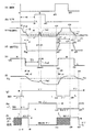
図3は図1、図2に示した第1、第2実施形態にかかるタイムチャートである。図3は図1及び図2に共通に適用される。 FIG. 3 is a time chart according to the first and second embodiments shown in FIGS. FIG. 3 is applied in common to FIGS.
図3(a)は上側入力信号HINを示す。上側入力信号HINは、上側ドライバUD及びインバータINV1を介してトランジスタM2,M3及びゲートコントロール回路7に印加される。
FIG. 3A shows the upper input signal HIN. The upper input signal HIN is applied to the transistors M2 and M3 and the
図3(b)は下側入力信号LINを示す。下側入力信号LINは下側ドライバLDを介してトランジスタPT2のゲートGに印加される。下側入力信号LINは、上側入力信号HINがローレベルLの時にたとえばハイレベルHとなるように設定される。なお、下側入力信号LINがローレベルLの時に上側入力信号HINもローレベルLに設定された期間が存在する。すなわち、両者の入力信号が共にローレベルLの期間を設けている。この期間がトランジスタPT1及びPT2が同時にオフとなるいわゆるデッドタイムである。 FIG. 3B shows the lower input signal LIN. The lower input signal LIN is applied to the gate G of the transistor PT2 through the lower driver LD. The lower input signal LIN is set to be at a high level H when the upper input signal HIN is at a low level L, for example. There is a period in which the upper input signal HIN is also set to the low level L when the lower input signal LIN is at the low level L. That is, both input signals have a low level L period. This period is a so-called dead time in which the transistors PT1 and PT2 are simultaneously turned off.
図3(c)はトランジスタPT1、すなわち上側パワートランジスタのゲートGに生じるゲート電圧Vhoを示す。ゲート電圧Vhoのふるまいは、上側入力信号HINに応動する。時刻t1で上側入力信号HINはターンオフする。すなわち、ハイレベルHからローレベルLに遷移するが、ゲート電圧Vhoのレベルは時刻t1から少し遅れた時刻t2から徐々に下がり始める。ゲート電圧Vhoのレベルはミラー期間と称される時刻t3〜t4でほぼ一定となる。ゲート電圧Vhoの大きさが一定になる電圧レベルが一般的にミラー電圧と称される。ミラー期間の時刻t4を過ぎるとゲート電圧Vhoは、時刻t5を経過すると閾値電圧Vthとなる時刻t6を経て出力時刻t7でほぼ0Vとなる。なお、時刻t5はゲート電圧Vhoがゲート電圧監視回路5に設定した監視電圧Vkに達する時刻を示す。時刻t6はゲート電圧VhoがトランジスタPT1のゲート閾値電圧Vthに達する時刻を示す。なお、時刻t4−t6までを時間τ1で示している。すなわち、時間τ1はトランジスタPT1のゲート電圧Vhoが監視電圧Vkに到達してからトランジスタPT1のゲート閾値電圧Vthに達するまでの比較的短い時間に相当する。時間τ1の期間ではトランジスタPT1はまだオン状態に置かれてはいるがオフに入る直前の状態である。
FIG. 3C shows the gate voltage Vho generated at the gate G of the transistor PT1, that is, the upper power transistor. The behavior of the gate voltage Vho is responsive to the upper input signal HIN. At time t1, the upper input signal HIN is turned off. That is, the transition from the high level H to the low level L is made, but the level of the gate voltage Vho starts to gradually decrease from time t2 slightly delayed from time t1. The level of the gate voltage Vho becomes substantially constant from time t3 to t4 called a mirror period. A voltage level at which the magnitude of the gate voltage Vho becomes constant is generally called a mirror voltage. After the time t4 of the mirror period, the gate voltage Vho becomes substantially 0 V at the output time t7 after the time t6 when the threshold voltage Vth is reached after the time t5. Time t5 indicates the time when the gate voltage Vho reaches the monitoring voltage Vk set in the gate
ゲート電圧Vhoは、時刻t7を過ぎると、時刻t10〜t11でスパイク状のノイズVn1が生じている状態を示している。このスパイク状のノイズVn1はゲート電圧Vhoに重畳されている状態を模式的に示したものであり、定常状態でのゲート電圧Vhoを示したものではない。ノイズ成分は、トランジスタPT2がオンするタイミング、すなわち、図3(b)に示した下側入力信号LINがハイレベルHとなる時刻t9から少し遅れた時刻t10〜t11の間に生じる状態を模式的に示している。時刻t9で下側入力信号LINがローレベルLからハイレベルHに切り替わると、信号に遅延がない場合、トランジスタPT2は時刻t9と同時にオン状態に入るはずである。しかし実際にオンしたのは時刻t9以降であり、トランジスタPT2のオンによって、監視電圧Vkを超えたノイズがトランジスタPT1のゲートに生じた時刻がt10〜t11であったことを示す。もし、信号の遅延時間を0とみなすと、時刻t10は時刻t9と同じとなる。トランジスタPT1のゲート電圧Vhoは時刻t11を過ぎると、上側入力信号HINがローレベルLからハイレベルHに遷移するタイミング、すなわち、上側入力信号HINがターンオンする時刻t13から少し遅れた時刻t14から徐々に上昇し。ゲート電圧VhoがトランジスタPT1の出力電流idが再び流れ始める時刻t15、ゲート電圧Vhoがゲート電圧監視回路5に設定した監視電圧Vkに達する時刻のt16、を経過したのち、ミラー期間の始まる時刻t17まで上昇する。上側入力信号HINが再びハイレベルHからローレベルに遷移するタイミングをt19とすると、時刻t19から少し遅れた時刻t20からゲート電圧Vhoが再び下がり始める。時刻t16から時刻t20までの時間をτ3で示す。
The gate voltage Vho shows a state in which spiked noise Vn1 occurs at time t10 to t11 after time t7. This spike-like noise Vn1 schematically shows a state of being superimposed on the gate voltage Vho, and does not show the gate voltage Vho in a steady state. The noise component is schematically shown at a timing when the transistor PT2 is turned on, that is, a state occurring between time t10 and time t11 slightly delayed from time t9 when the lower input signal LIN shown in FIG. It shows. When the lower input signal LIN switches from the low level L to the high level H at time t9, the transistor PT2 should enter the on state at the same time as time t9 if there is no delay in the signal. However, it was actually turned on after time t9, indicating that the time when noise exceeding the monitoring voltage Vk was generated at the gate of the transistor PT1 by the turning on of the transistor PT2 was from t10 to t11. If the delay time of the signal is regarded as 0, the time t10 is the same as the time t9. After the time t11, the gate voltage Vho of the transistor PT1 gradually changes from the timing when the upper input signal HIN transitions from the low level L to the high level H, that is, from the time t14 slightly delayed from the time t13 when the upper input signal HIN turns on. Rising. After the time t15 when the output voltage id of the transistor PT1 starts to flow again and the gate voltage Vho reaches the time t16 when the gate voltage Vho reaches the monitoring voltage Vk set in the gate
図3(d)はトランジスタPT1に流れる出力電流idを示す。出力電流idは、図3(c)に示したゲート電圧Vhoに応動する。出力電流idは、トランジスタPT1が深くオンしている期間、すなわちミラー期間の時刻t4までは最大値を維持しているが、ゲート電圧Vhoが低下するに応動して減少していく。ゲート電圧VhoがトランジスタPT1のゲート閾値電圧Vthを下回ると、トランジスタPT1はオフ状態に接近し最終的にはトランジスタPT1のゲート電圧Vhoが0Vになる時刻t7の近傍で出力電流idはほぼ0となる。 FIG. 3D shows the output current id flowing through the transistor PT1. The output current id responds to the gate voltage Vho shown in FIG. The output current id maintains the maximum value during the period when the transistor PT1 is deeply turned on, that is, until time t4 in the mirror period, but decreases in response to the decrease in the gate voltage Vho. When the gate voltage Vho falls below the gate threshold voltage Vth of the transistor PT1, the transistor PT1 approaches an off state, and finally, the output current id becomes almost 0 near the time t7 when the gate voltage Vho of the transistor PT1 becomes 0V. .
図3(e)はゲート電圧監視回路5の出力信号V5を示す。出力信号V5は、ゲート電圧Vhoがゲート電圧監視回路5に設定された監視電圧Vkよりも高い時にはハイレベルHとなり、低い時にはローレベルLとなる。したがって、時刻t1〜t5、t10〜t11、及びt16〜t22の期間ではハイレベルHとなり、時刻t5〜t10、t11〜t16、及び時刻t22以降はローレベルLとなる。なお、図3(e)に示す期間T1はゲート電圧監視回路5が動作し始める時刻t5からノイズ成分Vn2が生じる時刻t10までの時間、期間を表す。この期間は後述する信号遅延回路6を構成する積分回路が放電している期間でもある。
FIG. 3E shows the output signal V5 of the gate
図3(f)は信号遅延回路6からの出力信号V6を示す。出力信号V6は図3(e)に示した出力信号V5の立下りタイミングすなわち時刻t5から時刻t14に向かって緩やかに下降する。出力信号V6のレベルは信号遅延回路6を構成する積分回路の時定数に基づき、上側入力信号HINがハイレベルHに遷移するまでの間、緩やかに放電を続けるので低下していく。途中、ノイズVn3により時刻t10〜t11では出力信号V6は若干上昇するが、ノイズVn3のパルス幅は狭いので再び低下していく。
FIG. 3 (f) shows the
出力信号V6はゲートコントロール回路7に設定された閾値Vzを超えた後も緩やかに下降する。時刻t5から出力信号V6が閾値Vzに達する時刻t8までを時間τ2で示す。出力信号V6が閾値Vzを下回ると、ゲートコントロール回路7はトランジスタM4をオンさせる出力信号7を出力する。
The output signal V6 gradually falls after exceeding the threshold value Vz set in the
時間τ2は図3(c)で説明した時間τ1よりも大きくなるように、すなわち、τ2>τ1となるように信号遅延回路6の回路定数が決められている。こうした条件設定によって、トランジスタM4がオフからオンに遷移するタイミングをトランジスタPT1の出力電流idが0になった後に行うことができる。すなわち、トランジスタPT1のオフ時のゲート抵抗をハイレベルH(トランジスタM3のオン抵抗)からローレベルL(トランジスタM3,M4の並列オン抵抗)への切替えをトランジスタPT1の出力電流idが0になった後に実行することができる。こうしたことはトランジスタPT1のdi/dt値を小さくできるので、ワイヤーLWのインダクタンス成分lw等によって生じる過渡電圧Δvを小さく抑え、トランジスタM2,M3の耐圧劣化を抑止することができる。
The circuit constants of the
図3(f)に示した時間τ2と図3(c)に示した時間τ1との大小関係は先に述べたとおりであるが、時間τ2と時間T1との間にはτ2<T1なる条件を満たすようにも設定されている。時間T1は時刻t5から時刻t10までの時間である。すなわち、T1=t10−t5として表すことができる。時刻t10はノイズ成分Vnが発生すると仮定した時刻である。しかし、ノイズ成分Vn1〜Vn3は、図3(b)に示した下側入力信号LINがローレベルLからハイレベルHに遷移する時刻t9〜t12の期間内に生じうる。したがって、ノイズ成分Vn1〜vn3が時刻t9で発生した時でも信号遅延回路6はゲート電圧監視回路5から入力された出力信号V5に含まれているノイズ成分Vn1〜Vn3を十分に抑圧、減衰させ、信号遅延回路6から出力される出力信号V6に含まれるノイズ成分Vn3が閾値Vzを下回るように信号遅延回路6の回路定数を設定しなければならない。こうした条件を満足させるならば、下側入力信号LINによってトランジスタPT2がオフからオンするときの、いわゆるターンオン時にトランジスタPT2のdV/dt(電圧の時間変化率)によってトランジスタPT1のゲート電圧過度の上昇を抑えし、トランジスタPT1がセルフターンオンするという不具合を排除することができる。出力信号V6は図3(e)に示した出力信号V5の立上りタイミングすなわち時刻t16から時刻t22に向かって緩やかに上昇する。時刻t16から出力信号V6が閾値Vzに達する時刻t18までの時間をτ4で示している。なお、出力信号V6のレベルが閾値Vzと同じなる時刻は時刻t18ではなく、時刻t18よりも早い時刻t16〜t17の間でも構わない。
The magnitude relationship between the time τ2 shown in FIG. 3 (f) and the time τ1 shown in FIG. 3 (c) is as described above, but the condition that τ2 <T1 exists between the time τ2 and the time T1. It is also set to satisfy. Time T1 is the time from time t5 to time t10. That is, it can be expressed as T1 = t10−t5. Time t10 is a time when it is assumed that the noise component Vn is generated. However, the noise components Vn1 to Vn3 can occur within the period from time t9 to t12 when the lower input signal LIN shown in FIG. 3B transitions from the low level L to the high level H. Therefore, even when the noise components Vn1 to vn3 are generated at time t9, the
時間τ4は図3(e)に示した時間τ3より小さくなるように、すなわち、τ3>τ4となるように遅延回路6の回路定数が決められている。すなわち、トランジスタPT1のゲート電圧Vhoと監視電圧Vkとが一致した時刻t16からトランジスタPT1がターンオフを開始する時刻t20までの時間をτ3とし、トランジスタPT1のゲート電圧Vhoと監視電圧Vkとが一致する時刻t16から、ゲートコントロール回路7に設定された閾値電圧Vzと信号遅延回路6の出力信号V6のレベルが一致する時刻t18までの時間をτ4としたとき、τ3>τ4になるように設定されている。こうした条件設定によって、トランジスタPT1がオフに遷移する時、トランジスタM4がオフする、すなわち、トランジスタPT1のゲート抵抗をハイレベルHに維持することである。こうしたことは、前記のように、トランジスタPT1のdi/dt値を小さくできるので、ワイヤーLWのインダクタンス成分lw等によって生じる過渡電圧Δvを小さく抑え、トランジスタM2,M3の耐圧劣化を抑止することができる。
The circuit constant of the
図3(g)は、トランジスタM3のオン、オフ状態を示すと共にトランジスタM3のゲート電圧も示している。トランジスタM3のゲート電圧は、上側入力信号HINの極性が反転されたものにほぼ等しい。時刻t1から少し遅れた時刻t2でローレベルLからハイレベルHに遷移し、時刻t13から少し遅れた時刻t14でハイレベルHからローレベルLに遷移する。トランジスタM3は、時刻t2〜t14の期間オンとなる。 FIG. 3G shows the on / off state of the transistor M3 and also shows the gate voltage of the transistor M3. The gate voltage of the transistor M3 is substantially equal to that obtained by inverting the polarity of the upper input signal HIN. The transition from the low level L to the high level H at time t2 slightly delayed from the time t1, and the transition from the high level H to low level L at the time t14 slightly delayed from the time t13. The transistor M3 is on during the period from time t2 to time t14.
図3(h)は、ゲートコントロール回路7の出力信号V7を示す。出力信号V7はトランジスタM4のゲートGに印加される。出力信号7はトランジスタM3のゲートGに印加された電圧Vhbと信号遅延回路6から出力された出力信号V6とが論理積演算された演算結果である。出力信号V7は、時刻t1〜t8でローレベルLを時刻t8〜t14ではハイレベルHをそれぞれ示し、時刻t14〜t25は再びローレベルLを示す。出力信号V7がハイレベルHの時トランジスタM4はオンし、ローレベルの時オフする。上側入力信号HINがターンオンする時刻t13から少し遅れた時刻t14で、ゲートコントロール回路7を構成する論理積回路73の第1端にはノードHBの信号が入力されため、信号遅延回路6の出力V6に関わらず、論理積回路73がローレベルLを出力する。すなわち、トランジスタM4とトランジスタM3がほぼ同じ時刻でターンオフすることが保障できるので、トランジスタM4とトランジスタM2の同時オンが避けられる。
FIG. 3 (h) shows the
図3(i)は、トランジスタPT1のゲート抵抗を示す。ここでゲート抵抗はトランジスタPT1のゲートGとソースSとの間に介在される抵抗である。ゲート抵抗はトランジスタM3がオンでトランジスタM4がオフのときにはトランジスタM3のオン抵抗がゲート抵抗となるために相対的に高く(H)なり、トランジスタM3及びトランジスタM4が共にオンであるトランジスタM3及びM4の並列抵抗がゲート抵抗となるので相対的にトランジスタPT1のゲート抵抗は低く(L)となる。トランジスタPT1のゲート抵抗はトランジスタPT2がオンである時ローレベルLに維持される。なお、トランジスタM3及びM4が共にオフである期間xにおいては、トランジスタM2のみがオンとなりトランジスタPT1のオフ時のゲート抵抗はハイインピーダンスとなる。 FIG. 3I shows the gate resistance of the transistor PT1. Here, the gate resistance is a resistance interposed between the gate G and the source S of the transistor PT1. When the transistor M3 is on and the transistor M4 is off, the gate resistance is relatively high (H) because the on-resistance of the transistor M3 is the gate resistance, and the transistors M3 and M4 in which both the transistors M3 and M4 are on are turned on. Since the parallel resistance becomes the gate resistance, the gate resistance of the transistor PT1 is relatively low (L). The gate resistance of the transistor PT1 is maintained at a low level L when the transistor PT2 is on. In the period x in which both the transistors M3 and M4 are off, only the transistor M2 is on and the gate resistance when the transistor PT1 is off is high impedance.
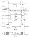
図4は本発明の第2実施形態(図2)で、信号遅延回路6の回路定数の設定が適切に行われなかった場合のタイムチャートを示す。
FIG. 4 shows a time chart when the circuit constant of the
図4(a),(b),(c),(d),(e),及び(g)は既に説明した図3(a),(b),(c),(d),(e),及び(g)とそれぞれほぼ同じであるので説明は省略する。 4 (a), (b), (c), (d), (e), and (g) are already described with reference to FIGS. 3 (a), (b), (c), (d), (e). ) And (g) are substantially the same, and the description thereof is omitted.
図4(f)は信号遅延回路6から出力される出力信号V6を示す。出力信号V6は信号遅延回路6の回路定数の設定が不適切であったためノイズ成分vn3がゲートコントロール回路7の閾値Vzよりも依然としてレベルが高い状態に存在することを模式的に示している。また、遅延回路6の出力信号V6の電圧値がゲート電圧監視回路5の出力V5がハイレベルHの時間t16からt22まで徐々に上昇する。時刻t22では、信号遅延回路6の出力信号V6の昇圧がまだ終わらない場合、時刻t22から出力信号V6が閾値Vzに達する時刻t25aまでの遅延時間が短くなり、図4(c)に示したようにトランジスタPT1のdi/dt(電流の時間変化率)値が大きくなる可能性がある。di/dt値が大きくなることはトランジスタM2,M3の耐圧からみて避けたいところである。
FIG. 4 (f) shows an
図4(h)はゲートコントロール回路7から出力される出力信号V7を示す。出力信号V7は本来時刻t10a〜t11aの期間においてもハイレベルHであるべきであるが図4(f)に示したノイズ成分Vn3が閾値Vzよりも高いために時刻t10a〜t11aの期間ローレベルLになった状態を示す。
FIG. 4H shows the output signal V7 output from the
図4(i)はトランジスタPT1のゲート抵抗の大きさを模式的に示す。ゲート抵抗はゲート電圧監視回路5、信号遅延回路6、及びゲートコントロール回路7が正規に動いている時は時刻10a〜11aの期間でもローレベルLであるはずである。しかし、信号遅延回路6の回路定数の設定が不適切であるため、時刻10a〜11aの期間、トランジスタM4はオフに置かれる。このため、トランジスタPT1のゲート抵抗の切替えが実行されなかった状態を示す。
FIG. 4I schematically shows the magnitude of the gate resistance of the transistor PT1. When the gate
以上、本発明に採用したゲート電圧監視回路5、信号遅延回路6、ゲートコントロール回路7、及びトランジスタM4を採用した回路構成によって、トランジスタPT1のオフ時のゲート抵抗を切り替え、電力損失の低減化及びゲートドライバ、すなわちトランジスタM2,M3の耐圧を保障するのに好適である。しかし、上記したように、特に信号遅延回路6の回路定数の設定が不適切の場合には本来の効果は低減するので留意しなければならない。
As described above, the gate
(第3実施形態)
図5は本発明にかかる第3実施形態を示す。図5は、上記した図2(第2実施形態)で示す構成において、ゲート電圧監視回路5、及びゲートコントロール回路7をさらに詳細に示したものである。なお、図1及び図2と同じ箇所には同じ符号を付与し、説明を省略する。
(Third embodiment)
FIG. 5 shows a third embodiment according to the present invention. FIG. 5 shows the gate
本発明にかかる第3実施形態においても、ゲート電圧監視回路5には監視電圧Vkが設定され、その監視電圧Vkは上記のとおりトランジスタPT1のミラー電圧Vm以下に設定される。ゲート電圧監視回路5はトランジスタPT1のゲートG及び外部端子KILLにそれぞれに接続され、トランジスタPT1のゲートGからのゲート電圧Vhoと外部端子KILLに印加されるキラー信号Kiとの論理積演算結果を出力信号V5として出力する。出力信号V5は信号遅延回路6に入力される。
Also in the third embodiment according to the present invention, the monitoring voltage Vk is set in the gate
ゲート電圧監視回路5は、インバータINV51,INV52及び否定論理積回路NA53を備える。インバータINV51の入力はトランジスタPT1のゲートG、すなわち、ノードHOに接続され、インバータINV51の出力は否定論理積回路NAの第1端に接続される。インバータINV51はたとえばCMOSインバータで構成され、インバータINV51のスイッチング特性に基づき監視電圧Vkが設定されている。トランジスタPT1のゲート電圧VhoがインバータINV51を介して否定論理積回路NAの第1端に印加される。インバータINV52の入力は外部端子KILLに接続される。外部端子KILLにはキラー信号Kiが印加される。キラー信号KiはハイレベルHまたはローレベルLに設定される。本発明の一実施形態ではキラー信号KiがローレベルLのときにゲート電圧監視回路5は正規に働き、ゲート電圧監視回路5の後段に結合される信号遅延回路6及びゲートコントロール回路7も正規に働く。キラー信号KiがハイレベルHに設定されると、ゲート電圧監視回路5の回路動作は遮断、停止する。この時には後段の信号遅延回路6及びゲートコントロール回路7も遮断、停止される。
The gate
ゲート電圧監視回路5、信号遅延回路6及びゲートコントロール回路7の回路動作の効果は、キラー信号KiをローレベルL及びハイレベルHに設定した時の出力端子として用意した外部端子OUTの出力信号波形、出力電流波形を比較すれば判定することができる。
The effect of the circuit operation of the gate
図5に示した信号遅延回路6は第2実施形態(図2)と同じ抵抗R63及びキャパシタC64で構成している。抵抗R63及びキャパシタC64は積分回路、すなわちローパスフィルタで構成される。こうしたローパスフィルタは1段だけではなく複数段で構成してもかまわない。信号遅延回路6は出力信号V5に含まれるノイズ成分Vn1,Vn2を抑圧、除去するための効果を果たす。
The
ゲートコントロール回路7は第2実施形態(図2)と異なり、NMOSトランジスタM71、PMOSトランジスタM72、論理積回路73、及びインバータINV74で構成される。
Unlike the second embodiment (FIG. 2), the
ゲートコントロール回路7においては、トランジスタM71とM72とがノードN7を介して直列に接続される。トランジスタM72のゲートGはノードHB及び論理積回路73の第1端に接続される。トランジスタM72のドレインDは論理積回路73の第2端及びトランジスタM71のドレインDに接続されると共に、ノードN7に接続される。ノードN7にはインバータINV74の入力が接続され、インバータINV74の出力は、トランジスタPT1のゲート抵抗を切り替えるために用意したトランジスタM4のゲートに接続される。インバータINV74はたとえばCMOSインバータで構成され、該CMOSインバータのスイッチング特性に基づき、閾値電圧Vzが設定されている。論理積回路73の出力はトランジスタM71のゲートGに接続される。ノードN7は信号遅延回路6の出力、すなわち、抵抗63とキャパシタC64との共通接続点に接続される。トランジスタM72とトランジスタM71とはブート端子としての外部端子VBと出力端子としての外部端子OUTとの間に直列に接続されたCMOSインバータであり、ノードN7は該CMOSインバータの出力端とみることができる。したがって、出力信号V6が出力される信号遅延回路6の出力信号は該CMOSインバータの出力と信号遅延回路6の出力が加算されたものとなる。言い換えれば出力信号V6は該CMOSインバータによって制御される。
In
図6は第3実施形態のタイムチャート図である。図6は図3と類似しているが、実質的には第1に図6(f)の電圧波形が図3(f)とは相違すること。第2に図6(g)にトランジスタM71のオン、オフ状態を示したこと。第3に図6(h)にトランジスタM72のオン、オフ状態を示していることである。なお、図6は図5に示したキラー端子としての外部端子KILLをローレベルLに設定し、ゲート電圧監視回路5、信号遅延回路6、及びゲートコントロール回路7を正規の状態で動作させたときのものである。
FIG. 6 is a time chart of the third embodiment. FIG. 6 is similar to FIG. 3, but first, the voltage waveform of FIG. 6 (f) is substantially different from FIG. 3 (f). Second, FIG. 6G shows the on / off state of the transistor M71. Third, FIG. 6H shows the on / off state of the transistor M72. 6 shows the case where the external terminal KILL as the killer terminal shown in FIG. 5 is set to the low level L, and the gate
図6の大部分は既に述べた図3と同じであるので同じ箇所についての説明は省略する。ここでは図6(f),(g)及び(h)について説明する。 Since most of FIG. 6 is the same as FIG. 3 already described, description of the same part is omitted. Here, FIGS. 6F, 6G, and 6H will be described.
図6(f)はノイズフィルタ6から出力される出力信号V6を示す。出力信号V6は時刻t8で急峻にローレベルLとなり、このローレベルLは時刻t14まで続く。こうした特性は図3(f)に示した時刻t8〜t14での特性とは大きく異なる。これは、時刻t8〜t14の間の特性は、図5に示したトランジスタM71とトランジスタM72で構成したCMOSインバータの特性で決定されてからである。前述の通り、時刻t8で遅延回路6の出力V6がゲートコントロール回路7の閾値Vzに達し、論理積回路73の出力信号のハイレベルHがトランジスタM71のゲートGに印加し、トランジスタM71がオンになる。その時、遅延回路6のキャパシタC64がショットになり、遅延回路6の出力信号V6が急峻にローレベルLとなる。すなわち、t8時刻で前記CMOSインバータを用いて、トランジスタPT1のオフ時のゲート抵抗の切り替えを遅延回路6の特性と切り離して行うようにしている。
FIG. 6 (f) shows an
上側入力信号HINがターンオンする時刻t13から少し遅れた時刻t14では、前記CMOSインバータのトランジスタM72がオン、トランジスタM71がオフの状態になるため、トランジスタM71両端の電位差が直接キャパシタC64両端にかけられる。キャパシタC64が迅速に充電され、遅延回路6の出力電位V6が急峻にハイレベルHになるので、前記τ3>τ4の条件が不要となる。
At a time t14 slightly delayed from the time t13 when the upper input signal HIN is turned on, the transistor M72 of the CMOS inverter is turned on and the transistor M71 is turned off, so that the potential difference across the transistor M71 is directly applied across the capacitor C64. Since the capacitor C64 is quickly charged and the output potential V6 of the
図6(g)はトランジスタM71のオン、オフ状態を示す。トランジスタM71のオン期間は時刻t8〜t14となる。出力信号V6のローレベルLの期間とトランジスタM71のオン期間はほぼ同じである。 FIG. 6G shows the on / off state of the transistor M71. The on period of the transistor M71 is from time t8 to t14. The low level L period of the output signal V6 and the ON period of the transistor M71 are substantially the same.
図6(h)はトランジスタM72のオン、オフ状態を示す。トランジスタM72のオン、オフは上側入力信号HINのハイレベルH及びローレベルLに応動する。すなわち、上側入力信号HINがハイレベルHの時、トランジスタM72はオンであり、上側入力信号HINがローレベルLの時オフとなる。 FIG. 6H shows the on / off state of the transistor M72. The transistor M72 is turned on / off in response to the high level H and the low level L of the upper input signal HIN. That is, when the upper input signal HIN is at the high level H, the transistor M72 is turned on, and when the upper input signal HIN is at the low level L, it is turned off.
図7は図5に示した第3実施形態において、外部端子KILLをハイレベルHに設定し、ゲート電圧監視回路5、信号遅延回路6、及びゲートコントロール回路7の動作を遮断、停止させてトランジスタM4をオフにしてトランジスタPT1のゲート抵抗の大きさの違いによる効果の程度を確認する時のタイムチャートを示す。
FIG. 7 shows the third embodiment shown in FIG. 5, in which the external terminal KILL is set to a high level H, and the operations of the gate
図7(a)は上側入力信号HINを示す。上側入力信号HINは時刻t1でハイレベルHからローレベルLに遷移する状態を示している。 FIG. 7A shows the upper input signal HIN. The upper input signal HIN shows a state of transition from the high level H to the low level L at time t1.
図7(b)は外部端子KILLに印加するキラー信号Kiを示す。キラー信号Kiは時刻t1よりも早い時刻t0でローレベルLからハイレベルHに遷移するように設定されている。本発明の一実施の形態ではキラー信号KiがローレベルLのときには本発明にかかるトランジスタPT1のゲート抵抗の大きさを確認するチェック機能は遮断され、キラー信号KiがハイレベルHのときにチェック機能が実行される。このため、チェック機能を実行するときには、キラー信号Kiの切替えが他の信号、電圧の切替わりよりも優先させている。もしキラー信号KiのローレベルLからハイレベルHの切替えが時刻t1よりも遅くなると本発明の十分な効果は期待できないことになる。 FIG. 7B shows a killer signal Ki applied to the external terminal KILL. The killer signal Ki is set to transition from the low level L to the high level H at time t0 earlier than time t1. In one embodiment of the present invention, when the killer signal Ki is at a low level L, the check function for checking the magnitude of the gate resistance of the transistor PT1 according to the present invention is cut off, and when the killer signal Ki is at a high level H, the check function Is executed. For this reason, when executing the check function, switching of the killer signal Ki is given priority over switching of other signals and voltages. If the switching of the killer signal Ki from the low level L to the high level H becomes later than the time t1, the sufficient effect of the present invention cannot be expected.
キラー信号Kiが時刻t0でレベルがローレベルLからハイレベルHに切替えられると、時刻t1以降、ゲート電圧監視回路5、信号遅延回路6、及びゲートコントロール回路7は正規の動作状態から切り離され遮断、停止する。
When the level of the killer signal Ki is switched from the low level L to the high level H at time t0, the gate
図7(c)はトランジスタM2のオン、オフ状態を示す。トランジスタM2は図7(a)に示した上側入力信号HINに応動する。上側入力信号HINがハイレベルH及びローレベルLであるとき、トランジスタM2はそれぞれオン及びオフとなる。 FIG. 7C shows the on / off state of the transistor M2. The transistor M2 responds to the upper input signal HIN shown in FIG. When the upper input signal HIN is at the high level H and the low level L, the transistor M2 is turned on and off, respectively.
図7(d)はトランジスタM3のオン、オフ状態を示す。トランジスタM3は図7(a)に示した上側入力信号HINに応動する。上側入力信号HINがハイレベルH及びローレベルLであるとき、トランジスタM3はそれぞれオフ及びオンとなる。トランジスタM3のオン、オフ状態は図7(c)に示したトランジスタM2のそれとは回路構成上及びトランジスタの導電形式の違いから相補的な関係に置かれる。したがって、トランジスタM2がオフのとき、トランジスタM3はオンであり、トランジスタM2がオンのとき、トランジスタM3はオフとなる。 FIG. 7D shows the on / off state of the transistor M3. The transistor M3 responds to the upper input signal HIN shown in FIG. When the upper input signal HIN is at the high level H and the low level L, the transistor M3 is turned off and on, respectively. The on / off state of the transistor M3 is in a complementary relationship with that of the transistor M2 shown in FIG. 7C in terms of the circuit configuration and the difference in the conductivity type of the transistor. Therefore, the transistor M3 is on when the transistor M2 is off, and the transistor M3 is off when the transistor M2 is on.
図7(e)はトランジスタPT1のゲート電圧Vho、すなわちノードHOの電圧を示す。ゲート電圧Vhoは、図7(b)に示したキラー信号Kiの影響を受けずにトランジスタM2のオン、オフに応動する。すでに説明した図3及び図6にも示したようにゲート電圧Vhoは、時刻t2から時刻t3に向かって徐々に下降し、時刻t3〜t4のミラー期間でほぼ一定のミラー電圧Vmに維持され、ミラー期間を過ぎると時刻t7に向かってさらに下降し始める。 FIG. 7E shows the gate voltage Vho of the transistor PT1, that is, the voltage at the node HO. The gate voltage Vho responds to on / off of the transistor M2 without being affected by the killer signal Ki shown in FIG. As shown in FIGS. 3 and 6 already described, the gate voltage Vho gradually decreases from time t2 to time t3, and is maintained at a substantially constant mirror voltage Vm in the mirror period from time t3 to t4. After passing the mirror period, it starts to descend further toward time t7.
図7(f)はゲート電圧監視回路5の出力信号V5を示す。ゲート電圧監視回路5は、キラー信号Kiに回路動作が時刻t0以降は遮断、停止されているのでローレベルLとなる。なお、時刻t0以前はキラー信号KiがローレベルLであり、ゲート電圧監視回路5は正規の動作状態に置かれるが、トランジスタPT1,PT2が共にオフであるデッドタイム期間であるのでローレベルLとなる。
FIG. 7 (f) shows the
図7(g)は信号遅延回路6の出力信号V6を示す。信号遅延回路6には前段のゲート電圧監視回路5からの信号が存在しないため出力信号V5と同様にローレベルLとなる。
FIG. 7G shows the
図7(h)はゲートコントロール7の出力信号V7を示す。出力信号V7はトランジスタM4のゲートGに印加される信号でもある。出力信号V7は信号遅延回路6から出力される出力信号V6に基づき生成されるものであるから出力信号V6と同様にローレベルLとなる。この時、トランジスタM4はオフ状態に置かれる。
FIG. 7 (h) shows the
図7(i)はゲートコントロール回路7を構成するトランジスタM71のオン、オフ状態を示す。トランジスタM71のオン、オフは論理積回路73の出力信号で行われる。トランジスタM71はNMOSトランジスタであるので、トランジスタM71のオン、オフはそのゲートGに印加されるゲート電圧に対応する。すなわち、トランジスタM71のゲート電圧がハイレベルHのときトランジスタM71はオンとなり、ローレベルLのときトランジスタM71はオフとなる。
FIG. 7I shows the on / off state of the transistor M71 constituting the
図7(j)はトランジスタM72のオン、オフ状態を示す。トランジスタM72のゲートGには上側入力信号HINの反転信号HINBが印加される。このため、トランジスタM72のオン、オフ状態は図7(a)に示した上側入力信号HINに応動する。すなわち、上側入力信号HINがハイレベルH及びローレベルLのとき、トランジスタM72はそれぞれオン及びオフとなる。 FIG. 7J shows the on / off state of the transistor M72. An inverted signal HINB of the upper input signal HIN is applied to the gate G of the transistor M72. For this reason, the ON / OFF state of the transistor M72 responds to the upper input signal HIN shown in FIG. That is, when the upper input signal HIN is at the high level H and the low level L, the transistor M72 is turned on and off, respectively.
図7(k)はトランジスタPT1のゲート抵抗がハイレベルHであるかローレベルLであるかを示す。トランジスタM3がオンであり、トランジスタM4がオフであるときにトランジスタPT1のゲート抵抗は、トランジスタM3のオン抵抗にほぼ等しくなり、イレベルHとなる。トランジスタM3,M4が共にオンであるときトランジスタPT1のゲート抵抗はローレベルLとなる。しかし、図7はキラー信号Kiによって、ゲート電圧監視回路5、信号遅延回路6、及びゲートコントロール回路7の回路動作が遮断、停止された時を示しているのでトランジスタPT1のゲート抵抗がローレベルLに固定される期間は存在しない。なお、斜線で示した期間xは、トランジスタPT1,PT2のデッドタイム及びキラー信号Kiが印加される期間であるのでトランジスタPT1のオフ時のゲート抵抗はハイインピーダンスとなる。
FIG. 7 (k) shows whether the gate resistance of the transistor PT1 is high level H or low level L. When the transistor M3 is on and the transistor M4 is off, the gate resistance of the transistor PT1 is substantially equal to the on-resistance of the transistor M3, and becomes the low level H. When both the transistors M3 and M4 are on, the gate resistance of the transistor PT1 is at a low level L. However, FIG. 7 shows a case where the circuit operations of the gate
図8は第3実施形態(図5)に用いたゲートコントロール回路7の変形例を示す。図8に示したゲートコントロール回路7が図5に示したそれと大きく相違するのは、ノードN7とインバータ74の入力端との間にシュミットトリガSHを接続したことである。
FIG. 8 shows a modification of the
シュミットトリガは、一般的に入力信号に対して閾値を2つ有し、入力信号に含まれるノイズ成分によって起こる誤動作を排除するものとして広く使用されている。図8に示したシュミットトリガSHは、トランジスタM701,M702,M703,M704,M705及びM706で構成される。トランジスタM701,M705は導電形式がPMOSからなり、トランジスタM702,M703,M704及びM706は導電形式がNMOSである。 A Schmitt trigger generally has two thresholds for an input signal, and is widely used to eliminate malfunctions caused by noise components included in the input signal. The Schmitt trigger SH shown in FIG. 8 includes transistors M701, M702, M703, M704, M705, and M706. The transistors M701 and M705 have a conductivity type of PMOS, and the transistors M702, M703, M704, and M706 have a conductivity type of NMOS.
トランジスタM701のソースSは電源端子VCに接続される。トランジスタM701及びトランジスタM702のドレインD同士は共通接続され、その共通接続点はノードN71で示される。トランジスタM701,M702のゲートG同士は共通接続され、その共通ゲートはノードN7に接続される。ノードN7には信号遅延回路6から出力された出力信号V6が印加される。トランジスタM702のソースSはトランジスタM703のドレインDに接続される。トランジスタM703のドレインDとトランジスタM702のソースSとの共通接続点はノードN72で示される。トランジスタM703のソースSは接地電位GNDに接続され、そのゲートGはトランジスタM702のゲートGと共通接続される。
The source S of the transistor M701 is connected to the power supply terminal VC. The drains D of the transistors M701 and M702 are connected in common, and the common connection point is indicated by a node N71. The gates G of the transistors M701 and M702 are connected in common, and the common gate is connected to the node N7. The output signal V6 output from the
トランジスタM701,M702のドレインD同士が共通接続されたノードN71にはトランジスタM705,M706のゲートGが共通に接続される。トランジスタM705のソースSは第1電源端子としての外部端子VCに接続され、そのドレインDはトランジスタM706のドレインDに接続される。トランジスタM705,M706のドレインD同士の共通接続点はノードN73で示す。トランジスタM706のソースSは接地電位GNDに接続される。トランジスタM705とトランジスタM706とでCMOSインバータを構成している。 The gates G of the transistors M705 and M706 are commonly connected to a node N71 where the drains D of the transistors M701 and M702 are commonly connected. The source S of the transistor M705 is connected to the external terminal VC as the first power supply terminal, and the drain D thereof is connected to the drain D of the transistor M706. A common connection point between the drains D of the transistors M705 and M706 is indicated by a node N73. The source S of the transistor M706 is connected to the ground potential GND. The transistor M705 and the transistor M706 constitute a CMOS inverter.
ノードN73にはトランジスタM704のゲートGが接続される。トランジスタM701,M702,M703及びM704のそれぞれのオン抵抗に基づきシュミットトリガSHの2つの閾値が設定されている。トランジスタM701,M702,M703及びM704のそれぞれのオン抵抗は、それぞれのトランジスタのチャネル幅、チャネル長を適宜設定されることで決定することができる。 The gate G of the transistor M704 is connected to the node N73. Two threshold values of the Schmitt trigger SH are set based on the respective on-resistances of the transistors M701, M702, M703, and M704. The on-resistances of the transistors M701, M702, M703, and M704 can be determined by appropriately setting the channel width and channel length of each transistor.
また、ノードN73にはインバータINV74の入力が接続され、インバータINV74の出力はゲートコントロール回路7の出力信号V7としてトランジスタM4のゲートGに印加される。
The node N73 is connected to the input of the inverter INV74, and the output of the inverter INV74 is applied to the gate G of the transistor M4 as the output signal V7 of the
なお、図8に示したシュミットトリガSHはゲートコントロール回路7に採用したが、これと同様のものをゲート電圧監視回路5に用いることもできる。
Although the Schmitt trigger SH shown in FIG. 8 is adopted in the
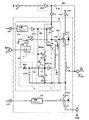
図9は、本発明及び従来技術に適用されるパワーモジュール回路装置(IPM)100Aを示す回路図である。パワーモジュール回路装置100Aは上側ドライバ20を含む。なお、上側ドライバ20は図1、図2、図5に示した本発明にかかるパワー半導体駆動回路10を含む。さらに、パワーモジュール回路装置100AはRSフリップフロップ回路21、減電圧保護回路22、抵抗23,24、NMOSトランジスタ25,26、パルス発生回路27、レベルシフタ28、ブート電流制御回路29、シュミットトリガ30、下側ドライバ31、論理制御回路32、信号遅延回路33、レベルシフタ34、シュミットトリガ35、NMOSトランジスタ36、異常信号生成回路37、熱保護回路38、減電圧保護回路39、コンパレータ40、標準電圧生成回路41を含む。なお、図9に示したパワーモジュール回路にはキラー信号Kiを印加する外部端子KILLは示していない。
FIG. 9 is a circuit diagram showing a power module circuit device (IPM) 100A applied to the present invention and the prior art. The power
図9に示すパワーモジュール回路装置100Aは、さらにキャパシタCB及びダイオードDBを含む。キャパシタCB及びダイオードDBによってブートストラップ回路を構成する。キャパシタCBとダイオードDBとの共通接続点に生じたブート電圧VBBは外部端子VBを介して上側ドライバ20等を駆動するための電源電圧として利用される。なお、パワーモジュール回路装置100AはDIPに実装されている。
Power
図10は図5に示した本発明にかかるパワー半導体駆動回路10と、図11に示した従来のパワー半導体駆動回路10を図9に示したパワーモジュール回路装置100A(IPM)に用いたときの駆動損失を比較した結果である。ここで、駆動損失とは、入力電力から出力電力を引いた電力を指す。たとえば、入力電力が1[W]である場合、出力電力が0.9[W]であった場合の駆動損失は1−0.9=0.1[W]となる。図10で横軸は、従来と本発明を対比させ、トランジスタPT1に流れる出力電流idの実効値(rms)がそれぞれ1[A]、2[A]及び4[A]の時の従来と本発明をそれぞれ示す。縦軸は駆動損失を正規化した数値で表している。ここでは、従来の駆動損失を1.00とした時の本発明での駆動損失を数値で示している。駆動損失の数値が小さい程、入力電力に対する出力電力が大きいことを示す。すなわち電力効率が高いことを表す。駆動損失は電源電圧や出力電流、駆動信号の周波数、制御方式などで異なってくる。今回の比較では、第2電源端子である外部端子Pの電圧VPPは400V、第1電源端子としての外部端子VCの電圧VCCは15V、周波数は5kHz、PWMの3位相変調方式としている。
FIG. 10 shows a case where the power
出力電流idの実効値が1[Arms]、2[Arms]、及び4[Arms]の時のそれぞれの本発明での駆動損失は、それぞれ0.70、0.74、及び0.79であった。出力電流idが増加するにつれ、駆動損失の比率は大きくなり、駆動損失の低減効果は少し低下するがが、それでも本発明では従来のものに比べて20%以上の電力消費を低減できることがわかった。 When the effective value of the output current id is 1 [Arms], 2 [Arms], and 4 [Arms], the drive loss in the present invention is 0.70, 0.74, and 0.79, respectively. It was. As the output current id increases, the ratio of driving loss increases and the effect of reducing driving loss is slightly reduced. However, it has been found that the present invention can reduce power consumption by 20% or more compared to the conventional one. .
本発明の構成は、上記実施の形態のほか、発明の主旨を逸脱しない範囲で様々の変更を加えることが可能である。即ち、上記実施の形態は、全ての点で例示であって、制限的なものでないと考えられるべきであり、本発明の技術的範囲は、上記実施形態の説明ではなく、特許請求の範囲によって示されるものであり、特許請求の範囲と均等の意味及び範囲内に属する全ての変更が含まれると理解されるべきである。 The configuration of the present invention can be variously modified in addition to the above-described embodiment without departing from the spirit of the invention. That is, the above-described embodiment is an example in all respects and should not be considered as limiting, and the technical scope of the present invention is not the description of the above-described embodiment, but the claims. It should be understood that all modifications that come within the meaning and range of equivalents of the claims are included.
以上説明したように、本発明のパワー半導体駆動回路、パワー半導体回路、及びパワーモジュール回路装置は、高電圧大電流での高速スイッチング化に伴い、特にオン状態からオフ状態時のインダクタンス成分によるゲートドライバ耐圧破壊を防ぎ、且つパワー半導体素子のオン、オフ時でのセルフターンオンを防ぎ、スイッチング損失の増加を抑止することができるので、その産業上の利用可能性は極めて高い。 As described above, the power semiconductor drive circuit, the power semiconductor circuit, and the power module circuit device according to the present invention have a high-speed switching with a high voltage and a large current, and in particular, a gate driver based on an inductance component in an on state to an off state. Since it is possible to prevent breakdown withstand voltage, prevent self-turn-on when the power semiconductor element is turned on and off, and suppress an increase in switching loss, the industrial applicability is extremely high.
5 ゲート電圧監視回路
6 信号遅延回路
7 ゲートコントロール回路
10 パワー半導体駆動回路
10A パワー半導体回路
20 上側ドライバ
21 RSフリップフロップ回路
22 減電圧保護回路
23,24 抵抗
25,26 NMOSトランジスタ
27 パルス発生回路
28 レベルシフタ
29 ブート電流制御回路
30 シュミットトリガ
31 下側ドライバ
32 論理制御回路
33 遅延回路
34 レベルシフタ
35 シュミットトリガ
36 NMOSトランジスタ
37 異常信号生成回路
38 熱保護回路
39 減電圧保護回路
40 コンパレータ
41 標準電圧生成回路
73 論理積回路
100 パワーモジュール回路装置
BS ブートストラップ回路
C64 キャパシタ(積分回路)
CB キャパシタ(ブートストラップキャパシタ)
DB ダイオード(ブートストラップダイオード)
GND 接地電位
HO ノード
HB ノード
HIN 上側入力信号(駆動信号)
id 出力電流(トランジスタPT1のソース・ドレイン間電流)
INV1,INV51,INV52,INV74,INV732,INV733 インバータ
KILL 外部端子(キラー端子)
Ki キラー信号
L1 インダクタ
LD 下側ドライバ
LIN 下側入力信号(駆動信号)
LW ワイヤー
lw ワイヤーのインダクタンス成分
M2,M3,M4 トランジスタ
M71,M72 トランジスタ
M701〜M706 トランジスタ
N 外部端子(接地端子)
N7 ノード
N71,N72,N73 ノード
NA53,NA731 否定論理積回路
OUT 外部端子(出力端子)
P 外部端子(パワー電源端子)
PT1 トランジスタ(上側パワートランジスタ)
PT2 トランジスタ(下側パワートランジスタ)
R63 抵抗(積分回路)
ST5 シュミットトリガ
SH シュミットトリガ
UD 上側ドライバ
V5,V6,V7 出力信号
VB、VC 外部端子
VCC 駆動電源
VPP パワー電源
Vk 監視電圧
Vz 閾値電圧
DESCRIPTION OF
CB capacitor (bootstrap capacitor)
DB diode (bootstrap diode)
GND Ground potential HO node HB node HIN Upper side input signal (drive signal)
id Output current (source-drain current of transistor PT1)
INV1, INV51, INV52, INV74, INV732, INV733 Inverter KILL External terminal (killer terminal)
Ki Killer signal L1 Inductor LD Lower driver LIN Lower input signal (Drive signal)
LW wire lw Inductance component of wire M2, M3, M4 Transistor M71, M72 Transistor M701-M706 Transistor N External terminal (ground terminal)
N7 node N71, N72, N73 node NA53, NA731 NAND circuit OUT External terminal (output terminal)
P External terminal (power supply terminal)
PT1 transistor (upper power transistor)
PT2 transistor (lower power transistor)
R63 resistor (integrator circuit)
ST5 Schmitt trigger SH Schmitt trigger UD Upper driver V5, V6, V7 Output signal VB, VC External terminal VCC Drive power supply VPP Power power supply Vk Monitoring voltage Vz Threshold voltage
Claims (29)
前記パワー半導体素子のゲート側及び前記並列回路に接続され前記パワー半導体素子のゲート電圧を監視するために所定の監視電圧が設定されたゲート電圧監視回路と、
前記ゲート電圧監視回路からの出力信号を遅延させる信号遅延回路と、
前記信号遅延回路から出力される出力信号に基づき前記並列回路の合成抵抗の大きさを切り換えるゲートコントロール回路とを備え、
前記ゲート電圧監視回路のオン、オフはキラー信号によって制御され、前記ゲート電圧監視回路の出力信号は前記キラー信号と前記パワー半導体素子に印加されるゲート電圧との論理積演算結果の信号であることを特徴とするパワー半導体駆動回路。 A parallel circuit composed of at least two transistors connected to the gate side of the power semiconductor element and setting a gate resistance of the power semiconductor element;
A gate voltage monitoring circuit, which is connected to the gate side of the power semiconductor element and the parallel circuit and has a predetermined monitoring voltage set for monitoring the gate voltage of the power semiconductor element;
A signal delay circuit for delaying an output signal from the gate voltage monitoring circuit;
A gate control circuit that switches the magnitude of the combined resistance of the parallel circuit based on an output signal output from the signal delay circuit;
On / off of the gate voltage monitoring circuit is controlled by a killer signal, and an output signal of the gate voltage monitoring circuit is a signal of a logical product operation result of the killer signal and a gate voltage applied to the power semiconductor element. A power semiconductor drive circuit.
前記パワー半導体素子のゲート側及び前記並列回路に接続され前記パワー半導体素子のゲート電圧を監視するために所定の監視電圧が設定されたゲート電圧監視回路と、 A gate voltage monitoring circuit, which is connected to the gate side of the power semiconductor element and the parallel circuit and has a predetermined monitoring voltage set for monitoring the gate voltage of the power semiconductor element;
前記ゲート電圧監視回路からの出力信号を遅延させる信号遅延回路と、 A signal delay circuit for delaying an output signal from the gate voltage monitoring circuit;
前記信号遅延回路から出力される出力信号に基づき前記並列回路の合成抵抗の大きさを切り換えるゲートコントロール回路とを備え、 A gate control circuit that switches the magnitude of the combined resistance of the parallel circuit based on an output signal output from the signal delay circuit;
前記ゲートコントロール回路は所定の閾値電圧(Vz)が設定され、前記パワー半導体素子を駆動するゲートドライバに印加される駆動信号と前記信号遅延回路から出力される出力信号との論理積演算結果を出力し、 The gate control circuit is set with a predetermined threshold voltage (Vz) and outputs a logical product operation result of a drive signal applied to a gate driver for driving the power semiconductor element and an output signal output from the signal delay circuit. And
前記パワー半導体素子のゲート電圧のミラー期間が終わった時刻t4から前記パワー半導体素子に流れる出力電流がほぼ0になる時刻t6までの時間をτ1とし、前記監視電圧(Vk)が設定された時刻t5から前記ゲートコントロール回路に設定された前記閾値電圧(Vz)が設定された時刻t8までの時間をτ2としたとき、τ2>τ1に設定されることを特徴とするパワー半導体駆動回路。 The time from the time t4 when the mirror period of the gate voltage of the power semiconductor element ends to the time t6 when the output current flowing through the power semiconductor element becomes almost zero is τ1, and the time t5 when the monitoring voltage (Vk) is set. The power semiconductor drive circuit is characterized in that τ2> τ1 is set, where τ2 is a time from t to time t8 when the threshold voltage (Vz) set in the gate control circuit is set.
前記パワー半導体素子のゲート側及び前記並列回路に接続され前記パワー半導体素子のゲート電圧を監視するために所定の監視電圧が設定されたゲート電圧監視回路と、 A gate voltage monitoring circuit, which is connected to the gate side of the power semiconductor element and the parallel circuit and has a predetermined monitoring voltage set for monitoring the gate voltage of the power semiconductor element;
前記ゲート電圧監視回路からの出力信号を遅延させる信号遅延回路と、 A signal delay circuit for delaying an output signal from the gate voltage monitoring circuit;
前記信号遅延回路から出力される出力信号に基づき前記並列回路の合成抵抗の大きさを切り換えるゲートコントロール回路とを備え、 A gate control circuit that switches the magnitude of the combined resistance of the parallel circuit based on an output signal output from the signal delay circuit;
前記ゲートコントロール回路は所定の閾値電圧(Vz)が設定され、前記パワー半導体素子を駆動するゲートドライバに印加される駆動信号と前記信号遅延回路から出力される出力信号との論理積演算結果を出力し、 The gate control circuit is set with a predetermined threshold voltage (Vz) and outputs a logical product operation result of a drive signal applied to a gate driver for driving the power semiconductor element and an output signal output from the signal delay circuit. And
前記パワー半導体素子は電源端子側に接続される上側パワートランジスタと接地電位側に接続される下側パワートランジスタを備え、前記上側パワートランジスタと前記下側パワートランジスタとは相補的に動作し、前記上側パワートランジスタに前記監視電圧が設定された時刻t5から前記ゲートコントロール回路に前記閾値電圧(Vz)までの時刻t8までの時間をτ2とし、前記下側パワートランジスタのオン時に生じる前記上側トランジスタのゲート側の電圧が前記監視電圧(Vk)と一致した時刻をt10としたとき、t10−t5>τ2であることを特徴とするパワー半導体駆動回路。 The power semiconductor element includes an upper power transistor connected to a power supply terminal side and a lower power transistor connected to a ground potential side, and the upper power transistor and the lower power transistor operate in a complementary manner, and the upper power transistor The time from the time t5 when the monitoring voltage is set to the power transistor to the time t8 from the time t8 until the threshold voltage (Vz) is set to the gate control circuit is τ2, and the gate side of the upper transistor generated when the lower power transistor is turned on T10−t5> τ2, where t10 is the time when the voltage of the voltage coincides with the monitoring voltage (Vk).
前記パワー半導体素子のゲート側及び前記並列回路に接続され前記パワー半導体素子のゲート電圧を監視するために所定の監視電圧が設定されたゲート電圧監視回路と、 A gate voltage monitoring circuit, which is connected to the gate side of the power semiconductor element and the parallel circuit and has a predetermined monitoring voltage set for monitoring the gate voltage of the power semiconductor element;
前記ゲート電圧監視回路からの出力信号を遅延させる信号遅延回路と、 A signal delay circuit for delaying an output signal from the gate voltage monitoring circuit;
前記信号遅延回路から出力される出力信号に基づき前記並列回路の合成抵抗の大きさを切り換えるゲートコントロール回路とを備え、 A gate control circuit that switches the magnitude of the combined resistance of the parallel circuit based on an output signal output from the signal delay circuit;
前記ゲートコントロール回路は所定の閾値電圧(Vz)が設定され、前記パワー半導体素子を駆動するゲートドライバに印加される駆動信号と前記信号遅延回路から出力される出力信号との論理積演算結果を出力し、 The gate control circuit is set with a predetermined threshold voltage (Vz) and outputs a logical product operation result of a drive signal applied to a gate driver for driving the power semiconductor element and an output signal output from the signal delay circuit. And
前記ゲートコントロール回路は第1トランジスタ、第2トランジスタ、論理積回路、及び第1ノード、第2ノード、第3ノードを備え、前記第1ノードには前記第1トランジスタのゲートと前記論理積回路の第1端が接続され、前記第2ノードには前記第1トランジスタのドレイン、前記第2トランジスタのドレイン、及び前記論理積回路の第2端が接続され、前記第3ノードには前記論理積回路の出力端と前記第2トランジスタのゲートが接続され、前記第1ノードには前記駆動信号が前記第2ノードには前記信号遅延回路の出力が接続されていることを特徴とするパワー半導体駆動回路。 The gate control circuit includes a first transistor, a second transistor, an AND circuit, and a first node, a second node, and a third node, and the first node includes a gate of the first transistor and an AND circuit. A first end is connected, the drain of the first transistor, the drain of the second transistor, and a second end of the AND circuit are connected to the second node, and the AND circuit is connected to the third node. And the gate of the second transistor are connected, the drive signal is connected to the first node, and the output of the signal delay circuit is connected to the second node. .
前記下側パワートランジスタは、シリコン(Si)、シリコンカーバイド(SiC)、ガリウムナイトライド(GaN)のいずれか1つを材料とすることを特徴とするパワー半導体回路。 A power semiconductor drive circuit according to any one of claims 10, 11, 14, and 15 and a power semiconductor element whose gate is driven by the power semiconductor drive circuit,
The lower power transistor is divorced (Si), of silicon carbide (SiC), and wherein the to Rupa Wah semiconductor circuit to one of gallium nitride (GaN) as a material.
前記上側パワートランジスタと前記下側パワートランジスタはそれぞれ別々の半導体基板上に作り込まれ、前記上側パワートランジスタのドレイン−ソース導電路と前記下側パワートランジスタのドレイン−ソース導電路は前記電源端子と前記接地電位との間に直列に結合されることを特徴とするパワー半導体回路。 A power semiconductor drive circuit according to any one of claims 10, 11, 14, and 15 and a power semiconductor element whose gate is driven by the power semiconductor drive circuit,
The upper power transistor and the lower power transistor are respectively formed on different semiconductor substrates, and the drain-source conductive path of the upper power transistor and the drain-source conductive path of the lower power transistor are the power supply terminal and the features and to Rupa Wah semiconductor circuit to be coupled in series between the ground potential.
Priority Applications (4)
| Application Number | Priority Date | Filing Date | Title |
|---|---|---|---|
| JP2014208662A JP6483997B2 (en) | 2014-10-10 | 2014-10-10 | Power semiconductor drive circuit, power semiconductor circuit, and power module circuit device |
| US14/877,057 US9729150B2 (en) | 2014-10-10 | 2015-10-07 | Power semiconductor drive circuit, power semiconductor circuit, and power module circuit device |
| US15/646,826 US10224929B2 (en) | 2014-10-10 | 2017-07-11 | Power semiconductor drive circuit, power semiconductor circuit, and power module circuit device |
| US16/263,409 US10897254B2 (en) | 2014-10-10 | 2019-01-31 | Power semiconductor drive circuit, power semiconductor circuit, and power module circuit device |
Applications Claiming Priority (1)
| Application Number | Priority Date | Filing Date | Title |
|---|---|---|---|
| JP2014208662A JP6483997B2 (en) | 2014-10-10 | 2014-10-10 | Power semiconductor drive circuit, power semiconductor circuit, and power module circuit device |
Related Child Applications (1)
| Application Number | Title | Priority Date | Filing Date |
|---|---|---|---|
| JP2019025173A Division JP6744935B2 (en) | 2019-02-15 | 2019-02-15 | Power semiconductor drive circuit, power semiconductor circuit, and power module circuit device |
Publications (2)
| Publication Number | Publication Date |
|---|---|
| JP2016082281A JP2016082281A (en) | 2016-05-16 |
| JP6483997B2 true JP6483997B2 (en) | 2019-03-13 |
Family
ID=55656165
Family Applications (1)
| Application Number | Title | Priority Date | Filing Date |
|---|---|---|---|
| JP2014208662A Active JP6483997B2 (en) | 2014-10-10 | 2014-10-10 | Power semiconductor drive circuit, power semiconductor circuit, and power module circuit device |
Country Status (2)
| Country | Link |
|---|---|
| US (3) | US9729150B2 (en) |
| JP (1) | JP6483997B2 (en) |
Families Citing this family (34)
| Publication number | Priority date | Publication date | Assignee | Title |
|---|---|---|---|---|
| JP2015211345A (en) * | 2014-04-25 | 2015-11-24 | セイコーインスツル株式会社 | Power supply voltage monitoring circuit, and electronic circuit including the same |
| CN104485806B (en) * | 2014-11-08 | 2017-07-28 | 成都芯源系统有限公司 | A kind of bootstrap voltage mode refresh control circuit, voltage conversion circuit and its control method |
| JP6565789B2 (en) * | 2016-05-19 | 2019-08-28 | 三菱電機株式会社 | Semiconductor device |
| US10090675B1 (en) | 2016-06-25 | 2018-10-02 | Active-Semi, Inc. | Fast settlement of supplement converter for power loss protection system |
| US10985644B1 (en) | 2016-06-25 | 2021-04-20 | Active-Semi, Inc. | Optimized gate driver for low voltage power loss protection system |
| US9721742B1 (en) | 2016-06-25 | 2017-08-01 | Active-Semi, Inc. | Power integrated circuit with autonomous limit checking of ADC channel measurements |
| US10394260B2 (en) * | 2016-06-30 | 2019-08-27 | Synaptics Incorporated | Gate boosting circuit and method for an integrated power stage |
| US10826480B1 (en) * | 2016-07-01 | 2020-11-03 | Active-Semi, Inc. | Gate driver to decrease EMI with shorter dead-time |
| WO2018008398A1 (en) * | 2016-07-04 | 2018-01-11 | 三菱電機株式会社 | Drive circuit and power module using same |
| CN106374735A (en) * | 2016-09-13 | 2017-02-01 | 广东美的制冷设备有限公司 | Intelligent power module, power electronic device and air conditioner |
| DE102017108769B4 (en) * | 2017-04-25 | 2019-04-18 | Semikron Elektronik Gmbh & Co. Kg | Control device for a power semiconductor switch |
| US10382030B2 (en) * | 2017-07-12 | 2019-08-13 | Texas Instruments Incorporated | Apparatus having process, voltage and temperature-independent line transient management |
| DE102017219551A1 (en) * | 2017-11-03 | 2019-05-09 | Continental Teves Ag & Co. Ohg | Polarity reversal protection arrangement, method for operating the Verpolschutzanordnung and corresponding use |
| JP7001463B2 (en) * | 2017-12-25 | 2022-01-19 | ローム株式会社 | Load drive device, semiconductor device and motor driver device |
| US10439485B2 (en) | 2018-01-17 | 2019-10-08 | Ford Global Technologies, Llc | DC inverter having reduced switching loss for paralleled phase leg switches |
| EP3546964A1 (en) * | 2018-03-30 | 2019-10-02 | Mitsubishi Electric R & D Centre Europe B.V. | A method for monitoring a multi-die power module |
| DE212019000001U1 (en) | 2018-04-02 | 2019-05-14 | Rohm Co., Ltd. | Schalteransteuereinrichtung |
| US11923833B2 (en) | 2018-04-02 | 2024-03-05 | Rohm Co., Ltd. | Switch driving device |
| US11398818B2 (en) | 2018-06-04 | 2022-07-26 | Rohm Co., Ltd. | Semiconductor device |
| JP7117904B2 (en) * | 2018-06-11 | 2022-08-15 | 三菱電機株式会社 | Power semiconductor equipment |
| TWI732280B (en) * | 2018-08-28 | 2021-07-01 | 美商高效電源轉換公司 | CASCADED BOOTSTRAPPING GaN POWER SWITCH AND DRIVER |
| US10707840B2 (en) * | 2018-09-26 | 2020-07-07 | Infineon Technologies Ag | Power stage with sequential power transistor gate charging |
| US11502675B2 (en) | 2019-02-07 | 2022-11-15 | Rohm Co., Ltd. | Switch driving device |
| JP7343533B2 (en) | 2019-02-07 | 2023-09-12 | ローム株式会社 | switch drive device |
| JPWO2021064785A1 (en) * | 2019-09-30 | 2021-04-08 | ||
| CN112994447B (en) * | 2019-12-13 | 2022-03-04 | 立锜科技股份有限公司 | Low-delay-time power conversion circuit and driving circuit therein |
| CN113054828B (en) * | 2019-12-26 | 2022-08-16 | 圣邦微电子(北京)股份有限公司 | Drive circuit and electrical power generating system of power switch tube |
| US11606086B2 (en) * | 2020-05-08 | 2023-03-14 | Hamilton Sundstrand Corporation | Desaturation circuit for MOSFET with high noise immunity and fast detection |
| CN116325458A (en) | 2020-10-05 | 2023-06-23 | 罗姆股份有限公司 | Semiconductor module |
| JP2022133772A (en) * | 2021-03-02 | 2022-09-14 | 株式会社東芝 | Semiconductor device |
| CN113556027B (en) * | 2021-06-25 | 2023-05-02 | 上海晶丰明源半导体股份有限公司 | Half-bridge driving circuit and system |
| CN116995941A (en) * | 2022-04-26 | 2023-11-03 | 深圳英集芯科技股份有限公司 | Power supply circuit of switching power supply, power supply method of power supply circuit and switching power supply system |
| CN114844493B (en) * | 2022-05-20 | 2023-07-25 | 湖南炬神电子有限公司 | Delay driving circuit of dual-drive cascade device |
| CN116565867B (en) * | 2023-03-29 | 2023-11-14 | 华能酒泉风电有限责任公司 | Wind power generation grid-connected inverter and implementation method thereof |
Family Cites Families (17)
| Publication number | Priority date | Publication date | Assignee | Title |
|---|---|---|---|---|
| DE69231912T2 (en) * | 1991-12-17 | 2002-04-04 | St Microelectronics Inc | Output driver circuit with precharge |
| US6657399B2 (en) * | 2001-01-26 | 2003-12-02 | International Rectifier Corporation | Self-oscillating circuit for driving high-side and low-side switching devices with variable width pulses |
| JP3885563B2 (en) * | 2001-11-16 | 2007-02-21 | 日産自動車株式会社 | Power semiconductor drive circuit |
| JP4023336B2 (en) * | 2003-02-20 | 2007-12-19 | 株式会社日立製作所 | Method and apparatus for driving semiconductor device |
| JP4161737B2 (en) | 2003-02-20 | 2008-10-08 | 株式会社日立製作所 | Method and apparatus for driving semiconductor device |
| JP2006296119A (en) * | 2005-04-13 | 2006-10-26 | Nichicon Corp | Drive circuit of semiconductor switching element |
| JP4909684B2 (en) | 2006-09-06 | 2012-04-04 | 三菱電機株式会社 | Semiconductor device |
| JP4901445B2 (en) | 2006-12-06 | 2012-03-21 | ローム株式会社 | Drive circuit and semiconductor device using the same |
| JP5138287B2 (en) * | 2007-06-27 | 2013-02-06 | 三菱電機株式会社 | Gate drive device |
| JP5065986B2 (en) | 2008-05-12 | 2012-11-07 | 日立オートモティブシステムズ株式会社 | Semiconductor device driving apparatus and driving method thereof |
| JP5338850B2 (en) * | 2011-05-18 | 2013-11-13 | 株式会社デンソー | Switching element drive circuit |
| JP5518004B2 (en) * | 2011-06-29 | 2014-06-11 | 三菱電機株式会社 | Power converter |
| JP5777537B2 (en) | 2012-02-17 | 2015-09-09 | 三菱電機株式会社 | Power device control circuit and power device circuit |
| JP5959901B2 (en) * | 2012-04-05 | 2016-08-02 | 株式会社日立製作所 | Semiconductor drive circuit and power conversion device |
| JP5644830B2 (en) * | 2012-10-18 | 2014-12-24 | 株式会社デンソー | Drive circuit for switching element to be driven |
| US9094005B2 (en) * | 2013-07-30 | 2015-07-28 | Denso Corporation | Semiconductor element module and gate drive circuit |
| JP5928417B2 (en) * | 2013-07-30 | 2016-06-01 | 株式会社デンソー | Semiconductor element module and gate drive circuit |
-
2014
- 2014-10-10 JP JP2014208662A patent/JP6483997B2/en active Active
-
2015
- 2015-10-07 US US14/877,057 patent/US9729150B2/en active Active
-
2017
- 2017-07-11 US US15/646,826 patent/US10224929B2/en active Active
-
2019
- 2019-01-31 US US16/263,409 patent/US10897254B2/en active Active
Also Published As
| Publication number | Publication date |
|---|---|
| US9729150B2 (en) | 2017-08-08 |
| US10897254B2 (en) | 2021-01-19 |
| US20170310323A1 (en) | 2017-10-26 |
| US10224929B2 (en) | 2019-03-05 |
| JP2016082281A (en) | 2016-05-16 |
| US20190165783A1 (en) | 2019-05-30 |
| US20160105175A1 (en) | 2016-04-14 |
Similar Documents
| Publication | Publication Date | Title |
|---|---|---|
| JP6483997B2 (en) | Power semiconductor drive circuit, power semiconductor circuit, and power module circuit device | |
| US8723591B2 (en) | Method for driving IGBT | |
| US11398820B2 (en) | Switching circuit | |
| US9025294B2 (en) | System and method for controlling solid state circuit breakers | |
| JP2007174134A (en) | High-speed gate drive circuit | |
| US8736345B2 (en) | Systems and methods of level shifting for voltage drivers | |
| US11271557B2 (en) | Adaptive gate driver | |
| JP2018088801A (en) | Configurable clamp circuit | |
| JP5827609B2 (en) | Driving circuit | |
| CN111917403A (en) | Gate driver circuit for reducing dead time inefficiency | |
| US20230095105A1 (en) | High-side fet two-stage adaptive turn-off | |
| JP5034919B2 (en) | Temperature sensor circuit | |
| KR20130037172A (en) | Semiconductor device | |
| JP6847641B2 (en) | Gate drive circuit | |
| JP6744935B2 (en) | Power semiconductor drive circuit, power semiconductor circuit, and power module circuit device | |
| US10536145B2 (en) | High-speed MOSFET and IGBT gate driver | |
| US10673428B2 (en) | Driver circuit | |
| JP2001274665A (en) | Drive method and drive circuit for voltage drive element | |
| WO2020035712A1 (en) | Switching circuit | |
| JP6677034B2 (en) | Gate drive circuit, semiconductor device | |
| WO2023032413A1 (en) | Semiconductor device | |
| US20240022244A1 (en) | Gate driver with feed forward control of gate current |
Legal Events
| Date | Code | Title | Description |
|---|---|---|---|
| A621 | Written request for application examination |
Free format text: JAPANESE INTERMEDIATE CODE: A621 Effective date: 20170912 |
|
| A977 | Report on retrieval |
Free format text: JAPANESE INTERMEDIATE CODE: A971007 Effective date: 20180523 |
|
| A131 | Notification of reasons for refusal |
Free format text: JAPANESE INTERMEDIATE CODE: A131 Effective date: 20180612 |
|
| A521 | Request for written amendment filed |
Free format text: JAPANESE INTERMEDIATE CODE: A523 Effective date: 20180809 |
|
| TRDD | Decision of grant or rejection written | ||
| A01 | Written decision to grant a patent or to grant a registration (utility model) |
Free format text: JAPANESE INTERMEDIATE CODE: A01 Effective date: 20190129 |
|
| A61 | First payment of annual fees (during grant procedure) |
Free format text: JAPANESE INTERMEDIATE CODE: A61 Effective date: 20190215 |
|
| R150 | Certificate of patent or registration of utility model |
Ref document number: 6483997 Country of ref document: JP Free format text: JAPANESE INTERMEDIATE CODE: R150 |
|
| R250 | Receipt of annual fees |
Free format text: JAPANESE INTERMEDIATE CODE: R250 |
|
| R250 | Receipt of annual fees |
Free format text: JAPANESE INTERMEDIATE CODE: R250 |
|
| R250 | Receipt of annual fees |
Free format text: JAPANESE INTERMEDIATE CODE: R250 |