JP6401923B2 - 液晶表示装置 - Google Patents
液晶表示装置 Download PDFInfo
- Publication number
- JP6401923B2 JP6401923B2 JP2014058133A JP2014058133A JP6401923B2 JP 6401923 B2 JP6401923 B2 JP 6401923B2 JP 2014058133 A JP2014058133 A JP 2014058133A JP 2014058133 A JP2014058133 A JP 2014058133A JP 6401923 B2 JP6401923 B2 JP 6401923B2
- Authority
- JP
- Japan
- Prior art keywords
- substrate
- spacer
- active area
- liquid crystal
- sub
- Prior art date
- Legal status (The legal status is an assumption and is not a legal conclusion. Google has not performed a legal analysis and makes no representation as to the accuracy of the status listed.)
- Active
Links
Images


Classifications
-
- G—PHYSICS
- G02—OPTICS
- G02F—OPTICAL DEVICES OR ARRANGEMENTS FOR THE CONTROL OF LIGHT BY MODIFICATION OF THE OPTICAL PROPERTIES OF THE MEDIA OF THE ELEMENTS INVOLVED THEREIN; NON-LINEAR OPTICS; FREQUENCY-CHANGING OF LIGHT; OPTICAL LOGIC ELEMENTS; OPTICAL ANALOGUE/DIGITAL CONVERTERS
- G02F1/00—Devices or arrangements for the control of the intensity, colour, phase, polarisation or direction of light arriving from an independent light source, e.g. switching, gating or modulating; Non-linear optics
- G02F1/01—Devices or arrangements for the control of the intensity, colour, phase, polarisation or direction of light arriving from an independent light source, e.g. switching, gating or modulating; Non-linear optics for the control of the intensity, phase, polarisation or colour
- G02F1/13—Devices or arrangements for the control of the intensity, colour, phase, polarisation or direction of light arriving from an independent light source, e.g. switching, gating or modulating; Non-linear optics for the control of the intensity, phase, polarisation or colour based on liquid crystals, e.g. single liquid crystal display cells
- G02F1/133—Constructional arrangements; Operation of liquid crystal cells; Circuit arrangements
- G02F1/1333—Constructional arrangements; Manufacturing methods
- G02F1/1339—Gaskets; Spacers; Sealing of cells
- G02F1/13394—Gaskets; Spacers; Sealing of cells spacers regularly patterned on the cell subtrate, e.g. walls, pillars
-
- G—PHYSICS
- G02—OPTICS
- G02F—OPTICAL DEVICES OR ARRANGEMENTS FOR THE CONTROL OF LIGHT BY MODIFICATION OF THE OPTICAL PROPERTIES OF THE MEDIA OF THE ELEMENTS INVOLVED THEREIN; NON-LINEAR OPTICS; FREQUENCY-CHANGING OF LIGHT; OPTICAL LOGIC ELEMENTS; OPTICAL ANALOGUE/DIGITAL CONVERTERS
- G02F1/00—Devices or arrangements for the control of the intensity, colour, phase, polarisation or direction of light arriving from an independent light source, e.g. switching, gating or modulating; Non-linear optics
- G02F1/01—Devices or arrangements for the control of the intensity, colour, phase, polarisation or direction of light arriving from an independent light source, e.g. switching, gating or modulating; Non-linear optics for the control of the intensity, phase, polarisation or colour
- G02F1/13—Devices or arrangements for the control of the intensity, colour, phase, polarisation or direction of light arriving from an independent light source, e.g. switching, gating or modulating; Non-linear optics for the control of the intensity, phase, polarisation or colour based on liquid crystals, e.g. single liquid crystal display cells
- G02F1/133—Constructional arrangements; Operation of liquid crystal cells; Circuit arrangements
- G02F1/1333—Constructional arrangements; Manufacturing methods
- G02F1/133388—Constructional arrangements; Manufacturing methods with constructional differences between the display region and the peripheral region
-
- G—PHYSICS
- G02—OPTICS
- G02F—OPTICAL DEVICES OR ARRANGEMENTS FOR THE CONTROL OF LIGHT BY MODIFICATION OF THE OPTICAL PROPERTIES OF THE MEDIA OF THE ELEMENTS INVOLVED THEREIN; NON-LINEAR OPTICS; FREQUENCY-CHANGING OF LIGHT; OPTICAL LOGIC ELEMENTS; OPTICAL ANALOGUE/DIGITAL CONVERTERS
- G02F1/00—Devices or arrangements for the control of the intensity, colour, phase, polarisation or direction of light arriving from an independent light source, e.g. switching, gating or modulating; Non-linear optics
- G02F1/01—Devices or arrangements for the control of the intensity, colour, phase, polarisation or direction of light arriving from an independent light source, e.g. switching, gating or modulating; Non-linear optics for the control of the intensity, phase, polarisation or colour
- G02F1/13—Devices or arrangements for the control of the intensity, colour, phase, polarisation or direction of light arriving from an independent light source, e.g. switching, gating or modulating; Non-linear optics for the control of the intensity, phase, polarisation or colour based on liquid crystals, e.g. single liquid crystal display cells
- G02F1/133—Constructional arrangements; Operation of liquid crystal cells; Circuit arrangements
- G02F1/1333—Constructional arrangements; Manufacturing methods
- G02F1/1339—Gaskets; Spacers; Sealing of cells
- G02F1/13396—Spacers having different sizes
-
- G—PHYSICS
- G02—OPTICS
- G02F—OPTICAL DEVICES OR ARRANGEMENTS FOR THE CONTROL OF LIGHT BY MODIFICATION OF THE OPTICAL PROPERTIES OF THE MEDIA OF THE ELEMENTS INVOLVED THEREIN; NON-LINEAR OPTICS; FREQUENCY-CHANGING OF LIGHT; OPTICAL LOGIC ELEMENTS; OPTICAL ANALOGUE/DIGITAL CONVERTERS
- G02F1/00—Devices or arrangements for the control of the intensity, colour, phase, polarisation or direction of light arriving from an independent light source, e.g. switching, gating or modulating; Non-linear optics
- G02F1/01—Devices or arrangements for the control of the intensity, colour, phase, polarisation or direction of light arriving from an independent light source, e.g. switching, gating or modulating; Non-linear optics for the control of the intensity, phase, polarisation or colour
- G02F1/13—Devices or arrangements for the control of the intensity, colour, phase, polarisation or direction of light arriving from an independent light source, e.g. switching, gating or modulating; Non-linear optics for the control of the intensity, phase, polarisation or colour based on liquid crystals, e.g. single liquid crystal display cells
- G02F1/133—Constructional arrangements; Operation of liquid crystal cells; Circuit arrangements
- G02F1/1333—Constructional arrangements; Manufacturing methods
- G02F1/1339—Gaskets; Spacers; Sealing of cells
- G02F1/13398—Spacer materials; Spacer properties
Description
画像を表示するアクティブエリアに配置されるとともに前記アクティブエリアの外側の周辺エリアに延在した第1表面を有する第1絶縁膜と、前記アクティブエリアにおいて前記第1表面に形成された画素電極と、前記周辺エリアにおいて前記第1表面に形成された外周配線と、を備えた第1基板と、前記第1表面に対向し前記アクティブエリア及び前記周辺エリアに亘って延在した第2表面を有する第2絶縁膜を備えた第2基板と、前記周辺エリアにおいて前記第1基板と前記第2基板との間に介在するとともに、前記第1絶縁膜と前記第2絶縁膜との間に位置し、第1高さを有する第1メインスペーサと、前記周辺エリアにおいて前記第1基板と前記第2基板との間に介在するとともに、前記外周配線と前記第2絶縁膜との間に位置し、前記第1高さよりも低い第2高さを有する第1サブスペーサと、前記第1基板と前記第2基板との間に保持された液晶層と、を備えた液晶表示装置が提供される。
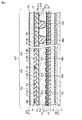
VAモードなどの主として縦電界を利用するモードの表示パネルPNLでは、アレイ基板ARにおいて、有機絶縁膜である第1絶縁膜11の表面に画素電極PE及び外周配線CNが形成され、対向基板CTにおいて、オーバーコート層OCの表面に共通電極CEが形成される。このとき、アクティブエリアACTでは、メインスペーサMS2及びサブスペーサSS2がオーバーコート層OCの表面あるいは共通電極CEの表面に形成され、メインスペーサMS2がセルギャップを形成する一方で、サブスペーサSS2はアレイ基板ARから離間している。また、周辺エリアPRPでは、メインスペーサMS1及びサブスペーサSS1がオーバーコート層OCの表面あるいは共通電極CEの表面に形成され、メインスペーサMS1が外周配線CNと重ならない位置でセルギャップを維持するとともに、サブスペーサSS2が外周配線CNと重なる位置でセルギャップを維持している。このような表示パネルについても、上記の実施形態で説明したのと同様の効果が得られる。
ACT…アクティブエリア PRP…周辺エリア MT…実装部
MS1…メインスペーサ(周辺エリア) MS2…メインスペーサ(アクティブエリア) SS1…サブスペーサ(周辺エリア) SS2…サブスペーサ(アクティブエリア)
CN…外周配線
Claims (7)
- 画像を表示するアクティブエリアに配置されるとともに前記アクティブエリアの外側の周辺エリアに延在した第1表面及び第1裏面を有する無機絶縁膜と、前記アクティブエリアにおいて前記第1表面に形成された画素電極と、前記周辺エリアにおいて前記第1表面に形成された外周配線と、前記アクティブエリアにおいて前記第1裏面に形成された共通電極と、を備えた第1基板と、
前記第1表面に対向し前記アクティブエリア及び前記周辺エリアに亘って延在した第2表面を有する絶縁膜を備えた第2基板と、
前記周辺エリアにおいて前記無機絶縁膜と前記絶縁膜との間に位置し、第1高さを有する第1メインスペーサと、
前記周辺エリアにおいて前記外周配線と前記絶縁膜との間に位置し、前記第1高さよりも低い第2高さを有する第1サブスペーサと、
前記第1基板と前記第2基板との間に保持された液晶層と、
を備え、
前記第1基板は、さらに、絶縁基板と、前記絶縁基板と前記無機絶縁膜との間に位置する駆動配線と、を備え、
前記外周配線は、前記駆動配線の直上に位置している、液晶表示装置。 - 前記第1メインスペーサ及び前記第1サブスペーサは、前記第2表面に形成された、請求項1に記載の液晶表示装置。
- さらに、前記アクティブエリアに配置され、前記第1基板に接触し、前記第1メインスペーサと同等の高さを有する第2メインスペーサと、
前記アクティブエリアに配置され、前記第1基板から離間し、前記第1サブスペーサと同等の高さを有する第2サブスペーサと、を備えた、請求項2に記載の液晶表示装置。 - 前記外周配線の厚みは、前記画素電極の厚みより大きい、請求項1に記載の液晶表示装置。
- 前記第1基板は、さらに、信号供給源が実装される実装部と、前記アクティブエリアを挟んで対向する第1基板端部及び第3基板端部と、前記アクティブエリアを挟んで前記実装部と対向する第2基板端部と、を備え、
前記外周配線は、前記実装部から前記第1基板端部及び前記第3基板端部に沿った前記周辺エリアに配置された、請求項1に記載の液晶表示装置。 - 前記周辺エリアのうち、前記第1基板端部及び前記第3基板端部に沿った領域においては、前記第1サブスペーサの個数が前記第1メインスペーサの個数よりも多い、請求項5に記載の液晶表示装置。
- 前記第2高さと前記外周配線の厚みとの和は、前記第1高さに等しい、請求項4に記載の液晶表示装置。
Priority Applications (2)
| Application Number | Priority Date | Filing Date | Title |
|---|---|---|---|
| JP2014058133A JP6401923B2 (ja) | 2014-03-20 | 2014-03-20 | 液晶表示装置 |
| US14/662,681 US9798194B2 (en) | 2014-03-20 | 2015-03-19 | Liquid crystal display device |
Applications Claiming Priority (1)
| Application Number | Priority Date | Filing Date | Title |
|---|---|---|---|
| JP2014058133A JP6401923B2 (ja) | 2014-03-20 | 2014-03-20 | 液晶表示装置 |
Publications (2)
| Publication Number | Publication Date |
|---|---|
| JP2015184326A JP2015184326A (ja) | 2015-10-22 |
| JP6401923B2 true JP6401923B2 (ja) | 2018-10-10 |
Family
ID=54141966
Family Applications (1)
| Application Number | Title | Priority Date | Filing Date |
|---|---|---|---|
| JP2014058133A Active JP6401923B2 (ja) | 2014-03-20 | 2014-03-20 | 液晶表示装置 |
Country Status (2)
| Country | Link |
|---|---|
| US (1) | US9798194B2 (ja) |
| JP (1) | JP6401923B2 (ja) |
Families Citing this family (11)
| Publication number | Priority date | Publication date | Assignee | Title |
|---|---|---|---|---|
| CN105242435A (zh) * | 2015-11-02 | 2016-01-13 | 武汉华星光电技术有限公司 | 阵列基板及制作方法、液晶显示面板 |
| CN106019725A (zh) * | 2016-06-13 | 2016-10-12 | 京东方科技集团股份有限公司 | 基板、显示面板及显示装置 |
| JP6775404B2 (ja) * | 2016-12-15 | 2020-10-28 | 三菱電機株式会社 | 液晶表示装置 |
| CN106773356A (zh) | 2017-01-20 | 2017-05-31 | 京东方科技集团股份有限公司 | 一种显示面板及其制备方法和显示装置 |
| CN207352324U (zh) * | 2017-10-23 | 2018-05-11 | 中华映管股份有限公司 | 显示母板及显示面板 |
| JP2019101095A (ja) * | 2017-11-29 | 2019-06-24 | シャープ株式会社 | 液晶パネル |
| JP6556417B1 (ja) * | 2017-12-26 | 2019-08-07 | 堺ディスプレイプロダクト株式会社 | 有機el表示装置およびその製造方法 |
| CN208737161U (zh) * | 2018-09-21 | 2019-04-12 | 重庆惠科金渝光电科技有限公司 | 一种增大隔垫物段差的显示面板及显示器 |
| US10838261B2 (en) | 2018-11-19 | 2020-11-17 | Panasonic Liquid Crystal Display Co., Ltd. | Display devices |
| CN109683738B (zh) * | 2018-11-30 | 2021-07-06 | 武汉华星光电技术有限公司 | 显示面板 |
| CN114253035A (zh) * | 2020-09-23 | 2022-03-29 | 京东方科技集团股份有限公司 | 显示装置和阵列基板 |
Family Cites Families (16)
| Publication number | Priority date | Publication date | Assignee | Title |
|---|---|---|---|---|
| JP2803792B2 (ja) * | 1992-08-28 | 1998-09-24 | シャープ株式会社 | アクティブマトリクス型液晶表示装置 |
| US7683993B2 (en) * | 2005-02-25 | 2010-03-23 | Semiconductor Energy Laboratory Co., Ltd. | Liquid crystal display device |
| US7738068B2 (en) * | 2005-12-30 | 2010-06-15 | Lg. Display Co., Ltd. | Liquid crystal display device |
| KR100920481B1 (ko) | 2006-05-10 | 2009-10-08 | 엘지디스플레이 주식회사 | 횡전계 방식 액정표시장치와 그 제조방법 |
| KR100970925B1 (ko) * | 2006-12-29 | 2010-07-20 | 엘지디스플레이 주식회사 | 액정표시장치 및 이의 제조방법 |
| JP5239368B2 (ja) * | 2008-02-06 | 2013-07-17 | 三菱電機株式会社 | アレイ基板および表示装置 |
| JP5394655B2 (ja) * | 2008-04-28 | 2014-01-22 | 株式会社ジャパンディスプレイ | 液晶表示装置 |
| US8310609B2 (en) * | 2008-09-30 | 2012-11-13 | Sony Corporation | Liquid crystal device, electronic apparatus, and method of manufacturing liquid crystal device |
| JP5260424B2 (ja) * | 2009-07-08 | 2013-08-14 | 株式会社ジャパンディスプレイ | 液晶表示装置 |
| TW201137813A (en) * | 2010-04-29 | 2011-11-01 | Wintek Corp | Display panel |
| JP5786601B2 (ja) * | 2011-09-28 | 2015-09-30 | セイコーエプソン株式会社 | 電気光学装置、及び電子機器 |
| US9316859B2 (en) * | 2011-10-11 | 2016-04-19 | Lg Display Co., Ltd. | Liquid crystal display device and method for manufacturing the same |
| JP5972041B2 (ja) * | 2012-05-15 | 2016-08-17 | 三菱電機株式会社 | 液晶表示装置 |
| JP2014038210A (ja) * | 2012-08-16 | 2014-02-27 | Japan Display Inc | 液晶表示装置 |
| JP2014044330A (ja) * | 2012-08-27 | 2014-03-13 | Japan Display Inc | 液晶表示装置 |
| JP6030426B2 (ja) | 2012-12-07 | 2016-11-24 | 株式会社ジャパンディスプレイ | 液晶表示装置 |
-
2014
- 2014-03-20 JP JP2014058133A patent/JP6401923B2/ja active Active
-
2015
- 2015-03-19 US US14/662,681 patent/US9798194B2/en not_active Expired - Fee Related
Also Published As
| Publication number | Publication date |
|---|---|
| US9798194B2 (en) | 2017-10-24 |
| US20150268504A1 (en) | 2015-09-24 |
| JP2015184326A (ja) | 2015-10-22 |
Similar Documents
| Publication | Publication Date | Title |
|---|---|---|
| JP6401923B2 (ja) | 液晶表示装置 | |
| US9176339B2 (en) | Liquid crystal display device | |
| US10134906B2 (en) | Display device | |
| JP5530987B2 (ja) | 液晶表示装置 | |
| JP4999127B2 (ja) | 液晶表示装置 | |
| JP5906043B2 (ja) | 液晶表示装置 | |
| JP5636342B2 (ja) | 液晶表示装置 | |
| US10429688B2 (en) | Liquid crystal display device | |
| JP5526085B2 (ja) | 液晶表示装置 | |
| JP5647955B2 (ja) | 液晶表示装置 | |
| JP2012113125A (ja) | 液晶表示パネル及び液晶表示装置 | |
| JP2015084017A (ja) | 液晶表示装置 | |
| JP2013088555A (ja) | 液晶表示装置 | |
| JP2017191276A (ja) | 液晶表示装置 | |
| JP2019124887A (ja) | 液晶パネル | |
| JP2017111328A (ja) | 液晶表示装置 | |
| JP2015014670A (ja) | 液晶表示装置 | |
| JP2015049391A (ja) | 液晶表示装置 | |
| US9915840B2 (en) | Liquid crystal display device | |
| JP2014038210A (ja) | 液晶表示装置 | |
| JP2015094909A (ja) | 液晶表示装置 | |
| JP6030426B2 (ja) | 液晶表示装置 | |
| JP2013041022A (ja) | 液晶表示装置 | |
| JP5197873B2 (ja) | 液晶表示装置 | |
| JP2018205601A (ja) | 液晶表示パネル |
Legal Events
| Date | Code | Title | Description |
|---|---|---|---|
| A621 | Written request for application examination |
Free format text: JAPANESE INTERMEDIATE CODE: A621 Effective date: 20170106 |
|
| A131 | Notification of reasons for refusal |
Free format text: JAPANESE INTERMEDIATE CODE: A131 Effective date: 20170829 |
|
| A977 | Report on retrieval |
Free format text: JAPANESE INTERMEDIATE CODE: A971007 Effective date: 20170830 |
|
| A521 | Request for written amendment filed |
Free format text: JAPANESE INTERMEDIATE CODE: A523 Effective date: 20171016 |
|
| A131 | Notification of reasons for refusal |
Free format text: JAPANESE INTERMEDIATE CODE: A131 Effective date: 20180313 |
|
| A521 | Request for written amendment filed |
Free format text: JAPANESE INTERMEDIATE CODE: A523 Effective date: 20180418 |
|
| TRDD | Decision of grant or rejection written | ||
| A01 | Written decision to grant a patent or to grant a registration (utility model) |
Free format text: JAPANESE INTERMEDIATE CODE: A01 Effective date: 20180828 |
|
| A61 | First payment of annual fees (during grant procedure) |
Free format text: JAPANESE INTERMEDIATE CODE: A61 Effective date: 20180910 |
|
| R150 | Certificate of patent or registration of utility model |
Ref document number: 6401923 Country of ref document: JP Free format text: JAPANESE INTERMEDIATE CODE: R150 |
|
| R250 | Receipt of annual fees |
Free format text: JAPANESE INTERMEDIATE CODE: R250 |
|
| R250 | Receipt of annual fees |
Free format text: JAPANESE INTERMEDIATE CODE: R250 |
|
| R250 | Receipt of annual fees |
Free format text: JAPANESE INTERMEDIATE CODE: R250 |