JP6401248B2 - LED having scattering mechanism in substrate - Google Patents
LED having scattering mechanism in substrate Download PDFInfo
- Publication number
- JP6401248B2 JP6401248B2 JP2016513467A JP2016513467A JP6401248B2 JP 6401248 B2 JP6401248 B2 JP 6401248B2 JP 2016513467 A JP2016513467 A JP 2016513467A JP 2016513467 A JP2016513467 A JP 2016513467A JP 6401248 B2 JP6401248 B2 JP 6401248B2
- Authority
- JP
- Japan
- Prior art keywords
- substrate
- light
- semiconductor layer
- led semiconductor
- scattering regions
- Prior art date
- Legal status (The legal status is an assumption and is not a legal conclusion. Google has not performed a legal analysis and makes no representation as to the accuracy of the status listed.)
- Active
Links
- 239000000758 substrate Substances 0.000 title claims description 93
- 230000007246 mechanism Effects 0.000 title description 2
- 239000004065 semiconductor Substances 0.000 claims description 34
- OAICVXFJPJFONN-UHFFFAOYSA-N Phosphorus Chemical compound [P] OAICVXFJPJFONN-UHFFFAOYSA-N 0.000 claims description 30
- 238000000149 argon plasma sintering Methods 0.000 claims description 28
- 239000002245 particle Substances 0.000 claims description 15
- 229910052751 metal Inorganic materials 0.000 claims description 13
- 239000002184 metal Substances 0.000 claims description 13
- 239000000463 material Substances 0.000 claims description 5
- 239000000853 adhesive Substances 0.000 claims description 3
- 230000001070 adhesive effect Effects 0.000 claims description 3
- 239000002923 metal particle Substances 0.000 claims 1
- 238000000034 method Methods 0.000 description 8
- 238000000605 extraction Methods 0.000 description 7
- 230000031700 light absorption Effects 0.000 description 5
- 229920001296 polysiloxane Polymers 0.000 description 5
- 229910052594 sapphire Inorganic materials 0.000 description 5
- 239000010980 sapphire Substances 0.000 description 5
- 229910010413 TiO 2 Inorganic materials 0.000 description 3
- 239000007788 liquid Substances 0.000 description 3
- 239000004593 Epoxy Substances 0.000 description 2
- 240000003380 Passiflora rubra Species 0.000 description 2
- BQCADISMDOOEFD-UHFFFAOYSA-N Silver Chemical compound [Ag] BQCADISMDOOEFD-UHFFFAOYSA-N 0.000 description 2
- 239000011230 binding agent Substances 0.000 description 2
- 239000013590 bulk material Substances 0.000 description 2
- 238000001962 electrophoresis Methods 0.000 description 2
- 238000012986 modification Methods 0.000 description 2
- 230000004048 modification Effects 0.000 description 2
- 230000005855 radiation Effects 0.000 description 2
- 238000007650 screen-printing Methods 0.000 description 2
- 229910052709 silver Inorganic materials 0.000 description 2
- 239000004332 silver Substances 0.000 description 2
- 239000011800 void material Substances 0.000 description 2
- 238000010146 3D printing Methods 0.000 description 1
- JMASRVWKEDWRBT-UHFFFAOYSA-N Gallium nitride Chemical compound [Ga]#N JMASRVWKEDWRBT-UHFFFAOYSA-N 0.000 description 1
- 238000010521 absorption reaction Methods 0.000 description 1
- 229910052782 aluminium Inorganic materials 0.000 description 1
- XAGFODPZIPBFFR-UHFFFAOYSA-N aluminium Chemical compound [Al] XAGFODPZIPBFFR-UHFFFAOYSA-N 0.000 description 1
- 210000000007 bat wing Anatomy 0.000 description 1
- 239000000919 ceramic Substances 0.000 description 1
- 230000001627 detrimental effect Effects 0.000 description 1
- 239000011521 glass Substances 0.000 description 1
- 238000010030 laminating Methods 0.000 description 1
- 238000003475 lamination Methods 0.000 description 1
- 238000004519 manufacturing process Methods 0.000 description 1
- 238000000465 moulding Methods 0.000 description 1
- 239000004033 plastic Substances 0.000 description 1
- 239000000843 powder Substances 0.000 description 1
- 238000002310 reflectometry Methods 0.000 description 1
- 238000004088 simulation Methods 0.000 description 1
- 239000012780 transparent material Substances 0.000 description 1
Images


Classifications
-
- H—ELECTRICITY
- H01—ELECTRIC ELEMENTS
- H01L—SEMICONDUCTOR DEVICES NOT COVERED BY CLASS H10
- H01L33/00—Semiconductor devices having potential barriers specially adapted for light emission; Processes or apparatus specially adapted for the manufacture or treatment thereof or of parts thereof; Details thereof
- H01L33/48—Semiconductor devices having potential barriers specially adapted for light emission; Processes or apparatus specially adapted for the manufacture or treatment thereof or of parts thereof; Details thereof characterised by the semiconductor body packages
- H01L33/58—Optical field-shaping elements
- H01L33/60—Reflective elements
-
- H—ELECTRICITY
- H01—ELECTRIC ELEMENTS
- H01L—SEMICONDUCTOR DEVICES NOT COVERED BY CLASS H10
- H01L33/00—Semiconductor devices having potential barriers specially adapted for light emission; Processes or apparatus specially adapted for the manufacture or treatment thereof or of parts thereof; Details thereof
- H01L33/02—Semiconductor devices having potential barriers specially adapted for light emission; Processes or apparatus specially adapted for the manufacture or treatment thereof or of parts thereof; Details thereof characterised by the semiconductor bodies
-
- H—ELECTRICITY
- H01—ELECTRIC ELEMENTS
- H01L—SEMICONDUCTOR DEVICES NOT COVERED BY CLASS H10
- H01L33/00—Semiconductor devices having potential barriers specially adapted for light emission; Processes or apparatus specially adapted for the manufacture or treatment thereof or of parts thereof; Details thereof
- H01L33/36—Semiconductor devices having potential barriers specially adapted for light emission; Processes or apparatus specially adapted for the manufacture or treatment thereof or of parts thereof; Details thereof characterised by the electrodes
-
- H—ELECTRICITY
- H01—ELECTRIC ELEMENTS
- H01L—SEMICONDUCTOR DEVICES NOT COVERED BY CLASS H10
- H01L33/00—Semiconductor devices having potential barriers specially adapted for light emission; Processes or apparatus specially adapted for the manufacture or treatment thereof or of parts thereof; Details thereof
- H01L33/48—Semiconductor devices having potential barriers specially adapted for light emission; Processes or apparatus specially adapted for the manufacture or treatment thereof or of parts thereof; Details thereof characterised by the semiconductor body packages
- H01L33/50—Wavelength conversion elements
- H01L33/501—Wavelength conversion elements characterised by the materials, e.g. binder
- H01L33/502—Wavelength conversion materials
-
- H—ELECTRICITY
- H01—ELECTRIC ELEMENTS
- H01L—SEMICONDUCTOR DEVICES NOT COVERED BY CLASS H10
- H01L33/00—Semiconductor devices having potential barriers specially adapted for light emission; Processes or apparatus specially adapted for the manufacture or treatment thereof or of parts thereof; Details thereof
- H01L33/48—Semiconductor devices having potential barriers specially adapted for light emission; Processes or apparatus specially adapted for the manufacture or treatment thereof or of parts thereof; Details thereof characterised by the semiconductor body packages
- H01L33/50—Wavelength conversion elements
- H01L33/507—Wavelength conversion elements the elements being in intimate contact with parts other than the semiconductor body or integrated with parts other than the semiconductor body
-
- H—ELECTRICITY
- H01—ELECTRIC ELEMENTS
- H01L—SEMICONDUCTOR DEVICES NOT COVERED BY CLASS H10
- H01L33/00—Semiconductor devices having potential barriers specially adapted for light emission; Processes or apparatus specially adapted for the manufacture or treatment thereof or of parts thereof; Details thereof
- H01L33/48—Semiconductor devices having potential barriers specially adapted for light emission; Processes or apparatus specially adapted for the manufacture or treatment thereof or of parts thereof; Details thereof characterised by the semiconductor body packages
- H01L33/50—Wavelength conversion elements
- H01L33/508—Wavelength conversion elements having a non-uniform spatial arrangement or non-uniform concentration, e.g. patterned wavelength conversion layer, wavelength conversion layer with a concentration gradient of the wavelength conversion material
-
- H—ELECTRICITY
- H01—ELECTRIC ELEMENTS
- H01L—SEMICONDUCTOR DEVICES NOT COVERED BY CLASS H10
- H01L2933/00—Details relating to devices covered by the group H01L33/00 but not provided for in its subgroups
- H01L2933/0091—Scattering means in or on the semiconductor body or semiconductor body package
Landscapes
- Engineering & Computer Science (AREA)
- Microelectronics & Electronic Packaging (AREA)
- Manufacturing & Machinery (AREA)
- Computer Hardware Design (AREA)
- Power Engineering (AREA)
- Led Device Packages (AREA)
- Led Devices (AREA)
Description
本発明は、発光ダイオード(LED)に関し、特に、LEDダイ内で光を散乱する技術に関する。 The present invention relates to light emitting diodes (LEDs), and more particularly to techniques for scattering light within an LED die.
青色光を発するGaN系LEDにおいて、成長基板は典型的に、透明なサファイア基板、SiC基板、又はGaN基板である。フリップチップLEDでは、光は活性層によって生成されて透明基板を通って出て行く。 In GaN-based LEDs that emit blue light, the growth substrate is typically a transparent sapphire substrate, SiC substrate, or GaN substrate. In flip chip LEDs, light is generated by the active layer and exits through the transparent substrate.
図1は、従来のGaN系フリップチップLEDダイ10を例示している。半導体層は、N型層12、活性層14(量子井戸を形成する)、及びP型層16を含んでいる。これらの層は、典型的にはサファイアである透明な成長基板18の表面上に成長される。基板18の頂部上に蛍光体層20が堆積される。蛍光体粒子22が、活性層14によって放出された青色光によって活性化されて、光を波長シフトさせる。蛍光体の発色が黄色である場合、黄色光と青色光との組み合わせが白色光を作り出す。このようにして、実質的に如何なる色の光も作り出され得る。
FIG. 1 illustrates a conventional GaN-based flip-chip LED die 10. The semiconductor layer includes an N-
光取り出し効率は、生成された光子のうちLEDダイ10を脱出する割合に関係する。LEDダイを設計することにおける1つの目標は、光取り出し効率を高めるよう、光吸収を最小化することである。光吸収に対する1つの寄与は、基板18の内部に捕捉されている光線24によって示した、基板18による全反射(total internal reflection;TIR)であり、基板18が導光体(光ガイド)として機能する。材料同士の境界面における一致しない屈折率が、浅い角度においてそのような反射を生じさせる。大雑把な近似として、GaNの屈折率(n)は2.5−3であり、サファイアの屈折率は1.77であり、蛍光体の屈折率は1.6−1.8であり、空気の屈折率は1である。
The light extraction efficiency is related to the proportion of the generated photons that escape the
さらに、LED半導体層、底部メタルコンタクト、及びコンタクト同士間の空間は、異なる反射率を有する。図1に示した例において、露出されたP型層16に接触しているPメタルコンタクト26は銀(Ag)であり、故に、高度に反射性(>95%)である。P型層16及び活性層14をエッチング除去して、Nメタルコンタクト28とN型層12との間のオーミックコンタクトを可能にした領域では、例えばアルミニウムなどの、より低い反射性の金属が使用されるとともに、これらのコンタクト領域では光は生成されない。コンタクト26と28との間にも、光を反射しない空間が存在する。光の吸収も行う半導体機構も存在し得る。蛍光体発光は概して等方的であり、故に、例えば光線30など、それらの光のうちの有意な割合が、LEDダイ10の光吸収のある領域に突き当たる。別の光線32が、基板18の側面でLEDダイ10内に戻るように全反射されて部分的に吸収されるとして示されている。光線33が、Pメタルコンタクト26によって効率的に反射されるとして示されている。
Furthermore, the LED semiconductor layer, the bottom metal contact, and the space between the contacts have different reflectivities. In the example shown in FIG. 1, the
吸収のある領域の全てが、LEDダイの光取り出し効率を低下させる。 All of the absorbed areas reduce the light extraction efficiency of the LED die.
LEDダイ内での光の吸収を低減することによって光取り出し効率を高める技術が望まれる。 Techniques are desired that increase light extraction efficiency by reducing light absorption within the LED die.
一実施形態において、LEDダイの透明成長基板が、例えばレーザ又はその他の方法を用いて形成されたボイド(空隙)などの、光散乱領域を有するように形成される。他の一実施形態において、成長基板が除去され、光散乱領域を含有した別の透明基板で置き換えられる。一実施形態において、光を生成しないLEDダイの光吸収性領域の一部又は全ての上に光散乱領域が形成されて、これら吸収性領域上への入射光の量が低減されるとともに、基板の側面にわたって光散乱領域が形成されて導光(光ガイディング)が抑制される。 In one embodiment, the transparent growth substrate of the LED die is formed to have a light scattering region, such as a void formed using a laser or other method. In another embodiment, the growth substrate is removed and replaced with another transparent substrate containing a light scattering region. In one embodiment, light scattering regions are formed over some or all of the light absorbing regions of the LED die that do not generate light, reducing the amount of incident light on these absorbing regions, and the substrate. A light-scattering region is formed over the side surfaces of the light and light guiding (light guiding) is suppressed.
上記基板が成長基板を置き換える場合、上記基板は、選択された領域に、例えばTiO2粒子又は反射金属フレーク(金属片)などの反射粒子を含むように形成され得る。反射領域を含有する基板層を積層することによって3D構造が形成されてもよい。 When the substrate replaces the growth substrate, the substrate can be formed to include reflective particles, such as TiO 2 particles or reflective metal flakes (metal pieces), in selected areas. A 3D structure may be formed by laminating a substrate layer containing a reflective region.
他の一実施形態において、上記基板は、光を散乱する側壁を有するように形成された不透明な蛍光体層である。 In another embodiment, the substrate is an opaque phosphor layer formed with side walls that scatter light.
この蛍光体層は、LEDの頂部に取り付けられるタイルとすることができ、あるいは液体バインダ内の粒子として堆積されることができ、あるいは電気泳動法によって堆積されることができ、あるいはその他の方法によって堆積され得る。 This phosphor layer can be a tile attached to the top of the LED, or can be deposited as particles in a liquid binder, or can be deposited by electrophoresis, or by other methods. Can be deposited.
その他の実施形態も記述される。 Other embodiments are also described.
図2は、基板38を除いて図1のLEDダイ10と同じとし得るLED36を例示している。基板38は、LED半導体が上にエピタキシャル成長されている基板とすることができ、あるいは、成長基板が除去された後にLED半導体層に取り付けられた基板とし得る。基板38内での導光(光ガイディング)を抑制するために、基板38は、光吸収性の領域の一部又は全てにわたって光散乱領域40A、40B及び40Cを有するとともに、側壁の一部又は全てにわたって光散乱領域42A及び42Bを有するように形成されている。散乱領域42A及び42Bは、側壁を周る連続的な散乱領域リングの一部とし得る。
FIG. 2 illustrates an
一実施形態において、基板38は、LED半導体層が上にエピタキシャル成長されているサファイア成長基板である。散乱領域40A−40C、42A及び42Bは、半導体層が成長される前又は後に、ボイドのアレイとして形成され得る。散乱領域40A−40C、42A及び42Bは、例えば多面体又は丸みのあるものなど、如何なる3D形状を有していてもよい。ボイドを作製することにはパルスレーザを用い得る。透明材料内にドット(ボイド)を用いて像を書き込む又は作り出すためのパルスレーザの使用はよく知られているが、この技術は、LEDダイ内で光を散乱させることには使用されてこなかった。
In one embodiment, the
他の一実施形態において、半導体層が成長された後に、例えばレーザリフトオフによってなどで成長基板が除去され、例えばN型層12に対してなど半導体層に対して、別の基板が取り付けられる。このような基板は、例えば、ガラス、サファイア、SiC、プラスチック、エポキシ、又はセラミックとし得る。基板38はLED半導体層に、例えばエポキシ若しくはシリコーンなどの何らかの好適な接着剤によって取り付けられ、あるいは、基板材料を直接的にLED半導体層に融合させることによって取り付けられ得る。取り付け基板では、散乱領域40A−40C、42A及び42Bは、ボイド又は光散乱粒子として形成され得る。基板38は、選択された領域内にボイドを形成するようにパルスレーザ処理を受け、あるいは選択された領域内に光散乱粒子を含むようにモールド成形され得る。成形する場合、大判基板ウェハ金型が用意され、基板材料が液体形態にある間に、スクリーン印刷プロセス又はその他のプロセスを用いて、選択領域内に反射粒子が注入され得る。そして、成形された基板が硬化され、成長基板が除去された後のLEDウェハに取り付けられる。例えばレイヤ積層(図9に示す)又は3Dプリント法を用いるなど、基板38を形成するためのその他の手法も想定される。取り付けられた基板は、そして、残りのLED製造プロセスにおいて機械的支持を提供する。その後、LEDウェハが個片化される。
In another embodiment, after the semiconductor layer is grown, the growth substrate is removed, such as by laser lift-off, and another substrate is attached to the semiconductor layer, such as for the N-
反射粒子は、例えば、TiO2フレーク、又はAgフレークなどの反射金属フレークとし得る。一実施形態において、これらのフレークは0.1−10ミクロン幅の範囲内とし得る。これらのフレークは光を散乱することを意図しているので、フレークの反射表面はランダムな角度にあるようにし得る。LEDダイの典型的な幅は1mm程度である。 The reflective particles may be, for example, reflective metal flakes such as TiO 2 flakes or Ag flakes. In one embodiment, these flakes can be in the range of 0.1-10 microns wide. Since these flakes are intended to scatter light, the reflective surface of the flakes can be at a random angle. The typical width of the LED die is on the order of 1 mm.
図2の例において、散乱領域40A、40B及び40Cは概して、光が生成されないところであるLEDダイの非活性部分の上に形成されている。故に、散乱領域40A−40Cは、上向きに放射された光を阻止しない。散乱領域40A−40Cはまた、好ましくは、例えばメタルコンタクト26と28との間又はNメタルコンタクト28の上など、反射性の乏しい表面である領域の上に形成される。コンタクト26と28との間を通る光は、典型的に劣った反射体である下に位置するサブマウント又は印刷回路基板によって上向きに反射されなければならないことになる。好ましくは、P型層16とのコンタクトを取るために使用される高度に反射性の銀コンタクト26の上には、散乱領域は存在しない。
In the example of FIG. 2, the
各散乱領域40A−40Cの形状は、下に位置する具体的な遮られるべき領域に合わせて調整され得る。それらの形状は、矩形、円形、等々とし得る。各散乱領域40A−40Cの厚さは、散乱領域40A−40Cの構造に依存する。例えば、散乱領域40A−40Cが反射フレークを含有し、且つ、フレークの非常に薄い層のみが、下に位置する領域に光が突き当たることを十分に阻止するために必要な場合には、薄い層のみが必要とされる。この層は10ミクロンほどの薄さとし得るが、典型的にはおおよそ50ミクロン厚になる。
The shape of each
一実施形態において、基板38はおよそ75−300ミクロン厚である。故に、基板38の底部近くの散乱領域40A−40Cは、蛍光体層20から25−250ミクロン離れ得る。
In one embodiment, the
図2及び一部のその他の図において、蛍光体層20はLEDダイの頂部の上のみに示されている。しかしながら、蛍光体層は、全ての実施形態において、基板38及び半導体層の側壁をも覆っていてもよい。
In FIG. 2 and some other views,
図3は、活性層14及び蛍光体粒子22によって生成されて散乱領域に突き当たる様々な光線を例示している。光線46は、活性層14によって生成され、散乱領域42Bによって、入射角でというよりも、様々な方向に散乱され、故に、基板38は非常に劣った導光体(光ガイド)になる(すなわち、光が2、3回のみの反射の後に脱出することになる)。
FIG. 3 illustrates various rays generated by the
光線48は、蛍光体粒子22Aから発せられ、散乱領域40Aによって、光吸収性の領域を避けるように向け直されている。光線50は、蛍光体粒子22Bによって発せられ、Pメタルコンタクト26で反射されている。光線52は、蛍光体粒子22Cによって発せられ、散乱領域42A内の複数の反射表面によって、上向き及び下向きの双方に向け直されている。
The
図4は、LEDダイの吸収性の領域の上に位置した、あるいはLEDダイの非光生成領域の上に位置した、基板57の頂部付近に、散乱領域56A−56Cが形成されてもよいことを例示している。光線58が、散乱領域56Aで反射されて、半導体層又は下に位置する層による吸収を回避するとして示されている。
FIG. 4 shows that scattering
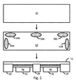
図5は、図4のLED構造がどのようにして形成され得るかを例示している。LED半導体層が成長された後、成長基板が除去され、N型層12の頂面に基板57が取り付けられる。接着剤として、シリコーンの薄い層が使用され得る。この取付けは、真空環境内で熱及び圧力の下で実行され得る。他の例では、基板57が軟化されてN型層12に直接的に融合する。N型層12は、光取り出しを高めるため、及び接着を支援するために、先ず粗面化されてもよい。
FIG. 5 illustrates how the LED structure of FIG. 4 can be formed. After the LED semiconductor layer is grown, the growth substrate is removed and a
一実施形態において、散乱領域42A、42B及び56A−56Cは、基板ウェハが形成されるときに基板内に形作られる。
In one embodiment, the
そして、基板57の上に蛍光体層20が形成される。蛍光体層20はまた、基板57及びLED層の側面の上にも形成されてよい。一実施形態において、蛍光体層20は、シリコーンの薄い層を用いて基板57に取り付けられるタイルである。蛍光体層20はまた、液体として堆積されて硬化されてもよいし、電気泳動法によって堆積されてもよい。
Then, the
図6は、中央の散乱領域60と、基板64の側壁を形づくる散乱領域62A及び62Bとを有する他の一実施形態を例示している。散乱領域62A及び62Bは、側壁に沿った連続した散乱領域リングの一部とし得る。散乱領域は、光吸収を低減するための散乱領域の使用にとらわれずに、所望の発光パターンを達成するための場所に位置付けられてもよい。特定の発光パターンを達成することは、例えば放物面ミラー又はプロジェクタによってなどでLED像が拡大されるときに特に重要である。散乱領域62A及び62Bからの散乱が大きい場合、この実施形態は、蛍光体層20を通って出て行く光の量を増大させるはずである。これは、デバイスの表面にわたっての色の均一性を向上させる。
FIG. 6 illustrates another embodiment having a
中央散乱領域60が排除されてもよく、散乱領域62A及び62Bが、LEDダイからの側面放射を制限して正面放射を促進させる。
The
図7は、バットウィング(コウモリの翼)状の発光パターンを形成するための、別形状の散乱領域68を例示している。散乱領域68は、所望の発光パターンを提供するよう、上から下に眺めたときに、中央に正方形又は円形を形づくり得る。一実施形態において、散乱領域68の直径は約300ミクロンである。蛍光体層70が、デバイスの側面を覆って下方にサブマウント72又は印刷回路基板の表面まで延在するコンフォーマル(共形)層として示されている。基板73はまた、その側壁の部分を形づくる散乱領域をも有してよい。
FIG. 7 exemplifies another
図8は、蛍光体タイル78内に形成された側壁散乱領域76A及び76Bを例示している。散乱領域76A及び76Bは、側壁に沿った連続した散乱領域リングの一部とし得る。図8において、透明基板は使用されておらず、また、成長基板は除去されている。蛍光体タイル78は、シリコーンバインダに蛍光体粉末が注入され、半導体層に取り付けられるのに先立ってそれがプリフォームされたものとし得る。蛍光体ウェハを形成するときに金型内に反射フレークがスクリーン印刷され得る。この蛍光体ウェハを、その後、シリコーンの薄い層(<10ミクロン)を用いてLEDウェハの頂面に取り付けることができ、得られたウェハが最終的に個片化される。散乱領域76A及び76Bは側面放射を制限する。この構造において、蛍光体タイル78は基板としての役割も果たす。この構造は特に、自動車ヘッドライト及びプロジェクタに適し得る。
FIG. 8 illustrates
図9は、3D基板がどのようにして形成され得るかを例示しており、ここでは、散乱領域80A−80Cが、例えばスクリーン印刷又は金型を使用することなどによって第1の基板層82の頂面に形成され、続いて、熱及び圧力の下で第2の基板層84へのラミネーションが行われる。第2の基板層84は、その側壁を形づくる更なる散乱領域86A及び86Bを有するように示されている。基板材料の層を積み重ねることによって散乱領域の3Dパターンが形成され得る。斯くして、散乱領域が基板の内部に形成され得る。
FIG. 9 illustrates how a 3D substrate can be formed, where the scattering regions 80A-80C are formed on the
概して、散乱領域は、発光を整形するために当該散乱領域が使用されるのでない限り、性能にとって有害となる箇所には位置付けられない。シミュレーションを行って、光取り出し効率を最大化するのに最適な領域及び散乱領域形状を決定し得る。典型的に高度に吸収性であり且つ光を生成しない箇所は、LED半導体層のエッジを含む。一実施形態において、散乱領域は、光が生成されないところである半導体層のエッジの上に位置する基板の底部付近の単一のリングとして形成される。 Generally, the scattering region is not positioned where it is detrimental to performance unless the scattering region is used to shape the emission. Simulations can be performed to determine the optimal region and scattering region shapes to maximize light extraction efficiency. The locations that are typically highly absorptive and do not produce light include the edges of the LED semiconductor layer. In one embodiment, the scattering region is formed as a single ring near the bottom of the substrate located above the edge of the semiconductor layer where no light is generated.
一部の用途において、光を更に散乱させるため及び/又は光取り出しを向上させるために、基板表面がテクスチャ加工される。本発明は、そのような表面テクスチャ加工と、本発明の実施形態が光を散乱させるために(単に表面上ではなく)基板内に反射粒子又は反射ボイドの何れかを導入する点で異なる。 In some applications, the substrate surface is textured to further scatter light and / or improve light extraction. The present invention differs from such surface texturing in that embodiments of the present invention introduce either reflective particles or reflective voids in the substrate to scatter light (not just on the surface).
一実施形態において、取り付けられる基板は、例えば光拡散粒子(例えば、TiO2)を均一に注入された基板など、元来的に一部の光を散乱させるバルク材料で形成される。本発明の光散乱領域は、基板のバルク材料を変更することによって、特定の領域での散乱を促進させる。 In one embodiment, the attached substrate is formed of a bulk material that inherently scatters some light, such as a substrate uniformly implanted with light diffusing particles (eg, TiO 2 ). The light scattering region of the present invention promotes scattering in specific regions by changing the bulk material of the substrate.
LEDの特定の用途において、当該LEDダイは、他のLEDダイを備えたシステム内、又は反射チャンバ内に置かれる。そのような場合においては、外部で生成された光が当該LEDダイに突き当たる。本発明はまた、外部で光が生成される場合の当該LEDダイによる光吸収を低減するために使用されてもよい。従って、システム効率が向上される。 In certain LED applications, the LED die is placed in a system with other LED dies or in a reflection chamber. In such a case, externally generated light strikes the LED die. The present invention may also be used to reduce light absorption by the LED die when light is generated externally. Therefore, system efficiency is improved.
本発明の特定の実施形態を示して説明したが、当業者に明らかなように、より広い観点での本発明を逸脱することなく変形及び変更が為され得るのであり、故に、添付の請求項は、その範囲内に、本発明の真の精神及び範囲に入るような全ての変形及び変更を包含するものである。 While particular embodiments of the present invention have been shown and described, it will be apparent to those skilled in the art that changes and modifications can be made without departing from the invention in its broader aspects, and thus, the appended claims Is intended to encompass within its scope all such variations and modifications as fall within the true spirit and scope of the present invention.
Claims (14)
前記発光面の上に位置し、前記LED半導体層に取り付けられた基板と、
前記基板内に形成された1つ以上の光散乱領域と、
を有し、
前記LED半導体層は、光を生成する領域と、光を生成しない領域とを含み、前記1つ以上の光散乱領域は、光を生成しないLED半導体層領域のうちの少なくとも1つの上に配置され、
前記1つ以上の光散乱領域は、光を生成するLED半導体層領域の上には形成されていない、
発光デバイス。 A light emitting diode (LED) semiconductor layer that generates light, an LED semiconductor layer having a light emitting surface;
A substrate positioned on the light emitting surface and attached to the LED semiconductor layer;
One or more light scattering regions formed in the substrate;
Have
The LED semiconductor layer includes a region that generates light and a region that does not generate light, and the one or more light scattering regions are disposed on at least one of the LED semiconductor layer regions that do not generate light. ,
The one or more light scattering regions are not formed on the LED semiconductor layer region that generates light,
Light emitting device.
Applications Claiming Priority (3)
| Application Number | Priority Date | Filing Date | Title |
|---|---|---|---|
| US201361823528P | 2013-05-15 | 2013-05-15 | |
| US61/823,528 | 2013-05-15 | ||
| PCT/IB2014/061196 WO2014184701A1 (en) | 2013-05-15 | 2014-05-05 | Led with scattering features in substrate |
Publications (3)
| Publication Number | Publication Date |
|---|---|
| JP2016521463A JP2016521463A (en) | 2016-07-21 |
| JP2016521463A5 JP2016521463A5 (en) | 2017-05-25 |
| JP6401248B2 true JP6401248B2 (en) | 2018-10-10 |
Family
ID=50792485
Family Applications (1)
| Application Number | Title | Priority Date | Filing Date |
|---|---|---|---|
| JP2016513467A Active JP6401248B2 (en) | 2013-05-15 | 2014-05-05 | LED having scattering mechanism in substrate |
Country Status (7)
| Country | Link |
|---|---|
| US (3) | US9508908B2 (en) |
| EP (1) | EP2997606B1 (en) |
| JP (1) | JP6401248B2 (en) |
| KR (1) | KR102222215B1 (en) |
| CN (2) | CN105531833B (en) |
| TW (2) | TWI641161B (en) |
| WO (1) | WO2014184701A1 (en) |
Families Citing this family (48)
| Publication number | Priority date | Publication date | Assignee | Title |
|---|---|---|---|---|
| KR102222215B1 (en) * | 2013-05-15 | 2021-03-03 | 루미리즈 홀딩 비.브이. | Led with scattering features in substrate |
| DE102014100772B4 (en) * | 2014-01-23 | 2022-11-03 | OSRAM Opto Semiconductors Gesellschaft mit beschränkter Haftung | Method for producing optoelectronic semiconductor components and optoelectronic semiconductor component |
| JP2018060868A (en) * | 2016-10-03 | 2018-04-12 | 株式会社ディスコ | Method for manufacturing light-emitting diode chip and light-emitting diode chip |
| JP2018074109A (en) * | 2016-11-04 | 2018-05-10 | 株式会社ディスコ | Method for manufacturing light-emitting diode chip and light-emitting diode chip |
| JP2018074110A (en) * | 2016-11-04 | 2018-05-10 | 株式会社ディスコ | Method for manufacturing light-emitting diode chip and light-emitting diode chip |
| JP2018113386A (en) * | 2017-01-13 | 2018-07-19 | 株式会社ディスコ | Method for manufacturing light-emitting diode chip and light-emitting diode chip |
| JP2018113387A (en) * | 2017-01-13 | 2018-07-19 | 株式会社ディスコ | Method for manufacturing light-emitting diode chip and light-emitting diode chip |
| JP2018113384A (en) * | 2017-01-13 | 2018-07-19 | 株式会社ディスコ | Method for manufacturing light-emitting diode chip and light-emitting diode chip |
| JP2018113385A (en) * | 2017-01-13 | 2018-07-19 | 株式会社ディスコ | Method for manufacturing light-emitting diode chip and light-emitting diode chip |
| JP2018113388A (en) * | 2017-01-13 | 2018-07-19 | 株式会社ディスコ | Method for manufacturing light-emitting diode chip and light-emitting diode chip |
| JP2018116966A (en) * | 2017-01-16 | 2018-07-26 | 株式会社ディスコ | Method for manufacturing light-emitting diode chip and light-emitting diode chip |
| JP2018116965A (en) * | 2017-01-16 | 2018-07-26 | 株式会社ディスコ | Method for manufacturing light-emitting diode chip and light-emitting diode chip |
| JP6786166B2 (en) * | 2017-01-16 | 2020-11-18 | 株式会社ディスコ | Manufacturing method of light emitting diode chip and light emitting diode chip |
| JP2018116964A (en) * | 2017-01-16 | 2018-07-26 | 株式会社ディスコ | Method for manufacturing light-emitting diode chip and light-emitting diode chip |
| JP2018129343A (en) * | 2017-02-06 | 2018-08-16 | 株式会社ディスコ | Method for manufacturing light-emitting diode chip and light-emitting diode chip |
| JP2018129345A (en) * | 2017-02-06 | 2018-08-16 | 株式会社ディスコ | Method for manufacturing light-emitting diode chip and light-emitting diode chip |
| JP2018129341A (en) * | 2017-02-06 | 2018-08-16 | 株式会社ディスコ | Method for manufacturing light-emitting diode chip and light-emitting diode chip |
| JP2018129348A (en) * | 2017-02-06 | 2018-08-16 | 株式会社ディスコ | Method for manufacturing light-emitting diode chip and light-emitting diode chip and |
| JP2018129342A (en) * | 2017-02-06 | 2018-08-16 | 株式会社ディスコ | Method for manufacturing light-emitting diode chip and light-emitting diode chip |
| JP2018129346A (en) * | 2017-02-06 | 2018-08-16 | 株式会社ディスコ | Method for manufacturing light-emitting diode chip and light-emitting diode chip |
| JP2018129344A (en) * | 2017-02-06 | 2018-08-16 | 株式会社ディスコ | Method for manufacturing light-emitting diode chip and light-emitting diode chip |
| JP2018129347A (en) * | 2017-02-06 | 2018-08-16 | 株式会社ディスコ | Method for manufacturing light-emitting diode chip and light-emitting diode chip |
| JP2018129370A (en) * | 2017-02-07 | 2018-08-16 | 株式会社ディスコ | Method for manufacturing light-emitting diode chip and light-emitting diode chip |
| JP2018148013A (en) * | 2017-03-06 | 2018-09-20 | 株式会社ディスコ | Method for manufacturing light-emitting diode chip and light-emitting diode chip |
| JP2018148017A (en) * | 2017-03-06 | 2018-09-20 | 株式会社ディスコ | Method for manufacturing light-emitting diode chip and light-emitting diode chip |
| JP2018148014A (en) * | 2017-03-06 | 2018-09-20 | 株式会社ディスコ | Method for manufacturing light-emitting diode chip and light-emitting diode chip |
| JP2018148016A (en) * | 2017-03-06 | 2018-09-20 | 株式会社ディスコ | Method for manufacturing light-emitting diode chip and light-emitting diode chip |
| JP2018148015A (en) * | 2017-03-06 | 2018-09-20 | 株式会社ディスコ | Manufacturing method of light-emitting diode chip and light-emitting diode chip |
| JP2018182001A (en) * | 2017-04-10 | 2018-11-15 | 株式会社ディスコ | Method for manufacturing light-emitting diode chip and light-emitting diode chip |
| JP2018181998A (en) * | 2017-04-10 | 2018-11-15 | 株式会社ディスコ | Method for manufacturing light-emitting diode chip and light-emitting diode chip |
| JP2018182168A (en) * | 2017-04-18 | 2018-11-15 | 株式会社ディスコ | Method for manufacturing light-emitting diode chip and light-emitting diode chip |
| JP2018182166A (en) * | 2017-04-18 | 2018-11-15 | 株式会社ディスコ | Method for manufacturing light-emitting diode chip and light-emitting diode chip |
| JP6821260B2 (en) * | 2017-04-18 | 2021-01-27 | 株式会社ディスコ | Manufacturing method of light emitting diode chip and light emitting diode chip |
| JP2018182167A (en) * | 2017-04-18 | 2018-11-15 | 株式会社ディスコ | Method for manufacturing light-emitting diode chip and light-emitting diode chip |
| JP2018186169A (en) * | 2017-04-25 | 2018-11-22 | 株式会社ディスコ | Method for manufacturing light-emitting diode chip and light-emitting diode chip |
| JP2018186168A (en) * | 2017-04-25 | 2018-11-22 | 株式会社ディスコ | Method for manufacturing light-emitting diode chip and light-emitting diode chip |
| JP2018186167A (en) * | 2017-04-25 | 2018-11-22 | 株式会社ディスコ | Method for manufacturing light-emitting diode chip and light-emitting diode chip |
| JP2018186166A (en) * | 2017-04-25 | 2018-11-22 | 株式会社ディスコ | Method for manufacturing light-emitting diode chip and light-emitting diode chip |
| EP3428975A1 (en) * | 2017-07-14 | 2019-01-16 | AGC Glass Europe | Light-emitting devices having an antireflective silicon carbide or sapphire substrate and methods of forming the same |
| JP7418330B2 (en) | 2017-12-21 | 2024-01-19 | ルミレッズ ホールディング ベーフェー | lighting device |
| US11557703B2 (en) | 2017-12-21 | 2023-01-17 | Lumileds Llc | Light intensity adaptive LED sidewalls |
| US11054112B2 (en) | 2017-12-22 | 2021-07-06 | Lumileds Llc | Ceramic phosphor with lateral light barriers |
| US11430919B2 (en) * | 2019-04-26 | 2022-08-30 | Lumileds Llc | High brightness LEDs with non-specular nanostructured thin film reflectors |
| US11189757B2 (en) * | 2019-12-12 | 2021-11-30 | Lumileds Llc | Light emitting diodes with reflective sidewalls comprising porous particles |
| CN112289903B (en) * | 2020-07-30 | 2021-08-06 | 华灿光电(浙江)有限公司 | Light emitting diode chip and manufacturing method thereof |
| US20220199857A1 (en) * | 2020-12-17 | 2022-06-23 | Seoul Viosys Co., Ltd. | Unit pixel and displaying apparatus including the unit pixel |
| DE102021113095A1 (en) * | 2021-05-20 | 2022-11-24 | OSRAM Opto Semiconductors Gesellschaft mit beschränkter Haftung | Method for producing an optoelectronic component and optoelectronic component |
| US20230034456A1 (en) * | 2021-07-30 | 2023-02-02 | Seoul Viosys Co., Ltd. | Light emitting module and display apparatus by using the same |
Family Cites Families (50)
| Publication number | Priority date | Publication date | Assignee | Title |
|---|---|---|---|---|
| US5810463A (en) * | 1994-11-28 | 1998-09-22 | Nikon Corporation | Illumination device |
| US6562644B2 (en) * | 2000-08-08 | 2003-05-13 | Matsushita Electric Industrial Co., Ltd. | Semiconductor substrate, method of manufacturing the semiconductor substrate, semiconductor device and pattern forming method |
| JP3559827B2 (en) * | 2002-05-24 | 2004-09-02 | 独立行政法人理化学研究所 | Method and apparatus for processing inside transparent material |
| US6878969B2 (en) * | 2002-07-29 | 2005-04-12 | Matsushita Electric Works, Ltd. | Light emitting device |
| JP4329374B2 (en) * | 2002-07-29 | 2009-09-09 | パナソニック電工株式会社 | LIGHT EMITTING ELEMENT AND MANUFACTURING METHOD THEREOF |
| JP2005138169A (en) * | 2003-11-10 | 2005-06-02 | Gijutsu Transfer Service:Kk | Laser marking device, laser marking method, and marked body |
| JP2005158369A (en) * | 2003-11-21 | 2005-06-16 | Toyota Industries Corp | Optical member and lighting system |
| JP2005158370A (en) * | 2003-11-21 | 2005-06-16 | Toyota Industries Corp | Planar light source device and liquid crystal display device |
| JP2005158665A (en) * | 2003-11-24 | 2005-06-16 | Toyota Industries Corp | Lighting system |
| US7442964B2 (en) * | 2004-08-04 | 2008-10-28 | Philips Lumileds Lighting Company, Llc | Photonic crystal light emitting device with multiple lattices |
| JP4634129B2 (en) * | 2004-12-10 | 2011-02-16 | 三菱重工業株式会社 | Light scattering film and optical device using the same |
| DE102005048408B4 (en) * | 2005-06-10 | 2015-03-19 | Osram Opto Semiconductors Gmbh | Thin-film semiconductor body |
| JP2007109793A (en) * | 2005-10-12 | 2007-04-26 | Sony Corp | Semiconductor light-emitting element and light scattering substrate |
| JP2007184411A (en) | 2006-01-06 | 2007-07-19 | Sony Corp | Light emitting diode and its manufacturing method, integrated light emitting diode and its manufacturing method, light emitting diode backlight, light emitting diode lighting apparatus, light emitting diode display, electronic equipment, and electronic device and its manufacturing method |
| KR100780233B1 (en) * | 2006-05-15 | 2007-11-27 | 삼성전기주식회사 | Light emitting device with multi-pattern |
| EP2030258A2 (en) * | 2006-06-08 | 2009-03-04 | Koninklijke Philips Electronics N.V. | Light-emitting device |
| US8251538B2 (en) * | 2006-06-14 | 2012-08-28 | Koninklijke Philips Electronics N.V. | Lighting device |
| US7521862B2 (en) | 2006-11-20 | 2009-04-21 | Philips Lumileds Lighting Co., Llc | Light emitting device including luminescent ceramic and light-scattering material |
| JP5132961B2 (en) * | 2007-03-19 | 2013-01-30 | ハリソン東芝ライティング株式会社 | Optical semiconductor device and manufacturing method thereof |
| JP5373762B2 (en) * | 2007-04-03 | 2013-12-18 | コーニンクレッカ フィリップス エヌ ヴェ | Optical output device |
| JP2008270689A (en) * | 2007-04-25 | 2008-11-06 | Mitsubishi Chemicals Corp | GaN-BASED LIGHT EMITTING DIODE ELEMENT AND MANUFACTURING METHOD THEREOF |
| JP2009004625A (en) * | 2007-06-22 | 2009-01-08 | Sanken Electric Co Ltd | Semiconductor light emitting device |
| WO2009017035A1 (en) * | 2007-07-27 | 2009-02-05 | Asahi Glass Co., Ltd. | Translucent substrate, method for manufacturing the translucent substrate, organic led element and method for manufacturing the organic led element |
| US7863635B2 (en) * | 2007-08-07 | 2011-01-04 | Cree, Inc. | Semiconductor light emitting devices with applied wavelength conversion materials |
| EP2219416B1 (en) * | 2007-11-09 | 2018-02-14 | Asahi Glass Company, Limited | Light transmitting substrate, method for manufacturing light transmitting substrate, organic led element and method for manufacturing organic led element |
| KR101524012B1 (en) * | 2007-12-11 | 2015-05-29 | 코닌클리케 필립스 엔.브이. | Side emitting device with hybrid top reflector |
| US8177408B1 (en) * | 2008-02-15 | 2012-05-15 | Fusion Optix, Inc. | Light filtering directional control element and light fixture incorporating the same |
| US8408775B1 (en) * | 2008-03-12 | 2013-04-02 | Fusion Optix, Inc. | Light recycling directional control element and light emitting device using the same |
| DE102008030751A1 (en) * | 2008-06-27 | 2009-12-31 | Osram Opto Semiconductors Gmbh | Radiation-emitting semiconductor chip |
| KR20100018850A (en) * | 2008-08-07 | 2010-02-18 | 삼성모바일디스플레이주식회사 | Organic light emitting display device |
| US8129735B2 (en) * | 2008-09-24 | 2012-03-06 | Koninklijke Philips Electronics N.V. | LED with controlled angular non-uniformity |
| KR101064016B1 (en) * | 2008-11-26 | 2011-09-08 | 엘지이노텍 주식회사 | Light emitting device and manufacturing method |
| KR101809472B1 (en) * | 2009-01-14 | 2018-01-18 | 삼성전자주식회사 | Light emitting device for improving light extraction efficiency |
| US8110839B2 (en) * | 2009-07-13 | 2012-02-07 | Luxingtek, Ltd. | Lighting device, display, and method for manufacturing the same |
| US20110012147A1 (en) * | 2009-07-15 | 2011-01-20 | Koninklijke Philips Electronics N.V. | Wavelength-converted semiconductor light emitting device including a filter and a scattering structure |
| JP5379604B2 (en) * | 2009-08-21 | 2013-12-25 | 浜松ホトニクス株式会社 | Laser processing method and chip |
| CN102130051A (en) * | 2010-01-20 | 2011-07-20 | 晶元光电股份有限公司 | Light-emitting diode and manufacturing method thereof |
| DE102010027411A1 (en) * | 2010-07-15 | 2012-01-19 | Osram Opto Semiconductors Gmbh | Semiconductor component, substrate and method for producing a semiconductor layer sequence |
| US8210716B2 (en) * | 2010-08-27 | 2012-07-03 | Quarkstar Llc | Solid state bidirectional light sheet for general illumination |
| US8338199B2 (en) * | 2010-08-27 | 2012-12-25 | Quarkstar Llc | Solid state light sheet for general illumination |
| TW201214802A (en) * | 2010-09-27 | 2012-04-01 | Nat Univ Chung Hsing | Patterned substrate and LED formed using the same |
| US8455895B2 (en) * | 2010-11-08 | 2013-06-04 | Bridgelux, Inc. | LED-based light source utilizing asymmetric conductors |
| US9478719B2 (en) * | 2010-11-08 | 2016-10-25 | Bridgelux, Inc. | LED-based light source utilizing asymmetric conductors |
| DE102010063511A1 (en) * | 2010-12-20 | 2012-06-21 | Osram Opto Semiconductors Gmbh | Method for producing an optoelectronic component and optoelectronic component |
| KR101223225B1 (en) * | 2011-01-04 | 2013-01-31 | 갤럭시아포토닉스 주식회사 | Light emitting diode having light extracting layer formed in boundary regions and light emitting diode package |
| TWI470829B (en) * | 2011-04-27 | 2015-01-21 | Sino American Silicon Prod Inc | A method to fabrication an epitaxial substrate, a light emitting diode and the method to fabrication said light emitting diode |
| DE102012003638A1 (en) | 2012-02-24 | 2013-08-29 | Limo Patentverwaltung Gmbh & Co. Kg | led |
| US20140353705A1 (en) * | 2012-03-23 | 2014-12-04 | Sharp Kabushiki Kaisha | Semiconductor light emitting element, method of manufacturing semiconductor light emitting element, semiconductor light emitting device and substrate |
| US9512976B2 (en) | 2012-04-13 | 2016-12-06 | Sharp Kabushiki Kaisha | Light-emitting device, display device and illumination device |
| KR102222215B1 (en) * | 2013-05-15 | 2021-03-03 | 루미리즈 홀딩 비.브이. | Led with scattering features in substrate |
-
2014
- 2014-05-05 KR KR1020157035361A patent/KR102222215B1/en active IP Right Grant
- 2014-05-05 CN CN201480040511.4A patent/CN105531833B/en active Active
- 2014-05-05 CN CN201810026417.3A patent/CN108198918B/en active Active
- 2014-05-05 JP JP2016513467A patent/JP6401248B2/en active Active
- 2014-05-05 US US14/891,344 patent/US9508908B2/en active Active
- 2014-05-05 WO PCT/IB2014/061196 patent/WO2014184701A1/en active Application Filing
- 2014-05-05 EP EP14726207.5A patent/EP2997606B1/en active Active
- 2014-05-12 TW TW106132840A patent/TWI641161B/en active
- 2014-05-12 TW TW103116739A patent/TWI610461B/en active
-
2016
- 2016-10-26 US US15/335,354 patent/US9893253B2/en active Active
-
2017
- 2017-08-29 US US15/689,899 patent/US10074786B2/en active Active
Also Published As
| Publication number | Publication date |
|---|---|
| KR102222215B1 (en) | 2021-03-03 |
| TW201743464A (en) | 2017-12-16 |
| US20170047492A1 (en) | 2017-02-16 |
| US9508908B2 (en) | 2016-11-29 |
| CN108198918A (en) | 2018-06-22 |
| CN108198918B (en) | 2020-10-02 |
| EP2997606A1 (en) | 2016-03-23 |
| WO2014184701A1 (en) | 2014-11-20 |
| TW201507197A (en) | 2015-02-16 |
| US9893253B2 (en) | 2018-02-13 |
| US20160093782A1 (en) | 2016-03-31 |
| KR20160008610A (en) | 2016-01-22 |
| TWI610461B (en) | 2018-01-01 |
| CN105531833A (en) | 2016-04-27 |
| US10074786B2 (en) | 2018-09-11 |
| US20170358722A1 (en) | 2017-12-14 |
| TWI641161B (en) | 2018-11-11 |
| JP2016521463A (en) | 2016-07-21 |
| EP2997606B1 (en) | 2016-07-13 |
| CN105531833B (en) | 2018-01-30 |
Similar Documents
| Publication | Publication Date | Title |
|---|---|---|
| JP6401248B2 (en) | LED having scattering mechanism in substrate | |
| US8467633B2 (en) | Wavelength conversion structure and light source apparatus | |
| JP5526232B2 (en) | Light emitting diode with molded reflective sidewall coating | |
| US9890911B2 (en) | LED module with uniform phosphor illumination | |
| WO2007015844A2 (en) | Light emitting diodes with improved light extraction and reflectivity | |
| KR102087939B1 (en) | Light Emitting Device Package | |
| JP5543386B2 (en) | LIGHT EMITTING DEVICE, ITS MANUFACTURING METHOD, AND LIGHTING DEVICE | |
| JP2012195350A (en) | Light-emitting device and method of manufacturing the same | |
| JP2023009160A (en) | LED module with high near-field contrast ratio | |
| TWI741339B (en) | Light emitting device and method of manufacturing the same | |
| JP5853441B2 (en) | Light emitting device | |
| JP2009170188A (en) | Surface light source and display device | |
| KR20150042631A (en) | Optical lens and camera module having thereof | |
| KR20180036272A (en) | Optical lens, light emitting module and light unit having thereof | |
| JP2000277812A (en) | Line light source device and its manufacture | |
| JP2014510411A (en) | Semiconductor chip, display including a plurality of semiconductor chips, and manufacturing method thereof | |
| KR20180034929A (en) | Optical lens, light source module and light unit having thereof | |
| JP2012009696A (en) | Light emitting device and led illuminating equipment | |
| JP2016058551A (en) | Semiconductor light emitting device | |
| KR102435569B1 (en) | Optical lens, light emitting module and light unit having thereof | |
| JP2008147496A (en) | Light-emitting device | |
| KR102076240B1 (en) | Light Emitting Device |
Legal Events
| Date | Code | Title | Description |
|---|---|---|---|
| A521 | Request for written amendment filed |
Free format text: JAPANESE INTERMEDIATE CODE: A523 Effective date: 20170331 |
|
| A621 | Written request for application examination |
Free format text: JAPANESE INTERMEDIATE CODE: A621 Effective date: 20170331 |
|
| A977 | Report on retrieval |
Free format text: JAPANESE INTERMEDIATE CODE: A971007 Effective date: 20180131 |
|
| A131 | Notification of reasons for refusal |
Free format text: JAPANESE INTERMEDIATE CODE: A131 Effective date: 20180220 |
|
| A521 | Request for written amendment filed |
Free format text: JAPANESE INTERMEDIATE CODE: A523 Effective date: 20180517 |
|
| TRDD | Decision of grant or rejection written | ||
| A01 | Written decision to grant a patent or to grant a registration (utility model) |
Free format text: JAPANESE INTERMEDIATE CODE: A01 Effective date: 20180807 |
|
| A61 | First payment of annual fees (during grant procedure) |
Free format text: JAPANESE INTERMEDIATE CODE: A61 Effective date: 20180906 |
|
| R150 | Certificate of patent or registration of utility model |
Ref document number: 6401248 Country of ref document: JP Free format text: JAPANESE INTERMEDIATE CODE: R150 |
|
| S111 | Request for change of ownership or part of ownership |
Free format text: JAPANESE INTERMEDIATE CODE: R313113 |
|
| R350 | Written notification of registration of transfer |
Free format text: JAPANESE INTERMEDIATE CODE: R350 |
|
| R250 | Receipt of annual fees |
Free format text: JAPANESE INTERMEDIATE CODE: R250 |
|
| R250 | Receipt of annual fees |
Free format text: JAPANESE INTERMEDIATE CODE: R250 |
|
| R250 | Receipt of annual fees |
Free format text: JAPANESE INTERMEDIATE CODE: R250 |
|
| R250 | Receipt of annual fees |
Free format text: JAPANESE INTERMEDIATE CODE: R250 |