JP6400273B2 - Electrostatic chuck device - Google Patents
Electrostatic chuck device Download PDFInfo
- Publication number
- JP6400273B2 JP6400273B2 JP2013048185A JP2013048185A JP6400273B2 JP 6400273 B2 JP6400273 B2 JP 6400273B2 JP 2013048185 A JP2013048185 A JP 2013048185A JP 2013048185 A JP2013048185 A JP 2013048185A JP 6400273 B2 JP6400273 B2 JP 6400273B2
- Authority
- JP
- Japan
- Prior art keywords
- electrostatic chuck
- focus ring
- pedestal
- recess
- pedestal portion
- Prior art date
- Legal status (The legal status is an assumption and is not a legal conclusion. Google has not performed a legal analysis and makes no representation as to the accuracy of the status listed.)
- Active
Links
Images


Classifications
-
- H—ELECTRICITY
- H01—ELECTRIC ELEMENTS
- H01L—SEMICONDUCTOR DEVICES NOT COVERED BY CLASS H10
- H01L21/00—Processes or apparatus adapted for the manufacture or treatment of semiconductor or solid state devices or of parts thereof
- H01L21/67—Apparatus specially adapted for handling semiconductor or electric solid state devices during manufacture or treatment thereof; Apparatus specially adapted for handling wafers during manufacture or treatment of semiconductor or electric solid state devices or components ; Apparatus not specifically provided for elsewhere
- H01L21/683—Apparatus specially adapted for handling semiconductor or electric solid state devices during manufacture or treatment thereof; Apparatus specially adapted for handling wafers during manufacture or treatment of semiconductor or electric solid state devices or components ; Apparatus not specifically provided for elsewhere for supporting or gripping
- H01L21/6831—Apparatus specially adapted for handling semiconductor or electric solid state devices during manufacture or treatment thereof; Apparatus specially adapted for handling wafers during manufacture or treatment of semiconductor or electric solid state devices or components ; Apparatus not specifically provided for elsewhere for supporting or gripping using electrostatic chucks
Landscapes
- Engineering & Computer Science (AREA)
- Physics & Mathematics (AREA)
- Condensed Matter Physics & Semiconductors (AREA)
- General Physics & Mathematics (AREA)
- Manufacturing & Machinery (AREA)
- Computer Hardware Design (AREA)
- Microelectronics & Electronic Packaging (AREA)
- Power Engineering (AREA)
- Container, Conveyance, Adherence, Positioning, Of Wafer (AREA)
- Drying Of Semiconductors (AREA)
Description
本発明は、静電チャック装置に関する。 The present invention relates to an electrostatic chuck device.
従来から、ウェーハを処理装置内で保持等するために静電チャック装置が用いられている。そして、このような静電チャック装置として、保持するウェーハの温度上昇を抑制するため、静電チャックを熱伝導性に優れた台座上に樹脂接着剤により接着したものが知られている。 Conventionally, an electrostatic chuck device is used to hold a wafer in a processing apparatus. As such an electrostatic chuck device, there is known an electrostatic chuck device in which an electrostatic chuck is bonded to a pedestal excellent in thermal conductivity with a resin adhesive in order to suppress a temperature rise of a wafer to be held.
しかしながら、樹脂接着剤は腐食性の高いプロセスガスにより侵食され易いため、係る静電チャック装置をプラズマエッチング処理装置等の腐食性の高いプロセスガスを用いた環境で長時間使用すると接着剤が侵食される場合があった。 However, since the resin adhesive is easily eroded by highly corrosive process gas, the adhesive is eroded when the electrostatic chuck apparatus is used for a long time in an environment using a highly corrosive process gas such as a plasma etching processing apparatus. There was a case.
このように接着剤が侵食されると、台座と静電チャックとの接合強度が低下し、静電チャックを構成するセラミック基板が形状変化する場合があった。セラミック基板の形状が変化すると、静電チャックとウェーハとの間に冷却ガスを供給している場合には、該ガスがリークして、ウェーハの裏面に充分なガスが供給できず、ウェーハを冷却できない場合や、処理装置内の雰囲気を悪化させる場合があった。また、侵食された接着面で、静電チャックと台座部との間での熱伝達が充分に行われなくなり、ウェーハの温度分布が悪化する等の問題があった。 When the adhesive is eroded in this way, the bonding strength between the pedestal and the electrostatic chuck is lowered, and the ceramic substrate constituting the electrostatic chuck may change in shape. When the shape of the ceramic substrate changes, if a cooling gas is supplied between the electrostatic chuck and the wafer, the gas leaks and sufficient gas cannot be supplied to the backside of the wafer, cooling the wafer. In some cases, the atmosphere inside the processing apparatus may be deteriorated. In addition, there is a problem that the eroded adhesive surface does not sufficiently transfer heat between the electrostatic chuck and the pedestal portion, and the temperature distribution of the wafer is deteriorated.
このような接着部の侵食を抑制するため、例えば特許文献1には、静電チャックの側面に、その外周に沿って、凹部及び/又は凸部をリング状に設け、該凹部及び/又は凸部に係合するように絶縁リングを設けた静電チャック装置が開示されている。 In order to suppress such erosion of the adhesive portion, for example, in Patent Document 1, a concave portion and / or a convex portion is provided in a ring shape along the outer periphery of the side surface of the electrostatic chuck, and the concave portion and / or the convex portion is provided. An electrostatic chuck device provided with an insulating ring so as to engage with a portion is disclosed.
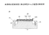
しかしながら、特許文献1に開示された静電チャック装置においても接着剤が侵食される現象を十分に防げていなかった。例えば図1(A)に示すように、絶縁リング14と、静電チャック12との間に隙間15がある場合、プラズマエッチング処理装置などの腐食性の高いプロセスガスを用いた環境下では、該プロセスガスが侵入し、接合層13が侵食されていた。
However, even in the electrostatic chuck device disclosed in Patent Document 1, the phenomenon that the adhesive is eroded has not been sufficiently prevented. For example, as shown in FIG. 1A, when there is a
特にチャンバー内のクリーニングとして定期的に、図1(B)のように静電チャック12上にウェーハ16を保持していない状態、または、ウェーハ16を浮かせた状態でクリーニングが行われる場合がある。この場合、上記の場合よりもさらに隙間15にプロセスガスが侵入しやすくなっており、接合層13が侵食されていた。
In particular, as cleaning in the chamber, cleaning may be performed periodically in a state where the
さらに、特許文献1に開示された静電チャック装置は、静電チャック12の外周部分にさらに絶縁リング14を設けるため、静電チャックの大きさによっては、絶縁リングのサイズも大きくなり、静電チャック装置全体が大型化し、重量も重くなるという問題もあった。
Furthermore, since the electrostatic chuck device disclosed in Patent Document 1 is further provided with an
本発明は、上記従来技術の問題に鑑み、静電チャック装置を大型化することなく、静電チャックと台座部とを接着する接着部が侵食されることをより確実に抑制することができる静電チャック装置を提供することを目的とする。 In view of the above-described problems of the prior art, the present invention is capable of more reliably suppressing the erosion of the bonding portion that bonds the electrostatic chuck and the pedestal portion without increasing the size of the electrostatic chuck device. An object is to provide an electric chuck device.
上記課題を解決するため本発明は、側面を有する台座部と、
前記台座部上に配置され、上面及び側面を有する静電チャックと、
前記台座部と、前記静電チャックとの間に設けられ、前記台座部と前記静電チャックとを接着する樹脂接着剤が配置され、側面を有する接着部と、
前記台座部及び前記静電チャックの側面であって、前記接着部の側面を含む領域に、前記台座部、前記静電チャック、及び前記接着部の外周に沿って設けられ、上端部が前記静電チャックの上面よりも下側に位置する凹部と、
前記凹部に嵌合して設けられ、前記接着部の側面を覆うフォーカスリングと、を有し、
前記凹部は、
前記静電チャックの側面に設けられた下向きの面と、
前記静電チャック、及び前記台座部の側面に設けられた側面と、
前記台座部に設けられた上向きの面と、を有し、
前記接着部の側面は、前記凹部の側面に露出し、
前記フォーカスリングは、前記台座部上に配置され、前記静電チャックの上面の鉛直方向上方から見た場合に前記静電チャックの外周を囲うように構成されていると共に、その内周側が前記凹部に嵌合し、その内周面が前記凹部の側面を覆っている静電チャック装置を提供する。
In order to solve the above problems, the present invention provides a pedestal having side surfaces,
An electrostatic chuck disposed on the pedestal portion and having an upper surface and side surfaces;
A resin adhesive provided between the pedestal portion and the electrostatic chuck, and a resin adhesive that bonds the pedestal portion and the electrostatic chuck is disposed; and an adhesive portion having a side surface;
A side surface of the pedestal portion and the electrostatic chuck is provided along an outer periphery of the pedestal portion, the electrostatic chuck, and the bonding portion in a region including the side surface of the bonding portion, and an upper end portion of the static chuck is fixed to the static chuck. A recess located below the upper surface of the electric chuck;
A focus ring that is fitted to the recess and covers a side surface of the adhesive portion;
The recess is
A downward surface provided on a side surface of the electrostatic chuck;
A side surface provided on a side surface of the electrostatic chuck and the pedestal;
An upward surface provided on the pedestal portion,
The side surface of the adhesive portion is exposed on the side surface of the recess,
The focus ring is disposed on the pedestal portion and is configured to surround the outer periphery of the electrostatic chuck when viewed from above in the vertical direction of the upper surface of the electrostatic chuck, and the inner peripheral side thereof is the recess. The electrostatic chuck device is provided so that the inner peripheral surface covers the side surface of the recess .
本発明によれば、静電チャック装置を大型化することなく、静電チャックと台座部とを接着する接着部が侵食されることをより確実に抑制することができる静電チャック装置を提供することができる。 ADVANTAGE OF THE INVENTION According to this invention, the electrostatic chuck apparatus which can suppress more reliably that the adhesion part which adhere | attaches an electrostatic chuck and a base part is eroded without enlarging an electrostatic chuck apparatus is provided. be able to.
以下に、発明を実施するための形態について図面を用いて説明するが、本発明はこれらの例によって限定されるものではない。 Hereinafter, modes for carrying out the invention will be described with reference to the drawings, but the present invention is not limited to these examples.
本実施形態では本発明の静電チャック装置の構成例について説明する。 In this embodiment, a configuration example of the electrostatic chuck device of the present invention will be described.
本実施形態の静電チャック装置は、台座部と、前記台座部上に配置された静電チャックと、前記台座部と、前記静電チャックとの間に設けられ、前記台座部と前記静電チャックとを接着する樹脂接着剤が配置された接着部と、を有している。そして、前記台座部及び前記静電チャックの側面の、前記接着部を含む領域に、前記台座部及び前記静電チャックの外周に沿って設けられた凹部と、前記凹部に嵌合して設けられ、前記接着部を覆うフォーカスリングを有することを特徴とする。 The electrostatic chuck device of the present embodiment is provided between a pedestal portion, an electrostatic chuck disposed on the pedestal portion, the pedestal portion, and the electrostatic chuck, and the pedestal portion and the electrostatic chuck. And an adhesive portion in which a resin adhesive for adhering the chuck is disposed. A recessed portion provided along an outer periphery of the pedestal portion and the electrostatic chuck is provided in a region of the side surface of the pedestal portion and the electrostatic chuck including the adhesive portion, and is fitted to the recessed portion. And a focus ring that covers the adhesive portion.
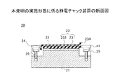
本実施形態の静電チャック装置の断面図を図2に示す。 A sectional view of the electrostatic chuck device of the present embodiment is shown in FIG.
図2に示すように、本実施形態の静電チャック装置20は、台座部21上に、接着部22を介して静電チャック23が配置されている。
As shown in FIG. 2, in the
そして、台座部21及び静電チャック23の側面部分であって、接着部22を含む領域に、台座部21及び静電チャック23の外周に沿って凹部24が形成されている。さらに、該凹部に嵌合し、接着部22(の側面側に露出する面)を覆うようにフォーカスリング25が設けられている。この際、フォーカスリング25は例えば図2に示すようにボルト26により固定することができる。なお、静電チャック23の上面である23Aにウェーハを吸着、保持することができる。
A
ここで、各部材について説明する。 Here, each member will be described.
台座部21の材質は特に限定されるものではないが、静電チャック23を介してウェーハからの熱を伝熱し、ウェーハを冷却する機能を有することから、熱伝導度に優れた材料であることが好ましい。例えば各種金属材料を用いることができ、アルミニウムやステンレス鋼、チタン等を好ましく用いることができる。台座部21の形状は特に限定されるものではないが、通常、静電チャック23は保持するウェーハの形状にあわせて円板形状を有していることから、台座部21についても少なくとも静電チャック23と対向する面については同様の形状を有していることが好ましい。
The material of the
また、台座部21には、ウェーハを冷却するためのガスの供給路や、静電チャック23に電気を供給するための配線、リフトピン設置用の孔等、各種部材を設けることもできる。
The
接着部22には、台座部21と静電チャック23とを接着するための樹脂接着剤が配置されている。該樹脂接着剤の種類については特に限定されるものではないが、例えばシリコーン系、エポキシ系やフェノール系の接着剤を好ましく用いることができる。
A resin adhesive for bonding the
台座部21と、静電チャック23と、を確実に接着するため、図2に示すように台座部21と、静電チャック23との対向する面全体に渡って樹脂接着剤を塗布し、両者が接着されていることが好ましい。
In order to securely bond the
静電チャック23の構造についても特に限定されるものではない。例えば、図2に示すように、電極部231をその内部に含むセラミック基板232を有する構造とすることができる。また、例えば加熱を要する工程に使用する場合にはさらに内部に加熱用のヒーターを含む構成としたり、ウェーハを冷却するためのガスの供給孔や、リフトピン設置用の孔等を設けたりすることもできる。
The structure of the
静電チャック23の形状は例えば保持するウェーハにあわせて円板形状とすることができる。サイズに関しても、特に限定されるものではなく、所望のウェーハを保持できるように選択すればよい。例えば、図2に示すように、保持するウェーハよりも小さいサイズとすることができる。また、保持するウェーハと同じ、または、保持するウェーハよりも大きいサイズでも良い。
The shape of the
凹部24に関しては、上記のように、台座部21及び静電チャック23の側面部分であって、接着部22を含む領域に、台座部21及び静電チャック23の外周に沿って形成されている。係る凹部は、図2に示すように台座部21及び静電チャック23の側面部分に渡って設けられていることが好ましい。このように設けることにより、接着部22を含む広い範囲について、凹部24に嵌合されるフォーカスリング25により覆うことが可能になり、接着部22へのプロセスガスの侵入をより確実に防ぐことができるためである。
As described above, the
また、凹部24は、静電チャック23と台座部21の積層方向(図2中の高さ方向)のうち一部の領域に形成されていることが好ましい。特に、図2に示すように静電チャック23と台座部21の積層方向でみた、凹部24の上端部は、静電チャック23の上面よりも下側にあることが好ましい。また、凹部24の下端部は、台座部21の下面よりも上側にあることが好ましい。
Moreover, it is preferable that the recessed
凹部24の形成方法は特に限定されるものではないが、例えば、台座部21及び静電チャック23のそれぞれに、予め凹部24に対応した形状を形成しておき、両者を接着部22により貼りあわせることより凹部24とすることができる。
The method for forming the
凹部24の形状は特に限定されるものではなく、後述するフォーカスリング25が嵌合するように形成されていればよい。例えば図2に示すように、フォーカスリングの内周面と対向する面が平坦な形状、特に、凹部の断面形状がコの字形状になるように加工することが、凹部加工の容易性の観点から好ましい。なお、上記形状以外にも例えばフォーカスリング25と対向する面に凹部および/または凸部を有する形状とすることもできる。
The shape of the
フォーカスリング25は、凹部24に嵌合し、前記接着部22を覆うように設けられている。フォーカスリング25は、凹部24と同様に、台座部21及び静電チャックの外周に沿って、外周全体に渡って形成され、プロセスガス等の接着部22への侵入を防いでいる。
The
ここで、フォーカスリング25の構成例について図3を用いて説明する。図3(A)がフォーカスリング25の上面図、図3(B)が図3(A)のA−A´線での断面図を示している。
Here, a configuration example of the
フォーカスリング25は、凹部24に嵌合し、接着部22を覆うように形成できれば良く、その形状については特に限定されるものではないが、例えば、図3(A)に示したように環状形状(リング形状)を有していることが好ましい。
The
また、上記のように凹部24の形状としては、その断面形状がコの字形状になるように形成することが好ましいことから、フォーカスリング25についてもこれに対応した形状とすることが好ましい。すなわち、図3(B)に示すようにその内周面が平坦な面、すなわち、凹凸を有していない形状とすることが好ましい。
Further, as described above, since the
図2にもあるようにフォーカスリング25は、台座部21と静電チャック23とを接着した物の側面部に形成された凹部24に設けられているが、係る接着部22を破壊することなくフォーカスリング25を装着、取り外しできるよう構成されていることが好ましい。このため、フォーカスリング25は複数に分割できるように構成されていることが好ましい。具体的には例えば図3(A)に示すように、分割部251において分割できるように構成する、すなわち、その周方向に複数に分割することができることが好ましい。このように構成することにより、台座部21と静電チャック23との接着部22を破壊することなくフォーカスリングを装着、取り外しできるため、フォーカスリング25のみを洗浄したり、交換したりすることができる。
As shown in FIG. 2, the
フォーカスリング25を周方向に複数に分割できるように構成した場合、分割したフォーカスリング25同士を接合する部分、すなわち分割部(接合部)251の形状は特に限定されるものではない。例えば分割したフォーカスリング同士の対向する面に凹凸形状を形成し、互いに噛み合わさるように構成することが好ましい。具体的な構成例を図3(C)に示す。図3(C)は、図3(A)において、ブロック矢印Bの方向から見た分割部(接合部)251の構成例を示している。図3(C)に示すように、分割されたフォーカスリングの対向する面に、互いに噛み合わせるように凹凸を形成することにより、該分割部(接合部)での密着性を高めることができ好ましい。なお、凹凸の形状は特に限定されるものではなく、任意に選択することができる。
In the case where the
凹部24に、フォーカスリング25を嵌合した際に、少なくともフォーカスリング25の内周面と、凹部24のフォーカスリング25の内周面と対向する面との間は隙間がないように形成されていることが好ましい。すなわち、フォーカスリングの内周面と、凹部24のフォーカスリング25の内周面と対向する面とは、対応する形状を有するように形成されていることが好ましい。
When the
また、図2のように、フォーカスリング25の上下の面と、凹部24の上下の面との間についても隙間がないように形成されていることがより好ましい。このように形成することにより、接着部22へのプロセスガス等の侵入をより確実に防ぐことが可能になる。なお、ここでいう隙間がないとは、両者の対向する面が対応する形状を有していることを意味し、加工精度等を考慮した微小な隙間までないことを意味するものではない。
Further, as shown in FIG. 2, it is more preferable that there is no gap between the upper and lower surfaces of the
フォーカスリング25の材料は特に限定されるものではないが、用いるプロセスガスに対して耐食性を有するものであることが好ましい。例えば、シリコン、石英、セラミック材料や、フッ素系樹脂等により好ましく構成することができる。なお、ここでのセラミック材料としては、例えば、Al2O3、Y2O3、MgO、ZrO2等を主成分としたセラミック、又は溶射等によるこれらの被膜形成体を好ましく用いることができる。また、フッ素系樹脂としては、PFAなどを好ましく用いることができる。
The material of the
フォーカスリング25は、図2に示すようにボルト26により、台座部21に固定することができる。図2、図3(B)においては、フォーカスリング25の上面側から、ボルトを挿入し固定する形態を示しているが、係る形態に限定されるものではなく、例えば台座部21の下面側や、フォーカスリング25の側面からボルトを挿入し、固定するように構成することもできる。なお、フォーカスリング25の側面からボルトを挿入する場合には、接着部22とボルトとが離隔して配置されるように、すなわち、接着部22近傍にボルトが配置されないように構成することが好ましい。
The
ボルト26の材料としては特に限定されるものではないが、絶縁材料であることが好ましく、例えば、セラミック材料や樹脂を好ましく用いることができる。樹脂としてはフッ素系樹脂を好ましく用いることができる。また、ボルト26はフォーカスリング25と同じ材料により構成されていることがより好ましい。
The material of the
本実施形態の静電チャック装置においては、上述のように台座部21及び静電チャック23の側面に形成された凹部に嵌合してフォーカスリング25が設けられている。このため、フォーカスリング25の外径は、後述するボルト26を設置する幅の分だけ静電チャック23の外周よりも大きくなる程度であり、静電チャック装置を大型化することなく、接着部22の侵食を防ぐことができる。
In the electrostatic chuck device of the present embodiment, the
上記のように、フォーカスリング25の上面側からボルト26を挿入し、フォーカスリング25を台座部21に固定する場合、図3(B)に示すように、フォーカスリング25に該ボルト26を挿入するためのボルト用の穴252を設けることができる。この場合、係るボルト用の穴内にプロセス中に発生した物質が入ったり、ボルト26がプロセス中に破損したりすることを防止するため、図4に示すように、フォーカスリング25の上部には、上部フォーカスリング41を設けることができる。
As described above, when the
上部フォーカスリング41については上記ボルト用の穴を塞ぐような形状に形成されていればよく、その形状については特に限定されるものではない。例えば、図4に示すように、容易に装着、取り外しができるように、上部フォーカスリング41の内周が、静電チャック23の外周よりも、大きくなるように構成されていることが好ましい。また、装置の大型化を防ぐために、上部フォーカスリング41の外周は、フォーカスリング25の外周と同じ、または、それよりも小さいことが好ましい。
The upper focus ring 41 is not particularly limited as long as the upper focus ring 41 is formed in a shape that closes the hole for the bolt. For example, as shown in FIG. 4, the inner periphery of the upper focus ring 41 is preferably configured to be larger than the outer periphery of the
上部フォーカスリング41の材質については特に限定されるものではないが、フォーカスリング25と同様に、用いるプロセスガスに対して耐食性を有するものであることが好ましく、フォーカスリング25と同じ材料により構成されていることが好ましい。
The material of the upper focus ring 41 is not particularly limited. However, like the
以上、本実施形態の静電チャック装置について説明してきたが、係る静電チャック装置によれば、接着部22がフォーカスリング25に覆われているため、接着部22へのプロセスガス等の侵入をより確実に防ぎ、接着部22の侵食を抑制することが可能になる。また、静電チャック23の外周よりも小径の凹部を形成し、該凹部にフォーカスリング25を設置する形態としているため。静電チャック装置の大型化させることなく、上記効果を得ることができる。
As described above, the electrostatic chuck device according to the present embodiment has been described. However, according to the electrostatic chuck device, since the
20 静電チャック装置
21 台座部
22 接着部
23 静電チャック
24 凹部
25 フォーカスリング
41 上部フォーカスリング
20
Claims (5)
前記台座部上に配置され、上面及び側面を有する静電チャックと、
前記台座部と、前記静電チャックとの間に設けられ、前記台座部と前記静電チャックとを接着する樹脂接着剤が配置され、側面を有する接着部と、
前記台座部及び前記静電チャックの側面であって、前記接着部の側面を含む領域に、前記台座部、前記静電チャック、及び前記接着部の外周に沿って設けられ、上端部が前記静電チャックの上面よりも下側に位置する凹部と、
前記凹部に嵌合して設けられ、前記接着部の側面を覆うフォーカスリングと、を有し、
前記凹部は、
前記静電チャックの側面に設けられた下向きの面と、
前記静電チャック、及び前記台座部の側面に設けられた側面と、
前記台座部に設けられた上向きの面と、を有し、
前記接着部の側面は、前記凹部の側面に露出し、
前記フォーカスリングは、前記台座部上に配置され、前記静電チャックの上面の鉛直方向上方から見た場合に前記静電チャックの外周を囲うように構成されていると共に、その内周側が前記凹部に嵌合し、その内周面が前記凹部の側面を覆っている静電チャック装置。 A pedestal having side surfaces;
An electrostatic chuck disposed on the pedestal portion and having an upper surface and side surfaces;
A resin adhesive provided between the pedestal portion and the electrostatic chuck, and a resin adhesive that bonds the pedestal portion and the electrostatic chuck is disposed; and an adhesive portion having a side surface;
A side surface of the pedestal portion and the electrostatic chuck is provided along an outer periphery of the pedestal portion, the electrostatic chuck, and the bonding portion in a region including the side surface of the bonding portion, and an upper end portion of the static chuck is fixed to the static chuck. A recess located below the upper surface of the electric chuck;
A focus ring that is fitted to the recess and covers a side surface of the adhesive portion;
The recess is
A downward surface provided on a side surface of the electrostatic chuck;
A side surface provided on a side surface of the electrostatic chuck and the pedestal;
An upward surface provided on the pedestal portion,
The side surface of the adhesive portion is exposed on the side surface of the recess,
The focus ring is disposed on the pedestal portion and is configured to surround the outer periphery of the electrostatic chuck when viewed from above in the vertical direction of the upper surface of the electrostatic chuck, and the inner peripheral side thereof is the recess. An electrostatic chuck device that is fitted to the inner surface of the concave portion and covers the side surface of the recess .
前記凹形状の表面が形成された一の部材と、前記凸形状の表面が形成されたもう一方の部材とは、互いに噛み合わさるように構成されている、請求項3に記載の静電チャック装置。 The focus ring member divided into a plurality of members has one member formed with a concave surface and the other member formed with a convex surface facing the concave surface;
The electrostatic chuck device according to claim 3, wherein the one member on which the concave surface is formed and the other member on which the convex surface is formed are configured to mesh with each other. .
Priority Applications (4)
| Application Number | Priority Date | Filing Date | Title |
|---|---|---|---|
| JP2013048185A JP6400273B2 (en) | 2013-03-11 | 2013-03-11 | Electrostatic chuck device |
| TW103105786A TWI606546B (en) | 2013-03-11 | 2014-02-21 | Electrostatic chuck apparatus |
| US14/190,285 US9252039B2 (en) | 2013-03-11 | 2014-02-26 | Electrostatic chuck apparatus |
| KR1020140025410A KR102155122B1 (en) | 2013-03-11 | 2014-03-04 | Electrostatic chuck apparatus |
Applications Claiming Priority (1)
| Application Number | Priority Date | Filing Date | Title |
|---|---|---|---|
| JP2013048185A JP6400273B2 (en) | 2013-03-11 | 2013-03-11 | Electrostatic chuck device |
Publications (3)
| Publication Number | Publication Date |
|---|---|
| JP2014175535A JP2014175535A (en) | 2014-09-22 |
| JP2014175535A5 JP2014175535A5 (en) | 2016-02-18 |
| JP6400273B2 true JP6400273B2 (en) | 2018-10-03 |
Family
ID=51487526
Family Applications (1)
| Application Number | Title | Priority Date | Filing Date |
|---|---|---|---|
| JP2013048185A Active JP6400273B2 (en) | 2013-03-11 | 2013-03-11 | Electrostatic chuck device |
Country Status (4)
| Country | Link |
|---|---|
| US (1) | US9252039B2 (en) |
| JP (1) | JP6400273B2 (en) |
| KR (1) | KR102155122B1 (en) |
| TW (1) | TWI606546B (en) |
Families Citing this family (9)
| Publication number | Priority date | Publication date | Assignee | Title |
|---|---|---|---|---|
| WO2016052291A1 (en) * | 2014-09-30 | 2016-04-07 | 住友大阪セメント株式会社 | Electrostatic chuck device |
| JP6540022B2 (en) * | 2014-12-26 | 2019-07-10 | 東京エレクトロン株式会社 | Mounting table and plasma processing apparatus |
| US10755902B2 (en) * | 2015-05-27 | 2020-08-25 | Tokyo Electron Limited | Plasma processing apparatus and focus ring |
| GB201511282D0 (en) * | 2015-06-26 | 2015-08-12 | Spts Technologies Ltd | Plasma etching apparatus |
| US11024528B2 (en) * | 2015-10-21 | 2021-06-01 | Sumitomo Osaka Cement Co., Ltd. | Electrostatic chuck device having focus ring |
| CN107316795B (en) * | 2016-04-26 | 2020-01-03 | 北京北方华创微电子装备有限公司 | Focusing ring and plasma processing device |
| KR20170127724A (en) * | 2016-05-12 | 2017-11-22 | 삼성전자주식회사 | Plasma processing apparatus |
| JP7228989B2 (en) * | 2018-11-05 | 2023-02-27 | 東京エレクトロン株式会社 | PLACE, EDGE RING POSITIONING METHOD, AND SUBSTRATE PROCESSING APPARATUS |
| CN114843165A (en) * | 2021-02-01 | 2022-08-02 | 中微半导体设备(上海)股份有限公司 | Lower electrode assembly and plasma processing device |
Family Cites Families (13)
| Publication number | Priority date | Publication date | Assignee | Title |
|---|---|---|---|---|
| US6123804A (en) * | 1999-02-22 | 2000-09-26 | Applied Materials, Inc. | Sectional clamp ring |
| US6475336B1 (en) * | 2000-10-06 | 2002-11-05 | Lam Research Corporation | Electrostatically clamped edge ring for plasma processing |
| JP2003179129A (en) * | 2001-12-11 | 2003-06-27 | Ngk Spark Plug Co Ltd | Electrostatic chuck device |
| US7494560B2 (en) * | 2002-11-27 | 2009-02-24 | International Business Machines Corporation | Non-plasma reaction apparatus and method |
| US20040261946A1 (en) * | 2003-04-24 | 2004-12-30 | Tokyo Electron Limited | Plasma processing apparatus, focus ring, and susceptor |
| US7988816B2 (en) * | 2004-06-21 | 2011-08-02 | Tokyo Electron Limited | Plasma processing apparatus and method |
| JP4942471B2 (en) * | 2005-12-22 | 2012-05-30 | 京セラ株式会社 | Susceptor and wafer processing method using the same |
| JP5227197B2 (en) * | 2008-06-19 | 2013-07-03 | 東京エレクトロン株式会社 | Focus ring and plasma processing apparatus |
| US9543181B2 (en) * | 2008-07-30 | 2017-01-10 | Taiwan Semiconductor Manufacturing Company, Ltd. | Replaceable electrostatic chuck sidewall shield |
| JP5100617B2 (en) * | 2008-11-07 | 2012-12-19 | 東京エレクトロン株式会社 | Ring-shaped member and manufacturing method thereof |
| JP5395633B2 (en) * | 2009-11-17 | 2014-01-22 | 東京エレクトロン株式会社 | Substrate mounting table for substrate processing apparatus |
| JP5496630B2 (en) * | 2009-12-10 | 2014-05-21 | 東京エレクトロン株式会社 | Electrostatic chuck device |
| KR20150013627A (en) * | 2012-04-26 | 2015-02-05 | 어플라이드 머티어리얼스, 인코포레이티드 | Methods and apparatus toward preventing esc bonding adhesive erosion |
-
2013
- 2013-03-11 JP JP2013048185A patent/JP6400273B2/en active Active
-
2014
- 2014-02-21 TW TW103105786A patent/TWI606546B/en active
- 2014-02-26 US US14/190,285 patent/US9252039B2/en active Active
- 2014-03-04 KR KR1020140025410A patent/KR102155122B1/en active IP Right Grant
Also Published As
| Publication number | Publication date |
|---|---|
| JP2014175535A (en) | 2014-09-22 |
| KR20140111597A (en) | 2014-09-19 |
| TW201505123A (en) | 2015-02-01 |
| US20140254061A1 (en) | 2014-09-11 |
| US9252039B2 (en) | 2016-02-02 |
| TWI606546B (en) | 2017-11-21 |
| KR102155122B1 (en) | 2020-09-11 |
Similar Documents
| Publication | Publication Date | Title |
|---|---|---|
| JP6400273B2 (en) | Electrostatic chuck device | |
| TWI690014B (en) | Electrostatic chuck device and method for manufacturing electrostatic chuck device | |
| JP5395633B2 (en) | Substrate mounting table for substrate processing apparatus | |
| US10131126B2 (en) | Methods for bonding substrates | |
| TWI653706B (en) | Electrostatic chuck device | |
| JP2015115421A (en) | Plasma processing apparatus and focus ring | |
| KR102604063B1 (en) | Electrostatic chuck assembly and substrate treating apparatus including the assembly | |
| JPWO2019131115A1 (en) | Electrostatic chuck device | |
| KR102474583B1 (en) | Sample holder | |
| JP6506056B2 (en) | Method of manufacturing ceramic member | |
| TWI689037B (en) | Clamp assembly | |
| JP2019087637A (en) | Method of protecting ceramic base material | |
| JP6545613B2 (en) | Focus ring | |
| JP2007258607A (en) | Electrostatic chuck | |
| KR20100095284A (en) | Upper electrode for semiconductor manufacturing device | |
| JP2013042049A (en) | Wafer support device | |
| JP6995016B2 (en) | Sample holder | |
| JP2018509764A (en) | Equipment to improve workpiece temperature uniformity | |
| JP2021100050A (en) | Component fro semiconductor manufacturing device | |
| JP2022124273A (en) | holding member | |
| TWM448795U (en) | Electrostatic chuck provided with DC electrode at edge | |
| KR20130083602A (en) | Assembly of electrostatic chuck |
Legal Events
| Date | Code | Title | Description |
|---|---|---|---|
| A521 | Written amendment |
Free format text: JAPANESE INTERMEDIATE CODE: A523 Effective date: 20151225 |
|
| A621 | Written request for application examination |
Free format text: JAPANESE INTERMEDIATE CODE: A621 Effective date: 20151225 |
|
| A977 | Report on retrieval |
Free format text: JAPANESE INTERMEDIATE CODE: A971007 Effective date: 20161110 |
|
| A131 | Notification of reasons for refusal |
Free format text: JAPANESE INTERMEDIATE CODE: A131 Effective date: 20161115 |
|
| A521 | Written amendment |
Free format text: JAPANESE INTERMEDIATE CODE: A523 Effective date: 20170113 |
|
| A02 | Decision of refusal |
Free format text: JAPANESE INTERMEDIATE CODE: A02 Effective date: 20170328 |
|
| A61 | First payment of annual fees (during grant procedure) |
Free format text: JAPANESE INTERMEDIATE CODE: A61 Effective date: 20180905 |
|
| R150 | Certificate of patent or registration of utility model |
Ref document number: 6400273 Country of ref document: JP Free format text: JAPANESE INTERMEDIATE CODE: R150 |