KR20150013627A - Methods and apparatus toward preventing esc bonding adhesive erosion - Google Patents
Methods and apparatus toward preventing esc bonding adhesive erosion Download PDFInfo
- Publication number
- KR20150013627A KR20150013627A KR1020147033299A KR20147033299A KR20150013627A KR 20150013627 A KR20150013627 A KR 20150013627A KR 1020147033299 A KR1020147033299 A KR 1020147033299A KR 20147033299 A KR20147033299 A KR 20147033299A KR 20150013627 A KR20150013627 A KR 20150013627A
- Authority
- KR
- South Korea
- Prior art keywords
- chuck
- processing chamber
- bonding material
- protective
- electrostatic chuck
- Prior art date
Links
- 238000000034 method Methods 0.000 title claims description 19
- 230000003628 erosive effect Effects 0.000 title claims 2
- 239000000853 adhesive Substances 0.000 title description 4
- 230000001070 adhesive effect Effects 0.000 title description 4
- 239000000463 material Substances 0.000 claims abstract description 79
- 238000012545 processing Methods 0.000 claims abstract description 75
- 230000001681 protective effect Effects 0.000 claims abstract description 55
- 239000000945 filler Substances 0.000 claims abstract description 17
- 238000005260 corrosion Methods 0.000 claims abstract description 9
- 230000007797 corrosion Effects 0.000 claims abstract description 9
- 239000000758 substrate Substances 0.000 claims description 25
- XUIMIQQOPSSXEZ-UHFFFAOYSA-N Silicon Chemical compound [Si] XUIMIQQOPSSXEZ-UHFFFAOYSA-N 0.000 claims description 16
- 229910052710 silicon Inorganic materials 0.000 claims description 16
- 239000010703 silicon Substances 0.000 claims description 16
- 238000012423 maintenance Methods 0.000 abstract description 2
- 239000002245 particle Substances 0.000 description 8
- 230000036961 partial effect Effects 0.000 description 7
- 238000011109 contamination Methods 0.000 description 5
- 238000001816 cooling Methods 0.000 description 4
- 239000007789 gas Substances 0.000 description 4
- 229910052751 metal Inorganic materials 0.000 description 4
- 239000002184 metal Substances 0.000 description 4
- 229920006169 Perfluoroelastomer Polymers 0.000 description 3
- 239000003989 dielectric material Substances 0.000 description 3
- 229920001971 elastomer Polymers 0.000 description 3
- 239000000806 elastomer Substances 0.000 description 3
- 238000005530 etching Methods 0.000 description 3
- 238000010438 heat treatment Methods 0.000 description 3
- 229920000642 polymer Polymers 0.000 description 3
- 239000004065 semiconductor Substances 0.000 description 3
- 239000004696 Poly ether ether ketone Substances 0.000 description 2
- 239000000919 ceramic Substances 0.000 description 2
- 239000002131 composite material Substances 0.000 description 2
- 239000012809 cooling fluid Substances 0.000 description 2
- 229920002530 polyetherether ketone Polymers 0.000 description 2
- 239000000126 substance Substances 0.000 description 2
- 229910018072 Al 2 O 3 Inorganic materials 0.000 description 1
- VYZAMTAEIAYCRO-UHFFFAOYSA-N Chromium Chemical compound [Cr] VYZAMTAEIAYCRO-UHFFFAOYSA-N 0.000 description 1
- 230000002411 adverse Effects 0.000 description 1
- 229910052782 aluminium Inorganic materials 0.000 description 1
- XAGFODPZIPBFFR-UHFFFAOYSA-N aluminium Chemical compound [Al] XAGFODPZIPBFFR-UHFFFAOYSA-N 0.000 description 1
- PNEYBMLMFCGWSK-UHFFFAOYSA-N aluminium oxide Inorganic materials [O-2].[O-2].[O-2].[Al+3].[Al+3] PNEYBMLMFCGWSK-UHFFFAOYSA-N 0.000 description 1
- 238000000231 atomic layer deposition Methods 0.000 description 1
- 230000015572 biosynthetic process Effects 0.000 description 1
- 239000006227 byproduct Substances 0.000 description 1
- 238000005229 chemical vapour deposition Methods 0.000 description 1
- 229910052804 chromium Inorganic materials 0.000 description 1
- 239000011651 chromium Substances 0.000 description 1
- 238000004891 communication Methods 0.000 description 1
- 239000004020 conductor Substances 0.000 description 1
- 230000008878 coupling Effects 0.000 description 1
- 238000010168 coupling process Methods 0.000 description 1
- 238000005859 coupling reaction Methods 0.000 description 1
- 238000000151 deposition Methods 0.000 description 1
- 230000008021 deposition Effects 0.000 description 1
- 238000001312 dry etching Methods 0.000 description 1
- 230000000694 effects Effects 0.000 description 1
- 238000010292 electrical insulation Methods 0.000 description 1
- 239000012530 fluid Substances 0.000 description 1
- 239000011521 glass Substances 0.000 description 1
- 230000003993 interaction Effects 0.000 description 1
- 238000005468 ion implantation Methods 0.000 description 1
- 238000002955 isolation Methods 0.000 description 1
- 230000000670 limiting effect Effects 0.000 description 1
- 239000007788 liquid Substances 0.000 description 1
- 239000004973 liquid crystal related substance Substances 0.000 description 1
- TWNQGVIAIRXVLR-UHFFFAOYSA-N oxo(oxoalumanyloxy)alumane Chemical compound O=[Al]O[Al]=O TWNQGVIAIRXVLR-UHFFFAOYSA-N 0.000 description 1
- 230000000149 penetrating effect Effects 0.000 description 1
- -1 perfluoro Chemical group 0.000 description 1
- 229920003223 poly(pyromellitimide-1,4-diphenyl ether) Polymers 0.000 description 1
- 229920001296 polysiloxane Polymers 0.000 description 1
- 239000002243 precursor Substances 0.000 description 1
- 238000012546 transfer Methods 0.000 description 1
Images


Classifications
-
- H—ELECTRICITY
- H01—ELECTRIC ELEMENTS
- H01L—SEMICONDUCTOR DEVICES NOT COVERED BY CLASS H10
- H01L21/00—Processes or apparatus adapted for the manufacture or treatment of semiconductor or solid state devices or of parts thereof
- H01L21/67—Apparatus specially adapted for handling semiconductor or electric solid state devices during manufacture or treatment thereof; Apparatus specially adapted for handling wafers during manufacture or treatment of semiconductor or electric solid state devices or components ; Apparatus not specifically provided for elsewhere
- H01L21/683—Apparatus specially adapted for handling semiconductor or electric solid state devices during manufacture or treatment thereof; Apparatus specially adapted for handling wafers during manufacture or treatment of semiconductor or electric solid state devices or components ; Apparatus not specifically provided for elsewhere for supporting or gripping
- H01L21/6831—Apparatus specially adapted for handling semiconductor or electric solid state devices during manufacture or treatment thereof; Apparatus specially adapted for handling wafers during manufacture or treatment of semiconductor or electric solid state devices or components ; Apparatus not specifically provided for elsewhere for supporting or gripping using electrostatic chucks
- H01L21/6833—Details of electrostatic chucks
-
- B—PERFORMING OPERATIONS; TRANSPORTING
- B32—LAYERED PRODUCTS
- B32B—LAYERED PRODUCTS, i.e. PRODUCTS BUILT-UP OF STRATA OF FLAT OR NON-FLAT, e.g. CELLULAR OR HONEYCOMB, FORM
- B32B7/00—Layered products characterised by the relation between layers; Layered products characterised by the relative orientation of features between layers, or by the relative values of a measurable parameter between layers, i.e. products comprising layers having different physical, chemical or physicochemical properties; Layered products characterised by the interconnection of layers
- B32B7/04—Interconnection of layers
- B32B7/12—Interconnection of layers using interposed adhesives or interposed materials with bonding properties
-
- B—PERFORMING OPERATIONS; TRANSPORTING
- B32—LAYERED PRODUCTS
- B32B—LAYERED PRODUCTS, i.e. PRODUCTS BUILT-UP OF STRATA OF FLAT OR NON-FLAT, e.g. CELLULAR OR HONEYCOMB, FORM
- B32B3/00—Layered products comprising a layer with external or internal discontinuities or unevennesses, or a layer of non-planar form; Layered products having particular features of form
- B32B3/02—Layered products comprising a layer with external or internal discontinuities or unevennesses, or a layer of non-planar form; Layered products having particular features of form characterised by features of form at particular places, e.g. in edge regions
- B32B3/04—Layered products comprising a layer with external or internal discontinuities or unevennesses, or a layer of non-planar form; Layered products having particular features of form characterised by features of form at particular places, e.g. in edge regions characterised by at least one layer folded at the edge, e.g. over another layer ; characterised by at least one layer enveloping or enclosing a material
-
- B—PERFORMING OPERATIONS; TRANSPORTING
- B32—LAYERED PRODUCTS
- B32B—LAYERED PRODUCTS, i.e. PRODUCTS BUILT-UP OF STRATA OF FLAT OR NON-FLAT, e.g. CELLULAR OR HONEYCOMB, FORM
- B32B3/00—Layered products comprising a layer with external or internal discontinuities or unevennesses, or a layer of non-planar form; Layered products having particular features of form
- B32B3/02—Layered products comprising a layer with external or internal discontinuities or unevennesses, or a layer of non-planar form; Layered products having particular features of form characterised by features of form at particular places, e.g. in edge regions
- B32B3/08—Layered products comprising a layer with external or internal discontinuities or unevennesses, or a layer of non-planar form; Layered products having particular features of form characterised by features of form at particular places, e.g. in edge regions characterised by added members at particular parts
-
- H—ELECTRICITY
- H01—ELECTRIC ELEMENTS
- H01J—ELECTRIC DISCHARGE TUBES OR DISCHARGE LAMPS
- H01J37/00—Discharge tubes with provision for introducing objects or material to be exposed to the discharge, e.g. for the purpose of examination or processing thereof
- H01J37/32—Gas-filled discharge tubes
- H01J37/32431—Constructional details of the reactor
- H01J37/32715—Workpiece holder
-
- Y—GENERAL TAGGING OF NEW TECHNOLOGICAL DEVELOPMENTS; GENERAL TAGGING OF CROSS-SECTIONAL TECHNOLOGIES SPANNING OVER SEVERAL SECTIONS OF THE IPC; TECHNICAL SUBJECTS COVERED BY FORMER USPC CROSS-REFERENCE ART COLLECTIONS [XRACs] AND DIGESTS
- Y10—TECHNICAL SUBJECTS COVERED BY FORMER USPC
- Y10T—TECHNICAL SUBJECTS COVERED BY FORMER US CLASSIFICATION
- Y10T428/00—Stock material or miscellaneous articles
- Y10T428/23—Sheet including cover or casing
- Y10T428/239—Complete cover or casing
-
- Y—GENERAL TAGGING OF NEW TECHNOLOGICAL DEVELOPMENTS; GENERAL TAGGING OF CROSS-SECTIONAL TECHNOLOGIES SPANNING OVER SEVERAL SECTIONS OF THE IPC; TECHNICAL SUBJECTS COVERED BY FORMER USPC CROSS-REFERENCE ART COLLECTIONS [XRACs] AND DIGESTS
- Y10—TECHNICAL SUBJECTS COVERED BY FORMER USPC
- Y10T—TECHNICAL SUBJECTS COVERED BY FORMER US CLASSIFICATION
- Y10T428/00—Stock material or miscellaneous articles
- Y10T428/31504—Composite [nonstructural laminate]
Abstract
본 발명의 실시예들은, 프로세싱 환경에서 프로세싱 환경들로부터 본딩 재료를 차폐(shielding)하기 위한 보호 엘리먼트를 갖는 챔버 컴포넌트들을 제공한다. 보호 엘리먼트는, 보호 시일(seal)들, 보호 구조들, 부식 저항성 충전제들, 또는 이들의 조합들을 포함할 수 있다. 본 발명의 실시예들은, 프로세싱 챔버에서 사용되는 본딩 재료의 부식을 감소시키고, 따라서, 프로세싱 품질을 개선하며 유지보수 비용을 감소시킨다.Embodiments of the present invention provide chamber components having a protection element for shielding bonding material from processing environments in a processing environment. The protective element may comprise protective seals, protective structures, corrosion resistant fillers, or combinations thereof. Embodiments of the present invention reduce corrosion of the bonding material used in the processing chamber, thus improving processing quality and reducing maintenance costs.

Description
본 발명의 실시예들은, 열적 및/또는 화학적 안정성들이 향상된, 본딩(bonding) 재료들에 의해 접합된 복합 구조(composite structure)들에 관한 것이다. 특히, 본 발명의 실시예들은, 본딩 재료에 의해 접합된 2개 또는 그 초과의 컴포넌트들을 갖는 정전 척에 관한 것이다.Embodiments of the present invention relate to composite structures bonded by bonding materials with improved thermal and / or chemical stability. In particular, embodiments of the present invention relate to an electrostatic chuck having two or more components joined together by a bonding material.
반도체 프로세싱 챔버들은 종종, 원하는 특성들을 달성하기 위해 본딩 재료들로 2개 또는 그 초과의 컴포넌트들을 함께 본딩함으로써 형성된 파트(part)들을 포함한다. 예컨대, 프로세싱 동안에 기판들을 지지하고 고정시키기 위해 사용되는 정전 척들은 일반적으로, 열 전도성 본딩 재료에 의해 금속성 베이스에 본딩된 유전체 퍽(puck)을 포함한다. 본딩 재료들은, 열 전도성 및/또는 전기 절연을 제공하면서, 상이한 컴포넌트들 사이의 고정된(secured) 연결을 제공한다. 그러나, 본딩 재료들은, 특히 높은 온도들에서 또는 해시 케미컬(hash chemical) 환경에서 프로세스들이 수행되는 경우에, 프로세싱에 대해 악영향을 미칠 수 있다. 예컨대, 플라즈마에 대해 노출되는 경우에, 정전 척에서의 본딩 재료는 부식될 수 있고, 프로세싱 챔버에서의 입자 오염을 야기하는 입자들을 생성할 수 있다.Semiconductor processing chambers often include parts formed by bonding together two or more components together with bonding materials to achieve desired properties. For example, electrostatic chucks used to support and hold substrates during processing typically include a dielectric puck bonded to a metallic base by a thermally conductive bonding material. The bonding materials provide a secure connection between different components, while providing thermal conductivity and / or electrical insulation. However, bonding materials can have an adverse effect on processing, especially when processes are performed at high temperatures or in a hash chemical environment. For example, when exposed to a plasma, the bonding material in the electrostatic chuck can corrode and create particles that cause particle contamination in the processing chamber.
본 발명의 실시예들은, 본딩 재료 부식 및 입자 생성을 방지하기 위한 장치 및 방법들을 제공한다.Embodiments of the present invention provide apparatus and methods for preventing bonding material corrosion and particle generation.
본 발명의 실시예들은, 프로세싱 환경에서 프로세싱 환경들로부터, 정전 척과 같은 챔버 컴포넌트들을 접합시키는 것에서 사용되는 본딩 재료를 보호하기 위한 장치 및 방법들을 제공한다.Embodiments of the present invention provide apparatus and methods for protecting bonding materials used in bonding chamber components, such as electrostatic chucks, from processing environments in a processing environment.
본 발명의 일 실시예는 프로세싱 챔버에서 사용하기 위한 장치를 제공한다. 장치는, 제 1 컴포넌트, 제 2 컴포넌트, 및 제 1 컴포넌트와 제 2 컴포넌트를 접합시키는 본딩 재료를 포함한다. 장치는, 프로세싱 챔버에서 본딩 재료가 부식되는 것을 방지하기 위한 보호 엘리먼트를 더 포함한다.One embodiment of the present invention provides an apparatus for use in a processing chamber. The apparatus includes a first component, a second component, and a bonding material for bonding the first component and the second component. The apparatus further includes a protective element for preventing the bonding material from corroding in the processing chamber.
본 발명의 다른 실시예는 프로세싱 챔버를 위한 정전 척을 제공한다. 정전 척은, 기판을 위에 지지하도록 구성된 상부 표면 및 상부 표면과 대향하는(opposing) 하부 표면을 갖는 척 바디(body), 척 바디의 하부 표면과 대면하는(facing) 상부 표면을 갖는 척 베이스, 및 척 베이스의 상부 표면과 척 바디의 하부 표면을 접합시키는 본딩 재료를 포함한다. 정전 척은, 프로세싱 챔버에서의 환경에 의해 본딩 재료가 부식되는 것을 방지하기 위한 보호 엘리먼트를 더 포함한다.Another embodiment of the present invention provides an electrostatic chuck for a processing chamber. The electrostatic chuck comprises a chuck body having a top surface configured to support a substrate thereon and an opposing bottom surface opposing the top surface, a chuck base having a top surface facing a bottom surface of the chuck body, And a bonding material for bonding the upper surface of the chuck base and the lower surface of the chuck body. The electrostatic chuck further includes a protective element for preventing the bonding material from being corroded by the environment in the processing chamber.
본 발명의 상기 열거된 특징들이 상세히 이해될 수 있는 방식으로 앞서 간략히 요약된 본 발명의 보다 구체적인 설명이 실시예들을 참조로 하여 이루어질 수 있는데, 이러한 실시예들의 일부는 첨부된 도면들에 예시되어 있다. 그러나, 첨부된 도면들은 본 발명의 단지 전형적인 실시예들을 도시하는 것이므로 본 발명의 범위를 제한하는 것으로 간주되지 않아야 한다는 것이 주목되어야 하는데, 이는 본 발명이 다른 균등하게 유효한 실시예들을 허용할 수 있기 때문이다.
도 1a는 본 발명의 일 실시예에 따른, 보호 시일들을 갖는 정전 척의 개략적인 측면도이다.
도 1b는 도 1a의 정전 척의 확대된 부분적인 단면도이다.
도 1c는 본 발명의 다른 실시예에 따른, 정전 척의 확대된 부분적인 단면도이다.
도 1d는 본 발명의 다른 실시예에 따른, 정전 척의 확대된 부분적인 단면도이다.
도 1e는 척 바디가 제거된, 도 1a의 정전 척의 상면도이다.
도 2a는 본 발명의 일 실시예에 따른, 보호 구조를 갖는 정전 척의 측단면도이다.
도 2b는 본 발명의 다른 실시예에 따른, 보호 구조를 갖는 정전 척의 확대된 부분적인 단면도이다.
도 2c는 본 발명의 다른 실시예에 따른, 보호 구조를 갖는 정전 척의 확대된 부분적인 단면도이다.
도 3은 본 발명의 실시예들에 따른, 정전 척을 갖는 플라즈마 프로세싱 챔버의 측단면도이다.
이해를 용이하게 하기 위하여, 도면들에 대해 공통인 동일한 엘리먼트들을 지시하기 위해 가능한 경우에 동일한 참조 번호들이 사용되었다. 또한, 일 실시예의 엘리먼트들 및 특징들이 추가적인 설명 없이 다른 실시예들 상에 유익하게 포함될 수 있다는 것이 고려된다.A more particular description of the invention, briefly summarized above, may be had by reference to the embodiments, in which the recited features of the invention can be understood in detail, some of which are illustrated in the accompanying drawings . It should be noted, however, that the appended drawings illustrate only typical embodiments of this invention and are therefore not to be considered limiting of its scope, for the invention may admit to other equally effective embodiments to be.
FIG. 1A is a schematic side view of an electrostatic chuck having protective seals, in accordance with an embodiment of the present invention. FIG.
1B is an enlarged partial cross-sectional view of the electrostatic chuck of FIG. 1A.
1C is an enlarged partial cross-sectional view of an electrostatic chuck, according to another embodiment of the present invention.
1D is an enlarged partial cross-sectional view of an electrostatic chuck, according to another embodiment of the present invention.
1E is a top view of the electrostatic chuck of FIG. 1A with the chuck body removed.
2A is a side cross-sectional view of an electrostatic chuck having a protection structure according to an embodiment of the present invention.
2B is an enlarged partial cross-sectional view of an electrostatic chuck having a protection structure, according to another embodiment of the present invention.
2C is an enlarged partial cross-sectional view of an electrostatic chuck having a protective structure, according to another embodiment of the present invention.
3 is a side cross-sectional view of a plasma processing chamber having an electrostatic chuck, in accordance with embodiments of the present invention.
To facilitate understanding, identical reference numerals have been used, where possible, to designate identical elements that are common to the figures. It is also contemplated that the elements and features of one embodiment may be beneficially included on other embodiments without further description.
본 발명의 실시예들은, 프로세싱 환경에서 프로세싱 환경들로부터, 정전 척과 같은 챔버 컴포넌트들을 접합시키는 것에서 사용되는 본딩 재료를 보호하기 위한 장치 및 방법들을 제공한다. 일 실시예에서, 프로세싱 환경에 대한 노출로부터 본딩 재료의 에지를 둘러싸도록 보호 시일이 배치된다. 다른 실시예에서, 프로세싱 환경에 대한 본딩 재료의 직접적인 노출을 방지하기 위해, 챔버 컴포넌트에서의 본딩 재료 주위에 보호 구조가 형성된다. 본 발명의 다른 실시예에 따르면, 규소 충전제 및 폴리머 접착제 베이스를 포함하는 본딩 재료가, 입자 생성을 감소시키면서 챔버 컴포넌트들을 접합시키는 것에서 사용된다. 본 발명의 실시예들은, 프로세싱 챔버에서 사용되는 본딩 재료의 부식을 감소시키고, 따라서, 프로세싱 품질을 개선하고 유지보수 비용을 감소시킨다.Embodiments of the present invention provide apparatus and methods for protecting bonding materials used in bonding chamber components, such as electrostatic chucks, from processing environments in a processing environment. In one embodiment, a protective seal is disposed to surround the edge of the bonding material from exposure to the processing environment. In another embodiment, a protective structure is formed around the bonding material in the chamber component to prevent direct exposure of the bonding material to the processing environment. According to another embodiment of the present invention, a bonding material comprising a silicon filler and a polymeric adhesive base is used in bonding chamber components while reducing grain formation. Embodiments of the present invention reduce corrosion of the bonding material used in the processing chamber, thus improving processing quality and reducing maintenance costs.
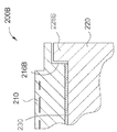
도 1a는 본 발명의 일 실시예에 따른 정전 척(100)의 측단면도이다. 정전 척(100)은 프로세싱 동안에 기판을 지지하기 위해 기판 프로세싱 챔버에 이동가능하게 또는 고정적으로 위치될 수 있다. 정전 척(100)은 본딩 재료(130)에 의해 척 베이스(120)에 고정된 척 바디(110)를 포함한다. 프로세싱 환경으로부터 본딩 재료(130)를 보호하기 위해, 본딩 재료(130) 주위에 보호 시일(140)이 배치된다.1A is a side cross-sectional view of an
척 바디(110)는, 기판(102)을 위에 지지하기 위한 실질적으로 평탄한 상부 표면(112)을 갖는다. 척 바디(110)는 또한, 본딩 재료(130)를 수용하고 척 베이스(120)에 커플링하기 위한 실질적으로 평탄한 하부 표면(114)을 갖는다. 척 바디(110)는 유전체 재료로 형성될 수 있다. 일 실시예에서, 척 바디(110)는 알루미늄 산화물과 같은 세라믹으로 형성될 수 있다. 척 바디(110)에 전극(118)이 매립될 수 있다. 전극(118)은 얇은 금속 플레이트 또는 금속 메시(mesh)일 수 있다. 전극(118)은 실질적으로 기판(102)의 전체 영역을 에워싸기에 충분하게 클 수 있다. 전극(118)은, 기판(120)을 상부 표면(112)으로 끌어당기고 상부 표면(112) 상에 고정시키기 위한 정전 척킹력(electrostatic chucking force)을 생성하기 위해, DC 전압 소스와 같은 전력 소스에 커플링될 수 있다. 선택적으로, 전극(118)은 또한, 프로세싱 챔버에서 용량성 커플링된 플라즈마를 생성하기 위해 RF 전력 소스에 커플링될 수 있다.The
척 바디(110)는, 리프트 핀들(104)이 통과하게 허용하기 위한 3개 또는 그 초과의 관통 홀(through hole)들(116)을 가질 수 있다. 척 바디(110)는, 프로세싱되는 기판(102)의 형상에 따라 형성될 수 있다. 예컨대, 척 바디(110)는 반도체 기판과 같은 원형 기판을 지지하기 위한 원형 디스크일 수 있다. 척 바디(110)는 또한, 액정 디스플레이 디바이스들을 형성하기 위한 유리 기판들과 같은 직사각형 기판들을 지지하기 위한 직사각형 플레이트일 수 있다.The
척 베이스(120)는, 본딩 재료(130) 및 척 바디(110)를 수용하기 위한 상부 표면(122)을 갖는다. 상부 표면(122)은 실질적으로 평탄할 수 있다. 척 베이스(120)는, 척 바디(110)에 대해 온도 제어를 제공하기 위해, 금속과 같은 열 전도성 재료로 형성될 수 있다. 일 실시예에서, 척 베이스(120)는 알루미늄으로 형성된다. 척 베이스(120)는, 그 내부에 형성된 냉각 채널들(123)을 가질 수 있다. 냉각 채널들(123)은 냉각 유체 소스(미도시)에 연결될 수 있고, 그 냉각 채널들(123) 내부에서 순환되는 냉각 유체를 가질 수 있다. 척 베이스(120)는 또한, 척 바디(110)에 대해 가열을 제공하기 위해 그 내부에 형성된 하나 또는 그 초과의 가열 엘리먼트들(124)을 가질 수 있다. 척 베이스(120)는, 그 척 베이스(120)를 통해 형성되고 리프트 핀들(104)을 수용하기 위해 척 바디(110)에서의 관통 홀들(116)과 정렬되는 리프트 핀 개구들(126)을 가질 수 있다. 일 실시예에서, 케이싱 엘리먼트들(132, 134, 138)이, 리프트 핀들(104)을 가이딩하기 위해 리프트 핀 개구들(126)에 배치될 수 있다. 케이싱 엘리먼트들(132, 134, 138)은, 척 베이스(120)와 리프트 핀들(104) 사이의 전기적인 격리를 제공하기 위해 VESPEL® 폴리머 또는 폴리에테르 에테르 케톤(PEEK)과 같은 유전체 재료로 형성될 수 있다.The
본딩 재료(130)는, 척 바디(110)와 척 베이스(120)를 함께 접합시키기 위해 척 베이스(120)의 상부 표면(122)과 척 바디(110)의 하부 표면(114) 사이에 배치된다. 본딩 재료(130)는 척 베이스(120) 및 척 바디(110)와 유사하게 형성된 시트(sheet)의 형태일 수 있다. 일 실시예에서, 본딩 재료(130)의 시트는, 리프트 핀들(104)을 위한 관통 홀들(116)에 대응하는 3개 또는 그 초과의 리프트 핀 홀들(136)을 포함할 수 있다. 대안적으로, 본딩 재료(130)는 액체 기반일 수 있다.The
본딩 재료(130)는 금속성 척 베이스(120)와 세라믹 척 바디(110)와 같은 유사하지 않은 재료들 사이에 단단한 접합을 제공하도록 구성된다. 본딩 재료(130)는 또한, 접합된 컴포넌트들 사이에 열 전도를 제공한다. 일 실시예에서, 본딩 재료(130)는, 열 전도성을 제공하기 위한 충전제 재료들을 갖는 폴리머 기반 본딩 접착제일 수 있다. 본딩 재료(130)는 부식 저항성 충전제들을 갖는 폴리머 기반 본딩 접착제일 수 있다. 일 실시예에서, 충전제 재료는 규소를 포함하고, 폴리머 베이스 재료는 실리콘(Silicone)을 포함한다. 실리콘 베이스에서의 충전제 재료의 농도는 1 W/mK의 열 전도성을 달성하도록 제어된다.The
통상적인(conventional) 본딩 재료에서의 충전제들은, O2와 NF3 또는 NF3를 포함하는 프로세싱 환경과 같은 에칭 케미스트리(etching chemistry)에서 부식될 수 있어서, 백색 입자(white particle)들이 생성될 수 있고 오염이 야기될 수 있다. 종래의(traditional) 충전제들을 갖는 본딩 재료들과 비교하면, 실리콘 베이스 및 규소 충전제를 갖는 본딩 재료(130)는 O2와 NF3 또는 NF3를 포함하는 프로세싱 케미스트리에서 입자 오염을 야기하지 않고, 따라서, 입자 오염을 크게 감소시킨다. 예컨대, NF3 케미스트리에서, 베이스 폴리머 실리콘이 공격을 받고, 실리콘이 휘발되어, 알루미나(Al2O3) 충전제들과 같은 종래의 충전제들이 남게 되면서, 입자 문제들이 야기된다. 규소 충전제들이 사용되는 경우에, 규소 충전제 및 실리콘 베이스 양자 모두가, 어떠한 입자들도 생성하지 않으면서, NF3 공격 하에서 휘발된다. 규소 충전제들을 포함하는 본딩 재료(130)는 보호 시일(140)과 조합하여, 또는 단독으로 사용될 수 있다.Fillers in conventional bonding materials can be corroded in etching chemistries, such as in a processing environment that includes O 2 and NF 3 or NF 3 , so that white particles can be created Contamination can be caused. Compared to bonding materials with traditional fillers, the
일 실시예에서, 보호 시일(140)은 프로세싱 환경과 본딩 재료(130) 사이의 상호작용을 방지하기 위해 본딩 재료(130)를 한정(circumscribe)한다. 일 실시예에서, 보호 시일(140)을 제 위치에 홀딩하기 위해 척 베이스(120)와 척 바디(110) 사이에 리세스(144)가 형성될 수 있다. 선택적으로, 본딩 재료(130)가 리프트 핀 홀들(136)에서의 환경에 대해 노출되는 것을 방지하기 위해, 본딩 재료(130)에서의 각각의 리프트 핀 홀들(136) 주위에 보호 시일(142)이 배치될 수 있다.In one embodiment, the
보호 시일들(140, 142)은, 프로세싱 환경에 대해 노출되는 경우에 척 베이스(120)와 척 바디(110) 사이에 시일을 유지하는 재료들로 형성될 수 있다. 보호 시일들(140, 142)은, 퍼플루오로엘라스토머(perfluoroelastomer)와 같은 엘라스토머로 형성될 수 있다. O2와 NF3 또는 NF3를 포함하는 에칭 케미스트리에서 동작하기 위해, 보호 시일들(140, 142)은, KALREZ® 8575 퍼플루오로엘라스토머, DUPRA® 192 퍼플루오로엘라스토머, KALREZ® 8085 퍼플루오로엘라스토머, CHEMRAZ® XPE 엘라스토머 중 하나(그러나 이에 제한되지는 않음)에 의해 형성될 수 있다. L7505, SC513(Chemraz 513), L8015r1, G758(Perlast), L8010과 같은 다른 재료들이 또한 보호 시일들에 대해 적합하다. 보호 시일들(140, 142)은 O-링, 개스킷, 컵 시일의 형태일 수 있거나, 또는 다른 적합한 프로파일을 가질 수 있다. 보호 시일들(140, 142)은 선택적으로, 스프링 로딩될 수 있다.The
도 1b에서 도시된 바와 같이, 정전 척(100)에서의 리세스(144)는, 척 바디(110)의 하부 표면(114)과 척 베이스(120)에 형성된 스텝에 의해 정의될 수 있다. 척 베이스(120)만이 리세스(144)를 형성하도록 머시닝되기(machined) 때문에, 이러한 구성은 구현하기 쉽다. 도 1e는, 척 바디(110)가 제거되어 보호 시일들(140, 142)을 볼 수 있는, 정전 척(100)의 척 베이스(120)의 상면도이다.1B, the
대안적으로, 보호 시일(140)을 위한 리세스는, 척 바디(110)와 척 베이스(120) 양자 모두에, 또는 척 바디(110) 상에만 형성될 수 있다.Alternatively, the recess for the
도 1c는 본 발명의 다른 실시예에 따른, 정전 척(100C)의 확대된 부분적인 단면도이다. 정전 척(100C)은, 척 베이스(120)의 상부 표면(122) 상에 형성된 스텝(128C) 및 척 바디(110)의 하부 표면(114) 상에 형성된 스텝(115C)에 의해 정의된 리세스(144C)에 보호 시일(140)이 고정된 것을 제외하면, 도 1a의 정전 척(100)과 유사하다. 이러한 구성은, 본딩 재료(130)가 보호 시일(140)의 중간 부분에 의해 덮이는 것을 보장한다.1C is an enlarged partial cross-sectional view of an electrostatic chuck 100C, according to another embodiment of the present invention. The electrostatic chuck 100C includes a recess 128C defined by a step 128C formed on the
도 1d는 본 발명의 다른 실시예에 따른 정전 척(100D)의 확대된 부분적인 단면도이다. 정전 척(100D)은, 척 베이스(120)의 상부 표면(122) 및 척 바디(110)의 하부 표면(114) 상에 형성된 스텝(115D)에 의해 정의된 리세스(144D)에 보호 시일(140)이 고정된 것을 제외하면, 도 1a의 정전 척(100)과 유사하다. 척 바디(110)만이 리세스(144d)를 형성하도록 머시닝된다.1D is an enlarged partial cross-sectional view of an
본딩 재료들에 대한 부식을 방지하기 위해 보호 시일을 사용하는 것에 부가하여, 또는 그에 대해 대안적으로, 본 발명의 실시예들은 또한, 본딩 재료들을 보호하기 위해 척 베이스 및/또는 척 바디 내에 차폐(shielding) 피쳐들을 갖는 정전 척들을 제공한다.In addition to, or as an alternative to, the use of protective seals to prevent corrosion on the bonding materials, embodiments of the present invention may also include shielding in the chuck base and / or the chuck body to protect the bonding materials shielding < / RTI > features.
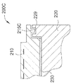
도 2a는 본 발명의 일 실시예에 따른, 본딩 재료 보호 구조, 즉, 차폐 피쳐를 갖는 정전 척(200)의 측단면도이다. 정전 척(200)은, 프로세싱 동안에 기판을 지지하기 위해 기판 프로세싱 챔버에서 이동가능하게 또는 고정적으로 위치될 수 있다. 정전 척(100)과 유사하게, 정전 척(200)은, 본딩 재료(130)와 동일한 본딩 재료(230)에 의해 척 베이스(220)에 고정된 척 바디(210)를 포함한다. 보호 구조(216)는, 프로세싱 환경으로부터 본딩 재료(230)를 차폐하기 위해 척 베이스(220) 및/또는 척 바디(210)에 형성될 수 있다.2A is a side cross-sectional view of an
척 바디(210)는, 기판(102)을 위에 지지하기 위한 상부 표면(212), 및 본딩 재료(230)를 수용하기 위한 실질적으로 평탄한 하부 표면(214)을 갖는다. 척 바디(210)는 유전체 재료로 형성될 수 있다. 척 바디(210)에 전극(218)이 매립될 수 있다.The
척 베이스(220)는 척 바디(210) 및 본딩 재료(230)를 수용하기 위한 상부 표면(222)을 갖는다. 척 베이스(220)는, 온도 제어를 위해 내부에 매립된 가열 엘리먼트들(224) 및 내부에 형성된 냉각 채널들(223)을 가질 수 있다.The
본딩 재료(230)는, 척 바디(210)와 척 베이스(220)를 함께 접합시키기 위해, 척 베이스(220)의 상부 표면(222)과 척 바디(210)의 하부 표면(214) 사이에 배치된다. 척 바디(210)의 하부 표면(214) 및 척 베이스(220)의 상부 표면(222)은, 척 베이스(220) 및/또는 척 바디(210)에 의해 형성된 보호 구조(216)에 의해 본딩 재료(230)가 둘러싸일 수 있도록, 척 베이스(220) 및 척 바디(210)의 외측 에지들보다 더 작을 수 있다.The
도 2a에서 도시된 실시예에 따르면, 척 베이스(220)는, 상부 표면(222)으로부터 아래로 강하된 스텝(228)을 갖는다. 보호 구조(216)는, 척 바디(210)의 하부 표면(214)으로부터 하방으로 연장되는 립(lip)의 형태이다. 립은 연속적일 수 있다. 척 바디(210)가 척 베이스(220)에 고정되는 경우에, 립(216)의 형태인 보호 구조(216)는 스텝(228) 위로 연장되고, 척 베이스(220)의 상부 표면과 척 바디(210)의 하부 표면(214) 사이의 인터페이스를 덮으며, 따라서, 본딩 재료(230)를 측면에서(laterally) 둘러싸고, 챔버 내의 환경에 대한 가시선(line of sight) 노출로부터 본딩 재료(230)를 차폐한다. 보호 시일을 사용하지 않으면서, 정전 척(200)의 보호 구조(216)는, 보호 시일들을 유지하고 교체하기 위한 필요성들을 제거하고, 따라서, 동작 비용을 감소시킨다. 일 실시예에서, 본딩 재료(230)가 프로세싱 환경에 대해 노출되는 것을 방지하기 위해, 각각의 리프트 핀 통로들(219) 주위에 연속적인 립(217)이 또한 형성될 수 있다.According to the embodiment shown in FIG. 2A, the
도 2a에서 보호 구조(216)가 척 바디(210)로부터의 립의 형태로 도시되어 있지만, 임의의 적합한 구조들이 본딩 재료(230)를 차폐하기 위해 사용될 수 있다. 예컨대, 도 2b는, 척 베이스(220)로부터 상방으로 연장되고 척 바디(210)의 외측 에지(216B)를 둘러싸는 보호 립(228B)의 형태의 보호 구조를 갖는 정전 척(200B)의 확대된 부분적인 단면도이다. 도 2c에서 도시된 정전 척(200C)에서, 척 베이스(220)는, 척 바디(210)로부터의 립(215C)을 수용하도록 구성된 그루브(groove)(229)를 갖는다. 그루브(229) 및 립(215C)은, 정전 척(200C)을 둘러싸는 프로세싱 환경으로부터 본딩 재료(230)를 격리시키기 위한 미로(maze)를 형성한다.Although the
본 발명의 실시예들에 따르면, 보호 시일들, 보호 구조들, 또는 부식 저항성 충전제들과 같은 하나 또는 그 초과의 보호 엘리먼트들이, 프로세싱 환경에서 본딩 재료가 부식되는 것을 방지하기 위해 단독으로 또는 조합되어 사용될 수 있다.According to embodiments of the present invention, one or more protective elements, such as protective seals, protective structures, or corrosion resistant fillers, may be used alone or in combination to prevent corrosion of the bonding material in the processing environment Can be used.
본 발명의 실시예들에 따른 정전 척들은, 프로세싱 동안에 기판들을 지지하기 위해, 다양한 프로세싱 챔버들에서, 예컨대 플라즈마 에칭 챔버들, 화학 기상 증착 챔버들, 플라즈마 강화 증착 챔버들, 원자 층 증착 챔버들, 이온 주입 챔버에서 사용될 수 있다.Electrostatic chucks in accordance with embodiments of the present invention may be used in various processing chambers, such as plasma etch chambers, chemical vapor deposition chambers, plasma enhanced deposition chambers, atomic layer deposition chambers, May be used in an ion implantation chamber.
도 3은 정전 척(100)이 내부에 배치된 플라즈마 프로세싱 챔버(300)의 측단면도이다. 정전 척(100)은, 반도체 기판들 및 레티클(reticle)들과 같은 다양한 기판들을 지지하기 위해 사용될 수 있고, 다양한 기판 사이즈들을 수용할 수 있다. 대안적으로, 위에서 설명된 임의의 정전 척이 정전 척(100)의 포지션(position)에 사용될 수 있다.3 is a side cross-sectional view of a plasma processing chamber 300 with an
플라즈마 프로세싱 챔버(300)는, 프로세싱 볼륨(341)을 정의하는, 바닥(322), 측벽들(326), 및 측벽들(326) 위에 배치된 챔버 덮개(343)를 포함한다. 플라즈마 프로세싱 챔버(300)는, 프로세싱 부산물들 및/또는 프로세싱 케미스트리로부터 측벽들(326)이 손상 및 오염되는 것을 방지하기 위해 프로세싱 볼륨(341)에 배치된 라이너(323)를 더 포함한다. 기판들 및 기판 이송 메커니즘의 통과를 허용하기 위해, 라이너(323) 및 측벽(326)을 통해 슬릿 밸브 도어 개구(335)가 형성된다. 슬릿 밸브 도어(324)는 선택적으로 슬릿 밸브 도어 개구(335)를 개방 및 폐쇄한다.The plasma processing chamber 300 includes a
정전 척(100)은 프로세싱 볼륨(341)에 배치된다. 리프트(327)는, 기판(102)의 로딩/언로딩 및 프로세싱 동안에 정전 척(100)에 대하여 리프트 핀들(미도시)을 상승 및 하강시키도록 구성된다. 정전 척(100)은, 정전 척(100) 상에 기판(102)을 고정시키기 위한 척킹력을 생성하기 위해 바이어스 전력 소스(321)에 커플링될 수 있다.The
가스 소스(303)로부터 유입구(344)를 통해 프로세싱 볼륨(341)으로 하나 또는 그 초과의 프로세싱 가스들이 공급될 수 있다. 진공 펌프(330)는 프로세싱 볼륨(341)과 유체 소통한다. 진공 펌프(330)는, 프로세싱 볼륨(341)을 펌핑하고 플레넘(plenum)(336)을 통해 저압 환경을 유지하기 위해 사용될 수 있다.One or more processing gases may be supplied from the
플라즈마 프로세싱 챔버(300)는 챔버 덮개(343) 외부에 배치된 안테나 어셈블리(370)를 포함한다. 안테나 어셈블리(370)는, 정합 네트워크(373)를 통해 무선-주파수(RF) 플라즈마 전력 소스(374)에 커플링될 수 있다. 프로세싱 동안에, 안테나 어셈블리(370)는, 프로세싱 볼륨(341) 내에 프로세싱 가스들의 플라즈마를 점화시키기 위해 그리고 기판(102)의 프로세싱 동안에 플라즈마를 유지하기 위해, 전력 소스(374)에 의해 제공되는 RF 전력으로 에너자이징된다(energized).The plasma processing chamber 300 includes an
플라즈마 프로세싱 챔버(300)는 다양한 플라즈마 프로세스들에 대해 사용될 수 있다. 일 실시예에서, 플라즈마 프로세싱 챔버(300)는 하나 또는 그 초과의 에칭제들로 건식 에칭을 수행하기 위해 사용될 수 있다. 예컨대, 플라즈마 프로세싱 챔버(300)는, CxFy (여기서, x 및 y는 상이한 허용된 조합들일 수 있음), O2, NF3, 또는 이들의 조합들을 포함하는 전구체로부터의 플라즈마의 점화를 위해 사용될 수 있다. 본 발명의 실시예들은 또한, 포토마스크 애플리케이션들을 위한 크롬을 에칭하는 것, 기판 상에 산화물 및 금속 층들이 배치된 규소 기판에 ? 트렌치(deep trench) 및 관통 규소 비아들(TSV)과 같은 프로파일을 에칭하는 것에서 사용될 수 있다.The plasma processing chamber 300 may be used for a variety of plasma processes. In one embodiment, the plasma processing chamber 300 may be used to perform dry etching with one or more etchants. For example, the plasma processing chamber 300 may be configured to ignite a plasma from a precursor comprising C x F y (where x and y may be different permissible combinations), O 2 , NF 3 , Lt; / RTI > Embodiments of the present invention also include etching chromium for photomask applications, etching silicon on a silicon substrate on which oxide and metal layers are disposed. Can be used to etch profiles such as deep trenches and penetrating silicon vias (TSV).
본딩 재료들에 의해 접합된 정전 척들이 위에서 설명되었지만, 본 발명의 실시예들은, 동작 환경으로부터 본딩 재료를 보호하기 위해, 본딩 재료들에 의해 접합된 임의의 복합 구조들에서 사용될 수 있다. 예컨대, 본 발명의 실시예들은, 본딩 재료에 의해 접합된 2개 또는 그 초과의 컴포넌트들을 갖는 가스 분배 샤워헤드들에 대해 적용될 수 있다.Although electrostatic chucks bonded by bonding materials are described above, embodiments of the present invention may be used in any composite structures bonded by bonding materials to protect the bonding material from the operating environment. For example, embodiments of the present invention may be applied to gas distribution showerheads having two or more components joined together by a bonding material.
전술한 바가 본 발명의 실시예들에 관한 것이지만, 본 발명의 다른 그리고 추가적인 실시예들이 본 발명의 기본적인 범위로부터 벗어나지 않고 고안될 수 있으며, 본 발명의 범위는 다음의 청구항들에 의해 결정된다.While the foregoing is directed to embodiments of the present invention, other and further embodiments of the invention may be devised without departing from the basic scope thereof, and the scope thereof is determined by the claims that follow.
Claims (15)
제 1 표면을 갖는 제 1 컴포넌트;
제 2 표면을 갖는 제 2 컴포넌트 ― 상기 제 2 표면은 상기 제 1 컴포넌트의 제 1 표면과 대면(face)함 ―;
상기 제 1 표면과 상기 제 2 표면 사이에 배치되고 상기 제 1 컴포넌트와 상기 제 2 컴포넌트를 접합(joining)시키는 본딩(bonding) 재료; 및
상기 프로세싱 챔버에서 상기 본딩 재료가 부식되는 것을 방지하기 위한 보호 엘리먼트
를 포함하는,
프로세싱 챔버에서 사용하기 위한 장치.An apparatus for use in a processing chamber,
A first component having a first surface;
A second component having a second surface, the second surface facing a first surface of the first component;
A bonding material disposed between the first surface and the second surface and joining the first component and the second component; And
A protective element for preventing corrosion of the bonding material in the processing chamber;
/ RTI >
For use in a processing chamber.
상기 보호 엘리먼트는 상기 본딩 재료를 둘러싸는 보호 시일(seal)을 포함하는,
프로세싱 챔버에서 사용하기 위한 장치.The method according to claim 1,
Wherein the protective element comprises a protective seal surrounding the bonding material.
For use in a processing chamber.
상기 보호 시일은 상기 제 1 컴포넌트와 상기 제 2 컴포넌트 사이의 인터페이스에 형성된 리세스(recess)에 배치되는,
프로세싱 챔버에서 사용하기 위한 장치.3. The method of claim 2,
Wherein the protective seal is disposed in a recess formed in an interface between the first component and the second component,
For use in a processing chamber.
상기 보호 엘리먼트는, 상기 본딩 재료를 덮는, 상기 제 1 컴포넌트로부터 연장되는 보호 구조를 포함하는,
프로세싱 챔버에서 사용하기 위한 장치.The method according to claim 1,
Wherein the protective element comprises a protective structure extending from the first component to cover the bonding material.
For use in a processing chamber.
상기 보호 엘리먼트는 상기 본딩 재료에 규소 충전제(filler)를 포함하는,
프로세싱 챔버에서 사용하기 위한 장치.The method according to claim 1,
Wherein the protective element comprises a silicon filler in the bonding material.
For use in a processing chamber.
기판을 위에 지지하도록 구성된 상부 표면 및 상기 상부 표면과 대향하는(opposing) 하부 표면을 갖는 척 바디(body);
상기 척 바디의 하부 표면과 대면하는 상부 표면을 갖는 척 베이스;
상기 척 베이스의 상부 표면과 상기 척 바디의 하부 표면을 접합시키는 본딩 재료; 및
상기 정전 척 외부의 환경에 대한 상기 본딩 재료의 가시선(line of sight) 노출을 방지하도록 위치된 보호 엘리먼트
를 포함하는,
프로세싱 챔버를 위한 정전 척.An electrostatic chuck for a processing chamber,
A chuck body having a top surface configured to support a substrate thereon and a bottom surface opposing the top surface;
A chuck base having an upper surface facing the lower surface of said chuck body;
A bonding material for bonding the upper surface of the chuck base and the lower surface of the chuck body; And
A protective element positioned to prevent line of sight exposure of the bonding material to an environment outside the electrostatic chuck;
/ RTI >
Electrostatic chuck for processing chamber.
상기 보호 엘리먼트는, 상기 척 베이스의 상부 표면과 상기 척 바디의 하부 표면 사이에 배치된 보호 시일을 포함하며, 상기 보호 시일은 상기 본딩 재료를 둘러싸는,
프로세싱 챔버를 위한 정전 척.The method according to claim 6,
The protective element comprising a protective seal disposed between an upper surface of the chuck base and a lower surface of the chuck body, the protective seal surrounding the bonding material,
Electrostatic chuck for processing chamber.
상기 보호 시일은, 상기 척 바디와 상기 척 베이스 사이에 형성된 리세스에 배치되는,
프로세싱 챔버를 위한 정전 척.8. The method of claim 7,
Wherein the protective seal is disposed in a recess formed between the chuck body and the chuck base,
Electrostatic chuck for processing chamber.
상기 리세스는, 상기 척 바디의 하부 표면, 및 상기 척 베이스의 상부 표면에 형성된 스텝(step)에 의해 정의되는,
프로세싱 챔버를 위한 정전 척.9. The method of claim 8,
Wherein the recess is defined by a step formed on a lower surface of the chuck body and an upper surface of the chuck base,
Electrostatic chuck for processing chamber.
상기 리세스는, 상기 척 바디의 상부 표면, 및 상기 척 베이스의 하부 표면에 형성된 스텝에 의해 정의되는,
프로세싱 챔버를 위한 정전 척.9. The method of claim 8,
Wherein the recess is defined by a step formed on an upper surface of the chuck body and a lower surface of the chuck base,
Electrostatic chuck for processing chamber.
상기 리세스는, 상기 척 바디의 하부 표면 상에 형성된 제 1 스텝, 및 상기 척 베이스의 상부 표면 상에 형성된 제 2 스텝에 의해 정의되는,
프로세싱 챔버를 위한 정전 척.9. The method of claim 8,
Wherein the recess is defined by a first step formed on a lower surface of the chuck body and a second step formed on an upper surface of the chuck base,
Electrostatic chuck for processing chamber.
상기 보호 엘리먼트는, 상기 척 베이스 및 상기 척 바디를 통해 형성된 리프트 핀 홀들 주위에 배치된 3개 또는 그 초과의 보호 시일들을 더 포함하는,
프로세싱 챔버를 위한 정전 척.8. The method of claim 7,
Wherein the protective element further comprises three or more protective seals disposed about the lift pin holes formed through the chuck base and the chuck body,
Electrostatic chuck for processing chamber.
상기 보호 엘리먼트는, 상기 척 베이스와 상기 척 바디 중 적어도 하나에 형성된 보호 구조를 포함하며, 상기 보호 엘리먼트는 상기 본딩 재료를 덮는,
프로세싱 챔버를 위한 정전 척.The method according to claim 6,
Wherein the protective element comprises a protective structure formed on at least one of the chuck base and the chuck body,
Electrostatic chuck for processing chamber.
상기 보호 구조는, 상기 척 바디의 하부 표면으로부터 상기 척 베이스를 향하여 연장되고 상기 본딩 재료의 에지 구역을 둘러싸는 연속적인 립(lip)을 포함하는,
프로세싱 챔버를 위한 정전 척.14. The method of claim 13,
Wherein the protective structure comprises a continuous lip extending from a lower surface of the chuck body toward the chuck base and surrounding an edge region of the bonding material.
Electrostatic chuck for processing chamber.
상기 보호 엘리먼트는, 상기 본딩 재료에 배치된 부식 저항성(erosion resistive) 충전제를 포함하는,
프로세싱 챔버를 위한 정전 척.The method according to claim 6,
Wherein the protective element comprises an erosion resistive filler disposed in the bonding material.
Electrostatic chuck for processing chamber.
Applications Claiming Priority (3)
| Application Number | Priority Date | Filing Date | Title |
|---|---|---|---|
| US201261638908P | 2012-04-26 | 2012-04-26 | |
| US61/638,908 | 2012-04-26 | ||
| PCT/US2012/056617 WO2013162641A1 (en) | 2012-04-26 | 2012-09-21 | Methods and apparatus toward preventing esc bonding adhesive erosion |
Related Child Applications (2)
| Application Number | Title | Priority Date | Filing Date |
|---|---|---|---|
| KR1020197031915A Division KR20190124348A (en) | 2012-04-26 | 2012-09-21 | Methods and apparatus toward preventing esc bonding adhesive erosion |
| KR1020177026402A Division KR20170109690A (en) | 2012-04-26 | 2012-09-21 | Methods and apparatus toward preventing esc bonding adhesive erosion |
Publications (1)
| Publication Number | Publication Date |
|---|---|
| KR20150013627A true KR20150013627A (en) | 2015-02-05 |
Family
ID=49477073
Family Applications (4)
| Application Number | Title | Priority Date | Filing Date |
|---|---|---|---|
| KR1020197031915A KR20190124348A (en) | 2012-04-26 | 2012-09-21 | Methods and apparatus toward preventing esc bonding adhesive erosion |
| KR1020147033299A KR20150013627A (en) | 2012-04-26 | 2012-09-21 | Methods and apparatus toward preventing esc bonding adhesive erosion |
| KR1020227033028A KR20220146554A (en) | 2012-04-26 | 2012-09-21 | Methods and apparatus toward preventing esc bonding adhesive erosion |
| KR1020177026402A KR20170109690A (en) | 2012-04-26 | 2012-09-21 | Methods and apparatus toward preventing esc bonding adhesive erosion |
Family Applications Before (1)
| Application Number | Title | Priority Date | Filing Date |
|---|---|---|---|
| KR1020197031915A KR20190124348A (en) | 2012-04-26 | 2012-09-21 | Methods and apparatus toward preventing esc bonding adhesive erosion |
Family Applications After (2)
| Application Number | Title | Priority Date | Filing Date |
|---|---|---|---|
| KR1020227033028A KR20220146554A (en) | 2012-04-26 | 2012-09-21 | Methods and apparatus toward preventing esc bonding adhesive erosion |
| KR1020177026402A KR20170109690A (en) | 2012-04-26 | 2012-09-21 | Methods and apparatus toward preventing esc bonding adhesive erosion |
Country Status (6)
| Country | Link |
|---|---|
| US (2) | US8982530B2 (en) |
| JP (2) | JP6180510B2 (en) |
| KR (4) | KR20190124348A (en) |
| CN (2) | CN104247003B (en) |
| TW (1) | TWI578436B (en) |
| WO (1) | WO2013162641A1 (en) |
Cited By (1)
| Publication number | Priority date | Publication date | Assignee | Title |
|---|---|---|---|---|
| KR20180042223A (en) * | 2015-08-27 | 2018-04-25 | 스미토모 오사카 세멘토 가부시키가이샤 | Electrostatic chuck device |
Families Citing this family (126)
| Publication number | Priority date | Publication date | Assignee | Title |
|---|---|---|---|---|
| US9324576B2 (en) | 2010-05-27 | 2016-04-26 | Applied Materials, Inc. | Selective etch for silicon films |
| US10283321B2 (en) | 2011-01-18 | 2019-05-07 | Applied Materials, Inc. | Semiconductor processing system and methods using capacitively coupled plasma |
| US9064815B2 (en) | 2011-03-14 | 2015-06-23 | Applied Materials, Inc. | Methods for etch of metal and metal-oxide films |
| US8999856B2 (en) | 2011-03-14 | 2015-04-07 | Applied Materials, Inc. | Methods for etch of sin films |
| US9869392B2 (en) | 2011-10-20 | 2018-01-16 | Lam Research Corporation | Edge seal for lower electrode assembly |
| US9859142B2 (en) | 2011-10-20 | 2018-01-02 | Lam Research Corporation | Edge seal for lower electrode assembly |
| US9267739B2 (en) | 2012-07-18 | 2016-02-23 | Applied Materials, Inc. | Pedestal with multi-zone temperature control and multiple purge capabilities |
| US9373517B2 (en) | 2012-08-02 | 2016-06-21 | Applied Materials, Inc. | Semiconductor processing with DC assisted RF power for improved control |
| JP5985316B2 (en) * | 2012-09-07 | 2016-09-06 | 東京エレクトロン株式会社 | Plasma etching equipment |
| US9132436B2 (en) | 2012-09-21 | 2015-09-15 | Applied Materials, Inc. | Chemical control features in wafer process equipment |
| JP6140457B2 (en) * | 2013-01-21 | 2017-05-31 | 東京エレクトロン株式会社 | Adhesion method, mounting table, and substrate processing apparatus |
| US10256079B2 (en) | 2013-02-08 | 2019-04-09 | Applied Materials, Inc. | Semiconductor processing systems having multiple plasma configurations |
| US9362130B2 (en) | 2013-03-01 | 2016-06-07 | Applied Materials, Inc. | Enhanced etching processes using remote plasma sources |
| JP6400273B2 (en) * | 2013-03-11 | 2018-10-03 | 新光電気工業株式会社 | Electrostatic chuck device |
| US20140271097A1 (en) | 2013-03-15 | 2014-09-18 | Applied Materials, Inc. | Processing systems and methods for halide scavenging |
| KR102197189B1 (en) * | 2013-05-28 | 2020-12-31 | 주성엔지니어링(주) | Apparatus for supporting substrate |
| US9773648B2 (en) | 2013-08-30 | 2017-09-26 | Applied Materials, Inc. | Dual discharge modes operation for remote plasma |
| US9576809B2 (en) | 2013-11-04 | 2017-02-21 | Applied Materials, Inc. | Etch suppression with germanium |
| US9520303B2 (en) | 2013-11-12 | 2016-12-13 | Applied Materials, Inc. | Aluminum selective etch |
| US10090211B2 (en) | 2013-12-26 | 2018-10-02 | Lam Research Corporation | Edge seal for lower electrode assembly |
| US9299537B2 (en) | 2014-03-20 | 2016-03-29 | Applied Materials, Inc. | Radial waveguide systems and methods for post-match control of microwaves |
| US9903020B2 (en) | 2014-03-31 | 2018-02-27 | Applied Materials, Inc. | Generation of compact alumina passivation layers on aluminum plasma equipment components |
| US9309598B2 (en) | 2014-05-28 | 2016-04-12 | Applied Materials, Inc. | Oxide and metal removal |
| US9496167B2 (en) | 2014-07-31 | 2016-11-15 | Applied Materials, Inc. | Integrated bit-line airgap formation and gate stack post clean |
| US9659753B2 (en) | 2014-08-07 | 2017-05-23 | Applied Materials, Inc. | Grooved insulator to reduce leakage current |
| US9613822B2 (en) | 2014-09-25 | 2017-04-04 | Applied Materials, Inc. | Oxide etch selectivity enhancement |
| US9355922B2 (en) | 2014-10-14 | 2016-05-31 | Applied Materials, Inc. | Systems and methods for internal surface conditioning in plasma processing equipment |
| US9966240B2 (en) | 2014-10-14 | 2018-05-08 | Applied Materials, Inc. | Systems and methods for internal surface conditioning assessment in plasma processing equipment |
| US11637002B2 (en) | 2014-11-26 | 2023-04-25 | Applied Materials, Inc. | Methods and systems to enhance process uniformity |
| US10224210B2 (en) | 2014-12-09 | 2019-03-05 | Applied Materials, Inc. | Plasma processing system with direct outlet toroidal plasma source |
| US10573496B2 (en) | 2014-12-09 | 2020-02-25 | Applied Materials, Inc. | Direct outlet toroidal plasma source |
| US11257693B2 (en) | 2015-01-09 | 2022-02-22 | Applied Materials, Inc. | Methods and systems to improve pedestal temperature control |
| US20160225652A1 (en) | 2015-02-03 | 2016-08-04 | Applied Materials, Inc. | Low temperature chuck for plasma processing systems |
| US9728437B2 (en) * | 2015-02-03 | 2017-08-08 | Applied Materials, Inc. | High temperature chuck for plasma processing systems |
| US9881805B2 (en) | 2015-03-02 | 2018-01-30 | Applied Materials, Inc. | Silicon selective removal |
| WO2016153582A1 (en) * | 2015-03-20 | 2016-09-29 | Applied Materials, Inc. | Ceramic electrostatic chuck bonded with high temperature polymer bond to metal base |
| US9741593B2 (en) | 2015-08-06 | 2017-08-22 | Applied Materials, Inc. | Thermal management systems and methods for wafer processing systems |
| US9691645B2 (en) | 2015-08-06 | 2017-06-27 | Applied Materials, Inc. | Bolted wafer chuck thermal management systems and methods for wafer processing systems |
| US9349605B1 (en) | 2015-08-07 | 2016-05-24 | Applied Materials, Inc. | Oxide etch selectivity systems and methods |
| US10504700B2 (en) | 2015-08-27 | 2019-12-10 | Applied Materials, Inc. | Plasma etching systems and methods with secondary plasma injection |
| US10340171B2 (en) | 2016-05-18 | 2019-07-02 | Lam Research Corporation | Permanent secondary erosion containment for electrostatic chuck bonds |
| US10504754B2 (en) | 2016-05-19 | 2019-12-10 | Applied Materials, Inc. | Systems and methods for improved semiconductor etching and component protection |
| US10522371B2 (en) | 2016-05-19 | 2019-12-31 | Applied Materials, Inc. | Systems and methods for improved semiconductor etching and component protection |
| US10770270B2 (en) | 2016-06-07 | 2020-09-08 | Applied Materials, Inc. | High power electrostatic chuck with aperture-reducing plug in a gas hole |
| JP6606017B2 (en) * | 2016-06-07 | 2019-11-13 | 株式会社荏原製作所 | Substrate processing equipment |
| US9865484B1 (en) | 2016-06-29 | 2018-01-09 | Applied Materials, Inc. | Selective etch using material modification and RF pulsing |
| US20180005867A1 (en) * | 2016-07-01 | 2018-01-04 | Lam Research Corporation | Esc ceramic sidewall modification for particle and metals performance enhancements |
| US20180019104A1 (en) * | 2016-07-14 | 2018-01-18 | Applied Materials, Inc. | Substrate processing chamber component assembly with plasma resistant seal |
| KR101758347B1 (en) * | 2016-08-01 | 2017-07-18 | 주식회사 엘케이엔지니어링 | Electrostatic Chuck and Repair Method Thereof |
| US10629473B2 (en) | 2016-09-09 | 2020-04-21 | Applied Materials, Inc. | Footing removal for nitride spacer |
| US10062575B2 (en) | 2016-09-09 | 2018-08-28 | Applied Materials, Inc. | Poly directional etch by oxidation |
| JP6664298B2 (en) | 2016-09-09 | 2020-03-13 | 株式会社バルカー | Seal material |
| US10546729B2 (en) | 2016-10-04 | 2020-01-28 | Applied Materials, Inc. | Dual-channel showerhead with improved profile |
| US9721789B1 (en) | 2016-10-04 | 2017-08-01 | Applied Materials, Inc. | Saving ion-damaged spacers |
| US9934942B1 (en) | 2016-10-04 | 2018-04-03 | Applied Materials, Inc. | Chamber with flow-through source |
| US10062585B2 (en) | 2016-10-04 | 2018-08-28 | Applied Materials, Inc. | Oxygen compatible plasma source |
| US10062579B2 (en) | 2016-10-07 | 2018-08-28 | Applied Materials, Inc. | Selective SiN lateral recess |
| US9947549B1 (en) | 2016-10-10 | 2018-04-17 | Applied Materials, Inc. | Cobalt-containing material removal |
| US9768034B1 (en) | 2016-11-11 | 2017-09-19 | Applied Materials, Inc. | Removal methods for high aspect ratio structures |
| US10163696B2 (en) | 2016-11-11 | 2018-12-25 | Applied Materials, Inc. | Selective cobalt removal for bottom up gapfill |
| US10242908B2 (en) | 2016-11-14 | 2019-03-26 | Applied Materials, Inc. | Airgap formation with damage-free copper |
| US10026621B2 (en) | 2016-11-14 | 2018-07-17 | Applied Materials, Inc. | SiN spacer profile patterning |
| US10943808B2 (en) | 2016-11-25 | 2021-03-09 | Applied Materials, Inc. | Ceramic electrostatic chuck having a V-shape seal band |
| US10566206B2 (en) | 2016-12-27 | 2020-02-18 | Applied Materials, Inc. | Systems and methods for anisotropic material breakthrough |
| US10403507B2 (en) | 2017-02-03 | 2019-09-03 | Applied Materials, Inc. | Shaped etch profile with oxidation |
| US10431429B2 (en) | 2017-02-03 | 2019-10-01 | Applied Materials, Inc. | Systems and methods for radial and azimuthal control of plasma uniformity |
| US10043684B1 (en) | 2017-02-06 | 2018-08-07 | Applied Materials, Inc. | Self-limiting atomic thermal etching systems and methods |
| US10319739B2 (en) | 2017-02-08 | 2019-06-11 | Applied Materials, Inc. | Accommodating imperfectly aligned memory holes |
| US10943834B2 (en) | 2017-03-13 | 2021-03-09 | Applied Materials, Inc. | Replacement contact process |
| US10319649B2 (en) | 2017-04-11 | 2019-06-11 | Applied Materials, Inc. | Optical emission spectroscopy (OES) for remote plasma monitoring |
| US11276559B2 (en) | 2017-05-17 | 2022-03-15 | Applied Materials, Inc. | Semiconductor processing chamber for multiple precursor flow |
| US11276590B2 (en) | 2017-05-17 | 2022-03-15 | Applied Materials, Inc. | Multi-zone semiconductor substrate supports |
| US10497579B2 (en) | 2017-05-31 | 2019-12-03 | Applied Materials, Inc. | Water-free etching methods |
| US10049891B1 (en) | 2017-05-31 | 2018-08-14 | Applied Materials, Inc. | Selective in situ cobalt residue removal |
| US10920320B2 (en) | 2017-06-16 | 2021-02-16 | Applied Materials, Inc. | Plasma health determination in semiconductor substrate processing reactors |
| US10541246B2 (en) | 2017-06-26 | 2020-01-21 | Applied Materials, Inc. | 3D flash memory cells which discourage cross-cell electrical tunneling |
| US10727080B2 (en) | 2017-07-07 | 2020-07-28 | Applied Materials, Inc. | Tantalum-containing material removal |
| US10541184B2 (en) | 2017-07-11 | 2020-01-21 | Applied Materials, Inc. | Optical emission spectroscopic techniques for monitoring etching |
| US10354889B2 (en) | 2017-07-17 | 2019-07-16 | Applied Materials, Inc. | Non-halogen etching of silicon-containing materials |
| US10170336B1 (en) | 2017-08-04 | 2019-01-01 | Applied Materials, Inc. | Methods for anisotropic control of selective silicon removal |
| US10043674B1 (en) | 2017-08-04 | 2018-08-07 | Applied Materials, Inc. | Germanium etching systems and methods |
| US10297458B2 (en) | 2017-08-07 | 2019-05-21 | Applied Materials, Inc. | Process window widening using coated parts in plasma etch processes |
| US10283324B1 (en) | 2017-10-24 | 2019-05-07 | Applied Materials, Inc. | Oxygen treatment for nitride etching |
| US10128086B1 (en) | 2017-10-24 | 2018-11-13 | Applied Materials, Inc. | Silicon pretreatment for nitride removal |
| US10256112B1 (en) | 2017-12-08 | 2019-04-09 | Applied Materials, Inc. | Selective tungsten removal |
| US10903054B2 (en) | 2017-12-19 | 2021-01-26 | Applied Materials, Inc. | Multi-zone gas distribution systems and methods |
| US11328909B2 (en) | 2017-12-22 | 2022-05-10 | Applied Materials, Inc. | Chamber conditioning and removal processes |
| US10854426B2 (en) | 2018-01-08 | 2020-12-01 | Applied Materials, Inc. | Metal recess for semiconductor structures |
| US10679870B2 (en) | 2018-02-15 | 2020-06-09 | Applied Materials, Inc. | Semiconductor processing chamber multistage mixing apparatus |
| US10964512B2 (en) | 2018-02-15 | 2021-03-30 | Applied Materials, Inc. | Semiconductor processing chamber multistage mixing apparatus and methods |
| TWI766433B (en) | 2018-02-28 | 2022-06-01 | 美商應用材料股份有限公司 | Systems and methods to form airgaps |
| US10593560B2 (en) | 2018-03-01 | 2020-03-17 | Applied Materials, Inc. | Magnetic induction plasma source for semiconductor processes and equipment |
| US10319600B1 (en) | 2018-03-12 | 2019-06-11 | Applied Materials, Inc. | Thermal silicon etch |
| US10497573B2 (en) | 2018-03-13 | 2019-12-03 | Applied Materials, Inc. | Selective atomic layer etching of semiconductor materials |
| US10573527B2 (en) | 2018-04-06 | 2020-02-25 | Applied Materials, Inc. | Gas-phase selective etching systems and methods |
| US10490406B2 (en) | 2018-04-10 | 2019-11-26 | Appled Materials, Inc. | Systems and methods for material breakthrough |
| US10699879B2 (en) | 2018-04-17 | 2020-06-30 | Applied Materials, Inc. | Two piece electrode assembly with gap for plasma control |
| US10886137B2 (en) | 2018-04-30 | 2021-01-05 | Applied Materials, Inc. | Selective nitride removal |
| WO2019231609A1 (en) * | 2018-05-29 | 2019-12-05 | Applied Materials, Inc. | Wet cleaning of electrostatic chuck |
| US10872778B2 (en) | 2018-07-06 | 2020-12-22 | Applied Materials, Inc. | Systems and methods utilizing solid-phase etchants |
| US10755941B2 (en) | 2018-07-06 | 2020-08-25 | Applied Materials, Inc. | Self-limiting selective etching systems and methods |
| US10672642B2 (en) | 2018-07-24 | 2020-06-02 | Applied Materials, Inc. | Systems and methods for pedestal configuration |
| CN110875230B (en) * | 2018-08-29 | 2022-06-14 | 北京华卓精科科技股份有限公司 | Electrostatic chuck protection structure, glue filling device and glue filling process |
| CN110890305B (en) * | 2018-09-10 | 2022-06-14 | 北京华卓精科科技股份有限公司 | Electrostatic chuck |
| US11049755B2 (en) | 2018-09-14 | 2021-06-29 | Applied Materials, Inc. | Semiconductor substrate supports with embedded RF shield |
| US10892198B2 (en) | 2018-09-14 | 2021-01-12 | Applied Materials, Inc. | Systems and methods for improved performance in semiconductor processing |
| US11062887B2 (en) | 2018-09-17 | 2021-07-13 | Applied Materials, Inc. | High temperature RF heater pedestals |
| US11417534B2 (en) | 2018-09-21 | 2022-08-16 | Applied Materials, Inc. | Selective material removal |
| JP6700362B2 (en) * | 2018-09-28 | 2020-05-27 | 日本特殊陶業株式会社 | Semiconductor manufacturing parts |
| US11682560B2 (en) | 2018-10-11 | 2023-06-20 | Applied Materials, Inc. | Systems and methods for hafnium-containing film removal |
| US11121002B2 (en) | 2018-10-24 | 2021-09-14 | Applied Materials, Inc. | Systems and methods for etching metals and metal derivatives |
| US11437242B2 (en) | 2018-11-27 | 2022-09-06 | Applied Materials, Inc. | Selective removal of silicon-containing materials |
| JP7203585B2 (en) * | 2018-12-06 | 2023-01-13 | 東京エレクトロン株式会社 | Substrate support, substrate processing apparatus, substrate processing system, and method of detecting adhesive erosion in substrate support |
| US11721527B2 (en) | 2019-01-07 | 2023-08-08 | Applied Materials, Inc. | Processing chamber mixing systems |
| US10920319B2 (en) | 2019-01-11 | 2021-02-16 | Applied Materials, Inc. | Ceramic showerheads with conductive electrodes |
| CN111863699B (en) * | 2019-04-28 | 2023-12-22 | 北京北方华创微电子装备有限公司 | Bearing device and process chamber |
| KR102640172B1 (en) | 2019-07-03 | 2024-02-23 | 삼성전자주식회사 | Processing apparatus for a substrate and method of driving the same |
| JP7339062B2 (en) * | 2019-08-09 | 2023-09-05 | 東京エレクトロン株式会社 | Mounting table and substrate processing device |
| JP7281374B2 (en) * | 2019-09-09 | 2023-05-25 | 日本特殊陶業株式会社 | Retaining device and method for manufacturing the retaining device |
| JP7353106B2 (en) * | 2019-09-09 | 2023-09-29 | 日本特殊陶業株式会社 | holding device |
| KR20210042588A (en) | 2019-10-10 | 2021-04-20 | 엘지전자 주식회사 | Method and apparatus for compressing or restoring image |
| JP7445420B2 (en) | 2019-12-23 | 2024-03-07 | 日本特殊陶業株式会社 | Parts for semiconductor manufacturing equipment |
| JP7308767B2 (en) | 2020-01-08 | 2023-07-14 | 東京エレクトロン株式会社 | Mounting table and plasma processing device |
| WO2021221886A1 (en) | 2020-04-29 | 2021-11-04 | Applied Materials, Inc. | Heater cover plate for uniformity improvement |
| KR102644585B1 (en) | 2020-08-21 | 2024-03-06 | 세메스 주식회사 | Substrate processing apparatus and manufacturing method thereof |
| JP7425034B2 (en) | 2021-12-01 | 2024-01-30 | 三菱電線工業株式会社 | Protective ring, adhesive surface protection structure equipped with the same, and adhesive surface protection method |
Family Cites Families (23)
| Publication number | Priority date | Publication date | Assignee | Title |
|---|---|---|---|---|
| JPH11191534A (en) * | 1997-12-25 | 1999-07-13 | Kyocera Corp | Wafer supporting member |
| JP2001068538A (en) * | 1999-06-21 | 2001-03-16 | Tokyo Electron Ltd | Electrode structure, mounting base structure, plasma treatment system, and processing unit |
| JP2001308165A (en) * | 2000-04-19 | 2001-11-02 | Sumitomo Osaka Cement Co Ltd | Susceptor and its manufacturing method |
| JP2003060019A (en) * | 2001-08-13 | 2003-02-28 | Hitachi Ltd | Wafer stage |
| JP3881908B2 (en) * | 2002-02-26 | 2007-02-14 | 株式会社日立ハイテクノロジーズ | Plasma processing equipment |
| JP4034145B2 (en) * | 2002-08-09 | 2008-01-16 | 住友大阪セメント株式会社 | Susceptor device |
| JP4397271B2 (en) * | 2003-05-12 | 2010-01-13 | 東京エレクトロン株式会社 | Processing equipment |
| US7697260B2 (en) * | 2004-03-31 | 2010-04-13 | Applied Materials, Inc. | Detachable electrostatic chuck |
| JP4458995B2 (en) * | 2004-09-10 | 2010-04-28 | 京セラ株式会社 | Wafer support member |
| US7431788B2 (en) * | 2005-07-19 | 2008-10-07 | Lam Research Corporation | Method of protecting a bond layer in a substrate support adapted for use in a plasma processing system |
| JP2007110023A (en) * | 2005-10-17 | 2007-04-26 | Shinko Electric Ind Co Ltd | Substrate holding apparatus |
| CN1851896A (en) * | 2005-12-05 | 2006-10-25 | 北京北方微电子基地设备工艺研究中心有限责任公司 | Electrostatic chuck |
| US7651571B2 (en) * | 2005-12-22 | 2010-01-26 | Kyocera Corporation | Susceptor |
| JP4942471B2 (en) * | 2005-12-22 | 2012-05-30 | 京セラ株式会社 | Susceptor and wafer processing method using the same |
| US7718029B2 (en) * | 2006-08-01 | 2010-05-18 | Applied Materials, Inc. | Self-passivating plasma resistant material for joining chamber components |
| JP5016510B2 (en) * | 2007-02-09 | 2012-09-05 | 日本碍子株式会社 | Semiconductor support equipment |
| JP4951536B2 (en) * | 2007-03-27 | 2012-06-13 | 東京エレクトロン株式会社 | Substrate mounting table and substrate processing apparatus |
| US7667944B2 (en) * | 2007-06-29 | 2010-02-23 | Praxair Technology, Inc. | Polyceramic e-chuck |
| JP5567494B2 (en) * | 2007-12-19 | 2014-08-06 | ラム リサーチ コーポレーション | Component assembly for a semiconductor vacuum processing apparatus, method of combining assemblies, and method of processing a semiconductor substrate |
| US8652260B2 (en) * | 2008-08-08 | 2014-02-18 | Taiwan Semiconductor Manufacturing Company, Ltd. | Apparatus for holding semiconductor wafers |
| US20100116788A1 (en) * | 2008-11-12 | 2010-05-13 | Lam Research Corporation | Substrate temperature control by using liquid controlled multizone substrate support |
| US8313664B2 (en) * | 2008-11-21 | 2012-11-20 | Applied Materials, Inc. | Efficient and accurate method for real-time prediction of the self-bias voltage of a wafer and feedback control of ESC voltage in plasma processing chamber |
| JP5423632B2 (en) * | 2010-01-29 | 2014-02-19 | 住友大阪セメント株式会社 | Electrostatic chuck device |
-
2012
- 2012-09-21 CN CN201280072432.2A patent/CN104247003B/en active Active
- 2012-09-21 WO PCT/US2012/056617 patent/WO2013162641A1/en active Application Filing
- 2012-09-21 KR KR1020197031915A patent/KR20190124348A/en not_active IP Right Cessation
- 2012-09-21 JP JP2015508932A patent/JP6180510B2/en active Active
- 2012-09-21 CN CN201710755993.7A patent/CN107527854A/en active Pending
- 2012-09-21 KR KR1020147033299A patent/KR20150013627A/en not_active Application Discontinuation
- 2012-09-21 KR KR1020227033028A patent/KR20220146554A/en not_active Application Discontinuation
- 2012-09-21 KR KR1020177026402A patent/KR20170109690A/en not_active Application Discontinuation
- 2012-09-26 TW TW101135389A patent/TWI578436B/en active
- 2012-10-15 US US13/651,967 patent/US8982530B2/en active Active
-
2015
- 2015-03-13 US US14/657,875 patent/US20150183187A1/en not_active Abandoned
-
2017
- 2017-07-18 JP JP2017138734A patent/JP2017208562A/en active Pending
Cited By (1)
| Publication number | Priority date | Publication date | Assignee | Title |
|---|---|---|---|---|
| KR20180042223A (en) * | 2015-08-27 | 2018-04-25 | 스미토모 오사카 세멘토 가부시키가이샤 | Electrostatic chuck device |
Also Published As
| Publication number | Publication date |
|---|---|
| CN107527854A (en) | 2017-12-29 |
| JP6180510B2 (en) | 2017-08-16 |
| US20130286530A1 (en) | 2013-10-31 |
| TW201344837A (en) | 2013-11-01 |
| JP2015515760A (en) | 2015-05-28 |
| US8982530B2 (en) | 2015-03-17 |
| CN104247003A (en) | 2014-12-24 |
| KR20170109690A (en) | 2017-09-29 |
| KR20190124348A (en) | 2019-11-04 |
| TWI578436B (en) | 2017-04-11 |
| WO2013162641A1 (en) | 2013-10-31 |
| JP2017208562A (en) | 2017-11-24 |
| US20150183187A1 (en) | 2015-07-02 |
| KR20220146554A (en) | 2022-11-01 |
| CN104247003B (en) | 2018-06-15 |
Similar Documents
| Publication | Publication Date | Title |
|---|---|---|
| JP6180510B2 (en) | Method and apparatus for preventing erosion of ESC adhesives | |
| JP6728196B2 (en) | Ceramic electrostatic chuck bonded to metal base by high temperature polymer bonding | |
| TWI755817B (en) | Substrate support assembly for high temperature processes | |
| CN108140550B (en) | Showerhead with reduced backside plasma ignition | |
| TWI786067B (en) | Ceramic electrostatic chuck having a v-shaped seal band | |
| KR101826987B1 (en) | Substrate mounting table of substrate processing apparatus | |
| US9580806B2 (en) | Method of processing a substrate support assembly | |
| KR102162379B1 (en) | Heated ceramic faceplate | |
| US11894255B2 (en) | Sheath and temperature control of process kit | |
| TWI765892B (en) | Workpiece carrier for high power with enhanced edge sealing |
Legal Events
| Date | Code | Title | Description |
|---|---|---|---|
| AMND | Amendment | ||
| A107 | Divisional application of patent | ||
| A201 | Request for examination | ||
| E902 | Notification of reason for refusal | ||
| AMND | Amendment | ||
| E601 | Decision to refuse application | ||
| AMND | Amendment | ||
| E90F | Notification of reason for final refusal | ||
| A107 | Divisional application of patent | ||
| J201 | Request for trial against refusal decision | ||
| J301 | Trial decision |
Free format text: TRIAL NUMBER: 2019101003563; TRIAL DECISION FOR APPEAL AGAINST DECISION TO DECLINE REFUSAL REQUESTED 20191028 Effective date: 20200917 |
|
| J121 | Written withdrawal of request for trial | ||
| WITB | Written withdrawal of application |