JP3881908B2 - Plasma processing equipment - Google Patents
Plasma processing equipment Download PDFInfo
- Publication number
- JP3881908B2 JP3881908B2 JP2002049921A JP2002049921A JP3881908B2 JP 3881908 B2 JP3881908 B2 JP 3881908B2 JP 2002049921 A JP2002049921 A JP 2002049921A JP 2002049921 A JP2002049921 A JP 2002049921A JP 3881908 B2 JP3881908 B2 JP 3881908B2
- Authority
- JP
- Japan
- Prior art keywords
- wafer
- temperature
- gap
- ceramic plate
- heater
- Prior art date
- Legal status (The legal status is an assumption and is not a legal conclusion. Google has not performed a legal analysis and makes no representation as to the accuracy of the status listed.)
- Expired - Fee Related
Links
Images


Landscapes
- Drying Of Semiconductors (AREA)
- Container, Conveyance, Adherence, Positioning, Of Wafer (AREA)
Description
【0001】
【発明の属する技術分野】
本発明はウエハ処理装置用のウエハステージに係り、特に高温(200ないし500℃程度)処理に好適なウエハステージに関する。
【0002】
【従来の技術】
次世代の半導体デバイスのキャパシタ電極材料として、誘電率の高いキャパシタ絶縁膜との相性等から、ルテニウムやその酸化物あるいは白金等がその有力な候補になっている。また、酸化シリコンに代わるゲート絶縁膜として、酸化ジルコニウム、酸化ハフニウムなどが、また、キャパシタ絶縁膜としてPZT(白金とジルコニウムとチタンの化合物)、BST(バリウムとストロンチウムとチタンの化合物)などが検討されている。このように将来の半導体デバイス材料として各種の新材料が検討されている。しかしながら、これらの新材料は熱的、化学的に安定で揮発性が極めて低く、不揮発性材料と呼ばれている。
【0003】
これら不揮発性材料のエッチング加工は、処理中のウエハの温度を高温に保つことが必須となる。従来のエッチング処理装置ではウエハの温度は−50℃程度の低温から100℃程度までが一般的であるが、この程度の温度では前記不揮発性材料は化学的に安定であるためにエッチングできない。このため、前記不揮発性材料を使用する場合は200℃から500℃といった高温で処理する必要がある。
【0004】
ウエハを高温で処理する処理装置を実現するためには、ウエハを高温に加熱できるだけでなくプラズマからの入熱がある場合にもウエハの温度分布を均一に且つ応答性よく温度制御できるウエハステージが必要となる。
【0005】
特開平7−176601号公報には、ウエハを保持するペデストラルとその下に設ける熱源およびシンク間にガス空隙空間を設けて、このガス空隙空間に導入するガスの圧力を制御することにより処理中のウエハの温度を応答性よく制御する方法が示されている。
【0006】
また、特開平2001−110885号には、ウエハを保持するための保持部材と冷却を行うための冷却部材間にガスを封入、排出できる伝熱ガス室を設け、更に前記保持部材側に発熱体を設けてウエハを高温に保持することが示されている。
【0007】
【発明が解決しようとする課題】
前記特開平7−176601号公報の例では、ウエハを保持するペデストラルと熱シンク間に設けた空隙空間にガスを封止するために、ペデストラルと熱シンクを溶接し、あるいはOリングを狭持して固定している。ペデストラルと熱シンクを溶接により固定した場合は、ウエハを保持するペデストラルを寿命あるいは事故等により交換するとき、交換の範囲が広くなりがちで作業が大がかりなものとなる。また、溶接による接続は、ペデストラルと熱シンクの双方とも金属に限られる。また、Oリングを狭持して固定する場合は、Oリングの耐熱温度により使用可能な温度範囲が限られ、せいぜい200℃程度がその上限である。
【0008】
特開平2001−110885号の例も、特開平7−176601号公報の例と同様に、ウエハを保持する保持部材と冷却部材を溶接、あるいはOリングを介してボルト締めする方法が開示されており、前述したのと同様な問題を抱えている。
【0009】
また、この例ではウエハ温度の面内均一性を向上する目的で、冷却部材に設けた凹部の領域内に高さを変化させた領域を設け、冷却部材と支持部材間の熱コンダクタンスに分布を持たせ、これによりウエハ面内温度分布を改善する方法が示されている。しかしながら、このような構成では、ある使用温度の場合に最適化された温度分布を実現できる冷却部材構造を採用した場合、他の使用温度においてはウエハ面内温度分布が変化してしまうことがある。この現象は特に400℃あるいは500℃といった高温での使用の場合に問題となる。すなわち、400℃あるいは500℃といった温度領域ではウエハステージからの輻射による熱の逃げが相対的に増加し、ウエハ面内温度分布を悪化させる原因となるからである。本来からいえば、ウエハステージの温度分布は広い温度範囲において均一であるのが望ましい。そのためにはウエハステージからの熱の逃げは少なく、冷却部材との熱のやり取りは面内で均一であるほうが有利である。しかしながらこの例においてはウエハステージからの熱の逃げを低減する方法については言及していない。本発明はこれらの問題点に鑑みてなされたもので、高温で且つ広い温度範囲でウエハの温度分布を均一に保つことができるウエハステージを提供する。また、前記ウエハステージを用いたウエハ処理に際してウエハに温度変化による障害を与えることのないウエハ処理方法を提供する。
【0010】
【課題を解決するための手段】
本発明は、上記の課題を解決するために次のような手段を採用した。
【0011】
真空チャンバ内に配置され、冷却液が流れる通路がその内側に配置された液冷ジャケットと、その内側にヒータと静電チャック用の電極とが配置され前記液冷ジャケット上に取り付けられたセラミックス製の上部部材とを有し、前記上部部材上にウエハが載置されるステージと、前記真空チャンバ内側を排気する排気ポンプとを備え、前記ステージ上方に形成したプラズマを用いて前記ウエハの処理が行われるプラズマ処理装置であって、前記液冷ジャケットと前記上部部材との間に配置されその内側がシールされるギャップと、前記ウエハが前記ステージ上に載置されている間においてギャップ内の圧力を真空の状態から所定の圧力の間で可変に調節するためのバルブとを備えた。
【0012】
【発明の実施の形態】
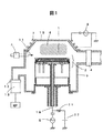
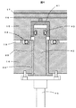
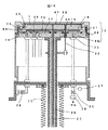
以下、本発明の実施例を図にしたがって説明する。図1、2に本発明の第一の実施例を示す。図1は本発明のウエハステージをプラズマ処理装置に適用した例、図2は図1に示すウエハステージを拡大した図、図3は水冷ジャケットの斜視図である。
【0013】
図1に示すように、真空チャンバ9内にエッチングガス11を導入し、ターボ分子ポンプ13の上流に設置したバルブ12の開度調節によりチャンバ内を適切な圧力に保つ。真空チャンバ9の上部にはアルミナ製のベルジャ10が積載してあり、このベルジャの周囲にはコイル7が設置してある。コイル7を高周波電源8に接続し、コイルの両端に高周波電圧、例えば13.56MHzの高周波電圧を印加することにより誘導結合方式のプラズマ6を発生させる。このプラズマにウエハ1を曝すことによりエッチング処理を実施する。処理中、ウエハはウエハステージ2上に載置され、温度管理されている。
【0014】
また、ウエハにバイアス電圧を印加するために、ウエハステージには高周波電源5を接続している。また、この高周波電源の給電ラインにはウエハステージに静電チャック機能を付与するために直流電源22が接続してある。なお、図において、3はエッチングガスの流量を制御する流量制御器、4はゲートバルブである。ゲートバルブ4はウエハの搬送時には開となり、ウエハを搬送する図示しない搬送アームが前記ゲートバルブ4を通して前進または後退する。
【0015】
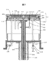
次に、図2、図3を用いて本発明のウエハステージを詳細に説明する。ウエハステージ2は大きく分けると、冷却用の水冷ジャケット14の上に、ヒータ機能及び静電チャック機能を有するセラミックス板15をボルトで固定して搭載した構成となっている。
【0016】
セラミックス板15の材質は熱伝導率の大きな窒化アルミであり、内部にヒータ16を埋設してある。したがって、ヒータ16に電力を投入することによりセラミックス板を加熱することができる。なお、セラミックス板を窒化アルミで構成するのは、窒化アルミは熱伝導率が高いため面内に温度差がつきにくくなり、ウエハの温度分布を均一化することができるためである。しかし、必ずしも窒化アルミである必要があるわけではなくその他の材質であってもよい。
【0017】
また、前記セラミックス板15内部のヒータ16上には、ウエハステージに静電チャック機能及びRFバイアスを与えるための内部電極17を埋設してある。この内部電極17に直流電圧を印加すれば、内部電極17とウエハ1(ウエハはプラズマに曝されておりほぼアース電位)間に電位差が発生し、内部電極とウエハ裏面間に電荷が蓄えられてクーロン力によりウエハはセラミックス板に吸着固定される。また、内部電極17には直流電圧のほかにウエハにバイアス電力を投入するための高周波電圧を印加する。図1の高周波電源5がこの役割を果たす。電気回路的には静電チャック用の直流電源22をコイル21を介して給電ライン19に接続する。本実施例で給電ラインに相当するのは支持部材内に設けた中空のシャフト20である。この中空シャフトを介して内部電極17に高周波電圧を印加してウエハにバイアス電圧を印加すれば、プラズマ中のイオンをウエハに効果的に引き込むことができる。これによりエッチングレートが増加し、更にエッチング形状が改善されるなどの効果が期待できる。
【0018】
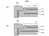
なお、前記ヒータ16及び内部電極17はその配置の仕方によって得られる効果が異なるので以下に説明する。図4(a)には第一の実施例と同様な内部電極17の配置の拡大図を示す。この例の場合では内部電極17はセラミックス板15の凸部内のみに配置してあるため、ウエハのみを吸着し、RFバイアスもウエハのみに印加される。すなわちサセプタ75は静電吸着されず、RFバイアスもかからない。したがって、サセプタ75はプラズマによりエッチングされることがない。これに対して図4(b)の例の場合には、セラミックス板の内部電極17と電気的に接続した第二の内部電極76が内蔵されている。この方式ではウエハだけでなくサセプタ75も静電吸着され、更にサセプタ75にRFバイアスも印加されることになる。すなわち、この方式はデポ性(堆積性)の強いエッチングプロセスに有利な方法を提供する。すなわち、デポ性が強いプロセスの場合、図4(a)の方式ではサセプタにデポ(堆積物)が付着し、次いで、付着した前記堆積物が剥離してウエハ表面に異物として載ることがあり、歩留まりの低下を引き起こす。これに対して図4(b)の例の場合には、サセプタに付着した堆積物はRFバイアスが印加されることによりエッチングされ、結果としてウエハ表面に付着する異物が少なくなり歩留まりが上がるという利点がある。
【0019】
次に、図5を用いてヒータの外径の違いによる効果の違いを説明する。図5(a)は第一の実施例と同じように、ヒータ16の外径をセラミックス板の凸部の外径とほぼ同じに配置した場合である。この場合は、プラズマからの入熱量が大きい場合に、ウエハ温度分布を均一化する手法として有効な方法である。つまり、図5(b)のヒータ外径をセラミックス板の凸部より大きくして、セラミックス板の外径付近まで伸びている場合には、セラミック板のほぼ全面にわたり均一に加熱できるので、プラズマ入熱がないか、もしくは入熱が小さい場合にはウエハ温度分布を均一化しやすいメリットがある。しかし、プラズマ入熱が大きい場合には、セラミックス板の温度を下げる必要があるためにヒータへの出力を小さくする必要がある。この場合は外周付近の入熱量に比べて凸部領域の入熱量が相対的に大きくなってしまう。その結果、ウエハ外周の温度が相対的に低くなりウエハ面内に温度分布が発生してしまう。
【0020】
これに対し、図5(a)の場合にはヒータは凸部領域とほぼ同じ範囲となっており、このヒータ配列でウエハ温度分布が均一化されているため、プラズマ入熱が大きく、ヒータ出力が低下した場合でも、もともとの状態とほぼ同じ領域のみの入熱分布となるので、結果ウエハ温度分布が悪化することがない。
【0021】
なお、前記内部電極の構造やヒータ外径に関しては、実際に使用する場合の条件に応じて適宜、最適化しておけばよい。また、本発明はこれらをいずれの組み合わせで使用するかを限定するものではない。
【0022】
以上のように、内部電極にバイアス電圧を印加してウエハを処理するとウエハはプラズマからの入熱により温度が上昇する。入熱量が小さい場合には問題にならない場合もあるが、通常半導体の製造プロセスではウエハの温度管理をしっかり行わないとエッチング特性が悪化する。前述したようにウエハの温度を高温に保つためには、プラズマからの入熱がないときにはヒータによりセラミックス板を加熱し、処理が始まりプラズマからの入熱があるときにはウエハへ入射した熱を取り除く必要がある。このための対策として、本実施例では、図2に示すようにセラミックス板15と水冷ジャケット14間に0.5mmのギャップ18を設け、このギャップに1kPa以下程度の圧力のヘリウムガスを導入している。23はヘリウムガス導入口、24はヘリウムガス排気口である。つまり、プラズマからの入熱が無くウエハを高温に保持する必要がある場合にはバルブ25を閉じバルブ26を開くことによりギャップ内の圧力を処理室と同一(通常数Pa以下程度)とし、これにより真空断熱する。一方、プラズマからの入熱によりセラミックス板を冷却する必要がある場合にはバルブ25を開きバルブ26を閉じギャップにヘリウムガスを導入しセラミックス板から水冷ジャケットへの熱の流れを確保し冷却する。この際、ギャップ内のヘリウムガスの圧力はバルブの下流に圧力計27を設けておき流量制御器28の動作を制御すればよい。
【0023】
また、ウエハを処理する処理室の圧力は前述したように数Pa以下程度であるため、ウエハ裏面とセラミックス板間にもヘリウムガスなどの伝熱ガスを導入する必要がある。本実施例では、内部電極に高周波電圧と直流電圧を印加する支持部材に内蔵された中空のシャフトを通じて供給される。すなわちセラミックス板の中心に設けた貫通穴からヘリウムガスをウエハ裏面に導入する構成となっている。
【0024】
水冷ジャケットの内部には冷却用に水を循環させるための溝46が設けてある。本実施例では冷却水はクリーンルーム内に装備された冷却水を使用している。溝への冷却水の流し込みと排水はフレキシブルな配管(図示しない)を使用する。また、バルブ25とヘリウムガス導入口23間の配管はフレキシブルな配管30を使用する。これにより、ウエハステージ2全体の上下動に対応することができる。また、図中には冷却水の入り口のみを記載し、戻り側は省略している。なお、本実施例では、冷媒として水を利用したが必ずしも水に限るものではない。例えばフロリナートやガルデン(いずれも商品名)といたフッ素系の冷媒を使うことも可能である。しかし、水を使用する場合は、冷媒を循環させる部品(本例では水冷ジャケット)との間の熱伝達率が大きいために、ギャップ18のヘリウムガス圧力が同一の場合、セラミックス板との間の熱移動量が大きく取れるメリットがある。逆にいえば、同じ熱移動量を確保するために必要な圧力が低くてすむ。すなわち、装置設計を行う上で、ヘリウムのシール条件が緩和されるので大きなメリットとなる。
【0025】
ウエハの搬送は、図示しない上下機構によるベローズ35の伸縮動作によりウエハステージ2を上下動作させ、固定しているプッシャピン32によりウエハをセラミック板から引き剥がすことにより行うことができる。
【0026】
次に、本発明の特徴である、500℃程度の高温までの広い温度範囲にわたり応答性よく、かつ均一な分布でウエハ温度を制御するためになされた対策について説明する。
【0027】
本実施例のように、セラミックス板と水冷ジャケット間にヘリウムガスを導入する場合には、ヘリウムガスのリークを抑えることが重要な技術課題となる。本実施例では、ウエハステージを500℃程度の高温領域まで使用できるように、従来技術のようなOリングを使用せず、内部にコイルバネを保持した金属性のシールを使用する。例えば、図2及び図3において、31及び31’は水冷ジャケット14の外周から処理室にリークするのを防止するためのシール及びシール嵌入溝である。また、ウエハをステージから引き剥がし搬送するためのプッシャピン32の周りには径の小さな同様の機能を有するシール33及びシール嵌入溝を使用している。また、ヒータへの給電部34まわりや、セラミックス板の温度を測定するためのシース熱電対(図1、2には記載せず。後に説明。)のまわりにもそれぞれの部品のサイズに合った適切な径のシール及びシール嵌入溝が設けてあり、ヘリウムガスのリークを防止している。本実施例のシールを使用した場合、Oリングとは異なり500℃程度の高温まで十分利用できる。また、単なるメタルシールの場合と比べても、内部のコイルバネの弾性作用により締め付けトルクが小さくてすむ、熱膨張によりシールする部材の位置関係が多少変化しても追随してシール効果が持続する、あるいは繰り返し使用可能である、などの効果が期待できる。また、本実施例ではメタルシール内に設けたバネはコイルバネであったが、その他に板バネなども考えられる。重要なのはシールが内部に保持した弾性を有する部材で変形可能であるという点である。
【0028】
次の対策として、本実施例ではウエハ温度分布を均一化するために、セラミックス板の温度分布を均一化する。このため、セラミックス板を水冷ジャケットに固定するためのボルトを通しての伝熱、及びセラミックス板から水冷ジャケットへの熱の逃げあるいは水冷ジャケット側面からの輻射による熱の逃げを低減する対策がなされている。
【0029】
例えば、本発明ではセラミックス板を水冷ジャケット14に固定するボルトを介して伝導するの局所的な熱の逃げを低減するためにジルコニアセラミックス製ボルト36を使用している。ジルコニアセラミックスは熱伝導率が3W/mK程度と非常に熱伝導率が低い上、破壊靭性値も大きく機械強度的に優れた特徴を持っている。したがって、セラミックス板を固定するボルトの材料として適している。
【0030】
また、本実施例ではセラミックスの板が500℃程度の高温まで加熱された場合にも、セラミックスネジが折れることが無いよう、セラミックス板に設けたボルト穴の径がセラミックス板の熱膨張を許容する程度に大きする工夫がなされている。具体例で説明する。本実施例ではジルコニアボルトはM4ネジであり、半径110mmの位置で固定するように設計されている。セラミック板が室温の20℃から500℃に加熱された場合、熱による半径方向の膨張はジルコニアの膨張係数が5×10⁻⁶(1/K)であることから、(500−20)×5×10-6×110=0.26mmとなる。したがって、最低でも片側0.26mmは余裕を見る必要があり、この場合4.52mmとなる。しかし実際には組み立ての余裕を見てφ5としている。
【0031】
次に、本実施例ではセラミックス板からの輻射による熱の逃げを防止する目的で、水冷ジャケットの表面37には鏡面研磨が施されている。水冷ジャケットの表面を鏡面研磨した場合とそうでない場合の熱の逃げを見積もってみる。本実施例ではセラミックス板の直径は240mmであった。セラミックス板の表面の放射率は0.8で、水冷ジャケットの表面の放射率は鏡面研磨しない状態では0.3、鏡面研磨した状態では0.1であった。放射率の測定は試料を加熱して放射率を測定する直接法や、FTIRを用いて反射スペクトルを測定し得られた分光反射率をもとに算出する間接法で測定可能である。水冷ジャケットは冷却され30℃に保たれており、セラミックス板の温度を500℃に保った場合、研磨しなかった場合には約250Wもの熱量が逃げることになる。これに対し、鏡面研磨した場合では約90Wとおよそ1/3程度まで低減される。
【0032】
次に、セラミックス板の外周からの熱の逃げを低減するために、本実施例ではセラミックス板を囲むように表面にクロムめっきを施した輻射断熱材38を設けている。前記輻射断熱材の効果について見積もってみる。本実施例ではセラミックス板の厚みは20mmであった。輻射断熱材が無い場合、室温程度(仮に25℃とする)に保たれた真空チャンバの内壁(放射率0.3と仮定する)へにげる輻射熱は約80Wであるが、輻射断熱材ありの場合(表面の放射率を0.1と仮定する)約30Wと半分以下に抑えられる。
【0033】
なお、本実施例では水冷ジャケットの上面は鏡面研磨、輻射断熱材の表面にはクロムめっきした構造としているが、必ずしもこのような組み合わせである必要は無い。両方ともクロムめっきであってもよいし、鏡面研磨であってもよい。また、セラミックス板の表面には特に加工を施していないが、こちらの面にも表面の放射率を下げるような材料をコーティングすることも可能である。また、本実施例ではめっきとしてクロムめっきを適用しているが必ずしもこれに限るわけではなく、そのほかの材料例えばニッケルや銅などであってもよい。また、本実施例では輻射断熱材はセラミック板の外周に1個となっているが、必ずしも1個である必要は無く複数個重ねた構造とすれば断熱効果がさらに高まり、セラミック板の外周付近の温度分布がさらに均一化する効果を期待することができる。
【0034】
次に、図6,7,8を用いて本発明の第一の実施例のヒータ16および内部電極17への給電部の構造を説明する。まず図6を用いてヒータへの給電部について説明する。水冷ジャケット14に貫通穴39を設け、この貫通穴に嵌合するように絶縁用セラミックパイプ40を挿入する。セラミック板15には水冷ジャケットの貫通穴に対応する位置に電気プラグ41が埋め込まれており、内部のヒータ16と導通している。この電気プラグに挿入する形で端子42がセラミックパイプを貫通して取りつけられる。端子及びシャフトの先端付近には、端子と電気プラグのコンタクトを確実にするため、図8に示すような螺旋状の導電体を円形に曲げて形成したバネ部材43を嵌合してある。44はギャップ18内のヘリウムガスがリークしないようにするためのシールである。45は配線であり、外部のヒータ電源に接続している。本実施例ではヒータ給電部は1ヶ所のみの記載としているが、実際には反対の極性のコネクタが必要であるので、給電部は2ヶ所となる。
【0035】
次に、内部電極17への給電部の構造を図7を用いて説明する。水冷ジャケットの中心に貫通穴を設け、この中に絶縁用のセラミックパイプ48を埋め込んでいる。このセラミックパイプの中にはシャフト20と、電気絶縁用のポリテトラフルオロエチレン製の絶縁パイプ47を挿入する。シャフトの先端付近にはヒータへの給電部と同様に電気コンタクトを確実にするためのバネ部材43が設けてある。セラミックス板15に埋め込まれた電気プラグ51にボルト49で固定したガイド50はバネ部材43を介してシャフト20と接続している。電気プラグ51は内部電極17と電気的に接続してあり、以上の経路により内部電極に静電チャック用の直流電圧と高周波バイアス電圧を印加することができる。52はヘリウムを封止するシールである。
【0036】
このように、セラミックス板内に形成した内部電極及びヒータに給電する部分の接続構造をセラミックス板の下側からバネ部材を介して接続する構造としているのでセラミック板の着脱を容易に行うことができる。また、ばねの弾性変形を利用しているので電気接触が確実になり、接触不良を起こすことことがない。また、バネの弾性変形により電気接触が確実となるので、セラミックス板が高温になって熱膨張し、プラグ側との隙間が変化した場合にも接触が持続できるという効果も期待できる。したがって、広い温度範囲にわたり電気接続を実現可能となる。
【0037】
次に、ヒータの出力、ヘリウムガス圧を決定するために必要なセラミックス板の温度測定方法を図9により説明する。水冷ジャケット14の一部に貫通穴54を設け、この貫通穴に対応するセラミックス板15の裏面にくぼみ53を設ける。くぼみの直径は、シース熱電対の直径にセラミックス板の最高使用温度における熱膨張を許容できる余裕を見た程度とするのが望ましい。例えばシース熱電対の直径が3mm、温度が500℃、取りつけ位置が半径80mmの位置の場合、室温20℃からの膨張は、ジルコニアの膨張係数が5×10⁻⁶(1/K)であることから、(500−20)×5×10-6×80=0.19mmとなる。したがって、最低でも片側0.19mmは余裕を見る必要があり、この場合3.38mmとなる。しかし実際には組み立ての余裕を見て4mmとしている。このくぼみの底面に先端が接触するようにシース熱電対55を挿入する。先端の接触状態が変化すると測定する温度が変化してしまうので、本実施例では熱伝対に鍔56をもうけ、この鍔の部分にコイルバネ57を嵌合し、更に支持部材59に固定したおさえ58によりシース熱電対全体をセラミックス板15方向に押圧している。
【0038】
したがって、セラミックス板の取り付けの状態が多少変化してもシース熱電対の先端とセラミックス板の接触圧力は常にほぼ一定となり再現性のよい温度測定方法を提供することができる。
【0039】
このほかのセラミックス板の温度測定法としては、放射温度計を利用することが考えられる。この場合、放射温度計の先端はセラミックス板と非接触でよいので、接触の状態を一定に保つといった機構は不要となる利点がある。
【0040】
以上の温度測定法では直接ウエハの温度を測定することはできない。しかしながら、あらかじめセラミックス板とウエハ温度の相関関係を実験により明らかにしておけば、ウエハ温度を予想することは可能である。また、ウエハには直接温度測定用のプローブを接触させることが無いので裏面異物を増加させるといった心配が無い。
【0041】
以上説明したように、本実施例の構成によれば、セラミックス板を加熱する場合には、セラミック板と水冷ジャケットとのギャップ内を真空引きして断熱し、ヒータに電力を投入することで高速にセラミックス板を加熱することができる。また、ウエハ処理時にプラズマから入熱がある場合にはセラミックス板と水冷ジャケットに間にヘリウムガスを流すことにより前記入熱を取り除くことができ、これによりウエハ温度を一定に保つことができる。またシールにはOリングを使用せず内部にコイルバネを保持した金属性のシールを使用しているので、500℃程度の高温まで幅広い温度範囲でウエハを処理することが可能となる。また、セラミックス板は水冷ジャケットに溶接されているわけではないので、交換が必要な場合にはセラミックス板のみを容易に交換することができる。
【0042】
なお、本実施例では、シールとしてコイルバネを内蔵した金属製のシールを使用したが、必ずしもこれに限る必要はなく、例えば耐熱温度の高い高分子材料のシールなどを使用してもよい。この場合、金属性のシールに比べ剛性が低いのでセラミックス板を固定するためのボルトの締め付けトルクが小さくてすむという効果が期待できる。
【0043】
また、セラミックス板を固定するボルトをジルコニアセラミックスとしているので、ボルトを介してにげる熱量が小さくてすみ、ヒータに投入する電力が小さくランニングコストを下げることができる。また、セラミックス板の外周付近からの熱の逃げが少なくてすむので外周付近の温度低下を抑える事ができ、結果としてウエハ温度分布の均一性を損なうことが無い。
【0044】
また、セラミックス板の周りを輻射断熱効果の高い構造としているのでセラミックス板に投入するヒータ電力を低減することができるためランニングコストを抑える効果が期待できる。また、セラミックス板の外周からの輻射による熱の逃げが抑えられるので、セラミックス板外周付近の温度低下を防止することができ、結果としてウエハ面内温度分布を均一にすることができる。
【0045】
次に、実際の生産現場で本発明の処理装置を使用する場合において作業者が設定すべき設定項目、特にウエハの温度を設定するための設定項目(例えばRFバイアス電力、ヒータ出力、ウエハ裏面のヘリウム圧力、ギャップのヘリウム圧力)について説明する。
【0046】
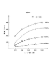
図10は、本実施例の処理装置でRFバイアスを500W、ウエハ裏面のヘリウムガス圧力を1kPaとし、ギャップ18のヘリウム圧力をパラメータとした場合のヒータ出力とウエハ温度の関係を表すグラフである。このグラフはあらかじめ実験、もしくは計算により算出することができる。このようなグラフを各バイアス電力ごとに用意しておく。従って、作業者はこのグラフを用いればこれから処理する条件でのウエハ温度を容易に予測することができる。また、逆に必要なウエハ温度がどのヒータ出力、ギャップのヘリウム圧力で実現できるか読み取ることができるので、作業効率を改善することができる。
【0047】
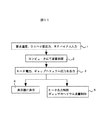
図11は、この手順を自動化した例を示している。この例では、まず作業者が希望の処理温度、ウエハ裏面のヘリウム圧力、RFバイアス電力を設定する(ステップ1)。この情報はコンピュータへおくられ、内部に用意された図10に示す情報を元に演算処理し(ステップ2)、必要なヒータ出力、ギャップのヘリウム圧力を計算する。結果は、最終的に作業者が手動で設定する場合には、表示器に出力する(ステップ4)。また、計算結果を元に自動で処理する場合にはヒータの制御装置及びギャップへヘリウムを流す流量制御器28を制御する(ステップ5)。
【0048】
これらの方法の利点は、はじめに作業者が新しいプロセスを実施する場合に条件を容易に設定しやすいという点にある。なお、前記ウエハの温度を設定する設定項目としては、前述の例の他に冷媒の温度、流量も考えられるが、冷媒として水を数リットル毎分流す程度の場合には、あまり問題になることが無いのでここでは省略した。しかし、温度に影響するような領域での使用条件であるならば、あらかじ設定項目として考慮しておくことはウエハ温度制御の観点から重要である。
【0049】
以上説明したように本発明の第一の実施例によれば、広い温度範囲においてウエハの温度を均一に、少ない電力で処理可能である。また、本実施例を拡張することで処理中の温度分布をアクティブに変更することが可能となる。以下にそれを説明する。
【0050】
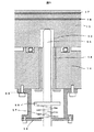
図12は、本発明の第二の実施例である。本実施例ではセラミックス板60の内部に設けたヒータを外周ヒータ61と内周ヒータ62で独立させた構造となっている。また、図示しないがウエハ内周付近の温度と外周付近の温度をそれぞれ測定すべくシース熱電対を半径方向に2箇所設けている。これら2個の温度計で測定された温度情報にもとづき各ヒータに投入する電力を制御することができる。なお、図8では簡略化のためにプッシャピン機構は省略している。
【0051】
このような構成であれば、ウエハ面内に温度分布を発生させたい場合、各ヒータの投入電力を変更することにより容易に実現可能となる。これにより所望のエッチング特性を得ることが可能となる。
【0052】
本実施例ではヒータは中心付近と外周付近の2つの領域に分割されていたが、必ずしも2分割である必要は無く、異なるパターンであってもよいし、3分割でもよい。必要なウエハ温度分布を実現するように適宜決定されるべきものである。
【0053】
図13には本発明の第3の実施例を示す。本実施例では水冷ジャケット63とセラミックス板15間に設けたギャップ内に内周と外周を分割するように凸部64を設け、内周と外周に独立にヘリウムを導入、排出する機構を設けている。図中には内側導入口65と外側導入口66のみを記載し、ヘリウムの排出口は記載していない。また、簡略化のために、プッシャピン機構及びヒータ給電部は省略している。このような構成において、内側領域及び外側領域のヘリウムガス圧力を変化させればセラミックス板との熱コンダクタンスを変化させることができるため、結果的にウエハ温度分布を制御することが可能となる。本実施例では、分割する凸部には特にシールを設けていないが、コンダクタンスが十分小さいので内側と外側に圧力差をつけることができる。しかし、必要なら凸部にシール部材を設ければより厳密に内側と外側の圧力を制御することが可能となる。
【0054】
以上の各実施例ではウエハ裏面とセラミックス板間に導入するヘリウムはすべて中心から導入していた。しかし、必ずしもそうである必要は無く、ウエハ外周付近に導入してもよいし、中心と外周の両方から導入してもよい。装置設計のしやすさ、望ましいウエハ温度分布などの観点から適宜決定されればよい。
【0055】
また、本発明の第二、第三の実施例を組み合わせて実施すれば、処理中のウエハの温度、もしくはロット内のウエハの温度、もしくはロット間のウエハの温度をさらに効果的に制御することが可能となる。
【0056】
また、以上の各実施例ではウエハを固定するための静電チャックは内部電極が単極のいわゆるモノポール方式と呼ばれるものであったが、必ずしもこれだけに限定されるべきものではない。すなわち、静電チャック用の内部電極として独立した2個の電極を有するいわゆる双極方式と呼ばれる方式であってもよい。この方式では、内部に2個の電極を必要とするので構造が複雑となる、あるいは電源が2個必要となるなどの欠点はある。しかし、プラズマが発生していなくともウエハを吸着することができるため、すなわちプラズマ処理を開始する前からウエハ裏面に冷却ガスを導入することができるため温度制御性に優れるという利点がある。
【0057】
また、以上の各実施例の処理装置のプラズマ源は誘導結合方式のプラズマであることを前提としたが、必ずしもこの方式に限定されるべきものではない。例えば、平行平板方式のプラズマ源であってもよいし、UHF帯電磁波放射放電方式やマイクロ波方式、あるいは数10MHzから300MHz程度までのVHF帯を用いたプラズマ方式でもよい。これ以外にも、たとえば磁場を用いたマグネトロン型のプラズマ処理装置などであってもよい。これの方式の内、いずれのプラズマ現を採用するかは、実際に処理すべき材料の特性にあったものを採用すべきものであり、適宜選択すればよい。
【0058】
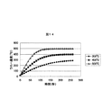
次に本発明の第四の実施例を図14、15を用いて説明する。半導体ウエハを500℃のような高温で処理する場合、半導体ウエハを急激に加熱すると熱衝撃により割れる場合がある。そこで本実施例では、半導体ウエハを処理室内のウエハステージ上に搬送後、所定時間保持して予熱するプロセスを導入する。図14にウエハステージの温度(300℃、400℃、500℃)毎に半導体ウエハの温度上昇特性を示す。この図から、ウエハステージの温度毎の時定数(t秒)がわかる。
【0059】
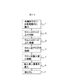
図15は、ウエハの搬送処理を示すフローチャートである。図に示すようにウエハの搬送処理は、半導体ウエハを処理室内に搬入し(ステップ1)、搬入したウエハをウエハステージ上で保持した状態で、処理プロセス毎に異なる所定時間(例えば前記時定数時間)予熱する(ステップ2)、予熱が終了したらウエハをウエハステージ上に載置する(ステップ3)。次いでウエハにプラズマ処理を施し(ステップ4)、処理が終了したらウエハを搬送室に搬送する(ステップ5)。次いで搬送室に窒素ガスを導入してウエハを冷却し(ステップ6)、所定温度まで冷却したらウエハを取り出す。
【0060】
このように本実施例では、所定時間の予熱時間を設けている。このプロセスは1枚あたりのウエハの処理時間を増加させるが、ウエハの熱衝撃による割れを防ぐことができる。このため、本実施例の処理方法では結局は装置の稼働率改善の効果を期待することができる。
【0061】
一方、ウエハを搬出する場合には、半導体ウエハを処理室からバッファ室(搬送室)に移動後、ウエハ温度を下げるプロセスが必要である。そこで本実施例では、バッファ室に移動後、ウエハを取り出さない状態で窒素ガスを導入し、バッファ室のチャンバに熱を移動させてウエハを冷却する。この方法を使えば簡便にウエハを冷却することができ、作業者が誤って触れた場合などにも安全である。
【0062】
以上の実施例では、セラミックス板内に内部電極とヒータを内蔵した構造としたが、その他の高温エッチング対応のウエハステージについて説明する。
【0063】
図16には本発明の第五の実施例を示す。本実施例では、内部にヒータ配線70を内蔵したセラミックヒータ69と、アルミ基材67の表面にセラミックスの溶射膜68を設けた構造体をロウ付けして一体化し、この構造体をジルコニアボルト36を用いて水冷ジャケット14に固定している。この例では溶射膜68が静電チャック用の誘電体膜として機能する。アルミ基材への給電はシャフト20により行われており、アルミ基材とシャフトの電気接触部には第一の実施例同様にコイルバネ状のバネ部材を使用しており広い温度範囲での使用を可能にしている。したがってシャフトを介して第一の実施例と同様に直流電圧とRFバイアス電圧を印可すれば、ウエハを吸着固定しRFバイアスを印加することができる。セラミックスヒータと水冷ジャケットとの熱のやり取りは、第一の実施例と同様、ギャップ18にヘリウムガスを導入しており、処理室へのリークを抑えるシールは第一の実施例同様に内部に弾性を有する構造体を内蔵した金属製のシールである。また、アルミ基材とセラミックスヒータの外周には輻射による熱の逃げを防止する輻射断熱材38を設けている。この様な構成とすれば、第一の実施例と同様な効果を期待できるほか、静電チャック用の誘電膜を製造コストの低い溶射法により製作できる点があげられる。
【0064】
図17には本発明の第六の実施例を示す。本実施例では、アルミ基材67とセラミックスヒータ69を、アルミ板71を挟んでジルコニアセラミックボルト36で固定している。アルミ板71の作用はアルミ基材67とセラミックヒータ69の熱接触を改善することである。したがって、必ずしもアルミである必要は無く、その他の金属、熱伝導グリースなど、熱伝導を改善するものであれば何であってもよい。セラミックヒータ69は水冷ジャケット14に対して、セラミックスボルト73で固定されている。その他の構成は第五の実施例と同様、第一の実施例の技術が適用されている。したがって、この様な構成であれば第一の実施例と同様の効果を期待できるほか、静電チャック用の誘電膜を製造コストの低い溶射法により製作できるだけでなく、アルミ基材のみを容易に着脱可能であるため、静電チャックの交換にアルミ基材のみの交換ですみ、コストが安い、メンテナンス性がよいといった効果を期待できる。
【0065】
以上説明したように本発明の各実施例によれば、低温から高温までの広い範囲にわたりウエハを均一な温度分布で、処理中も温度変動を少なく保持することができる。したがって、通常のプロセスではエッチンすることができないような不揮発性材料もエッチング処理することができるようになる。
【0066】
また、低温から高温までの広い温度範囲で処理中のウエハ温度分布をアクティブに制御することが可能となる。ウエハを高温に加熱する場合において熱衝撃により割れることのない処理方法を提供することができる。更にウエハを搬出する場合にも作業者が高温のウエハに触れた場合においても安全な処理方法を提供することができる。
【0067】
【発明の効果】
以上説明したように本発明によれば、広い温度範囲でウエハの温度分布を均一に保つことができるウエハステージを提供する。また、ウエハに温度変化による障害を与えることのないウエハ処理方法を提供することができる。
【図面の簡単な説明】
【図1】本発明の第1の実施例を示す図である。
【図2】図1に示すウエハステージの拡大図である。
【図3】水冷ジャケットの斜視図である。
【図4】内部電極の拡大図である。
【図5】内部電極の拡大図である。
【図6】ヒータへの給電部の構造を説明する図である。
【図7】内部電極への給電部の構造を説明する図である。
【図8】端子あるいはシャフトとその先端付近に嵌合するバネ部材を説明する図である。
【図9】セラミックス板の温度測定方法を説明する図である。
【図10】ヒータ出力とウエハ温度の関係を示す図である。
【図11】ウエハの処理条件を自動的に予測する手順を説明するである。
【図12】本発明の第2の実施例を示す図である。
【図13】本発明の第3の実施例を示す図である。
【図14】本発明の第4の実施例を示す図である。
【図15】本発明の第4の実施例を示す図である。
【図16】本発明の第5の実施例を示す図である。
【図17】本発明の第6の実施例を示す図である。
【符号の説明】
1…ウエハ、2…ウエハステージ、3…流量制御器、4…ゲートバルブ、5…高周波電源、6…プラズマ、7…コイル、8…高周波電源、9…真空チャンバ、10…ベルジャ、11…エッチングガス、12…バルブ、13…ターボ分子ポンプ、14…水冷ジャケット、15…セラミックス板、16…ヒータ、17…内部電極、18…ギャップ、19…給電ライン、20…シャフト、21…コイル、22…直流電源、23…ヘリウム導入口、24…ヘリウム排気口、25…バルブ、26…バルブ、27…圧力計、28…流量制御器、29…貫通穴、30…フレキシブルな水配管、31…シール、32…プッシャピン、33…シール、34…ヒータ給電部、35…ベローズ、36…ジルコニアセラミックス製ボルト、37…水冷ジャケット表面、38…輻射断熱材、39…貫通穴、40…絶縁用セラミックスパイプ、41…電気プラグ、42…端子、43…バネ部材、44…シール、45…配線、46…溝、47…絶縁パイプ、48…セラミックスパイプ、49…ボルト、50…ガイド、51…電気プラグ、52…シール、53…くぼみ、54…貫通穴、55…シース熱電対、56…鍔、57…コイルバネ、58…おさえ、59…支持部材、60…セラミックス板、61…外周ヒータ、62…内周ヒータ、63…水冷ジャケット、64…凸部、65…内側導入口、66…外側導入口、67…アルミ基材、68…溶射膜、69…セラミックスヒータ、70…ヒータ配線、71…アルミ板、72…ボルト、73…セラミックスボルト、74…伝熱体、75…サセプタ、76…第二の内部電極[0001]
BACKGROUND OF THE INVENTION
The present invention relates to a wafer stage for a wafer processing apparatus, and more particularly to a wafer stage suitable for high temperature (about 200 to 500 ° C.) processing.
[0002]
[Prior art]
As a capacitor electrode material for next-generation semiconductor devices, ruthenium, its oxide, platinum or the like is a promising candidate because of its compatibility with a capacitor dielectric film having a high dielectric constant. In addition, zirconium oxide, hafnium oxide, etc. are considered as gate insulating films instead of silicon oxide, and PZT (compound of platinum, zirconium, and titanium), BST (compound of barium, strontium, and titanium) are examined as capacitor insulating films. ing. As described above, various new materials are being studied as future semiconductor device materials. However, these new materials are thermally and chemically stable and have very low volatility and are called non-volatile materials.
[0003]
In the etching process of these nonvolatile materials, it is essential to keep the temperature of the wafer being processed at a high temperature. In the conventional etching processing apparatus, the temperature of the wafer is generally from a low temperature of about −50 ° C. to about 100 ° C. However, at this temperature, the nonvolatile material cannot be etched because it is chemically stable. For this reason, when using the said non-volatile material, it is necessary to process at high temperature of 200 to 500 degreeC.
[0004]
In order to realize a processing apparatus for processing a wafer at a high temperature, a wafer stage that can not only heat the wafer to a high temperature but also can control the temperature of the wafer uniformly and responsively even when there is heat input from plasma. Necessary.
[0005]
In JP-A-7-176601, a gas gap space is provided between a pedestal holding a wafer, a heat source and a sink provided thereunder, and the pressure of the gas introduced into the gas gap space is controlled. A method for controlling the temperature of the wafer with high responsiveness is shown.
[0006]
Japanese Patent Laid-Open No. 2001-11085 provides a heat transfer gas chamber in which gas can be enclosed and discharged between a holding member for holding a wafer and a cooling member for cooling, and a heating element on the holding member side. To keep the wafer at a high temperature.
[0007]
[Problems to be solved by the invention]
In the example of JP-A-7-176601, the pedestal and the heat sink are welded or the O-ring is sandwiched in order to seal the gas in the gap space provided between the pedestal holding the wafer and the heat sink. Are fixed. In the case where the pedestal and the heat sink are fixed by welding, when the pedestal holding the wafer is replaced due to a lifetime or an accident, the range of replacement tends to be widened and the work becomes large. Also, the connection by welding is limited to metal for both the pedestal and the heat sink. When the O-ring is sandwiched and fixed, the usable temperature range is limited by the heat-resistant temperature of the O-ring, and the upper limit is about 200 ° C. at most.
[0008]
As in the example of Japanese Patent Laid-Open No. 71-176085, the example of Japanese Patent Laid-Open No. 2001-11085 also discloses a method of welding a holding member for holding a wafer and a cooling member, or bolting via an O-ring. Have the same problems as mentioned above.
[0009]
Also, in this example, for the purpose of improving the in-plane uniformity of the wafer temperature, a region with a changed height is provided in the region of the recess provided in the cooling member, and the thermal conductance between the cooling member and the support member is distributed. A method for improving the temperature distribution in the wafer surface is shown. However, in such a configuration, when a cooling member structure capable of realizing an optimized temperature distribution at a certain use temperature is employed, the temperature distribution in the wafer surface may change at other use temperatures. . This phenomenon becomes a problem particularly when used at a high temperature of 400 ° C. or 500 ° C. That is, in the temperature range of 400 ° C. or 500 ° C., heat escape due to radiation from the wafer stage is relatively increased, which causes deterioration of the temperature distribution in the wafer surface. Essentially, it is desirable that the temperature distribution of the wafer stage is uniform over a wide temperature range. For this purpose, there is little heat escape from the wafer stage, and it is advantageous that the heat exchange with the cooling member is uniform in the plane. However, this example does not mention a method for reducing heat escape from the wafer stage. The present invention has been made in view of these problems, and provides a wafer stage that can maintain a uniform temperature distribution of the wafer at a high temperature and in a wide temperature range. In addition, a wafer processing method is provided that does not impair the wafer due to temperature changes during wafer processing using the wafer stage.
[0010]
[Means for Solving the Problems]
The present invention employs the following means in order to solve the above problems.
[0011]
A liquid cooling jacket disposed in a vacuum chamber and having a passage through which a coolant flows disposed therein, and a heater and an electrode for an electrostatic chuck disposed therein, and made of ceramics mounted on the liquid cooling jacket. And a stage on which the wafer is placed on the upper member, and an exhaust pump for exhausting the inside of the vacuum chamber, and processing of the wafer is performed using plasma formed above the stage. A plasma processing apparatus to be performed, the gap being arranged between the liquid cooling jacket and the upper member and sealed inside, and the pressure in the gap while the wafer is placed on the stage And a valve for variably adjusting between a predetermined pressure from a vacuum state.
[0012]
DETAILED DESCRIPTION OF THE INVENTION
Embodiments of the present invention will be described below with reference to the drawings. 1 and 2 show a first embodiment of the present invention. 1 is an example in which the wafer stage of the present invention is applied to a plasma processing apparatus, FIG. 2 is an enlarged view of the wafer stage shown in FIG. 1, and FIG. 3 is a perspective view of a water cooling jacket.
[0013]
As shown in FIG. 1, an etching gas 11 is introduced into the vacuum chamber 9, and the inside of the chamber is maintained at an appropriate pressure by adjusting the opening of a valve 12 installed upstream of the turbo molecular pump 13. A
[0014]
A high
[0015]
Next, the wafer stage of the present invention will be described in detail with reference to FIGS. The
[0016]
The material of the
[0017]
An
[0018]
The
[0019]
Next, the difference in effect due to the difference in the outer diameter of the heater will be described with reference to FIG. FIG. 5A shows a case where the outer diameter of the
[0020]
On the other hand, in the case of FIG. 5A, the heater is in the same range as the convex region, and the wafer temperature distribution is made uniform by this heater arrangement, so that the plasma heat input is large and the heater output is high. Even when the temperature decreases, the heat input distribution is almost the same as that in the original state, so that the wafer temperature distribution does not deteriorate as a result.
[0021]
The structure of the internal electrode and the outer diameter of the heater may be optimized as appropriate according to the conditions for actual use. Moreover, this invention does not limit which combination these are used.
[0022]
As described above, when a wafer is processed by applying a bias voltage to the internal electrodes, the temperature of the wafer rises due to heat input from the plasma. If the amount of heat input is small, it may not be a problem. However, in the semiconductor manufacturing process, the etching characteristics deteriorate if the wafer temperature is not properly controlled. As described above, in order to maintain the wafer temperature at a high temperature, it is necessary to heat the ceramic plate with a heater when there is no heat input from the plasma, and to remove the heat incident on the wafer when the processing starts and heat input from the plasma occurs. There is. As a countermeasure for this, in this embodiment, a gap 18 of 0.5 mm is provided between the
[0023]
Further, since the pressure in the processing chamber for processing the wafer is about several Pa or less as described above, it is necessary to introduce a heat transfer gas such as helium gas between the back surface of the wafer and the ceramic plate. In this embodiment, the internal electrode is supplied through a hollow shaft built in a support member that applies a high frequency voltage and a direct current voltage. That is, helium gas is introduced into the back surface of the wafer from a through hole provided at the center of the ceramic plate.
[0024]
A groove 46 for circulating water for cooling is provided inside the water cooling jacket. In this embodiment, the cooling water used in the clean room is used as the cooling water. A flexible pipe (not shown) is used for pouring and draining the cooling water into the groove. A
[0025]
The wafer can be transferred by moving the
[0026]
Next, a description will be given of measures taken to control the wafer temperature with a responsive and uniform distribution over a wide temperature range up to a high temperature of about 500 ° C., which is a feature of the present invention.
[0027]
When helium gas is introduced between the ceramic plate and the water cooling jacket as in this embodiment, it is an important technical problem to suppress the leakage of helium gas. In this embodiment, a metal seal holding a coil spring is used without using an O-ring as in the prior art so that the wafer stage can be used up to a high temperature region of about 500 ° C. For example, in FIGS. 2 and 3, 31 and 31 ′ are seals and seal insertion grooves for preventing leakage from the outer periphery of the
[0028]
As a next countermeasure, in this embodiment, the temperature distribution of the ceramic plate is made uniform in order to make the wafer temperature distribution uniform. For this reason, measures are taken to reduce heat transfer through bolts for fixing the ceramic plate to the water-cooling jacket and heat escape from the ceramic plate to the water-cooling jacket or radiation from the side surface of the water-cooling jacket.
[0029]
For example, in the present invention, zirconia
[0030]
In this embodiment, the diameter of the bolt hole provided in the ceramic plate allows thermal expansion of the ceramic plate so that the ceramic screw does not break even when the ceramic plate is heated to a high temperature of about 500 ° C. The device is made to a large extent. A specific example will be described. In this embodiment, the zirconia bolt is an M4 screw and is designed to be fixed at a position having a radius of 110 mm. When the ceramic plate is heated from 20 ° C. at room temperature to 500 ° C., the expansion in the radial direction due to heat is such that the expansion coefficient of zirconia is 5 × 10 5. -6 Since it is (1 / K), (500-20) × 5 × 10 -6 × 110 = 0.26 mm. Therefore, it is necessary to allow a margin of 0.26 mm on one side at the minimum, which is 4.52 mm in this case. However, in actuality, φ5 is set to allow for assembly.
[0031]
Next, in this embodiment, the
[0032]
Next, in order to reduce the escape of heat from the outer periphery of the ceramic plate, in this embodiment, a radiant
[0033]
In this embodiment, the upper surface of the water-cooled jacket is mirror-polished and the surface of the radiation heat insulating material is chrome-plated, but such a combination is not necessarily required. Both may be chromium plating or mirror polishing. The surface of the ceramic plate is not particularly processed, but it is possible to coat this surface with a material that lowers the emissivity of the surface. In this embodiment, chrome plating is applied as plating, but the present invention is not necessarily limited to this, and other materials such as nickel and copper may be used. Further, in this embodiment, there is only one radiation heat insulating material on the outer periphery of the ceramic plate. However, it is not always necessary to have a single heat insulating material. The effect of further uniforming the temperature distribution can be expected.
[0034]
Next, the structure of the power feeding portion to the
[0035]
Next, the structure of the power feeding portion to the
[0036]
As described above, since the connection structure of the internal electrode formed in the ceramic plate and the portion for supplying power to the heater is connected via the spring member from the lower side of the ceramic plate, the ceramic plate can be easily attached and detached. . In addition, since the elastic deformation of the spring is used, electrical contact is ensured and no contact failure occurs. Further, since the electrical contact is ensured by the elastic deformation of the spring, the effect that the contact can be maintained even when the ceramic plate becomes hot and thermally expands and the gap with the plug changes is expected. Therefore, electrical connection can be realized over a wide temperature range.
[0037]
Next, a method for measuring the temperature of the ceramic plate necessary for determining the output of the heater and the helium gas pressure will be described with reference to FIG. A through hole 54 is provided in a part of the
[0038]
Therefore, even if the attachment state of the ceramic plate changes somewhat, the contact pressure between the tip of the sheath thermocouple and the ceramic plate is always substantially constant, and a temperature measurement method with good reproducibility can be provided.
[0039]
As another method for measuring the temperature of the ceramic plate, it is conceivable to use a radiation thermometer. In this case, since the tip of the radiation thermometer may be non-contact with the ceramic plate, there is an advantage that a mechanism for keeping the contact state constant is unnecessary.
[0040]
The above temperature measurement method cannot directly measure the temperature of the wafer. However, if the correlation between the ceramic plate and the wafer temperature is clarified by experiments in advance, the wafer temperature can be predicted. Also, since there is no direct temperature measurement probe in contact with the wafer, there is no worry of increasing backside foreign matter.
[0041]
As described above, according to the configuration of the present embodiment, when the ceramic plate is heated, the gap between the ceramic plate and the water cooling jacket is evacuated to insulate, and power is supplied to the heater. The ceramic plate can be heated. In addition, when there is heat input from the plasma during wafer processing, the heat input can be removed by flowing helium gas between the ceramic plate and the water cooling jacket, so that the wafer temperature can be kept constant. In addition, since the seal is made of a metallic seal that does not use an O-ring and holds a coil spring inside, the wafer can be processed in a wide temperature range up to a high temperature of about 500 ° C. Further, since the ceramic plate is not welded to the water-cooled jacket, only the ceramic plate can be easily replaced when replacement is necessary.
[0042]
In this embodiment, a metal seal incorporating a coil spring is used as the seal. However, the present invention is not necessarily limited to this, and for example, a seal made of a polymer material having a high heat resistant temperature may be used. In this case, since the rigidity is lower than that of the metallic seal, an effect that the tightening torque of the bolt for fixing the ceramic plate can be expected to be small.
[0043]
Further, since the bolt for fixing the ceramic plate is made of zirconia ceramics, the amount of heat generated through the bolt can be reduced, and the electric power supplied to the heater can be reduced, so that the running cost can be reduced. In addition, since less heat escapes from the vicinity of the outer periphery of the ceramic plate, the temperature drop near the outer periphery can be suppressed, and as a result, the uniformity of the wafer temperature distribution is not impaired.
[0044]
In addition, since the structure around the ceramic plate has a high radiation heat insulating effect, the heater power input to the ceramic plate can be reduced, so that an effect of suppressing the running cost can be expected. In addition, since heat escape due to radiation from the outer periphery of the ceramic plate can be suppressed, a temperature drop near the outer periphery of the ceramic plate can be prevented, and as a result, the wafer surface temperature distribution can be made uniform.
[0045]
Next, setting items to be set by the operator when using the processing apparatus of the present invention at an actual production site, particularly setting items for setting the wafer temperature (for example, RF bias power, heater output, wafer back surface setting) Helium pressure, gap helium pressure) will be described.
[0046]
FIG. 10 is a graph showing the relationship between the heater output and the wafer temperature when the RF bias is 500 W, the helium gas pressure on the back surface of the wafer is 1 kPa, and the helium pressure in the gap 18 is a parameter in the processing apparatus of this embodiment. This graph can be calculated in advance by experiment or calculation. Such a graph is prepared for each bias power. Therefore, the operator can easily predict the wafer temperature under the processing condition from now on by using this graph. On the other hand, since it is possible to read which heater output and gap helium pressure can achieve the required wafer temperature, the working efficiency can be improved.
[0047]
FIG. 11 shows an example in which this procedure is automated. In this example, an operator first sets a desired processing temperature, helium pressure on the backside of the wafer, and RF bias power (step 1). This information is sent to a computer, and arithmetic processing is performed based on the information shown in FIG. 10 prepared inside (step 2), and necessary heater output and gap helium pressure are calculated. The result is finally output to the display when the operator manually sets it (step 4). Further, in the case of automatically processing based on the calculation result, the controller for the heater and the
[0048]
The advantage of these methods is that it is easy for the operator to easily set conditions when performing a new process. As the setting items for setting the temperature of the wafer, the temperature and flow rate of the refrigerant can be considered in addition to the above-described example. However, when water is used as the refrigerant for several liters per minute, it becomes a problem. I omitted it here. However, if the usage conditions are in an area that affects the temperature, it is important from the viewpoint of wafer temperature control to consider them as setting items.
[0049]
As described above, according to the first embodiment of the present invention, the wafer temperature can be uniformly processed with a small amount of power in a wide temperature range. Further, by extending the present embodiment, it becomes possible to actively change the temperature distribution during processing. This is explained below.
[0050]
FIG. 12 shows a second embodiment of the present invention. In the present embodiment, the heater provided inside the
[0051]
With such a configuration, when it is desired to generate a temperature distribution in the wafer surface, it can be easily realized by changing the input power of each heater. Thereby, desired etching characteristics can be obtained.
[0052]
In this embodiment, the heater is divided into two regions near the center and near the outer periphery. However, the heater is not necessarily divided into two regions, and may have a different pattern or may be divided into three regions. It should be appropriately determined so as to realize a necessary wafer temperature distribution.
[0053]
FIG. 13 shows a third embodiment of the present invention. In the present embodiment, a convex portion 64 is provided in the gap provided between the water cooling jacket 63 and the
[0054]
In each of the above embodiments, all helium introduced between the wafer back surface and the ceramic plate is introduced from the center. However, this is not necessarily the case, and it may be introduced near the outer periphery of the wafer or may be introduced from both the center and the outer periphery. What is necessary is just to determine suitably from viewpoints, such as ease of apparatus design and desirable wafer temperature distribution.
[0055]
Further, when the second and third embodiments of the present invention are combined, the temperature of the wafer being processed, the temperature of the wafer in the lot, or the temperature of the wafer between lots can be controlled more effectively. Is possible.
[0056]
In each of the embodiments described above, the electrostatic chuck for fixing the wafer is a so-called monopole system in which the internal electrode is a single electrode. However, the electrostatic chuck is not necessarily limited to this. That is, a so-called bipolar system having two independent electrodes as internal electrodes for the electrostatic chuck may be used. This method has disadvantages such as the need for two electrodes inside, which complicates the structure, or requires two power supplies. However, since the wafer can be adsorbed even when plasma is not generated, that is, the cooling gas can be introduced to the back surface of the wafer before the plasma processing is started, there is an advantage that the temperature controllability is excellent.
[0057]
Further, although it has been assumed that the plasma source of the processing apparatus of each of the above embodiments is inductively coupled plasma, it should not necessarily be limited to this method. For example, a parallel plate type plasma source may be used, a UHF band electromagnetic wave radiation discharge system, a microwave system, or a plasma system using a VHF band from several tens of MHz to about 300 MHz may be used. Other than this, for example, a magnetron type plasma processing apparatus using a magnetic field may be used. Of these methods, which plasma method to use is selected according to the characteristics of the material to be actually processed, and may be appropriately selected.
[0058]
Next, a fourth embodiment of the present invention will be described with reference to FIGS. When processing a semiconductor wafer at a high temperature such as 500 ° C., if the semiconductor wafer is heated rapidly, it may break due to thermal shock. Therefore, in this embodiment, a process of introducing a semiconductor wafer onto a wafer stage in a processing chamber and holding it for a predetermined time to preheat is introduced. FIG. 14 shows the temperature rise characteristics of the semiconductor wafer for each wafer stage temperature (300 ° C., 400 ° C., 500 ° C.). This figure shows the time constant (t seconds) for each temperature of the wafer stage.
[0059]
FIG. 15 is a flowchart showing a wafer transfer process. As shown in the figure, in the wafer transfer process, the semiconductor wafer is loaded into the processing chamber (step 1), and the loaded wafer is held on the wafer stage, and a predetermined time (for example, the time constant time) varies depending on the processing process. ) Preheat (Step 2), and when preheating is completed, place the wafer on the wafer stage (Step 3). Next, plasma processing is performed on the wafer (step 4), and when the processing is completed, the wafer is transferred to the transfer chamber (step 5). Next, nitrogen gas is introduced into the transfer chamber to cool the wafer (step 6), and after cooling to a predetermined temperature, the wafer is taken out.
[0060]
Thus, in this embodiment, a preheating time of a predetermined time is provided. This process increases the processing time of one wafer, but can prevent the wafer from cracking due to thermal shock. For this reason, the processing method of this embodiment can be expected to improve the operating rate of the apparatus.
[0061]
On the other hand, when unloading a wafer, a process for lowering the wafer temperature after moving the semiconductor wafer from the processing chamber to the buffer chamber (transfer chamber) is necessary. Therefore, in this embodiment, after moving to the buffer chamber, nitrogen gas is introduced without taking out the wafer, and heat is transferred to the chamber of the buffer chamber to cool the wafer. If this method is used, the wafer can be easily cooled, and it is safe even when an operator touches it by mistake.
[0062]
In the above embodiment, the internal electrode and the heater are built in the ceramic plate. However, other high-temperature etching compatible wafer stages will be described.
[0063]
FIG. 16 shows a fifth embodiment of the present invention. In this embodiment, a
[0064]
FIG. 17 shows a sixth embodiment of the present invention. In this embodiment, the aluminum base 67 and the
[0065]
As described above, according to each embodiment of the present invention, the wafer can be maintained in a uniform temperature distribution over a wide range from a low temperature to a high temperature, and the temperature fluctuation can be kept small even during processing. Therefore, non-volatile materials that cannot be etched by a normal process can be etched.
[0066]
In addition, the wafer temperature distribution during processing can be actively controlled over a wide temperature range from low temperature to high temperature. In the case of heating a wafer to a high temperature, it is possible to provide a processing method that does not break due to thermal shock. Furthermore, a safe processing method can be provided even when the wafer is unloaded and when an operator touches the high-temperature wafer.
[0067]
【The invention's effect】
As described above, according to the present invention, a wafer stage capable of maintaining a uniform temperature distribution of a wafer in a wide temperature range is provided. Further, it is possible to provide a wafer processing method that does not give an obstacle due to temperature change to the wafer.
[Brief description of the drawings]
FIG. 1 is a diagram showing a first embodiment of the present invention.
FIG. 2 is an enlarged view of the wafer stage shown in FIG.
FIG. 3 is a perspective view of a water cooling jacket.
FIG. 4 is an enlarged view of an internal electrode.
FIG. 5 is an enlarged view of an internal electrode.
FIG. 6 is a diagram illustrating a structure of a power feeding unit to a heater.
FIG. 7 is a diagram illustrating a structure of a power feeding unit to an internal electrode.
FIG. 8 is a diagram for explaining a terminal or shaft and a spring member fitted near the tip of the terminal or shaft.
FIG. 9 is a diagram illustrating a method for measuring the temperature of a ceramic plate.
FIG. 10 is a diagram illustrating a relationship between a heater output and a wafer temperature.
FIG. 11 illustrates a procedure for automatically predicting wafer processing conditions.
FIG. 12 is a diagram showing a second embodiment of the present invention.
FIG. 13 is a diagram showing a third embodiment of the present invention.
FIG. 14 is a diagram showing a fourth embodiment of the present invention.
FIG. 15 is a diagram showing a fourth embodiment of the present invention.
FIG. 16 is a diagram showing a fifth embodiment of the present invention.
FIG. 17 is a diagram showing a sixth embodiment of the present invention.
[Explanation of symbols]
DESCRIPTION OF
Claims (5)
前記真空チャンバ内側を排気する排気ポンプとを備え、前記ステージ上方に形成したプラズマを用いて前記ウエハの処理が行われるプラズマ処理装置であって、
前記液冷ジャケットと前記上部部材との間に配置されその内側がシールされるギャップと、前記ウエハが前記ステージ上に載置されている間においてギャップ内の圧力を真空の状態から所定の圧力の間で可変に調節するためのバルブとを備えたプラズマ処理装置。A liquid cooling jacket disposed in a vacuum chamber and having a passage through which a cooling liquid flows disposed therein, a heater and an electrode for an electrostatic chuck disposed therein, and a ceramics mounted on the liquid cooling jacket. An upper member, and a stage on which a wafer is placed on the upper member;
An exhaust pump for exhausting the inside of the vacuum chamber, and a plasma processing apparatus for processing the wafer using plasma formed above the stage,
A gap disposed between the liquid cooling jacket and the upper member and sealed inside thereof, and a pressure in the gap is changed from a vacuum state to a predetermined pressure while the wafer is placed on the stage. And a plasma processing apparatus having a valve for variably adjusting between them.
前記真空チャンバ内面を排気する真空ポンプとを備え、前記ステージ上方に形成したプラズマを用いて前記ウエハの処理が行われるプラズマ処理装置であって、
前記液冷ジャケットと前記上部部材との間に配置されその内側がシールされるギャップ内側の圧力を前記処理の通行に応じて真空の状態から所定の圧力の間で可変に調節するプラズマ処理装置。A liquid cooling jacket disposed in a vacuum chamber and having a passage through which a cooling liquid flows disposed therein, a heater and an electrode for an electrostatic chuck disposed therein, and a ceramics mounted on the liquid cooling jacket. An upper member, and a stage on which a wafer is placed on the upper member;
A plasma processing apparatus comprising a vacuum pump for exhausting the inner surface of the vacuum chamber, wherein the wafer is processed using plasma formed above the stage,
A plasma processing apparatus that variably adjusts the pressure inside the gap, which is disposed between the liquid cooling jacket and the upper member and sealed inside thereof, from a vacuum state to a predetermined pressure according to the passage of the processing.
前記ギャップと連通し熱伝達性のガスが供給される導入口と前記ギャップと前記真空チャンバ内の空間とを連通する連通路を備え、この連通路を開いて前記ギャップが前記真空の状態にされるプラズマ処理装置。The plasma processing apparatus according to claim 1 or 2,
An introduction port that communicates with the gap and is supplied with heat transferable gas, and a communication passage that communicates the gap and the space in the vacuum chamber, and opens the communication passage to bring the gap into the vacuum state. Plasma processing equipment.
前記ギャップ内の圧力は、前記プラズマからの入熱が小さな場合に低減され、プラズマからの入熱が大きな場合には増加されるプラズマ処理装置。A plasma processing apparatus according to any one of claims 1 to 3,
The pressure in the gap is reduced when the heat input from the plasma is small, and is increased when the heat input from the plasma is large.
前記ギャップを構成する冷却ジャケットの上面であって前記上部部材と前記ギャップを介して対抗する上面に鏡面加工あるいはメッキ加工された部分を備えたプラズマ処理装置。The plasma processing apparatus according to any one of claims 1 to 4,
A plasma processing apparatus comprising a mirror-finished or plated portion on the upper surface of the cooling jacket constituting the gap and facing the upper member through the gap.
Priority Applications (1)
| Application Number | Priority Date | Filing Date | Title |
|---|---|---|---|
| JP2002049921A JP3881908B2 (en) | 2002-02-26 | 2002-02-26 | Plasma processing equipment |
Applications Claiming Priority (1)
| Application Number | Priority Date | Filing Date | Title |
|---|---|---|---|
| JP2002049921A JP3881908B2 (en) | 2002-02-26 | 2002-02-26 | Plasma processing equipment |
Publications (2)
| Publication Number | Publication Date |
|---|---|
| JP2003249541A JP2003249541A (en) | 2003-09-05 |
| JP3881908B2 true JP3881908B2 (en) | 2007-02-14 |
Family
ID=28662312
Family Applications (1)
| Application Number | Title | Priority Date | Filing Date |
|---|---|---|---|
| JP2002049921A Expired - Fee Related JP3881908B2 (en) | 2002-02-26 | 2002-02-26 | Plasma processing equipment |
Country Status (1)
| Country | Link |
|---|---|
| JP (1) | JP3881908B2 (en) |
Cited By (2)
| Publication number | Priority date | Publication date | Assignee | Title |
|---|---|---|---|---|
| KR20190141260A (en) * | 2017-05-12 | 2019-12-23 | 램 리써치 코포레이션 | Temperature-Tuned Substrate Supports for Substrate Processing Systems |
| KR20220007269A (en) * | 2020-07-10 | 2022-01-18 | 세메스 주식회사 | Apparatus for treating substrate and unit for supporting substrate |
Families Citing this family (46)
| Publication number | Priority date | Publication date | Assignee | Title |
|---|---|---|---|---|
| JP4421874B2 (en) * | 2003-10-31 | 2010-02-24 | 東京エレクトロン株式会社 | Plasma processing apparatus and plasma processing method |
| KR100505035B1 (en) * | 2003-11-17 | 2005-07-29 | 삼성전자주식회사 | Electrostatic chuck for supporting a substrate |
| JP4555647B2 (en) * | 2004-09-21 | 2010-10-06 | 株式会社日立国際電気 | Substrate processing apparatus, semiconductor device manufacturing method, temperature control method |
| US7713432B2 (en) * | 2004-10-04 | 2010-05-11 | David Johnson | Method and apparatus to improve plasma etch uniformity |
| JP4783213B2 (en) * | 2005-06-09 | 2011-09-28 | 日本碍子株式会社 | Electrostatic chuck |
| KR100713334B1 (en) | 2006-05-15 | 2007-05-04 | 동부일렉트로닉스 주식회사 | Temperature control device and control method of etching equipment |
| JP5183058B2 (en) * | 2006-07-20 | 2013-04-17 | アプライド マテリアルズ インコーポレイテッド | Substrate processing with rapid temperature gradient control |
| US9275887B2 (en) | 2006-07-20 | 2016-03-01 | Applied Materials, Inc. | Substrate processing with rapid temperature gradient control |
| JP5042661B2 (en) * | 2007-02-15 | 2012-10-03 | 東京エレクトロン株式会社 | Plasma processing apparatus and filter unit |
| JP2008244224A (en) * | 2007-03-28 | 2008-10-09 | Sumitomo Precision Prod Co Ltd | Plasma processing equipment |
| TW200919578A (en) * | 2007-06-22 | 2009-05-01 | Ulvac Inc | Etching method and etching apparatus |
| JP2009170509A (en) * | 2008-01-11 | 2009-07-30 | Hitachi High-Technologies Corp | Plasma processing apparatus with electrostatic chuck with built-in heater |
| JP2011084770A (en) * | 2009-10-15 | 2011-04-28 | Canon Anelva Corp | Method for controlling substrate temperature by using substrate holder provided with electrostatic chuck |
| US20100014208A1 (en) * | 2008-07-10 | 2010-01-21 | Canon Anleva Corporation | Substrate holder |
| KR101582785B1 (en) * | 2008-08-12 | 2016-01-07 | 어플라이드 머티어리얼스, 인코포레이티드 | Electrostatic chuck assembly |
| JP4879957B2 (en) * | 2008-12-03 | 2012-02-22 | アドヴァンスド・ディスプレイ・プロセス・エンジニアリング・コーポレーション・リミテッド | Substrate processing apparatus having sensing unit |
| JP5230462B2 (en) * | 2009-01-26 | 2013-07-10 | 三菱重工業株式会社 | Substrate support for plasma processing equipment |
| JP2010182729A (en) * | 2009-02-03 | 2010-08-19 | Fuji Electric Holdings Co Ltd | Plasma cvd device |
| WO2010090948A1 (en) * | 2009-02-04 | 2010-08-12 | Mattson Technology, Inc. | Electrostatic chuck system and process for radially tuning the temperature profile across the surface of a substrate |
| CN102067303B (en) * | 2009-02-18 | 2012-11-28 | 株式会社爱发科 | Tray for transferring wafer and method for fixing wafer on the same |
| JP5262878B2 (en) * | 2009-03-17 | 2013-08-14 | 東京エレクトロン株式会社 | Mounting table structure and plasma deposition apparatus |
| JP5375643B2 (en) * | 2009-07-07 | 2013-12-25 | 日新イオン機器株式会社 | Wafer holding mechanism, wafer holder and electrostatic chuck |
| JP5394186B2 (en) * | 2009-10-09 | 2014-01-22 | 日本特殊陶業株式会社 | Parts for semiconductor manufacturing equipment |
| JP5618638B2 (en) * | 2010-06-07 | 2014-11-05 | 株式会社日立ハイテクノロジーズ | Plasma processing equipment or sample mounting table |
| JP6195519B2 (en) * | 2010-08-06 | 2017-09-13 | アプライド マテリアルズ インコーポレイテッドApplied Materials,Incorporated | Electrostatic chuck and method of using the same |
| US8669540B2 (en) * | 2011-01-03 | 2014-03-11 | Varian Semiconductor Equipment Associates, Inc. | System and method for gas leak control in a substrate holder |
| KR20150013627A (en) * | 2012-04-26 | 2015-02-05 | 어플라이드 머티어리얼스, 인코포레이티드 | Methods and apparatus toward preventing esc bonding adhesive erosion |
| US9728437B2 (en) * | 2015-02-03 | 2017-08-08 | Applied Materials, Inc. | High temperature chuck for plasma processing systems |
| US9805963B2 (en) * | 2015-10-05 | 2017-10-31 | Lam Research Corporation | Electrostatic chuck with thermal choke |
| JP6614933B2 (en) * | 2015-11-11 | 2019-12-04 | 東京エレクトロン株式会社 | Substrate mounting mechanism and substrate processing apparatus |
| JP2017090351A (en) * | 2015-11-13 | 2017-05-25 | 株式会社堀場製作所 | Radiation thermometer |
| JP6626753B2 (en) * | 2016-03-22 | 2019-12-25 | 東京エレクトロン株式会社 | Workpiece processing equipment |
| JP7027135B2 (en) * | 2017-11-28 | 2022-03-01 | 京セラ株式会社 | Sample holder |
| JP6522180B1 (en) * | 2018-02-08 | 2019-05-29 | Sppテクノロジーズ株式会社 | Substrate mounting table, plasma processing apparatus provided with the same, and plasma processing method |
| US11031273B2 (en) * | 2018-12-07 | 2021-06-08 | Applied Materials, Inc. | Physical vapor deposition (PVD) electrostatic chuck with improved thermal coupling for temperature sensitive processes |
| JP2021125517A (en) * | 2020-02-04 | 2021-08-30 | 日本碍子株式会社 | Ceramic heater |
| KR102615216B1 (en) | 2020-05-15 | 2023-12-15 | 세메스 주식회사 | Electrostatic chuck, substrate processing apparatus and substrate processing method |
| JP7561648B2 (en) * | 2021-02-15 | 2024-10-04 | 東京エレクトロン株式会社 | Substrate heating device and substrate heating method |
| KR102635169B1 (en) * | 2021-04-26 | 2024-02-13 | 주식회사 이에스티 | Coating type high temperature electrostatic chuck |
| KR102572569B1 (en) * | 2021-07-02 | 2023-08-29 | 광운대학교 산학협력단 | Substrate processing apparatus and temperature control method using heat transfer structure |
| KR102572570B1 (en) * | 2021-07-02 | 2023-08-29 | 광운대학교 산학협력단 | Substrate processing apparatus and temperature control method using multi-zone heat transfer structure |
| WO2023171195A1 (en) * | 2022-03-08 | 2023-09-14 | 東京エレクトロン株式会社 | Heat transmission gas leakage amount reduction method and plasma treatment device |
| JP7781702B2 (en) * | 2022-05-02 | 2025-12-08 | 東京エレクトロン株式会社 | Substrate support assembly, substrate support, substrate processing apparatus, and substrate processing method |
| JP7792305B2 (en) * | 2022-06-16 | 2025-12-25 | 日本特殊陶業株式会社 | holding device |
| CN115172249B (en) * | 2022-07-26 | 2024-01-30 | 苏州众芯联电子材料有限公司 | Electrostatic chuck |
| CN116013833B (en) * | 2022-12-12 | 2026-03-06 | 常州铭赛机器人科技股份有限公司 | Crystal expansion mechanism and crystal expansion method |
-
2002
- 2002-02-26 JP JP2002049921A patent/JP3881908B2/en not_active Expired - Fee Related
Cited By (6)
| Publication number | Priority date | Publication date | Assignee | Title |
|---|---|---|---|---|
| KR20190141260A (en) * | 2017-05-12 | 2019-12-23 | 램 리써치 코포레이션 | Temperature-Tuned Substrate Supports for Substrate Processing Systems |
| KR102655379B1 (en) * | 2017-05-12 | 2024-04-04 | 램 리써치 코포레이션 | Temperature-tuned substrate support for substrate processing systems |
| US12467130B2 (en) | 2017-05-12 | 2025-11-11 | Lam Research Corporation | Temperature-tuned substrate support for substrate processing systems |
| KR20220007269A (en) * | 2020-07-10 | 2022-01-18 | 세메스 주식회사 | Apparatus for treating substrate and unit for supporting substrate |
| KR102607844B1 (en) * | 2020-07-10 | 2023-11-30 | 세메스 주식회사 | Apparatus for treating substrate and unit for supporting substrate |
| US12512301B2 (en) | 2020-07-10 | 2025-12-30 | Semes Co., Ltd. | Substrate treating apparatus and substrate support unit |
Also Published As
| Publication number | Publication date |
|---|---|
| JP2003249541A (en) | 2003-09-05 |
Similar Documents
| Publication | Publication Date | Title |
|---|---|---|
| JP3881908B2 (en) | Plasma processing equipment | |
| US6646233B2 (en) | Wafer stage for wafer processing apparatus and wafer processing method | |
| US11743973B2 (en) | Placing table and plasma processing apparatus | |
| TWI702685B (en) | Extreme uniformity heated substrate support assembly | |
| TWI415213B (en) | High temperature electrostatic chuck and method of using | |
| US10512125B2 (en) | Mounting table and substrate processing apparatus | |
| JP4881319B2 (en) | Device for temperature control of a substrate spatially and temporally | |
| US6549393B2 (en) | Semiconductor wafer processing apparatus and method | |
| US20060291132A1 (en) | Electrostatic chuck, wafer processing apparatus and plasma processing method | |
| JP4256482B2 (en) | Apparatus and method for transferring heat from a hot electrostatic chuck to a lower cold body | |
| US8183502B2 (en) | Mounting table structure and heat treatment apparatus | |
| JP3165938B2 (en) | Gas treatment equipment | |
| KR20010051530A (en) | Apparatus for controlling temperature in a semiconductor processing system | |
| US10741368B2 (en) | Plasma processing apparatus | |
| US11244839B2 (en) | Plasma processing apparatus | |
| JP2003500827A (en) | Multi-zone resistance heater | |
| US20040045813A1 (en) | Wafer processing apparatus, wafer stage, and wafer processing method | |
| JPH10214880A (en) | Substrate support member | |
| JP2008251681A (en) | Wafer stage | |
| TWI878496B (en) | Substrate support | |
| JP3908678B2 (en) | Wafer processing method | |
| JP3446772B2 (en) | Mounting table and decompression device | |
| JP3913643B2 (en) | Wafer processing apparatus and wafer stage | |
| JP4742431B2 (en) | Heat treatment equipment | |
| JPH05275385A (en) | Plasma processing device |
Legal Events
| Date | Code | Title | Description |
|---|---|---|---|
| A977 | Report on retrieval |
Free format text: JAPANESE INTERMEDIATE CODE: A971007 Effective date: 20060517 |
|
| A131 | Notification of reasons for refusal |
Free format text: JAPANESE INTERMEDIATE CODE: A131 Effective date: 20060725 |
|
| A521 | Written amendment |
Free format text: JAPANESE INTERMEDIATE CODE: A523 Effective date: 20060925 |
|
| TRDD | Decision of grant or rejection written | ||
| A01 | Written decision to grant a patent or to grant a registration (utility model) |
Free format text: JAPANESE INTERMEDIATE CODE: A01 Effective date: 20061107 |
|
| A61 | First payment of annual fees (during grant procedure) |
Free format text: JAPANESE INTERMEDIATE CODE: A61 Effective date: 20061113 |
|
| R150 | Certificate of patent or registration of utility model |
Free format text: JAPANESE INTERMEDIATE CODE: R150 |
|
| FPAY | Renewal fee payment (event date is renewal date of database) |
Free format text: PAYMENT UNTIL: 20101117 Year of fee payment: 4 |
|
| FPAY | Renewal fee payment (event date is renewal date of database) |
Free format text: PAYMENT UNTIL: 20101117 Year of fee payment: 4 |
|
| FPAY | Renewal fee payment (event date is renewal date of database) |
Free format text: PAYMENT UNTIL: 20111117 Year of fee payment: 5 |
|
| FPAY | Renewal fee payment (event date is renewal date of database) |
Free format text: PAYMENT UNTIL: 20111117 Year of fee payment: 5 |
|
| FPAY | Renewal fee payment (event date is renewal date of database) |
Free format text: PAYMENT UNTIL: 20121117 Year of fee payment: 6 |
|
| LAPS | Cancellation because of no payment of annual fees |