JP2009170509A - Plasma processing apparatus including electrostatic chuck with built-in heater - Google Patents
Plasma processing apparatus including electrostatic chuck with built-in heater Download PDFInfo
- Publication number
- JP2009170509A JP2009170509A JP2008004414A JP2008004414A JP2009170509A JP 2009170509 A JP2009170509 A JP 2009170509A JP 2008004414 A JP2008004414 A JP 2008004414A JP 2008004414 A JP2008004414 A JP 2008004414A JP 2009170509 A JP2009170509 A JP 2009170509A
- Authority
- JP
- Japan
- Prior art keywords
- heater
- electrostatic chuck
- plasma processing
- processing apparatus
- frequency
- Prior art date
- Legal status (The legal status is an assumption and is not a legal conclusion. Google has not performed a legal analysis and makes no representation as to the accuracy of the status listed.)
- Pending
Links
Images


Classifications
-
- H—ELECTRICITY
- H01—ELECTRIC ELEMENTS
- H01L—SEMICONDUCTOR DEVICES NOT COVERED BY CLASS H10
- H01L21/00—Processes or apparatus adapted for the manufacture or treatment of semiconductor or solid state devices or of parts thereof
- H01L21/67—Apparatus specially adapted for handling semiconductor or electric solid state devices during manufacture or treatment thereof; Apparatus specially adapted for handling wafers during manufacture or treatment of semiconductor or electric solid state devices or components ; Apparatus not specifically provided for elsewhere
- H01L21/67005—Apparatus not specifically provided for elsewhere
- H01L21/67011—Apparatus for manufacture or treatment
- H01L21/67098—Apparatus for thermal treatment
- H01L21/67103—Apparatus for thermal treatment mainly by conduction
-
- H—ELECTRICITY
- H01—ELECTRIC ELEMENTS
- H01L—SEMICONDUCTOR DEVICES NOT COVERED BY CLASS H10
- H01L21/00—Processes or apparatus adapted for the manufacture or treatment of semiconductor or solid state devices or of parts thereof
- H01L21/67—Apparatus specially adapted for handling semiconductor or electric solid state devices during manufacture or treatment thereof; Apparatus specially adapted for handling wafers during manufacture or treatment of semiconductor or electric solid state devices or components ; Apparatus not specifically provided for elsewhere
- H01L21/683—Apparatus specially adapted for handling semiconductor or electric solid state devices during manufacture or treatment thereof; Apparatus specially adapted for handling wafers during manufacture or treatment of semiconductor or electric solid state devices or components ; Apparatus not specifically provided for elsewhere for supporting or gripping
- H01L21/6831—Apparatus specially adapted for handling semiconductor or electric solid state devices during manufacture or treatment thereof; Apparatus specially adapted for handling wafers during manufacture or treatment of semiconductor or electric solid state devices or components ; Apparatus not specifically provided for elsewhere for supporting or gripping using electrostatic chucks
Landscapes
- Engineering & Computer Science (AREA)
- Physics & Mathematics (AREA)
- Condensed Matter Physics & Semiconductors (AREA)
- General Physics & Mathematics (AREA)
- Manufacturing & Machinery (AREA)
- Computer Hardware Design (AREA)
- Microelectronics & Electronic Packaging (AREA)
- Power Engineering (AREA)
- Container, Conveyance, Adherence, Positioning, Of Wafer (AREA)
- Drying Of Semiconductors (AREA)
Abstract
Description
本発明は、半導体ウエハのプラズマ処理装置に係り、特に、ヒータを内蔵した静電チャックで半導体ウエハを保持して処理する方式のプラズマ処理装置に関する。 The present invention relates to a semiconductor wafer plasma processing apparatus, and more particularly, to a plasma processing apparatus of a type in which a semiconductor wafer is held and processed by an electrostatic chuck incorporating a heater.
半導体ウエハに加工される回路パターンは、半導体素子の高集積化にともない微細化の一途を辿り、要求される加工寸法精度はますます厳しくなってきている。このような状況では、加工処理中のウエハ(半導体ウエハ)の温度管理が極めて重要である。 Circuit patterns to be processed on a semiconductor wafer have been miniaturized as semiconductor elements have been highly integrated, and the required processing dimension accuracy has become increasingly severe. In such a situation, temperature management of a wafer (semiconductor wafer) being processed is extremely important.
例えば、プラズマを用いてウエハをエッチングする場合には、通常、ウエハに高周波電圧を印加し、ウエハにバイアス電圧を発生させ、これにより生じた電界でイオンを加速してウエハに引き込むことにより所望の異方性形状を実現している。このときウエハには入熱を伴うため、温度が上昇する。 For example, when a wafer is etched using plasma, a high frequency voltage is usually applied to the wafer, a bias voltage is generated on the wafer, ions are accelerated by the electric field generated thereby, and a desired voltage is drawn into the wafer. An anisotropic shape is realized. At this time, since the wafer is accompanied by heat input, the temperature rises.
このウエハ温度の上昇は、エッチング結果に影響する。例えば、半導体デバイスの電極となるポリシリコンのエッチングでは、最終的に得られる線幅はエッチング中の側壁に付着する反応性生物の再付着が大きく影響するが、この反応性生物の付着率はウエハ温度により変化する。したがって、処理中のウエハの温度管理ができていないと、再現性のわるいエッチング結果となってしまう。しかも、反応生成物の分布は、ウエハの中心付近にくらべて外周付近で密度が低い傾向がある。そのために、ウエハ面内で均一な線幅(CD)を得るためには、積極的にウエハの温度分布を管理する必要がある。 This increase in wafer temperature affects the etching result. For example, in the etching of polysilicon used as an electrode of a semiconductor device, the final line width is greatly affected by the reattachment of reactive organisms attached to the side wall during etching. Varies with temperature. Accordingly, if the temperature of the wafer being processed is not controlled, the etching result will be poorly reproducible. Moreover, the distribution of reaction products tends to be lower in density near the outer periphery than near the center of the wafer. Therefore, in order to obtain a uniform line width (CD) within the wafer surface, it is necessary to actively manage the temperature distribution of the wafer.
また、ウエハ上の反応性生物の密度分布や付着率は、加工すべき膜の膜質やエッチング条件によっても変化する。したがって、反射防止膜とポリシリコンを連続処理するときのように、一つの処理中にエッチング条件が変化する場合には、膜質やエッチング条件に応じて最適な温度分布は変化する。 The density distribution and adhesion rate of reactive organisms on the wafer also vary depending on the quality of the film to be processed and the etching conditions. Therefore, when the etching conditions change during one process, such as when the antireflection film and polysilicon are continuously processed, the optimum temperature distribution changes depending on the film quality and etching conditions.
そこで、プラズマ処理中のウエハの温度分布を積極的に管理するために、ヒータを内蔵し、このヒータに投入する電力を調節することによりウエハ温度を応答性よく加熱、冷却可能な静電チャックが提案されている。(例えば、特許文献1参照)。 Therefore, in order to actively manage the temperature distribution of the wafer during plasma processing, there is an electrostatic chuck that can heat and cool the wafer temperature with high responsiveness by incorporating a heater and adjusting the power supplied to the heater. Proposed. (For example, refer to Patent Document 1).
また、非特許文献1には、トランジスタのゲート酸化膜にかかる電圧とリーク電流の関係が示されている。すなわち、非特許文献1にゲート酸化膜に8MV/cm以上の強度の電界が作用すると急激にリーク電流が増加すること、すなわちゲート酸化膜が絶縁破壊することが開示されている。
上記特許文献1の従来技術は、ヒータ内蔵の静電チャックの構造については開示があるものの、実際のプラズマエッチング装置に適用する場合に注意しなければならない点である給電方法等については十分考慮されていない。例えば、ヒータ内蔵静電チャックをプラズマ処理装置に適用した場合に、新たに発生しうる課題、すなわちダメージ対策についてはなんら配慮がされていない。
Although the prior art disclosed in
例えば、双極型静電チャックにおいて、静電チャック電極の下に複数のヒータが配置される場合において、所望の温度分布となるようにヒータのパターンを調節するために各ヒータは必ずしも同一面積とはならない。同一面積でない場合はヒータと静電チャック電極静電容量は同一ではない。我々の研究によれば、このような条件で、基材に高周波電圧を印加すると、ヒータに印加された高周波電圧がヒータ電源に接続された同軸ケーブルの静電容量を介してアースに漏洩し、しかも、ヒータと静電チャック電極静電容量が異なり漏洩の程度も内、外で異なる。その結果、静電チャックの表面に発生する電圧に差が発生する。この電極表面で発生した電圧差はシリコンウエハで緩和されつつも、ウエハ表面でも電位差が発生する。このとき、ウエハ上に作りこまれたトランジスタのゲート電極に電圧がかかり、耐圧以上の電圧が作用するとウエハ上の半導体デバイスがダメージを受けることになる。 For example, in a bipolar electrostatic chuck, when a plurality of heaters are arranged under the electrostatic chuck electrode, each heater does not necessarily have the same area in order to adjust the heater pattern so that a desired temperature distribution is obtained. Don't be. If they are not the same area, the heater and electrostatic chuck electrode capacitance are not the same. According to our research, when a high frequency voltage is applied to the substrate under such conditions, the high frequency voltage applied to the heater leaks to the ground via the capacitance of the coaxial cable connected to the heater power supply, In addition, the electrostatic capacity of the heater and the electrostatic chuck electrode is different, and the degree of leakage is different inside and outside. As a result, a difference occurs in the voltage generated on the surface of the electrostatic chuck. While the voltage difference generated on the electrode surface is relaxed on the silicon wafer, a potential difference is also generated on the wafer surface. At this time, a voltage is applied to the gate electrode of the transistor built on the wafer, and when a voltage higher than the withstand voltage acts, the semiconductor device on the wafer is damaged.
本発明の目的は、半導体デバイスにダメージを発生させることなくウエハ温度を応答性よく制御しながらプラズマ処理することができるヒータ内蔵静電チャックを備えたプラズマ処理装置を提供することである。 An object of the present invention is to provide a plasma processing apparatus including a heater built-in electrostatic chuck capable of performing plasma processing while controlling the wafer temperature with good responsiveness without causing damage to a semiconductor device.
本発明の代表的なものの一例を示せば以下の通りである。即ち、本発明のプラズマ処理装置は、処理室内に設置され試料を保持し得る試料台と、前記処理室内にプラズマを発生させるプラズマ生成手段と、前記試料台に配設された静電チャック電極及びヒータと、前記試料台に接続されたイオンエネルギー制御用のバイアス電源と、前記処理室を減圧する減圧手段とを有するプラズマ処理装置において、前記ヒータは通電経路を介してヒータ用の電源に接続されており、前記高周波の電力が、前記ヒータの通電経路に流れ込むことを抑止する抑止手段を備えていることを特徴とする。 An example of a representative one of the present invention is as follows. That is, a plasma processing apparatus of the present invention includes a sample stage that is installed in a processing chamber and can hold a sample, a plasma generating unit that generates plasma in the processing chamber, an electrostatic chuck electrode disposed on the sample stage, In a plasma processing apparatus having a heater, a bias power source for controlling ion energy connected to the sample stage, and a decompression means for decompressing the processing chamber, the heater is connected to a power source for the heater via an energization path. And a suppression means for suppressing the high-frequency power from flowing into the energization path of the heater.
本発明によれば、半導体デバイスにダメージを発生させることなくウエハ温度を応答性よく制御しながらプラズマ処理することができるので、半導体デバイスの製造コストが低く生産性の高いプラズマ処理装置を提供することができる。 According to the present invention, it is possible to perform plasma processing while controlling the wafer temperature with good responsiveness without causing damage to the semiconductor device. Therefore, it is possible to provide a plasma processing apparatus with low manufacturing cost of the semiconductor device and high productivity. Can do.
我々は、静電チャックにバイアス電圧を印加しながら処理する場合に、ヒータに電力を供給する給電ケーブルを介して高周波電圧が漏洩するためにウエハ上に直流的な電圧差が生じ、デバイス中に作りこまれたゲート絶縁膜に電流が流れ、ダメージが発生する場合があることを新たに見出した。 When we process while applying a bias voltage to the electrostatic chuck, a high-frequency voltage leaks through the power supply cable that supplies power to the heater, causing a DC voltage difference on the wafer, It was newly found that current flows through the built-in gate insulating film and damage may occur.
このダメージの発生メカニズムについて、図17(図17A,図17B)を用いて詳しく説明する。図17Aは、メカニズムをわかりやすく説明するために、以下に述べる本発明の実施例の構造である、ヒータの上に静電チャック電極を配置した構造とは異なり、ヒータと静電チャック電極を同一高さに配置した場合を用いて説明する。しかし、基本的なメカニズムには変わりはない。なお、図17Aには直流電源、高周波電源、ヒータ電源からウエハまでに存在する静電容量、コイル成分、抵抗の等価回路モデルを重ねて表示している。図17A中の素子Aは静電チャック内部電極上に位置するウエハ上に作りこまれた素子であり、素子Bはヒータ上に位置するウエハ上に作りこまれた素子である。図17Bは、図17Aの等価回路モデルにおける、エッチング処理時に素子Aと素子Bにかかる高周波電圧の状況を示している図である。 The occurrence mechanism of this damage will be described in detail with reference to FIG. 17 (FIGS. 17A and 17B). FIG. 17A is different from the structure in which the electrostatic chuck electrode is arranged on the heater, which is the structure of the embodiment of the present invention described below, in order to easily understand the mechanism, and the heater and the electrostatic chuck electrode are the same. A description will be given using the case where it is arranged at a height. However, the basic mechanism remains unchanged. In FIG. 17A, an equivalent circuit model of the capacitance, coil component, and resistance existing from the DC power source, the high frequency power source, and the heater power source to the wafer is superimposed and displayed. The element A in FIG. 17A is an element built on the wafer located on the internal electrode of the electrostatic chuck, and the element B is an element built on the wafer located on the heater. FIG. 17B is a diagram showing a state of a high-frequency voltage applied to the element A and the element B during the etching process in the equivalent circuit model of FIG. 17A.
バイアス電圧印加用に基材に印加された高周波電力は、素子Aに関しては、基材−静電チャック用内部電極、静電チャック用内部電極−ウエハ間の静電容量C31,C34でカップリングされてウエハ上に印加される。また、素子Bに関しては、基材−ヒータ、ヒータ−ウエハ間の静電容量C32,C35でカップリングされてウエハ上に印加される。この際、静電チャック内部電極に印加された高周波電力の一部は、直流電源に接続されたケーブルの浮遊容量C36を介して漏洩する。また、ヒータに印加された高周波電力の一部は、ヒータ電源に接続されたケーブルの浮遊容量C37を介して漏洩する。また、プラズマ発生のために真空処理室内に供給、印加される電磁波、すなわち、マイクロ波、UHF、RF等のプラズマ発生手段の高周波電力に関しても、同様に、その一部が、ヒータ電源に接続されたケーブルの浮遊容量C37を介して漏洩する。 The high-frequency power applied to the base material for applying the bias voltage is coupled with capacitances C31 and C34 between the base material-internal electrode for electrostatic chuck and the internal electrode for electrostatic chuck-wafer for the element A. Applied on the wafer. Further, the element B is coupled with electrostatic capacitances C32 and C35 between the base material-heater and the heater-wafer and applied onto the wafer. At this time, part of the high-frequency power applied to the electrostatic chuck internal electrode leaks through the stray capacitance C36 of the cable connected to the DC power supply. Further, a part of the high-frequency power applied to the heater leaks through the stray capacitance C37 of the cable connected to the heater power supply. Similarly, a part of the electromagnetic wave supplied and applied to the vacuum processing chamber for generating plasma, that is, the high frequency power of the plasma generating means such as microwave, UHF, RF, etc. is connected to the heater power supply. Leakage through the stray capacitance C37 of the cable.
したがって、基材に印加される高周波電力がウエハに印加される場合には、もともと基材に印加した電圧から降下することになるが、基材からウエハまでの静電容量によるカップリングの状況と、静電チャック内部電極とヒータから各電源までのケーブルからの漏洩の状況が異なると、素子Aと素子Bにかかる高周波電圧に差が生じる。その結果、素子Aに発生する直流バイアス電圧と素子Bに発生する直流バイアス電圧に差が生じる。 Therefore, when the high-frequency power applied to the substrate is applied to the wafer, it will drop from the voltage originally applied to the substrate, but the state of coupling by the capacitance from the substrate to the wafer When the leakage state from the cable from the electrostatic chuck internal electrode and the heater to each power source is different, a difference occurs in the high-frequency voltage applied to the element A and the element B. As a result, there is a difference between the DC bias voltage generated in the element A and the DC bias voltage generated in the element B.
その結果、例えば図17の場合には、素子Bから素子Aに向かってリーク電流が発生し、素子に作りこまれているゲート酸化膜に耐圧劣化、すなわちダメージが生じる。この、発明者らにより新たに見出されたヒータ内蔵静電チャックに起因して発生しうるダメージは、従来指摘されていたウエハ上のプラズマ分布の不均一に起因してウエハ上に発生する直流的な電位差に起因するダメージとはメカニズムが異なるため、このダメージを防止するための新たな構成を検討する必要があった。 As a result, for example, in the case of FIG. 17, a leak current is generated from the element B to the element A, and the gate oxide film built in the element is deteriorated in breakdown voltage, that is, damaged. The damage that can occur due to the newly found electrostatic chuck with a heater newly discovered by the inventors is the direct current generated on the wafer due to the non-uniformity of the plasma distribution on the wafer, which has been pointed out in the past. Since the mechanism is different from the damage caused by the potential difference, it is necessary to consider a new configuration for preventing the damage.
ダメージの発生メカニズムが明らかになったとことで、このダメージを防止するためには基材から素子Aと素子Bまでの等価的な電気回路を同一にするか、もしくはダメージが発生しない程度までに同一に近づければよいことが判明した。 In order to prevent this damage, the equivalent electrical circuit from the base material to the element A and the element B is made the same, or the damage is the same to the extent that no damage occurs. It turned out that it should just approach.
本発明は、プラズマ処理中のウエハ面内に直流的な電位差が発生することを防止し、半導体デバイスにダメージを発生させることなくウエハ温度を応答性よく制御しながらプラズマ処理することができるヒータ内蔵静電チャックを備えたプラズマ処理装置を提供するものである。 The present invention has a built-in heater that prevents plasma potential from being generated in the wafer surface during plasma processing and can perform plasma processing while controlling the wafer temperature with good responsiveness without causing damage to semiconductor devices. A plasma processing apparatus including an electrostatic chuck is provided.
半導体デバイスへのダメージを防止するための手段は、ヒータ内蔵静電チャックを備えたプラズマ処理装置において、ヒータ内蔵静電チャックの構造を、バイアスやプラズマ発生のために高周波電力が印加される導電性の基材の上に、下から順に絶縁材、少なくとも2系統のヒータ、絶縁材、略同一の面積を有する2個の静電チャック電極、誘電体膜、の積層構造とし、ウエハに対し2系統のヒータがそれぞれのチャック用電極に完全に隠れるように配置することにより実現される。 In order to prevent damage to the semiconductor device, a plasma processing apparatus having an electrostatic chuck with a built-in heater uses a structure of the electrostatic chuck with a built-in heater that is electrically conductive to which high-frequency power is applied to generate a bias or plasma. A laminated structure of an insulating material, at least two heaters, an insulating material, two electrostatic chuck electrodes having substantially the same area, and a dielectric film in this order on the base material of the substrate, and two systems for the wafer This heater is realized so as to be completely hidden by the respective chuck electrodes.
このダメージを防止するための手段は、ヒータ内蔵静電チャックを備えたプラズマ処理装置において、ヒータ内蔵静電チャックの構造を、高周波電力が印加される導電性の基材の上に、下から順に絶縁材、2系統のヒータ、絶縁材、略同一の面積を有する2個の静電チャック電極、誘電体膜、の積層構造とし、2系統のヒータの面積を略同一とし、それぞれのヒータを2個の静電チャック電極の下側にそれぞれ配置させ、ヒータへの給電はローパスフィルタを介して同軸ケーブルにて行うことによっても実現される。 In order to prevent this damage, in the plasma processing apparatus equipped with the heater built-in electrostatic chuck, the structure of the heater built-in electrostatic chuck is arranged in order from the bottom on the conductive substrate to which the high frequency power is applied. A laminated structure of insulating material, two heaters, insulating material, two electrostatic chuck electrodes having substantially the same area, and a dielectric film is used, and the two heaters have substantially the same area, and each heater has two It can also be realized by disposing each electrostatic chuck electrode below and supplying power to the heater with a coaxial cable via a low-pass filter.
また、このダメージを防止するための手段は、すくなくとも2系統以上のヒータを内蔵した静電チャックの場合には、高周波電力が印加される導電性の基材の上に、下から順に絶縁材、少なくとも2系統のヒータ、絶縁材、略同一の面積を有する2個の静電チャック電極、誘電体膜、の積層構造とし、各ヒータへの給電はローパスフィルタを介して同軸ケーブルに行い、複数個のヒータの少なくとも1系統は可変コンデンサを介してアースに接続することによっても実現される。 Further, in the case of an electrostatic chuck incorporating at least two systems of heaters, a means for preventing this damage is an insulating material in order from the bottom on a conductive base material to which high-frequency power is applied, A laminated structure of at least two heaters, insulating material, two electrostatic chuck electrodes having substantially the same area, and a dielectric film, and feeding each heater to a coaxial cable through a low-pass filter At least one of the heaters can be realized by connecting to a ground via a variable capacitor.
また上記ダメージを防止するための手段は、ヒータ内蔵静電チャックを備えたプラズマ処理装置において、ヒータ内蔵静電チャックの構造を、高周波電力が印加される導電性の基材の上に、下から順に絶縁材、少なくとも2系統のヒータ、絶縁材、単極の静電チャック電極、誘電体膜、の積層構造とし、ウエハに対しヒータが静電チャック電極の下側に隠れるように配置させることによっても実現される。 Further, the means for preventing the damage is as follows. In the plasma processing apparatus provided with the electrostatic chuck with built-in heater, the structure of the electrostatic chuck with built-in heater is placed on the conductive base material to which high-frequency power is applied from below. A laminated structure of an insulating material, at least two heaters, an insulating material, a unipolar electrostatic chuck electrode, and a dielectric film in this order, and arranged so that the heater is hidden under the electrostatic chuck electrode with respect to the wafer Is also realized.
また上記ダメージを防止するための手段は、すくなくとも2系統以上のヒータを内蔵した静電チャックの場合には、高周波電力が印加される導電性の基材の上に、下から順に絶縁材、少なくとも2系統のヒータ、絶縁材、略同一の面積を有する2個の静電チャック電極、誘電体膜、の積層構造とし、各ヒータへの給電はローパスフィルタを介して静電容量が略100pF/m以下の同軸ケーブルで行い、ヒータとローパスフィルタの距離をバイアス周波数に応じて適正化することによっても実現される。
以下、図を参照しつつ、本発明の実施例を詳細に説明する。
In the case of an electrostatic chuck incorporating at least two systems of heaters, the means for preventing the damage is an insulating material in order from the bottom on a conductive substrate to which high-frequency power is applied. A laminated structure of two heaters, an insulating material, two electrostatic chuck electrodes having substantially the same area, and a dielectric film. The electric power to each heater is approximately 100 pF / m through a low-pass filter. This can also be realized by using the following coaxial cable and optimizing the distance between the heater and the low-pass filter in accordance with the bias frequency.
Hereinafter, embodiments of the present invention will be described in detail with reference to the drawings.
本発明の第一の実施例として、有磁場マイクロ波プラズマ処理装置に本発明を適用した例を、図1〜図5で説明する。図1は、本発明の実施例のいわゆる双極型静電チャックの模式的な断面図と模式的な電気回路の図である。図2Aは、本実施例のヒータパターンの一例を示す図である。図2Bは、本実施例の静電チャックのパターンの一例を示す図である。図3は、本実施例の有磁場マイクロ波プラズマ処理装置の模式的な断面図である。 As a first embodiment of the present invention, an example in which the present invention is applied to a magnetic field microwave plasma processing apparatus will be described with reference to FIGS. FIG. 1 is a schematic cross-sectional view of a so-called bipolar electrostatic chuck according to an embodiment of the present invention and a schematic electric circuit diagram. FIG. 2A is a diagram illustrating an example of a heater pattern according to the present embodiment. FIG. 2B is a diagram illustrating an example of the electrostatic chuck pattern of the present embodiment. FIG. 3 is a schematic cross-sectional view of the magnetic field microwave plasma processing apparatus of the present embodiment.
本実施例の双極型静電チャックを備えたプラズマ処理装置では、略同一の面積を有する2個のチャック用電極の下に、略同一の面積を有する2系統のヒータをそれぞれ一系統ずつチャック用電極に完全に隠れるように設け、それぞれの静電チャック用電極上に載置されるウエハ上の素子Aと素子Bに電位差が発生しないようにしている。 In the plasma processing apparatus provided with the bipolar electrostatic chuck of this embodiment, two heaters having substantially the same area are used for chucking one by one each under two chuck electrodes having substantially the same area. It is provided so as to be completely hidden by the electrodes so that no potential difference occurs between the elements A and B on the wafer placed on the respective electrostatic chuck electrodes.
本実施例のプラズマ処理装置の試料台は、図1に示すように、ヒータを内蔵した双極型の静電チャック8を備えている。すなわち、導電性の基材2の上に、下から順に絶縁材(誘電体膜)28、2系統のヒータ20,22、絶縁材(誘電体膜)28、略同一の面積を有する2個の静電チャック電極(内側静電チャック電極24、外側静電チャック電極25)、誘電体膜(誘電体膜)28の積層構造が形成されている。そして、図2(図2A,図2B)に示すように、内側静電チャック電極24、外側静電チャック電極25は実質的に同一の面積を有し、それらの下に、実質的に同一の面積を有する内ヒータ20及び外ヒータ22の2系統のヒータがそれぞれ配置されている。なお、図1において、10は導電性の基材2に接続された高周波電源、11は2個の静電チャック電極24、25にフィルタ27及び同軸ケーブル36及37を介して接続された直流電源である。38はヒータ電源であり、フィルタ17及び40を介して内ヒータ20及び外ヒータ22に接続されている。なお、フィルタ17及びフィルタ27は真空処理室1の外に配置される。30は給電貫通穴、31は冷媒溝、33はヒータの給電端子の接続部である。
As shown in FIG. 1, the sample stage of the plasma processing apparatus of the present embodiment includes a bipolar
次に、図3を用い本実施例の有磁場マイクロ波プラズマ処理装置の構成及び作用を説明する。被処理ウエハ9は真空処理室1内の試料台80に設けられた静電チャック8を用いて固定される。真空チャンバ3上部に石英窓14が設置されており、マイクロ波発振器19で発生したマイクロ波5が導波管4を通って真空処理室1内に導入される。真空処理室1内に導入された処理ガス13は、このマイクロ波5と真空チャンバ3の周りに取り付けられたコイル6で生成される磁場との相互作用によりプラズマ7状態となっている。このプラズマにウエハがさらされることにより処理(ここではエッチング処理)が行われる。コンデンサ18を介して導電性の基材2に接続されたイオンエネルギー制御用の高周波電源10が、基材2へのイオンの入射を制御してエッチング状態を制御する。高周波電源10の周波数は例えば400KHzである。
Next, the configuration and operation of the magnetic field microwave plasma processing apparatus of this embodiment will be described with reference to FIG. The
12は真空ポンプであり、バルブ15の開度調節により処理室1内の圧力を一定に保っている。本実施例では、静電チャック内にヒータ(内ヒータ20及び外ヒータ22)を内蔵しており、このヒータへの電力供給はヒータ電源38にて行う。
A
このヒータ電源38は、フィルタ17を介して同軸ケーブル29と同軸ケーブル40により真空チャンバに取り付けられたBNCタイプの電流導入端子54に接続されている。フィルタ17は、マイクロ波とバイアス電源により静電チャックに印加された400KHzの高周波電圧がヒータ電源に印加されることを防止するためのものである。静電チャック8の裏面と電流端子の真空チャンバ内側の端子54は、同軸ケーブル53で接続してある。
The
次に、本発明の実施例になる静電チャックの構造と製造方法について説明する。まず、内部に冷媒を循環させるための冷媒溝31が形成されたチタン製の基材2を準備する。この基材の中心には最終的にウエハ裏面に冷却ガスとなるヘリウムガスを導入するためのヘリウム貫通穴16と、ヒータ電極と静電チャック電極に給電するための給電貫通穴30が設けてある。これらの貫通穴には電気絶縁のためにセラミックスパイプ23が挿入されており、基材とはエポキシ系またはシリコン系の接着剤で固定されている。また、図2に示すようにウエハを静電チャックから着脱するための搬送用プッシャピン用の貫通穴32も3個設けてある。
Next, the structure and manufacturing method of the electrostatic chuck according to the embodiment of the present invention will be described. First, a
次に、基材2の上にヒータを基材から電気絶縁するために、高抵抗アルミナ39を均一に溶射し、表面を研磨して厚みを整える。この絶縁層の厚みは、高抵抗アルミナの耐電圧と溶射での製作安定性により決定される。すなわち、基材とヒータ間にかかりうる電圧以上の耐圧を確保しつつ、熱特性が悪化しないように極力薄くするのがよい。ヒータにかかる電圧は直流・交流いずれの場合であっても高々100V程度であるが、本発明により実現できる実質的な最高温度の200℃であっても100μmの厚みで1KV以上の耐電圧が確保可能である。ところが、溶射膜を形成しその後研磨する場合に、安定して製作可能な膜厚は100μm−150μmである。そこで、本実施例では膜厚を150μmとした。
Next, in order to electrically insulate the heater from the
次に、タングステンの内ヒータ20、外ヒータ22を溶射で2系統形成する。ヒータの厚みにムラがあると発熱量にムラが発生してしまうので、研磨して厚みを整える。ヒータの厚みも絶縁層と同様に溶射膜の製作安定性の観点から100μmから200μm程度であることが望ましく、本実施例では150μmとした。この2系統のヒータのパターンの一例は図2Aに示した通りである。それぞれの系統の内側のヒータは3ターン、外側のヒータは2ターンである。33はヒータの給電端子の接続部であり、セラミックスパイプに埋設された電気プラグ34と接続している。
Next, two systems of tungsten
次に、ヒータと静電チャック電極を絶縁するための高抵抗アルミナ35を溶射し、表面を研磨して厚みを整える。この絶縁層の厚みは高抵抗アルミナの耐電圧により決定される。すなわち、基材とヒータ間にかかりうる電圧以上の耐圧を確保しつつ、熱特性が悪化しないものである必要がある。ヒータにかかる電圧は直流・交流いずれのばあいであっても高々100V程度であるが、もし後述する静電チャック電極が絶縁破壊した場合には静電チャックの電圧がかかる可能性があり、この電圧に耐えるものでなくてはならない。静電チャック電極に印加する電圧としては、吸着力を発生する後述の誘電体膜の抵抗に依存するが、比較的高いいわゆるクーロン方式の場合で最大3KVと考えてよい。アルミナの耐電圧は温度にも依存するが、本発明により実現できる実質的な最高温度の200℃での耐電圧を実際に調べたところ100μmあたり最低750Vであり、室温では100μmあたり2KVであった。したがって、後述する誘電体膜の抵抗率が比較的低いいわゆるジョンソンラーベック方式で使用される±1.5KVの電圧では200μmの絶縁層厚みが必要で、抵抗率が高いクーロン方式で使用される±3KVの電圧では500μmの厚みが必要である。したがって、通常この絶縁層の厚みは200μmから500μmであり、本実施例では絶縁層の厚みを350μmとした。 Next, high resistance alumina 35 for insulating the heater and the electrostatic chuck electrode is sprayed, and the surface is polished to adjust the thickness. The thickness of this insulating layer is determined by the withstand voltage of high resistance alumina. That is, it is necessary that the thermal characteristics are not deteriorated while ensuring a withstand voltage higher than the voltage that can be applied between the substrate and the heater. The voltage applied to the heater is about 100 V at the maximum regardless of whether it is direct current or alternating current. However, if the electrostatic chuck electrode described later breaks down, there is a possibility that the electrostatic chuck voltage is applied. Must be able to withstand voltage. The voltage applied to the electrostatic chuck electrode depends on the resistance of a dielectric film, which will be described later, which generates an attractive force, but may be considered to be a maximum of 3 KV in the case of a relatively high so-called Coulomb method. Although the withstand voltage of alumina depends on the temperature, the actual withstand voltage at 200 ° C., which is a practical maximum temperature that can be realized by the present invention, was actually 750 V per 100 μm and 2 KV per 100 μm at room temperature. . Accordingly, an insulating layer thickness of 200 μm is required at a voltage of ± 1.5 KV used in the so-called Johnson Rabeck method, which has a relatively low resistivity of a dielectric film, which will be described later. A thickness of 500 μm is required at a voltage of 3 KV. Therefore, the thickness of this insulating layer is usually 200 μm to 500 μm, and in this embodiment, the thickness of the insulating layer is 350 μm.
次に、タングステン製の同心円リング状の2個の静電チャック電極、すなわち内側静電チャック電極24、外側静電チャック電極25を溶射で形成し、表面を研磨して厚みを整える。この静電チャック電極の厚みは薄いほど熱特性が悪化させることがないので有利である。内側静電チャック電極と外側静電チャック電極間の距離は、例えば2mmである。この距離は、小さいほど吸着力が有効に作用する面積を大きく確保することができるので有利であるが、2個の電極間の耐電圧を考慮すると通常は2から3mmとするのが一般的である。
Next, two concentric ring-shaped electrostatic chuck electrodes made of tungsten, that is, the inner
一方、製作の安定性という観点でも、電圧が印加されさえすればよく、溶射膜の粒界径が20μmから50μmであることから判断すると40μmから100μmあればよく、本実施例では溶射膜の膜厚を50μmとした。 On the other hand, from the viewpoint of manufacturing stability, it is only necessary to apply a voltage. Judging from the fact that the grain boundary diameter of the sprayed film is 20 μm to 50 μm, it may be 40 μm to 100 μm. The thickness was 50 μm.
それぞれの静電チャック電極は独立に電圧を印加することができ、いわゆる双極型静電チャックとして動作する。本実施例では内側電極にプラス電圧、外側電極にマイナス電圧を印加するものとする。ただし、極性は逆であっても問題はない。貫通穴に埋設された電気プラグと電気的に接続されている。 Each electrostatic chuck electrode can apply a voltage independently, and operates as a so-called bipolar electrostatic chuck. In this embodiment, a positive voltage is applied to the inner electrode and a negative voltage is applied to the outer electrode. However, there is no problem even if the polarity is reversed. It is electrically connected to an electric plug embedded in the through hole.
最後に、静電チャックの吸着膜として動作する高抵抗アルミナの誘電体膜28を溶射により形成し、表面を研磨して厚みを整える。この吸着膜の厚みは、確保しなければならない吸着力の大きさと、この吸着力を発生させるために印加する必要のある電圧での耐電圧により決定される。また、ウエハに成膜するなどして反りのあるウエハであっても安定して吸着できる吸着力を発生しうる厚みでなくてはならない。
Finally, a
発明者らの実験によれば、静電チャックには最低10KPa以上の吸着力が必要である。前述した印加電圧で安定して吸着力を発生させるためには、クーロン方式では通常150μmから250μm、ジョンソンラーベック方式では250μmから500μmである。本実施例では吸着膜の厚みを200μmとした。 According to the experiments by the inventors, the electrostatic chuck needs to have a suction force of at least 10 KPa. In order to stably generate the adsorption force with the applied voltage described above, the coulomb method is usually 150 μm to 250 μm, and the Johnson Rabeck method is 250 μm to 500 μm. In this example, the thickness of the adsorption film was 200 μm.
続いて、図1を用いて本実施例の特徴である、ヒータへの給電方法について説明する。高周波電源10はウエハにバイアス電圧を印加するためのもののであり、ケーブル21で静電チャックの基材2に接続されている。高周波電源10のバイアス周波数は、例えば400KHz〜13.56MHzの範囲で適宜選択される。11は静電チャック電極に直流電圧を印加する直流電源であり、フィルタ27を介して同軸ケーブル36、37で接続されている。図1では内側の電極のみに電源を接続して表記しているが、本実施例のような双極型では当然外側の電極にも同様な構成で直流電源を接続している。
Next, a method for supplying power to the heater, which is a feature of this embodiment, will be described with reference to FIG. The high
次に、38が外ヒータ22に電力を供給するヒータ電源である。ヒータ電源としては、直流電源、あるいは50〜60Hz程度の低周波数の交流電源いずれであってもよい。また、図1では外ヒータの1つの給電部との接続しか記述していないが、当然、外側ヒータにはもう1つ給電部があり、ヒータ電源と接続している。また、内側ヒータにも同様の構成でヒータ電源が接続されている。ここで、ヒータ電源は両端をBNCメスコネクタ処理された同軸ケーブル29でフィルタ17と接続している。つまり、ヒータ電源の出力端子とフィルタ17の接続端子はBNCオスコネクタとなっている。また、フィルタ17と静電チャックのヒータ給電部間は、両端がBNCメスコネクタ処理された同軸ケーブル40で接続している。つまり、フィルタの接続端子とヒータ給電部の接続端子はBNCオスコネクタとなっている。
Next,
フィルタの主要な構成部品はコイルとコンデンサとなる。コイルは基材に印加されたバイアス電圧、およびプラズマ発生用の高周波電圧がヒータ電源に印加されることを防止する。また、コンデンサは前述の高周波成分のうち除去し切れなかった成分をアースする役割を果たす。したがって、本発明のフィルタはローパスフィルタとして動作する。このローパスフィルタは、例えば、400KHz未満の低周波数の電力成分及び直流電力をヒータに供給する機能を有している。 The main components of the filter are the coil and capacitor. The coil prevents a bias voltage applied to the substrate and a high-frequency voltage for generating plasma from being applied to the heater power supply. Further, the capacitor plays a role of grounding a component that has not been completely removed from the high-frequency component. Therefore, the filter of the present invention operates as a low pass filter. This low-pass filter has a function of supplying a low-frequency power component of less than 400 KHz and DC power to the heater, for example.
このような構成でプラズマ処理中にヒータに電力を供給すれば、ヒータ電源に高周波電圧が流れ込むことがないので、ノイズにより誤動作したり、あるいは破壊されることなくヒータを動作することが可能となる。これにより、プラズマ処理中のウエハ温度を再現性よく、高い信頼性をもって制御することが可能となる。 If power is supplied to the heater during the plasma processing in such a configuration, high-frequency voltage does not flow into the heater power supply, so that the heater can be operated without malfunction or destruction due to noise. . As a result, the wafer temperature during plasma processing can be controlled with high reproducibility and high reliability.
次に、本発明のもう一つの特徴である、ヒータ起因のダメージを抑制する構成とその効果について説明する。なお、プラズマ発生のために真空処理室内に供給、印加される電磁波、すなわち、マイクロ波、UHF、RF等のプラズマ発生用の高周波電力に関しても、同様に、ダメージの発生の要因となる。従って、フィルタ17としてローパスフィルタを用いることにより、プラズマ生成用のマイクロ波や高周波、及びバイアス電源により静電チャックに印加される高周波電圧以上の高い周波数の電力がヒータ電源に印加されることを防止する必要がある。フィルタ17はローパスフィルタに限定されるものではないが、プラズマ生成用のマイクロ波や高周波、及びバイアス電源により静電チャックに印加された高周波電圧を含む所定の周波数範囲の高周波数の電力がヒータ電源に印加されることを防止するようにフィルタリングする機能を有する構成とする必要がある。
Next, another feature of the present invention, a configuration for suppressing damage caused by the heater and its effect will be described. Similarly, the electromagnetic waves supplied and applied to the vacuum processing chamber for generating plasma, that is, high-frequency power for generating plasma such as microwaves, UHF, and RF, also cause damage. Therefore, by using a low-pass filter as the
本発明の特徴を理解しやすいように、本発明の基本概念、すなわち、我々が新たに見出したヒータ内蔵静電チャックで生じうるダメージの発生メカニズムを簡略化した図4の等価回路モデルを用いて説明する。実際にはもっと複雑な回路モデルとなるが、理解しやすいように主要な素子のみを記載している。 In order to facilitate understanding of the features of the present invention, the basic concept of the present invention, that is, the equivalent circuit model of FIG. explain. Actually, it is a more complicated circuit model, but only major elements are shown for easy understanding.
以下では、説明を簡単にするために、バイアス用の高周波電源10のみを図に表示して説明するが、ヒータ内蔵静電チャックが積層された基材2に印加される高周波電力であれば、プラズマ発生用の高周波電力についても、バイアス用の高周波電源と区別する必要のないことは言うまでもない。
In the following, for simplicity of explanation, only the high
また、図5Aは、エッチング処理における本実施例のヒータ内蔵静電チャック機構などの等価回路モデルを示し、図5Bは、エッチング処理時における素子Aと素子Bにかかる高周波電圧の状況を示している。 FIG. 5A shows an equivalent circuit model such as an electrostatic chuck mechanism with a built-in heater according to this embodiment in the etching process, and FIG. 5B shows the state of the high-frequency voltage applied to the elements A and B during the etching process. .
図4、図5Aにおいて、C41、C42はそれぞれ内ヒータ、外ヒータと基材間の静電容量である。C43、C44はそれぞれ内ヒータと内側静電チャック電極間、外ヒータと外側静電チャック電極間の静電容量である。C45、C46はそれぞれ内側静電チャック上の静電容量と外側静電チャック上の静電容量である。C47−C50はそれぞれ、内側静電チャック電極、外側静電チャック電極、内ヒータ、外ヒータと電源までの等価回路であり、同軸ケーブルとフィルタを含む回路である。これらの回路は、主に同軸ケーブルの静電容量とフィルタ回路のコイルで表すことができる。なお、静電チャック電極に電圧を印加する回路同士、ヒータに電圧を印加する回路同士は実質的に同一の構成である。 4 and 5A, C41 and C42 are capacitances between the inner heater, the outer heater and the substrate, respectively. C43 and C44 are capacitances between the inner heater and the inner electrostatic chuck electrode and between the outer heater and the outer electrostatic chuck electrode, respectively. C45 and C46 are a capacitance on the inner electrostatic chuck and a capacitance on the outer electrostatic chuck, respectively. C47 to C50 are equivalent circuits to the inner electrostatic chuck electrode, the outer electrostatic chuck electrode, the inner heater, the outer heater and the power source, respectively, and are circuits including a coaxial cable and a filter. These circuits can be represented mainly by the capacitance of the coaxial cable and the coil of the filter circuit. Note that circuits that apply a voltage to the electrostatic chuck electrodes and circuits that apply a voltage to the heater have substantially the same configuration.
これらの内、双極型静電チャックでは残留吸着力防止などの観点から2個の静電チャック上の静電容量は実質的に同一とするのがよく、本実施例では面積を略同一としている。したがって静電容量C45とC46は略同一である。 Among these, in the bipolar electrostatic chuck, it is preferable that the electrostatic capacitances on the two electrostatic chucks are substantially the same from the standpoint of preventing the residual attracting force and the area is substantially the same in this embodiment. . Accordingly, the capacitances C45 and C46 are substantially the same.
すなわち、第一の実施例では、フィルタにより高周波電圧がヒータ電源を介して漏洩するのを防止するとともに、内ヒータと外ヒータの給電ケーブルからアースへの高周波電圧の漏洩を略同一とすることにより、ウエハ表面での電位差を略0にするために、図4の静電容量C41とC42が略同一となるよう内ヒータと外ヒータの面積を略同一とし、かつ同軸ケーブルの静電容量も略同一となるよう単位長さあたりの静電容量が同じ同軸ケーブルで略同一の長さとした。 That is, in the first embodiment, the high frequency voltage is prevented from leaking through the heater power supply by the filter, and the leakage of the high frequency voltage from the feeding cable of the inner heater and the outer heater to the ground is made substantially the same. In order to make the potential difference on the wafer surface substantially zero, the areas of the inner heater and the outer heater are made substantially the same so that the electrostatic capacitances C41 and C42 in FIG. Coaxial cables with the same capacitance per unit length were made to have the same length so as to be the same.
図5Bに示すように、エッチング処理時における素子Aと素子Bにかかる高周波電圧の直流的な電位差は、0である。すなわち、本実施例では、各ヒータと基材間の静電容量と、各ヒータと各ヒータ上に配置された静電チャック内部電極間の静電容量はそれぞれ同一であるため、結果として素子Aと素子Bにかかる高周波電圧に差が発生しない。したがって、ゲート酸化膜にリーク電流が流れないので素子にダメージが発生しない。 As shown in FIG. 5B, the direct-current potential difference between the high-frequency voltages applied to the elements A and B during the etching process is zero. That is, in the present embodiment, the capacitance between each heater and the substrate and the capacitance between each heater and the internal electrode of the electrostatic chuck disposed on each heater are the same. There is no difference in the high frequency voltage applied to the element B. Therefore, no leakage current flows through the gate oxide film, so that no damage occurs to the device.
このような構成で構成されたヒータ内蔵静電チャックを備えたプラズマ処理装置によれば、プラズマ処理中のウエハ面内に電位差を発生させることなくヒータに電力を投入することが可能となるので、ヒータに起因するダメージを発生させることなく、応答性よく温度分布を調節しながらプラズマ処理することができるので、半導体デバイスの製造コストが低く生産性の高いプラズマ処理装置を提供することができる。 According to the plasma processing apparatus including the heater built-in electrostatic chuck configured as described above, it is possible to supply power to the heater without causing a potential difference in the wafer surface during plasma processing. Since plasma processing can be performed while adjusting the temperature distribution with high responsiveness without causing damage due to the heater, it is possible to provide a plasma processing apparatus with low manufacturing cost of semiconductor devices and high productivity.
なお、本実施例では、同心円リング状の2個の静電チャック電極を例にして説明したが、双極型の静電チャックとして、対をなす略半円状の静電チャック電極の組み合わせ、あるいは、対をなすくし歯状の静電チャック電極の組み合わせなど、他の平面形状の双極型の静電チャックの下に各々ヒータが配置される双極型のヒータ内蔵静電チャックについても、本発明を適用できることは言うまでもない(以下の双極型の静電チャック実施例でも同じ)。 In this embodiment, two electrostatic chuck electrodes having a concentric ring shape have been described as an example. However, as a bipolar electrostatic chuck, a combination of a pair of substantially semicircular electrostatic chuck electrodes, or The present invention also relates to a bipolar heater built-in electrostatic chuck in which each heater is disposed below another planar bipolar electrostatic chuck such as a combination of comb-shaped electrostatic chuck electrodes. Needless to say, the same can be applied to the following bipolar electrostatic chuck embodiments.
実施例1では、略同一の面積を有する2個のチャック用電極の下に、略同一の面積を有する2系統のヒータをそれぞれ一系統ずつチャック用電極に完全に隠れるように設けている。 In the first embodiment, under the two chuck electrodes having substantially the same area, two heaters having substantially the same area are provided so as to be completely hidden by the chuck electrodes one by one.
しかし、ウエハ温度を制御するヒータは2系統に限定されるものではない。すなわち本発明の技術思想によれば、例えばウエハ温度を外周付近だけ微調整するために、外周(あるいは内周)に1系統のヒータを埋め込むだけでよい場合にもダメージを発生させないことが可能となる。この場合には、外周付近に配置した外ヒータの面積と略同一の面積を持ちヒータ電源には接続されていない擬似的なヒータを内側静電チャック電極の下層に配置し、この擬似ヒータに対しても外ヒータに接続したのと略同一な長さLの同軸ケーブルとフィルタを接続すればよい。このような構成とすれば、1系統ヒータを組み込んだ双極型静電チャックにより、前述の2系統ヒータの場合と同様に、ダメージを発生させることなく、ウエハの温度制御が可能となる。 However, the heater for controlling the wafer temperature is not limited to two systems. That is, according to the technical idea of the present invention, for example, in order to finely adjust the wafer temperature only in the vicinity of the outer periphery, it is possible to prevent damage even when only one system heater is embedded in the outer periphery (or the inner periphery). Become. In this case, a pseudo heater that is approximately the same area as the outer heater arranged near the outer periphery and is not connected to the heater power supply is placed under the inner electrostatic chuck electrode, However, a coaxial cable having a length L substantially the same as that connected to the outer heater and the filter may be connected. With this configuration, the bipolar electrostatic chuck incorporating a one-system heater enables wafer temperature control without causing damage as in the case of the two-system heater described above.
図6に本発明の第三の実施例を示す。本実施例では、第一の実施例の内ヒータに対し、ヒータ電源と接続する同軸ケーブルとフィルタを含む回路の他に、内ヒータを介して可変コンデンサ51をアースに接続するアース回路が設けられている。この可変コンデンサ51の静電容量を調節することにより、内ヒータからアースまでの静電容量を、外ヒータからアースまでの静電容量を略同一とすることが可能となる。その結果、内側静電チャック電極と外側静電チャック電極上の高周波電圧を略同一とすることによりウエハ上の電位差をほぼ0にできる。これは、内ヒータと外ヒータの面積が異なり静電容量C41とC42が異なる場合に有効な解決策となる。
FIG. 6 shows a third embodiment of the present invention. In the present embodiment, in addition to the circuit including the coaxial cable and the filter connected to the heater power source, the ground circuit for connecting the
また、本実施例であれば、プラズマ分布が中央付近と外周付近で発生しているような場合に生じるウエハの電位差も可変コンデンサを調節することにより補償することが可能である。 Further, in this embodiment, the potential difference of the wafer that occurs when the plasma distribution is generated near the center and near the outer periphery can be compensated by adjusting the variable capacitor.
したがって、本実施例の方式のヒータ内蔵静電チャックを備えたプラズマ処理装置であれば、ヒータに起因するダメージを発生させることがないだけでなく、プラズマ分布に起因するダメージも防止しつつ、ウエハ温度を制御しながらプラズマ処理することが可能となる。 Therefore, the plasma processing apparatus including the heater built-in electrostatic chuck according to the present embodiment not only does not cause damage due to the heater but also prevents damage due to plasma distribution while preventing wafer damage. Plasma processing can be performed while controlling the temperature.
なお、本実施例では内ヒータにのみ可変コンデンサを接続したが、2個のヒータにそれぞれ接続してもよい。また、本実施例では独立したヒータは2系統としたが、必ずしも2系統である必要はなく、3系統あるいはそれ以上であっても同様に電位差を調節することが可能である。 In this embodiment, the variable capacitor is connected only to the inner heater, but it may be connected to two heaters. In this embodiment, two independent heaters are used. However, two heaters are not necessarily required, and the potential difference can be adjusted in the same manner even when there are three or more heaters.
次に、図7,図8(図8A、図8B)を用いて本発明を単極型静電チャック方式に適用し第四の実施例を説明する。前に述べたとおり、ダメージを防止するためには基材から素子Aと素子Bまでの等価的な電気回路を同一にするか、もしくはダメージが発生しない程度までに同一に近づければよい。 Next, a fourth embodiment will be described by applying the present invention to a monopolar electrostatic chuck system with reference to FIGS. 7 and 8 (FIGS. 8A and 8B). As described above, in order to prevent damage, equivalent electric circuits from the base material to the element A and the element B may be made the same or close to the same extent to the extent that no damage occurs.
これを実現するために、本実施例では、図7に示すように、単極型静電チャックの内部電極60の下にウエハに対して完全に隠れるようにヒータを配置すれば良い。すなわち、導電性の内部電極60により電位が均一化されるのでウエハ上の素子Aと素子Bで電位差が発生せずにダメージが抑制される。
In order to realize this, in this embodiment, as shown in FIG. 7, a heater may be disposed so as to be completely hidden from the wafer under the
単極の静電チャック内部電極60の下に完全に隠れるようにして、ヒータ1とヒータ2の2系統のヒータ(20,22)が配置された場合、仮にヒータと基材2、ヒータと静電チャック内部電極間の静電容量がヒータ20とヒータ22で異なったとしても、図8Aに示すように、静電チャック内部電極は導電性材料であるために面内で同電位となる。すなわち、本実施例では、静電チャック上の静電容量C60は面内で同一であるため、結果として素子Aと素子Bにかかる高周波電圧に差が発生しない。そのため、図8Bに示すように、エッチング処理時における素子Aと素子Bにかかる高周波電圧の直流的な電位差は、0である。
When the two heaters (20, 22) of the
結果として素子Aと素子Bにかかる高周波電圧に差が発生しない。したがって、ゲート酸化膜にリーク電流が流れないので素子にダメージが発生しない。 As a result, there is no difference between the high frequency voltages applied to the elements A and B. Therefore, no leakage current flows through the gate oxide film, so that no damage occurs to the device.
図9−16を用いて本発明の第五の実施例を説明する。本実施例では、第一の実施例とは異なり、図9に示すように、ヒータの一部が静電チャック電極の隙間から覗くように配置された場合を対象とする。また、内ヒータと外ヒータの面積が異なる場合や、およびヒータ系統数が異なる場合も対象とする。 A fifth embodiment of the present invention will be described with reference to FIGS. In the present embodiment, unlike the first embodiment, as shown in FIG. 9, the case where a part of the heater is arranged so as to be seen through the gap of the electrostatic chuck electrode is targeted. Further, the case where the areas of the inner heater and the outer heater are different, and the case where the number of heater systems is different are also targeted.
図10Aは、第五の実施例のヒータパターンを示している。いわゆる双極型静電チャックにおいて、内ヒータ20の一部が静電チャック電極24、25間の環状の隙間から覗くように配置されている。なお、内側静電チャック電極と外側静電チャック電極間の距離は、例えば2mmとする。
FIG. 10A shows the heater pattern of the fifth embodiment. In the so-called bipolar electrostatic chuck, a part of the
図10Bは、本実施例の有磁場マイクロ波プラズマ処理装置の模式的な断面図である。 FIG. 10B is a schematic cross-sectional view of the magnetic field microwave plasma processing apparatus of the present example.
本実施例でも、静電チャック内にヒータ(内ヒータ20及び外ヒータ22)を内蔵しており、このヒータへの電力供給はヒータ電源38にて行う。このヒータ電源38は、マイクロ波とバイアス電源により静電チャックに印加された400KHzの高周波電圧がヒータ電源に印加されることを防止するためのフィルタ17を介して、同軸ケーブル29と同軸ケーブル(長さ=L2)40により真空チャンバに取り付けられたBNCタイプの電流導入端子54に接続されている。そして静電チャック8の裏面と電流端子の真空チャンバ内側の端子54は同軸ケーブル(長さ=L1)53で接続してあり、同軸ケーブル53と同軸ケーブル40の合計の長さ(L=L1+L2)を5mとしている。この同軸ケーブル長L、換言すると、真空処理室外のローパスフィルタ17から真空処理室内の静電チャック8の裏面までのケーブル長Lは、以下に述べるように、素子ダメージに影響するのできちんと管理する必要がある。
Also in this embodiment, heaters (the
すなわち、本実施例では、図11に示すように、ローパスフィルタから静電チャックまでのヒータの給電ケーブル長Lを、バイアス周波数に応じて規定することにより、第三の実施例の可変コンデンサを用いることなく実効的にダメージが生じないレベルに押さえ込むものである。 That is, in this embodiment, as shown in FIG. 11, the variable capacitor of the third embodiment is used by defining the power supply cable length L of the heater from the low pass filter to the electrostatic chuck according to the bias frequency. Without being effectively damaged.
図17に関して述べた通り、2個の内部電極の下層に埋設された複数系統のヒータの構成に差があると、素子Aと素子Bにかかる高周波電圧の直流的な電位差を生じ、素子にダメージが発生する場合がある。すなわち、(1)いわゆる双極型静電チャックにおいて、2個の内部電極の下層に埋設された2系統のヒータの内一方が分離されたチャック用電極の隙間から覗く場合、(2)覗かずとも2個のチャック用電極の下にそれぞれ配置された1系統のヒータの面積が異なる場合、(3)あるいは双極型静電チャックにおいて3系統のヒータ、すなわち各静電チャックに対して異なる数のヒータが配置された場合には、ダメージが発生する場合がある。 As described with reference to FIG. 17, if there is a difference in the configuration of multiple heaters embedded in the lower layer of the two internal electrodes, a direct-current potential difference between the high-frequency voltages applied to the elements A and B is generated, and the elements are damaged. May occur. That is, (1) in a so-called bipolar electrostatic chuck, when one of two heaters embedded in the lower layer of two internal electrodes is viewed through a gap between the separated chuck electrodes, (2) without looking When the areas of the heaters of one system respectively disposed under the two chuck electrodes are different, (3) or three heaters in the bipolar electrostatic chuck, that is, different numbers of heaters for each electrostatic chuck If the is placed, damage may occur.
本実施例は、このような場合にもダメージを防止する構成を提供するものである。 The present embodiment provides a configuration for preventing damage even in such a case.
まず、先に述べたとおり非特許文献1によると、ゲート酸化膜に8MV/cm以上の強度の電界が作用すると急激にリーク電流が増加すること、すなわち絶縁破壊することが開示されている。最近の高集積化したデバイスでは、ゲート酸化膜の厚みが10nm以下まで薄くなってきており、前述したようなウエハ面内の直流的な電位差が発生するとゲート酸化膜が絶縁破壊を起こし、素子ダメージとなり歩留まりの低下を引き起こす。例えばゲート絶縁膜が4nmの厚みとした場合、耐電界強度を8MV/cmと仮定すると、ウエハ上に発生する電位差として許容される値は3.2V程度と考えられる。したがって、プラズマ処理後の素子にダメージを発生させないためにはウエハ上の直流的な電位差は3.2V以下にするように管理する必要がある。この値はゲート酸化膜の厚みが薄くなるとさらに厳しくなるかというと、必ずしもそうではない。ゲート絶縁膜が例えば4nm以下にさらに薄くなっていくと、ゲート絶縁膜に電圧が作用するとトンネル電流が流れるようになるために、ゲート酸化膜に作用する電気的なストレスが緩和されると言われている。したがって、処理中のウエハ上の許容される電位差としては3.2V程度と考えられている。
First, as described above,
なお、図11から明らかなように、静電チャック電極上に配置された素子A、B位置での電位だけでなく、回路上は静電チャック電極ともう一方の静電チャック電極の間の隙間上の素子での電位も問題になるように思われるが、本実施例のように内側静電チャック電極と外側静電チャック電極間の距離が2mm程度の距離であれば、吸着電極上の面積に比べれば十分に小さくほとんど影響ないと考えてよい。 As is clear from FIG. 11, not only the potential at the positions of the elements A and B arranged on the electrostatic chuck electrode, but also the gap between the electrostatic chuck electrode and the other electrostatic chuck electrode on the circuit. The potential at the upper element also seems to be a problem, but if the distance between the inner electrostatic chuck electrode and the outer electrostatic chuck electrode is about 2 mm as in this embodiment, the area on the adsorption electrode It may be considered that it is small enough and has almost no effect.
ヒータの給電ケーブルに利用すべき同軸ケーブルとしては、ヒータから漏洩する電気を極力抑えるという観点に鑑みれば静電容量が小さいほうが有利であることは明らかであるが、製造コストを勘案すると市販の規格品を利用するのが妥当である。ヒータに投入する電力を考えると単位長さあたり略100pF/m程度の同軸ケーブルを利用するのが最もよい。フィルタのインダクタンスについては、大きいほどインピーダンスが大きく取れるので有利であるが後述する計算の結果、1mH以上であればフィルタの効果が十分得られることがわかっており、本実施例ではインダクタンスを5mHとした。なお、このコイルは極力寸法を小さくするために、フェライトのコアに銅線を巻いており、典型的な寸法は100mm□のフェライト基板のまわりにコイルを巻き、厚みが約40mmに抑えられている。 As a coaxial cable to be used for the heater power supply cable, it is clear that a smaller capacitance is advantageous from the viewpoint of minimizing the electricity leaking from the heater, but considering the manufacturing cost, a commercially available standard It is reasonable to use goods. Considering the electric power supplied to the heater, it is best to use a coaxial cable of about 100 pF / m per unit length. As for the inductance of the filter, it is advantageous that the larger the inductance is, the larger the impedance is. However, as a result of calculation described later, it has been found that the effect of the filter is sufficiently obtained if it is 1 mH or more. In this embodiment, the inductance is set to 5 mH. . In order to reduce the size of this coil as much as possible, a copper wire is wound around a ferrite core. A typical dimension is a coil wound around a ferrite substrate of 100 mm □, and the thickness is suppressed to about 40 mm. .
図4に示した静電容量C41、C42の差が大きいほど、結果的にウエハ表面で生じる電位差は大きいことになる。静電容量は基材とヒータ、ヒータと静電チャック電極の距離と、ヒータの面積によって変動する。しかし、図10に示すようなヒータを同心円状に配置する場合、仮にヒータ幅を2mmから3mm、ヒータとヒータの間隔を2mmから3mmとした場合には、静電チャック電極の下に配置されたヒータの面積は、例えばφ300mm静電チャックの場合電極面積の略30%から略70%となる。そこで、前述した第一の実施例で説明した各膜の厚みの組み合わせで、最もウエハ表面電位の悪化する組み合わせにおいてであっても、ウエハ表面の電位差が3.2V以下となるような静電容量を決定すればダメージを防止できることがわかる。 As the difference between the capacitances C41 and C42 shown in FIG. 4 is larger, the potential difference generated on the wafer surface is larger. The electrostatic capacity varies depending on the distance between the substrate and the heater, the distance between the heater and the electrostatic chuck electrode, and the area of the heater. However, when the heaters as shown in FIG. 10 are concentrically arranged, if the heater width is 2 mm to 3 mm and the distance between the heaters is 2 mm to 3 mm, the heater is arranged under the electrostatic chuck electrode. For example, in the case of a φ300 mm electrostatic chuck, the area of the heater is approximately 30% to approximately 70% of the electrode area. Therefore, the electrostatic capacitance that allows the wafer surface potential difference to be 3.2 V or less even in the combination of the thicknesses of the respective films described in the first embodiment described above, even in the combination in which the wafer surface potential is most deteriorated. It can be seen that the damage can be prevented by determining.
そこで、この組み合わせでプラズマエッチング装置に利用されるバイアス周波数、400KHz、800KHz、2MHz、13.56MHzでウエハ上に発生する電位差を計算で見積もった。ウエハ上に生じる電位差を求める場合、ウエハ上に発生する直流成分がVppの何%に相当するかが重要であるが、通常最大で1/2と考えてよい。また、最大のVppの値に関してはプラズマ条件によって変動するものの、誘電体膜の耐電圧を考慮すればおのずと決定されるものであり、2KVが一般的である。したがって、ウエハに発生する最大の直流成分は−1KVである。この条件で内静電チャック電極上と外静電チャック電極上で発生する直流電位差を計算により見積もった。 Therefore, the potential difference generated on the wafer was estimated by calculation at the bias frequencies 400 KHz, 800 KHz, 2 MHz, and 13.56 MHz used in the plasma etching apparatus in this combination. When obtaining the potential difference generated on the wafer, it is important to determine what percentage of Vpp the direct current component generated on the wafer, but it can be considered to be 1/2 at maximum. Further, although the maximum Vpp value varies depending on the plasma conditions, it is naturally determined in consideration of the withstand voltage of the dielectric film, and 2 KV is generally used. Therefore, the maximum DC component generated on the wafer is -1 KV. Under this condition, the DC potential difference generated on the inner electrostatic chuck electrode and the outer electrostatic chuck electrode was estimated by calculation.
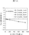
図12には、バイアス周波数が400KHzの場合のフィルタからヒータまでの同軸ケーブル長Lとウエハ上の直流電位差の関係を示す。図には、フィルタのインダクタンスが、1mH、3mH、5mH、および10mHの各状態が示されている(以下の例も同じ)。この図から、バイアス周波数が400KHzの場合には、同軸ケーブル長Lが90m以下であれば、フィルタのインダクタンスの大小に拘わらず、電位差を3.2V以下に抑えることが可能であることがわかる。 FIG. 12 shows the relationship between the coaxial cable length L from the filter to the heater and the DC potential difference on the wafer when the bias frequency is 400 KHz. In the figure, each state of the inductance of the filter is 1 mH, 3 mH, 5 mH, and 10 mH (the following examples are also the same). From this figure, it is understood that when the bias frequency is 400 KHz, the potential difference can be suppressed to 3.2 V or less regardless of the filter inductance if the coaxial cable length L is 90 m or less.
一方、先に述べたとおり、同軸ケーブル長Lは、静電チャックの裏面と電流端子の真空チャンバ内側の端子間の同軸ケーブル(長さ=L1)を含んでいる。この真空チャンバ内側の同軸ケーブル長さL1は、通常、1m以内、例えば50cm〜80cm程度である。また、フィルタは真空チャンバの外側に設置される。換言すると、同軸ケーブル長Lの下限値は、真空チャンバ内側の同軸ケーブル長さL1に真空チャンバ外のフィルタまでのケーブル長を加えたものであり、1m程度である。 On the other hand, as described above, the coaxial cable length L includes the coaxial cable (length = L1) between the back surface of the electrostatic chuck and the terminal inside the vacuum chamber of the current terminal. The coaxial cable length L1 inside the vacuum chamber is usually within 1 m, for example, about 50 cm to 80 cm. The filter is installed outside the vacuum chamber. In other words, the lower limit value of the coaxial cable length L is obtained by adding the cable length to the filter outside the vacuum chamber to the coaxial cable length L1 inside the vacuum chamber, and is about 1 m.
図13には、バイアス周波数が800KHzの場合のフィルタからヒータまでのケーブル長Lとウエハ上の直流電位差の関係を示す。この図から、バイアス周波数が800KHzの場合には、ケーブル長Lが20m以下であれば、電位差を3.2V以下に抑えることが可能であることがわかる。同軸ケーブル長Lの下限値は、真空チャンバ内側の同軸ケーブル長さL1に真空チャンバ外のフィルタまでのケーブル長を加えたものであり、1m程度である。 FIG. 13 shows the relationship between the cable length L from the filter to the heater and the DC potential difference on the wafer when the bias frequency is 800 KHz. From this figure, it is understood that when the bias frequency is 800 KHz, the potential difference can be suppressed to 3.2 V or less if the cable length L is 20 m or less. The lower limit value of the coaxial cable length L is obtained by adding the cable length to the filter outside the vacuum chamber to the coaxial cable length L1 inside the vacuum chamber, and is about 1 m.
図14には、バイアス周波数が2MHzの場合のフィルタからヒータまでのケーブル長Lとウエハ上の直流電位差の関係を示す。この図から、バイアス周波数が2MHzの場合には、ケーブル長Lが3m以下であれば、電位差を3.2V以下に抑えることが可能であることがわかる。同軸ケーブル長Lの下限値は、真空チャンバ内側の同軸ケーブル長さL1に真空チャンバ外のフィルタまでのケーブル長を加えたものであり、1m程度である。 FIG. 14 shows the relationship between the cable length L from the filter to the heater and the DC potential difference on the wafer when the bias frequency is 2 MHz. From this figure, it can be seen that when the bias frequency is 2 MHz, the potential difference can be suppressed to 3.2 V or less if the cable length L is 3 m or less. The lower limit value of the coaxial cable length L is obtained by adding the cable length to the filter outside the vacuum chamber to the coaxial cable length L1 inside the vacuum chamber, and is about 1 m.
図15には、バイアス周波数が13.56MHzの場合のフィルタからヒータまでのケーブル長Lとウエハ上の直流電位差の関係を示す。この図から、バイアス周波数が13.56MHzの場合には、ケーブル長Lが逆に10m以上であれば、電位差を3.2V以下に抑えることが可能であることがわかる。ただ、ケーブル長Lを余り長くしてもその効果に大きな差はない。従って、同軸ケーブル長Lの上限値は、10mを超えた長さでかつフィルタのインダクタンスとの関係で最適な範囲、換言すると10数mである。 FIG. 15 shows the relationship between the cable length L from the filter to the heater and the DC potential difference on the wafer when the bias frequency is 13.56 MHz. From this figure, it can be seen that when the bias frequency is 13.56 MHz, the potential difference can be suppressed to 3.2 V or less if the cable length L is 10 m or more. However, even if the cable length L is too long, there is no significant difference in the effect. Therefore, the upper limit value of the coaxial cable length L is a length exceeding 10 m and an optimum range in relation to the inductance of the filter, in other words, 10 or more m.
以上の見積もりは、本実施例で開示した範囲の構成のヒータ内蔵静電チャックにおいて、最もウエハ上で電位差を生じさせやすい条件での見積もりであるので、逆に言えば各バイアス周波数に応じて同軸ケーブルの長さLを規定してやることにより、いかなる場合にもダメージを引き起こすような電位差が発生することがないといえる。また、静電チャックの給電ケーブルもウエハ上の電位には影響をするが、同一の面積をもつ静電チャック電極に接続された場合には、ヒータのケーブルの長さLの違いはウエハ電位に影響を及ぼさない。 The above estimation is based on the conditions that most easily cause a potential difference on the wafer in the heater built-in electrostatic chuck having the configuration disclosed in the present embodiment. By prescribing the length L of the cable, it can be said that there is no potential difference that causes damage in any case. The electrostatic chuck power supply cable also affects the potential on the wafer. However, when connected to an electrostatic chuck electrode having the same area, the difference in the length L of the heater cable depends on the wafer potential. Has no effect.
実際に、400KHzの周波数でウエハ面内の電位差が3.2V以上となる条件でウエハを処理したときのダメージの発生マップ(a)と、本実施例のケーブル長でウエハ面内の電位差を3.2V以下に押さえて処理したときのダメージの発生マップ(b)を比較したのが図16である。 Actually, the damage generation map (a) when the wafer is processed under the condition that the potential difference in the wafer surface is 3.2 V or more at a frequency of 400 KHz, and the potential difference in the wafer surface is 3 by the cable length of this embodiment. FIG. 16 shows a comparison of damage occurrence maps (b) when processing is performed at a voltage of 2 V or less.
この結果からわかるように、本実施例の条件を満たすケーブルでウエハをエッチング処理した場合にはダメージが発生していないことがわかる。 As can be seen from this result, no damage has occurred when the wafer is etched with a cable that satisfies the conditions of the present embodiment.
以上のように、バイアス周波数毎に適正な長さLに規定された同軸ケーブルでヒータとフィルタ間を接続したプラズマ処理装置においては、仮に双極型静電チャックにおいて内ヒータの一部が一対の静電チャック電極間の環状の隙間から覗くように配置されていたとしても、プラズマ処理中のウエハ面内に電位差を発生させることなくヒータに電力を投入することが可能となる。 As described above, in a plasma processing apparatus in which a heater and a filter are connected with a coaxial cable defined to have an appropriate length L for each bias frequency, a part of the inner heater is assumed to be a pair of static electricity in a bipolar electrostatic chuck. Even if it is arranged so as to look through the annular gap between the electric chuck electrodes, it is possible to supply power to the heater without generating a potential difference in the wafer surface during plasma processing.
そのため、ヒータ内蔵静電チャックのヒータに起因するダメージを発生させることなく、応答性よく温度分布を調節しながらプラズマ処理することができるので、半導体デバイスの製造コストが低く生産性の高いプラズマ処理装置を提供することができる。 Therefore, plasma processing can be performed while adjusting the temperature distribution with high responsiveness without causing damage due to the heater of the electrostatic chuck with built-in heater. Can be provided.
本実施例では、誘電体膜の抵抗率を1×10¹⁵Ωcm以上の高抵抗膜とし、吸着力はいわゆるクーロン力を発生するタイプを採用した。しかし、必ずしもこれに限定されるわけではなく、抵抗率が1×10⁹から1×10¹²Ωcm程度で吸着力を発生させる、いわゆるジョンソン・ラーベック型の静電チャックであってもよい。また、絶縁層や誘電体膜の材質はアルミナを主原料としたが、必ずしもこれに限定されるわけではなく、例えばイットリアや炭化ケイ素、窒化アルミなどの材料であってもよい。 In this embodiment, a dielectric film having a high resistivity of 1 × 10 15 Ωcm or more and a so-called coulomb force is used as the adsorption force. However, the present invention is not necessarily limited thereto, and a so-called Johnson-Rahbek type electrostatic chuck that generates an attractive force with a resistivity of about 1 × 10 9 to 1 × 10 12 Ωcm may be used. In addition, although the material of the insulating layer and the dielectric film is mainly made of alumina, it is not necessarily limited thereto, and may be a material such as yttria, silicon carbide, or aluminum nitride.
また、本実施例では基材の材質としてはチタンを利用しているが、これに限定されるわけではなく他の金属、例えばアルミニウムやアルミニウム合金、ステンレス合金などの金属を利用することも可能である。また、本実施例では静電チャックを溶射法で形成したが必ずしもこの方法に限定される必要はない。ほぼ同様の構成を、内部にヒータ、静電チャック電極を入れ込み焼結法で形成した板状の部材を接着材により本実施例の基材に接着したものであってもよい。この場合、本実施例の積層膜ほどに薄い焼結体セラミックスを形成することは困難であり、多少全体の厚みは増すことになるが、ヒータの熱の伝導の仕方、静電チャックの吸着力の発生の仕方を考慮すれば、本実施例の最下層の絶縁層に相当する部分が厚くなる程度の差で実現可能で、本実施例の技術思想を同様に適用することができる。 Further, in this embodiment, titanium is used as the material of the base material, but the present invention is not limited to this, and other metals such as aluminum, aluminum alloys, and stainless alloys can also be used. is there. In this embodiment, the electrostatic chuck is formed by a thermal spraying method, but it is not necessarily limited to this method. A plate-like member formed by a sintering method in which a heater and an electrostatic chuck electrode are inserted inside may be bonded to the base material of this embodiment with an adhesive. In this case, it is difficult to form a sintered ceramic as thin as the laminated film of this example, and the overall thickness will increase somewhat. However, the heat conduction method of the heater and the adsorption force of the electrostatic chuck In consideration of the manner of occurrence of this, it can be realized with a difference that the portion corresponding to the lowermost insulating layer of this embodiment becomes thick, and the technical idea of this embodiment can be similarly applied.
また、本実施例では内蔵したヒータの系統数は2系統としたが必ずしもこれに限定されるわけではなく、1系統であってもよいし、3系統以上であってもよい。必要な温度分布や実現しなければならない温度の応答性により適宜選択すればよい。また、本実施例の各ヒータのターン数やパターンは必ずしもこれに限定されるべきものではなく、実現したい温度分布や温度の応答性を勘案して適宜決定すべきものである。 Further, in the present embodiment, the number of the built-in heater systems is two, but is not necessarily limited to this, and may be one system or three or more systems. What is necessary is just to select suitably by required temperature distribution and the responsiveness of the temperature which must be implement | achieved. Further, the number of turns and the pattern of each heater in the present embodiment are not necessarily limited to this, and should be appropriately determined in consideration of the temperature distribution and temperature responsiveness to be realized.
1:真空処理室
2: 基材
3:真空チャンバ
4:導波管
5:マイクロ波
6:コイル
7:プラズマ
8:静電チャック
9:ウエハ
10:高周波電源
11:直流電源
12:真空ポンプ
13:処理ガス
14:石英窓
15:バルブ
16:ヘリウム貫通穴
17:フィルタ
18:コンデンサ
19:マイクロ波発振器
20:内ヒータ
21:ケーブル
22:外ヒータ
23:セラミックスパイプ
24:内側静電チャック電極
25:外側静電チャック電極
27:フィルタ
28:誘電体膜
29:同軸ケーブル
30:給電貫通穴
31:冷媒溝
32:プッシャピン用貫通穴
33:ヒータ給電端子接続部
34:電気プラグ
35:高抵抗アルミナ
36:同軸ケーブル
37:同軸ケーブル
38:ヒータ電源
39:高抵抗アルミナ
40:同軸ケーブル
51:可変コンデンサ
52:抵抗
53:同軸ケーブル
54:電流導入端子
80:試料台
C41:内ヒータと基材間の静電容量
C42:外ヒータと基材間の静電容量
C43:内ヒータと内側静電チャック電極間の静電容量
C44:外ヒータと外側静電チャック電極間の静電容量
C45:内側静電チャック電極上の静電容量
C46:外側静電チャック電極上の静電容量
C47:内側静電チャック電極給電ケーブルの静電容量
C48:外側静電チャック電極給電ケーブルの静電容量
C49:内ヒータ給電ケーブルの静電容量
C50:外ヒータ給電ケーブルの静電容量。
1: Vacuum processing chamber 2: Base material 3: Vacuum chamber 4: Waveguide 5: Microwave 6: Coil 7: Plasma 8: Electrostatic chuck 9: Wafer 10: High frequency power source 11: DC power source 12: Vacuum pump 13: Process gas 14: Quartz window 15: Valve 16: Helium through hole 17: Filter 18: Capacitor 19: Microwave oscillator 20: Inner heater 21: Cable 22: Outer heater 23: Ceramic pipe 24: Inner electrostatic chuck electrode 25: Outer Electrostatic chuck electrode 27: Filter 28: Dielectric film 29: Coaxial cable 30: Feeding through hole 31: Refrigerant groove 32: Pusher pin through hole 33: Heater feeding terminal connection 34: Electric plug 35: High resistance alumina 36: Coaxial Cable 37: Coaxial cable 38: Heater power supply 39: High resistance alumina 40: Coaxial cable 51: Variable capacitor 52: Resistance 53: Coaxial cable 54: Current introduction terminal 80: Sample stage C41: Capacitance between the inner heater and the substrate C42: Capacitance between the outer heater and the substrate C43: Static between the inner heater and the inner electrostatic chuck electrode Capacitance C44: Capacitance between the outer heater and the outer electrostatic chuck electrode C45: Capacitance on the inner electrostatic chuck electrode C46: Capacitance on the outer electrostatic chuck electrode C47: Inner electrostatic chuck electrode feeding cable Capacitance C48 of the outer electrostatic chuck electrode power supply cable C49: electrostatic capacity of the inner heater power supply cable C50: electrostatic capacity of the outer heater power supply cable.
Claims (10)
前記ヒータは通電経路を介してヒータ用の電源に接続されており、
高周波の電力が、前記ヒータの通電経路に流れ込むことを抑止する抑止手段を備えていることを特徴とするプラズマ処理装置。 A sample stage installed in the processing chamber and capable of holding a sample, a plasma generating means for generating plasma in the processing chamber, an electrostatic chuck electrode and a heater disposed in the sample stage, and connected to the sample stage In a plasma processing apparatus having a bias power source for ion energy control and a decompression means for decompressing the processing chamber,
The heater is connected to a power source for the heater via an energization path,
A plasma processing apparatus, comprising: suppression means for suppressing high-frequency power from flowing into the energization path of the heater.
前記ヒータ内蔵型静電チャックは、基材の上に積層されたヒータと静電チャック電極及び誘電体膜を有しており、
前記ヒータは前記静電チャック用電極の下側に、該静電チャック用電極に完全に隠れるようにして設けられていることを特徴とするプラズマ処理装置。 A sample stage installed in the processing chamber and capable of holding a sample, a plasma generating means for generating plasma in the processing chamber, a heater built-in electrostatic chuck disposed in the sample stage, and connected to the sample stage In a plasma processing apparatus having a bias power source for ion energy control and a decompression means for decompressing the processing chamber,
The heater built-in electrostatic chuck has a heater laminated on a substrate, an electrostatic chuck electrode, and a dielectric film.
The plasma processing apparatus, wherein the heater is provided below the electrostatic chuck electrode so as to be completely hidden by the electrostatic chuck electrode.
前記ヒータ内蔵型静電チャックは、高周波のバイアス電圧が印加される導電性の基材の上に積層された少なくとも2系統のヒータ、実質的に同一の面積を有する一対の静電チャック電極、及び誘電体膜を有しており、
前記少なくとも2系統のヒータは前記各チャック用電極の下側に、該静電チャック用電極に完全に隠れるようにして設けられていることを特徴とするプラズマ処理装置。 In claim 4,
The heater built-in electrostatic chuck includes at least two systems of heaters laminated on a conductive base material to which a high-frequency bias voltage is applied, a pair of electrostatic chuck electrodes having substantially the same area, and Having a dielectric film,
The plasma processing apparatus, wherein the at least two systems of heaters are provided under the chuck electrodes so as to be completely hidden by the electrostatic chuck electrodes.
前記ヒータ内蔵型静電チャックは、高周波のバイアス電圧が印加される導電性の基材の上に積層された少なくとも2系統のヒータと一対の静電チャック電極を有しており、
前記ヒータは、高周波の電力が前記ヒータの通電経路に流れ込むことを抑止するローパスフィルタ及び同軸ケーブルを介してヒータ用の電源に接続されており、
前記試料台の静電チャック裏面と前記フィルタ間を接続する前記同軸ケーブルの長さが、所定の範囲に設定されていることを特徴とするプラズマ処理装置。 A sample stage installed in the processing chamber and capable of holding a sample, plasma generating means for generating plasma in the processing chamber, a heater built-in electrostatic chuck disposed in the sample stage, and a reduced pressure for depressurizing the processing chamber A plasma processing apparatus comprising:
The heater built-in electrostatic chuck has at least two systems of heaters and a pair of electrostatic chuck electrodes laminated on a conductive base material to which a high-frequency bias voltage is applied.
The heater is connected to a power source for the heater via a low-pass filter and a coaxial cable that prevent high-frequency power from flowing into the energization path of the heater,
The plasma processing apparatus, wherein a length of the coaxial cable connecting the back surface of the electrostatic chuck of the sample stage and the filter is set within a predetermined range.
Priority Applications (2)
| Application Number | Priority Date | Filing Date | Title |
|---|---|---|---|
| JP2008004414A JP2009170509A (en) | 2008-01-11 | 2008-01-11 | Plasma processing apparatus including electrostatic chuck with built-in heater |
| US12/073,082 US20090178764A1 (en) | 2008-01-11 | 2008-02-29 | Plasma processing apparatus including electrostatic chuck with built-in heater |
Applications Claiming Priority (1)
| Application Number | Priority Date | Filing Date | Title |
|---|---|---|---|
| JP2008004414A JP2009170509A (en) | 2008-01-11 | 2008-01-11 | Plasma processing apparatus including electrostatic chuck with built-in heater |
Publications (1)
| Publication Number | Publication Date |
|---|---|
| JP2009170509A true JP2009170509A (en) | 2009-07-30 |
Family
ID=40849649
Family Applications (1)
| Application Number | Title | Priority Date | Filing Date |
|---|---|---|---|
| JP2008004414A Pending JP2009170509A (en) | 2008-01-11 | 2008-01-11 | Plasma processing apparatus including electrostatic chuck with built-in heater |
Country Status (2)
| Country | Link |
|---|---|
| US (1) | US20090178764A1 (en) |
| JP (1) | JP2009170509A (en) |
Cited By (22)
| Publication number | Priority date | Publication date | Assignee | Title |
|---|---|---|---|---|
| JP2011176161A (en) * | 2010-02-25 | 2011-09-08 | Hitachi High-Technologies Corp | Plasma processing apparatus and processing method |
| JP2011258614A (en) * | 2010-06-07 | 2011-12-22 | Hitachi High-Technologies Corp | Plasma processing apparatus or sample placing stand |
| WO2013137414A1 (en) * | 2012-03-16 | 2013-09-19 | 株式会社クリエイティブ テクノロジー | Electrostatic chuck device and method for producing same |
| JP2014130908A (en) * | 2012-12-28 | 2014-07-10 | Ngk Spark Plug Co Ltd | Electrostatic chuck |
| JP2015142042A (en) * | 2014-01-29 | 2015-08-03 | 東京エレクトロン株式会社 | Feeding part cover structure and semiconductor manufacturing device |
| JP2016051783A (en) * | 2014-08-29 | 2016-04-11 | 住友大阪セメント株式会社 | Electrostatic chuck device and manufacturing method for the same |
| JP2016178316A (en) * | 2009-12-15 | 2016-10-06 | ラム リサーチ コーポレーションLam Research Corporation | Plasma etching system |
| CN107195568A (en) * | 2016-03-15 | 2017-09-22 | 三星电子株式会社 | Electrostatic chuck and the lining processor including it |
| JP2018501757A (en) * | 2014-12-11 | 2018-01-18 | アプライド マテリアルズ インコーポレイテッドApplied Materials,Incorporated | Electrostatic chuck for high temperature RF applications |
| JP2018506853A (en) * | 2015-02-03 | 2018-03-08 | アプライド マテリアルズ インコーポレイテッドApplied Materials,Incorporated | High temperature chuck for plasma processing systems |
| JP2018056333A (en) * | 2016-09-29 | 2018-04-05 | 日本発條株式会社 | Substrate mounting base and manufacturing method therefor |
| JP2018133502A (en) * | 2017-02-16 | 2018-08-23 | 日本特殊陶業株式会社 | Electrostatic chuck and substrate holding method |
| KR20190029589A (en) | 2016-06-17 | 2019-03-20 | 도카로 가부시키가이샤 | Heating member |
| WO2019102794A1 (en) * | 2017-11-24 | 2019-05-31 | トーカロ株式会社 | Heat-generating member |
| JP2019169653A (en) * | 2018-03-26 | 2019-10-03 | 株式会社日立ハイテクノロジーズ | Plasma processing apparatus |
| JP2020064916A (en) * | 2018-10-16 | 2020-04-23 | 株式会社東芝 | Process unit |
| KR20200136109A (en) * | 2019-05-27 | 2020-12-07 | 주식회사 원익아이피에스 | Substrate support apparatus and substrate process apparatus having the same |
| WO2020262368A1 (en) * | 2019-06-28 | 2020-12-30 | 日本碍子株式会社 | Electrostatic chuck heater |
| KR20210000723A (en) * | 2018-05-17 | 2021-01-05 | 램 리써치 코포레이션 | Electrostatic chuck filter box and mounting bracket |
| KR20210046088A (en) * | 2018-09-17 | 2021-04-27 | 어플라이드 머티어리얼스, 인코포레이티드 | High-Temperature RF Heater Pedestals |
| JP2021515384A (en) * | 2018-02-28 | 2021-06-17 | ミコ セラミックス リミテッド | Electrostatic chuck heater and its manufacturing method |
| WO2023095707A1 (en) * | 2021-11-26 | 2023-06-01 | 東京エレクトロン株式会社 | Electrostatic chuck and plasma processing device |
Families Citing this family (44)
| Publication number | Priority date | Publication date | Assignee | Title |
|---|---|---|---|---|
| US9132436B2 (en) | 2012-09-21 | 2015-09-15 | Applied Materials, Inc. | Chemical control features in wafer process equipment |
| KR102137617B1 (en) * | 2012-10-19 | 2020-07-24 | 도쿄엘렉트론가부시키가이샤 | Plasma processing apparatus |
| US10049948B2 (en) * | 2012-11-30 | 2018-08-14 | Lam Research Corporation | Power switching system for ESC with array of thermal control elements |
| US10256079B2 (en) | 2013-02-08 | 2019-04-09 | Applied Materials, Inc. | Semiconductor processing systems having multiple plasma configurations |
| JP6202720B2 (en) * | 2013-03-29 | 2017-09-27 | 株式会社日立ハイテクノロジーズ | Plasma processing apparatus and plasma processing method |
| JP2015095409A (en) * | 2013-11-13 | 2015-05-18 | 東京エレクトロン株式会社 | Mounting table and plasma processing apparatus |
| JP6219227B2 (en) * | 2014-05-12 | 2017-10-25 | 東京エレクトロン株式会社 | Heater feeding mechanism and stage temperature control method |
| JP6219229B2 (en) * | 2014-05-19 | 2017-10-25 | 東京エレクトロン株式会社 | Heater feeding mechanism |
| JP6442296B2 (en) | 2014-06-24 | 2018-12-19 | 東京エレクトロン株式会社 | Mounting table and plasma processing apparatus |
| US11637002B2 (en) | 2014-11-26 | 2023-04-25 | Applied Materials, Inc. | Methods and systems to enhance process uniformity |
| CN107004628B (en) * | 2014-12-11 | 2020-09-15 | 应用材料公司 | Electrostatic chuck for high temperature RF applications |
| US20160225652A1 (en) | 2015-02-03 | 2016-08-04 | Applied Materials, Inc. | Low temperature chuck for plasma processing systems |
| US9741593B2 (en) | 2015-08-06 | 2017-08-22 | Applied Materials, Inc. | Thermal management systems and methods for wafer processing systems |
| US10504700B2 (en) | 2015-08-27 | 2019-12-10 | Applied Materials, Inc. | Plasma etching systems and methods with secondary plasma injection |
| JP6608444B2 (en) * | 2015-12-28 | 2019-11-20 | 日本碍子株式会社 | Disc heater and heater cooling plate assembly |
| US10504754B2 (en) | 2016-05-19 | 2019-12-10 | Applied Materials, Inc. | Systems and methods for improved semiconductor etching and component protection |
| US9865484B1 (en) | 2016-06-29 | 2018-01-09 | Applied Materials, Inc. | Selective etch using material modification and RF pulsing |
| US10546729B2 (en) | 2016-10-04 | 2020-01-28 | Applied Materials, Inc. | Dual-channel showerhead with improved profile |
| US10431429B2 (en) | 2017-02-03 | 2019-10-01 | Applied Materials, Inc. | Systems and methods for radial and azimuthal control of plasma uniformity |
| US20180233321A1 (en) * | 2017-02-16 | 2018-08-16 | Lam Research Corporation | Ion directionality esc |
| US10943834B2 (en) | 2017-03-13 | 2021-03-09 | Applied Materials, Inc. | Replacement contact process |
| US11276590B2 (en) | 2017-05-17 | 2022-03-15 | Applied Materials, Inc. | Multi-zone semiconductor substrate supports |
| US11276559B2 (en) | 2017-05-17 | 2022-03-15 | Applied Materials, Inc. | Semiconductor processing chamber for multiple precursor flow |
| JP6924618B2 (en) * | 2017-05-30 | 2021-08-25 | 東京エレクトロン株式会社 | Electrostatic chuck and plasma processing equipment |
| US10297458B2 (en) | 2017-08-07 | 2019-05-21 | Applied Materials, Inc. | Process window widening using coated parts in plasma etch processes |
| KR102432857B1 (en) * | 2017-09-01 | 2022-08-16 | 삼성전자주식회사 | plasma processing apparatus and manufacturing method of semiconductor device using the same |
| US10903054B2 (en) | 2017-12-19 | 2021-01-26 | Applied Materials, Inc. | Multi-zone gas distribution systems and methods |
| US11328909B2 (en) | 2017-12-22 | 2022-05-10 | Applied Materials, Inc. | Chamber conditioning and removal processes |
| US10854426B2 (en) | 2018-01-08 | 2020-12-01 | Applied Materials, Inc. | Metal recess for semiconductor structures |
| US10964512B2 (en) | 2018-02-15 | 2021-03-30 | Applied Materials, Inc. | Semiconductor processing chamber multistage mixing apparatus and methods |
| US10319600B1 (en) | 2018-03-12 | 2019-06-11 | Applied Materials, Inc. | Thermal silicon etch |
| US10886137B2 (en) | 2018-04-30 | 2021-01-05 | Applied Materials, Inc. | Selective nitride removal |
| TW202013581A (en) * | 2018-05-23 | 2020-04-01 | 日商東京威力科創股份有限公司 | Plasma treatment device |
| US10892198B2 (en) | 2018-09-14 | 2021-01-12 | Applied Materials, Inc. | Systems and methods for improved performance in semiconductor processing |
| US11049755B2 (en) | 2018-09-14 | 2021-06-29 | Applied Materials, Inc. | Semiconductor substrate supports with embedded RF shield |
| US11417534B2 (en) | 2018-09-21 | 2022-08-16 | Applied Materials, Inc. | Selective material removal |
| US11682560B2 (en) | 2018-10-11 | 2023-06-20 | Applied Materials, Inc. | Systems and methods for hafnium-containing film removal |
| US11121002B2 (en) | 2018-10-24 | 2021-09-14 | Applied Materials, Inc. | Systems and methods for etching metals and metal derivatives |
| US11437242B2 (en) | 2018-11-27 | 2022-09-06 | Applied Materials, Inc. | Selective removal of silicon-containing materials |
| US11721527B2 (en) | 2019-01-07 | 2023-08-08 | Applied Materials, Inc. | Processing chamber mixing systems |
| US10920319B2 (en) | 2019-01-11 | 2021-02-16 | Applied Materials, Inc. | Ceramic showerheads with conductive electrodes |
| JP7071946B2 (en) * | 2019-06-21 | 2022-05-19 | 東京エレクトロン株式会社 | Plasma processing equipment |
| KR102472864B1 (en) * | 2019-08-06 | 2022-12-02 | 주식회사 미코세라믹스 | Electrostatic chucking heater and manufacturing method thereof |
| US20210289973A1 (en) * | 2020-03-20 | 2021-09-23 | Marvin Gaye Bowen | The core cooker |
Citations (6)
| Publication number | Priority date | Publication date | Assignee | Title |
|---|---|---|---|---|
| JPH02122597U (en) * | 1989-03-15 | 1990-10-08 | ||
| JPH08138891A (en) * | 1994-11-09 | 1996-05-31 | Hitachi Electron Eng Co Ltd | Lower part electrode |
| JPH09106899A (en) * | 1995-10-11 | 1997-04-22 | Anelva Corp | Plasma cvd device and method, and dry etching device and method |
| JPH10144655A (en) * | 1996-11-06 | 1998-05-29 | Sony Corp | Method and apparatus for dry etching |
| JP2003249541A (en) * | 2002-02-26 | 2003-09-05 | Hitachi High-Technologies Corp | Wafer stage |
| JP2007088411A (en) * | 2005-06-28 | 2007-04-05 | Hitachi High-Technologies Corp | Electrostatic attraction device, wafer processing apparatus and plasma processing method |
Family Cites Families (9)
| Publication number | Priority date | Publication date | Assignee | Title |
|---|---|---|---|---|
| JPH09213781A (en) * | 1996-02-01 | 1997-08-15 | Tokyo Electron Ltd | Stage structure and processor using it |
| US7004107B1 (en) * | 1997-12-01 | 2006-02-28 | Applied Materials Inc. | Method and apparatus for monitoring and adjusting chamber impedance |
| US6656838B2 (en) * | 2001-03-16 | 2003-12-02 | Hitachi, Ltd. | Process for producing semiconductor and apparatus for production |
| US20020144786A1 (en) * | 2001-04-05 | 2002-10-10 | Angstron Systems, Inc. | Substrate temperature control in an ALD reactor |
| JP4129855B2 (en) * | 2001-12-13 | 2008-08-06 | 東京エレクトロン株式会社 | Plasma processing equipment |
| US6646233B2 (en) * | 2002-03-05 | 2003-11-11 | Hitachi High-Technologies Corporation | Wafer stage for wafer processing apparatus and wafer processing method |
| JP2006236867A (en) * | 2005-02-25 | 2006-09-07 | Ngk Insulators Ltd | Plasma treatment member |
| US7777152B2 (en) * | 2006-06-13 | 2010-08-17 | Applied Materials, Inc. | High AC current high RF power AC-RF decoupling filter for plasma reactor heated electrostatic chuck |
| JP5301812B2 (en) * | 2007-11-14 | 2013-09-25 | 東京エレクトロン株式会社 | Plasma processing equipment |
-
2008
- 2008-01-11 JP JP2008004414A patent/JP2009170509A/en active Pending
- 2008-02-29 US US12/073,082 patent/US20090178764A1/en not_active Abandoned
Patent Citations (6)
| Publication number | Priority date | Publication date | Assignee | Title |
|---|---|---|---|---|
| JPH02122597U (en) * | 1989-03-15 | 1990-10-08 | ||
| JPH08138891A (en) * | 1994-11-09 | 1996-05-31 | Hitachi Electron Eng Co Ltd | Lower part electrode |
| JPH09106899A (en) * | 1995-10-11 | 1997-04-22 | Anelva Corp | Plasma cvd device and method, and dry etching device and method |
| JPH10144655A (en) * | 1996-11-06 | 1998-05-29 | Sony Corp | Method and apparatus for dry etching |
| JP2003249541A (en) * | 2002-02-26 | 2003-09-05 | Hitachi High-Technologies Corp | Wafer stage |
| JP2007088411A (en) * | 2005-06-28 | 2007-04-05 | Hitachi High-Technologies Corp | Electrostatic attraction device, wafer processing apparatus and plasma processing method |
Cited By (44)
| Publication number | Priority date | Publication date | Assignee | Title |
|---|---|---|---|---|
| US10056225B2 (en) | 2009-12-15 | 2018-08-21 | Lam Research Corporation | Adjusting substrate temperature to improve CD uniformity |
| JP2016178316A (en) * | 2009-12-15 | 2016-10-06 | ラム リサーチ コーポレーションLam Research Corporation | Plasma etching system |
| JP2011176161A (en) * | 2010-02-25 | 2011-09-08 | Hitachi High-Technologies Corp | Plasma processing apparatus and processing method |
| JP2011258614A (en) * | 2010-06-07 | 2011-12-22 | Hitachi High-Technologies Corp | Plasma processing apparatus or sample placing stand |
| WO2013137414A1 (en) * | 2012-03-16 | 2013-09-19 | 株式会社クリエイティブ テクノロジー | Electrostatic chuck device and method for producing same |
| JP2014130908A (en) * | 2012-12-28 | 2014-07-10 | Ngk Spark Plug Co Ltd | Electrostatic chuck |
| JP2015142042A (en) * | 2014-01-29 | 2015-08-03 | 東京エレクトロン株式会社 | Feeding part cover structure and semiconductor manufacturing device |
| JP2016051783A (en) * | 2014-08-29 | 2016-04-11 | 住友大阪セメント株式会社 | Electrostatic chuck device and manufacturing method for the same |
| JP2018501757A (en) * | 2014-12-11 | 2018-01-18 | アプライド マテリアルズ インコーポレイテッドApplied Materials,Incorporated | Electrostatic chuck for high temperature RF applications |
| JP2018506853A (en) * | 2015-02-03 | 2018-03-08 | アプライド マテリアルズ インコーポレイテッドApplied Materials,Incorporated | High temperature chuck for plasma processing systems |
| CN107195568B (en) * | 2016-03-15 | 2021-11-30 | 三星电子株式会社 | Electrostatic chuck and substrate processing apparatus including the same |
| CN107195568A (en) * | 2016-03-15 | 2017-09-22 | 三星电子株式会社 | Electrostatic chuck and the lining processor including it |
| KR20190029589A (en) | 2016-06-17 | 2019-03-20 | 도카로 가부시키가이샤 | Heating member |
| US11272579B2 (en) | 2016-06-17 | 2022-03-08 | Tocalo Co., Ltd. | Heat generating component |
| JP2018056333A (en) * | 2016-09-29 | 2018-04-05 | 日本発條株式会社 | Substrate mounting base and manufacturing method therefor |
| JP2018133502A (en) * | 2017-02-16 | 2018-08-23 | 日本特殊陶業株式会社 | Electrostatic chuck and substrate holding method |
| US11631574B2 (en) | 2017-11-24 | 2023-04-18 | Tocalo Co., Ltd. | Heater component |
| JPWO2019102794A1 (en) * | 2017-11-24 | 2020-07-16 | トーカロ株式会社 | Heating element |
| US12046459B2 (en) | 2017-11-24 | 2024-07-23 | Tocalo Co., Ltd. | Heater component |
| KR20200083517A (en) | 2017-11-24 | 2020-07-08 | 도카로 가부시키가이샤 | Heating element |
| WO2019102794A1 (en) * | 2017-11-24 | 2019-05-31 | トーカロ株式会社 | Heat-generating member |
| KR102398922B1 (en) * | 2017-11-24 | 2022-05-16 | 도카로 가부시키가이샤 | heating element |
| US12040209B2 (en) | 2018-02-28 | 2024-07-16 | Mico Ceramics Ltd. | Electrostatic chuck heater and manufacturing method therefor |
| JP7337064B2 (en) | 2018-02-28 | 2023-09-01 | ミコ セラミックス リミテッド | ELECTROSTATIC CHUCK HEATER AND MANUFACTURING METHOD THEREOF |
| JP2021515384A (en) * | 2018-02-28 | 2021-06-17 | ミコ セラミックス リミテッド | Electrostatic chuck heater and its manufacturing method |
| JP2019169653A (en) * | 2018-03-26 | 2019-10-03 | 株式会社日立ハイテクノロジーズ | Plasma processing apparatus |
| US11398371B2 (en) | 2018-03-26 | 2022-07-26 | Hitachi High-Tech Corporation | Plasma processing apparatus |
| JP7059064B2 (en) | 2018-03-26 | 2022-04-25 | 株式会社日立ハイテク | Plasma processing equipment |
| JP7303830B2 (en) | 2018-05-17 | 2023-07-05 | ラム リサーチ コーポレーション | Electrostatic chuck filter box and mounting bracket |
| KR20210000723A (en) * | 2018-05-17 | 2021-01-05 | 램 리써치 코포레이션 | Electrostatic chuck filter box and mounting bracket |
| KR102661512B1 (en) | 2018-05-17 | 2024-04-25 | 램 리써치 코포레이션 | Electrostatic chuck filter box and mounting bracket |
| JP2021524667A (en) * | 2018-05-17 | 2021-09-13 | ラム リサーチ コーポレーションLam Research Corporation | Electrostatic chuck filter box and mounting bracket |
| KR102586592B1 (en) * | 2018-09-17 | 2023-10-11 | 어플라이드 머티어리얼스, 인코포레이티드 | High Temperature RF Heater Pedestals |
| KR20210046088A (en) * | 2018-09-17 | 2021-04-27 | 어플라이드 머티어리얼스, 인코포레이티드 | High-Temperature RF Heater Pedestals |
| JP7345543B2 (en) | 2018-09-17 | 2023-09-15 | アプライド マテリアルズ インコーポレイテッド | High temperature RF heater pedestal |
| JP2022500862A (en) * | 2018-09-17 | 2022-01-04 | アプライド マテリアルズ インコーポレイテッドApplied Materials, Incorporated | High temperature RF heater pedestal |
| JP7209508B2 (en) | 2018-10-16 | 2023-01-20 | 株式会社東芝 | process equipment |
| JP2020064916A (en) * | 2018-10-16 | 2020-04-23 | 株式会社東芝 | Process unit |
| KR102673943B1 (en) * | 2019-05-27 | 2024-06-11 | 주식회사 원익아이피에스 | Substrate support apparatus and substrate process apparatus having the same |
| KR20200136109A (en) * | 2019-05-27 | 2020-12-07 | 주식회사 원익아이피에스 | Substrate support apparatus and substrate process apparatus having the same |
| JPWO2020262368A1 (en) * | 2019-06-28 | 2020-12-30 | ||
| WO2020262368A1 (en) * | 2019-06-28 | 2020-12-30 | 日本碍子株式会社 | Electrostatic chuck heater |
| JP7522110B2 (en) | 2019-06-28 | 2024-07-24 | 日本碍子株式会社 | Electrostatic Chuck Heater |
| WO2023095707A1 (en) * | 2021-11-26 | 2023-06-01 | 東京エレクトロン株式会社 | Electrostatic chuck and plasma processing device |
Also Published As
| Publication number | Publication date |
|---|---|
| US20090178764A1 (en) | 2009-07-16 |
Similar Documents
| Publication | Publication Date | Title |
|---|---|---|
| JP2009170509A (en) | Plasma processing apparatus including electrostatic chuck with built-in heater | |
| US10332728B2 (en) | Plasma processing apparatus | |
| US9142391B2 (en) | Method of manufacturing semiconductor device | |
| TWI621172B (en) | Plasma treatment device | |
| KR100924855B1 (en) | Loading table for plasma processing apparatus and plasma processing apparatus | |
| US8080126B2 (en) | Plasma processing apparatus | |
| US20180308669A1 (en) | Electrode assembly | |
| US8398815B2 (en) | Plasma processing apparatus | |
| TWI533395B (en) | Plasma processing device and method of manufacturing semiconductor device | |
| JP4482308B2 (en) | Plasma processing apparatus and plasma processing method | |
| TWI488236B (en) | Focusing ring and plasma processing device | |
| US20130112666A1 (en) | Plasma processing apparatus | |
| TW201316399A (en) | Powered grid for plasma chamber | |
| US20100078129A1 (en) | Mounting table for plasma processing apparatus | |
| US9583313B2 (en) | Plasma processing apparatus and plasma processing method | |
| TWI734185B (en) | Plasma processing apparatus | |
| JP2015162266A (en) | plasma processing apparatus | |
| KR102586592B1 (en) | High Temperature RF Heater Pedestals | |
| TW201342508A (en) | Radio frequency filter for electrostatic chuck | |
| JP2007067036A (en) | Vacuum processing device | |
| CN107546095A (en) | Support component, the apparatus and method for handling substrate | |
| TW201407714A (en) | Plasma processing apparatus | |
| JP2007250860A (en) | Plasma processor and electrode assembly therefor | |
| JP2006165093A (en) | Plasma processing device | |
| TWI701706B (en) | Plasma processing apparatus |
Legal Events
| Date | Code | Title | Description |
|---|---|---|---|
| A621 | Written request for application examination |
Free format text: JAPANESE INTERMEDIATE CODE: A621 Effective date: 20101220 |
|
| A977 | Report on retrieval |
Free format text: JAPANESE INTERMEDIATE CODE: A971007 Effective date: 20110826 |
|
| A131 | Notification of reasons for refusal |
Free format text: JAPANESE INTERMEDIATE CODE: A131 Effective date: 20121106 |
|
| A02 | Decision of refusal |
Free format text: JAPANESE INTERMEDIATE CODE: A02 Effective date: 20130305 |