JP5618638B2 - Plasma processing equipment or sample mounting table - Google Patents
Plasma processing equipment or sample mounting table Download PDFInfo
- Publication number
- JP5618638B2 JP5618638B2 JP2010129522A JP2010129522A JP5618638B2 JP 5618638 B2 JP5618638 B2 JP 5618638B2 JP 2010129522 A JP2010129522 A JP 2010129522A JP 2010129522 A JP2010129522 A JP 2010129522A JP 5618638 B2 JP5618638 B2 JP 5618638B2
- Authority
- JP
- Japan
- Prior art keywords
- wafer
- heater
- temperature
- film
- dielectric film
- Prior art date
- Legal status (The legal status is an assumption and is not a legal conclusion. Google has not performed a legal analysis and makes no representation as to the accuracy of the status listed.)
- Active
Links
Images


Classifications
-
- C—CHEMISTRY; METALLURGY
- C23—COATING METALLIC MATERIAL; COATING MATERIAL WITH METALLIC MATERIAL; CHEMICAL SURFACE TREATMENT; DIFFUSION TREATMENT OF METALLIC MATERIAL; COATING BY VACUUM EVAPORATION, BY SPUTTERING, BY ION IMPLANTATION OR BY CHEMICAL VAPOUR DEPOSITION, IN GENERAL; INHIBITING CORROSION OF METALLIC MATERIAL OR INCRUSTATION IN GENERAL
- C23C—COATING METALLIC MATERIAL; COATING MATERIAL WITH METALLIC MATERIAL; SURFACE TREATMENT OF METALLIC MATERIAL BY DIFFUSION INTO THE SURFACE, BY CHEMICAL CONVERSION OR SUBSTITUTION; COATING BY VACUUM EVAPORATION, BY SPUTTERING, BY ION IMPLANTATION OR BY CHEMICAL VAPOUR DEPOSITION, IN GENERAL
- C23C28/00—Coating for obtaining at least two superposed coatings either by methods not provided for in a single one of groups C23C2/00 - C23C26/00 or by combinations of methods provided for in subclasses C23C and C25C or C25D
-
- C—CHEMISTRY; METALLURGY
- C23—COATING METALLIC MATERIAL; COATING MATERIAL WITH METALLIC MATERIAL; CHEMICAL SURFACE TREATMENT; DIFFUSION TREATMENT OF METALLIC MATERIAL; COATING BY VACUUM EVAPORATION, BY SPUTTERING, BY ION IMPLANTATION OR BY CHEMICAL VAPOUR DEPOSITION, IN GENERAL; INHIBITING CORROSION OF METALLIC MATERIAL OR INCRUSTATION IN GENERAL
- C23C—COATING METALLIC MATERIAL; COATING MATERIAL WITH METALLIC MATERIAL; SURFACE TREATMENT OF METALLIC MATERIAL BY DIFFUSION INTO THE SURFACE, BY CHEMICAL CONVERSION OR SUBSTITUTION; COATING BY VACUUM EVAPORATION, BY SPUTTERING, BY ION IMPLANTATION OR BY CHEMICAL VAPOUR DEPOSITION, IN GENERAL
- C23C4/00—Coating by spraying the coating material in the molten state, e.g. by flame, plasma or electric discharge
- C23C4/02—Pretreatment of the material to be coated, e.g. for coating on selected surface areas
Landscapes
- Chemical & Material Sciences (AREA)
- Engineering & Computer Science (AREA)
- Organic Chemistry (AREA)
- Materials Engineering (AREA)
- Mechanical Engineering (AREA)
- Metallurgy (AREA)
- Chemical Kinetics & Catalysis (AREA)
- Physics & Mathematics (AREA)
- Plasma & Fusion (AREA)
- Container, Conveyance, Adherence, Positioning, Of Wafer (AREA)
- Drying Of Semiconductors (AREA)
- Plasma Technology (AREA)
- Control Of Resistance Heating (AREA)
- Resistance Heating (AREA)
Description
本発明は、真空容器内の処理室内に配置されたウエハを処理室内に発生させたプラズマを用いて処理するプラズマ処理装置に関して、処理室内に置かれた処理台の温度を調節してウエハの温度を処理に適した温度に調整しつつこれを処理するプラズマ処理装置に関する。 The present invention relates to a plasma processing apparatus for processing a wafer disposed in a processing chamber in a vacuum chamber using plasma generated in the processing chamber, and adjusting the temperature of a processing table placed in the processing chamber to adjust the temperature of the wafer. It is related with the plasma processing apparatus which processes this, adjusting this to the temperature suitable for a process.
このようなプラズマ処理装置において、半導体ウエハ等の基板状の試料の表面に形成された複数の処理対象の膜が複数積層されている所謂多層膜を処理する時間を短縮するために、上下に隣り合う膜を同一の処理室内部で且つこれらの膜の各々の処理の間に処理室外にウエハを取り出すことなく処理することが考えられている。また、従来より、より微細な加工を高い精度で行うことが求められており、処理対象の膜をエッチング等の加工処理した結果の形状のウエハの面方向(径方向,周方向)について均一性を高くするために、処理対象の各膜においてその加工に適切なものになるようにウエハの温度を調節することが行われてきた。 In such a plasma processing apparatus, in order to shorten the time for processing a so-called multilayer film in which a plurality of processing target films formed on the surface of a substrate-like sample such as a semiconductor wafer are stacked, it is adjacent to the upper and lower sides. It is conceivable to process matching films within the same processing chamber and without removing the wafer out of the processing chamber between each processing of these films. Conventionally, it has been demanded to perform finer processing with high accuracy, and uniformity in the surface direction (radial direction, circumferential direction) of the wafer as a result of processing the film to be processed, such as etching. In order to increase the temperature, the wafer temperature has been adjusted so that each film to be processed is suitable for processing.
このような温度の調節する技術としては、たとえば特許文献1に開示されるように、ウエハが載せられる面を構成する試料載置台の上部をセラミック製の円板状の部材及びこれに接続されて下方に配置された加熱器を配置し、加熱器の発熱量を調節して、セラミック製の円板及びその上面に載せられるウエハの温度を加工するのに適したものにするものが知られている。特に、特許文献1では、セラミック製の円板状の部材はその内部にはウエハをその上面に吸着させる静電気力を形成するために直流電力が供給される電極が内蔵されており、円板状の部材の下面に所定の厚さで膜状のヒータが形成され、さらにその周囲を樹脂製の接着剤で覆い、円板状部材の接着剤が付された側部分を接着剤を挟んで試料載置台の導電体製の本体の上面に押しつけて接合して試料載置台を構成するものが開示されている。
As a technique for adjusting the temperature, as disclosed in, for example,
ヒータは金属や耐熱性の樹脂内に導電性材料や半導体材料を混入して形成した材料が用いられ、試料載置台本体の内部に配置された貫通孔の内部に配置されたコネクターにより電力が供給される。また、試料載置台の中心側と外周側との2つの領域の各々に異なるコネクターを介して異なる大きさの電力が供給されるように構成され、試料載置台及びその上方に載せられるウエハの温度を中心側部分と外周側部分とで異なる分布を得られるように構成されている。 The heater is made of a metal or heat-resistant resin mixed with a conductive material or semiconductor material, and power is supplied by a connector placed inside a through-hole placed inside the sample mounting base. Is done. In addition, each of the two regions on the center side and the outer periphery side of the sample mounting table is configured to be supplied with electric power of different magnitudes via different connectors, and the temperature of the sample mounting table and the wafer mounted thereon Can be obtained so that different distributions can be obtained in the central portion and the outer peripheral portion.
上記の従来技術の試料載置台においては、処理に適したウエハの温度の分布の精度や温度の均一性を向上させるため、試料載置台の表面のセラミック製の円板状の部材内部に設置されたヒータは複数のエリアに分割され、各エリアで円盤状の部材の表面の温度を所望のものとするようにヒータの発熱量が調節されている。また、複数のヒータが配置される載置面上に区分けされた各エリアでのヒータの発熱量の不均一を解消し、ウエハの面方向についての温度の均一性を向上させるため、試料載置台の表面のセラミック製の円板状の部材の厚さを大きくして、熱容量を大きくして均熱効果を持たせて温度の高低差の大きさを小さくすることや、セラミック製の円板状部材の内部に熱伝導率の高い材料、例えば金属製の板状の部材を配置してこの板部材が熱の伝達の量大きくすることにより、円板状の部材の表面で生じる温度差を低減してウエハの温度の均一性を向上することが行われている。 In the above-described conventional sample mounting table, in order to improve the temperature distribution accuracy and temperature uniformity suitable for processing, the sample mounting table is installed inside a ceramic disk-shaped member on the surface of the sample mounting table. The heater is divided into a plurality of areas, and the heating value of the heater is adjusted so that the surface temperature of the disk-shaped member is desired in each area. In addition, in order to eliminate unevenness in the amount of heat generated by the heaters in each area divided on the mounting surface on which a plurality of heaters are arranged, and to improve temperature uniformity in the wafer surface direction, the sample mounting table Increase the thickness of the ceramic disk-shaped member on the surface of the surface to increase the heat capacity and have a soaking effect to reduce the temperature difference, or the ceramic disk-shaped A material with high thermal conductivity, for example, a metal plate-like member is placed inside the member, and this plate member increases the amount of heat transfer, thereby reducing the temperature difference generated on the surface of the disk-like member. Thus, the uniformity of the temperature of the wafer is improved.
また、ヒータの発熱の量を調節する場合基準となる温度を検出する必要があるが、直接ウエハ温度を精度よく測定することが難しいことから、上記従来技術では試料載置台上部の基材を構成する金属製の部材の内部であってヒータの近傍に温度センサ等の検知手段を配置して、この検知手段の出力から検出される温度を用いて、ウエハ或いは試料載置台の表面の温度を所望の値の範囲となるようにヒータへ供給される電力や発熱の量が調節されている。 In addition, it is necessary to detect the reference temperature when adjusting the amount of heat generated by the heater. However, since it is difficult to accurately measure the wafer temperature directly, the above-mentioned conventional technology constitutes the base material on the upper part of the sample mounting table. A detecting means such as a temperature sensor is arranged in the vicinity of the heater inside the metal member to be used, and the temperature detected from the output of the detecting means is used to determine the surface temperature of the wafer or the sample mounting table. The electric power supplied to the heater and the amount of heat generation are adjusted so as to be in the range of the above values.
しかし、円板状の部材の厚さを大きくしたり、内部に均熱板を設置したりすることによって、ヒータからウエハまでの距離が増加することから、ヒータによって温度変化される熱容量が増加する。このため、例えウエハの加工の際に各膜で最適な温度へ変化させるためにヒータの発熱の量を調節したとしても、この調節した結果がセラミック製の円板状の部材の表面の温度或いはウエハの温度に反映されるまでの応答の時間が増加してしまい、結果として処理中の時間における時刻において適切な温度と実際のウエハの表面の温度との間の差が大きくなって、ハードマスクからメタル層まで一貫で処理する場合にメタル層のCDが細くなる等、加工の精度が低下してしまう虞があった。また、試料載置台内部に設置された温度センサと試料載置台上部に置かれたウエハ間で熱抵抗が増大し、試料載置台内部の温度センサの温度と実際のウエハの温度との差が大きくなり、ウエハの温度の調節の精度が低下してしまうという問題について、上記従来の技術では考慮が不十分であった。 However, by increasing the thickness of the disk-shaped member or installing a soaking plate inside, the distance from the heater to the wafer increases, so the heat capacity that is temperature-changed by the heater increases. . For this reason, even if the amount of heat generated by the heater is adjusted in order to change the temperature to the optimum temperature for each film during wafer processing, the result of this adjustment is the temperature of the surface of the ceramic disk-shaped member or The response time until it is reflected in the wafer temperature increases, and as a result, the difference between the appropriate temperature and the actual wafer surface temperature at the time during processing increases, and the hard mask In the case of consistent processing from the metal layer to the metal layer, there is a possibility that the processing accuracy may be lowered, for example, the CD of the metal layer becomes thin. In addition, the thermal resistance increases between the temperature sensor installed inside the sample mounting table and the wafer placed on the upper part of the sample mounting table, and the difference between the temperature of the temperature sensor inside the sample mounting table and the actual wafer temperature is large. Thus, the above-described conventional technique has not sufficiently considered the problem that the accuracy of adjusting the temperature of the wafer is lowered.
本発明の目的は、ウエハの温度の変化を高速化し温度の調節の精度を向上して処理の効率を向上できるプラズマ処理装置または試料の載置台を提供することにある。 An object of the present invention is to provide a plasma processing apparatus or a sample mounting table capable of improving the efficiency of processing by speeding up the change in temperature of a wafer and improving the accuracy of temperature adjustment.
上記目的は、真空容器内部の処理室内に配置された試料台上にウエハを載置して前記処理室内に形成したプラズマを用いて前記ウエハを処理するプラズマ処理装置であって、前記試料台が、その内部に冷媒流路が配置された金属製の基材と、この基材上面を覆って配置された温度分布均一化層と、この温度分布均一化層上に接着層を介して配置され内部または下面に前記ウエハを吸着・保持するための静電吸着用の電極膜を有した焼結セラミック板と、前記基材内部に配置され温度を検知するセンサと、このセンサからの出力を受けて前記ヒータの発熱を調節する制御部とを備え、前記温度分布均一化層が、前記基材上面に溶射により形成・配置された第1の誘電体膜と、この第1の誘電体膜の上に溶射によって配置され金属材料から構成された膜状のヒータであって単位面積あたりの発熱量が膜全体で均一化されるようにその厚さが調節された膜状のヒータと、前記第1の誘電体膜及び前記ヒータの上方に溶射により形成・配置された第2の誘電体膜とを備えて構成されたことにより達成される。
The above object is a plasma processing apparatus for processing a wafer by using a plasma formed in the processing chamber by placing the wafer on a sample table disposed in the processing chamber inside the vacuum vessel, A metal base material in which a refrigerant flow path is disposed, a temperature distribution uniform layer disposed so as to cover the upper surface of the base material, and an adhesive layer disposed on the temperature distribution uniform layer. A sintered ceramic plate having an electrode film for electrostatic adsorption for adsorbing and holding the wafer inside or under the surface, a sensor arranged inside the substrate for detecting temperature, and receiving an output from the sensor A control unit for adjusting the heat generation of the heater, and the temperature distribution uniformizing layer is formed and arranged on the upper surface of the base material by thermal spraying, and the first dielectric film Composed of metal material placed by thermal spraying on A film-like thickness thereof is adjusted film-like heater, as the amount of heat generated per unit area a heater is uniform throughout the film, above the first dielectric film and the heater This is achieved by including the second dielectric film formed and arranged by thermal spraying.
また、前記第二の誘電体膜は、これを構成する誘電体製の材料が前記第1の誘電体膜及び前記ヒータの上方に溶射によって配置された後に前記ヒータが配置された領域の全体で当該誘電体製の材料の厚さが均等化されるようにその上面の形状が調節されたものであることにより達成される。
In addition, the second dielectric film is formed over the entire region where the heater is disposed after the dielectric material constituting the second dielectric film is disposed above the first dielectric film and the heater by thermal spraying. This is achieved by adjusting the shape of the upper surface so that the thickness of the dielectric material is equalized.
以下、図を用いながら本発明の実施例を説明する。 Embodiments of the present invention will be described below with reference to the drawings.
〔実施例〕
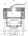
図1は、本発明の係わるプラズマ処理装置の構成の概略を説明する縦断面図である。図1において、プラズマ処理装置100は、真空容器101と、その上方の外周に配置されて真空容器101内部に電界又は磁界を供給する電磁場供給手段と、真空容器101下方に配置されて真空容器101内部を排気する排気手段とを備えている。
〔Example〕
FIG. 1 is a longitudinal sectional view for explaining the outline of the configuration of a plasma processing apparatus according to the present invention. In FIG. 1, a
真空容器101内部には、その内側にプラズマが形成される空間であって内側に配置された処理対象の試料が当該プラズマにより処理される処理室103と、処理室103下部に配置されて試料がその上面に載せられて保持される試料載置台107が備えられている。また、真空容器101上方には、電磁場供給手段としてマイクロ波やUHF波等の所定の周波数の電界を形成するマグネトロン等の電波源104と電波を伝播して処理室103内に導く管路である導波管105と、導波管105と接続されこの内部を伝播してきた電波が導入されて内部の空間で共振する共振容器106とが配置されている。
Inside the
さらに、真空容器の上部のソレノイドコイル113が配置されている。ソレノイドコイル113は、円筒形状の真空容器101の上部の外周を囲んで配置され、これに供給された電流により磁場を発生する。本実施例では、ソレノイドコイル113は複数の段数で配置されており、処理室103内側に上下方向の中心軸の周りに等磁場が軸対象で下向きに末広がりとなる形状の磁界が導入される。
Furthermore, a
また、真空容器101の下方には、排気手段であるターボ分子ポンプ等の真空ポンプ102が配置され、真空容器101内部の処理室102下部で試料載置台107の直下方に配置された円形の排気用の開口と連通している。真空容器101内の処理室103は略円筒形状を備え、その下部の中央部であって前記開口の上方には略円筒形状を有してウエハがその上面に載置される試料載置台107が配置されている。
In addition, a
本実施例では、処理室103,試料載置台107、開口がそれらの軸が合致するように上下に配置されており、また試料載置台107の外側壁と処理室103の内側壁との間の空間も軸が合致したリング形状となっている。なお、試料載置台107は外側壁から水平方向外側に延在する複数の梁で開口の上方で空間を空けて中空に支持されており、これらの梁は試料載置台107の上下方向の中心軸の周囲に軸対象となるように配置されている。
In this embodiment, the
円筒形状の処理室103の上方には、軸を合わせた円筒形状を有する共振容器106内の共振用の空間である共振室106′が配置されている。この共振室106′と処理室103との間は、共振室106′の底面を構成する石英等誘電体製の円板状の窓部材114が配置されて、両者の間を気密に区画している。
Above the
窓部材114の下方には窓部材114の下面とすき間を空けて並列に石英等誘電体製の円板状のシャワープレート115が配置されており、シャワープレート115の下面が処理室103の天井面を構成している。シャワープレート115は試料載置台107の上面と対向して並列に配置されて、その中央部には処理室103内に上方からウエハ処理用のガスが導入される貫通孔が複数配置されている。上記窓部材114とシャワープレート115との間のすき間は、プラズマ処理装置100が設置されるクリーンルーム等建屋に設置された図示しないガス源から供給される処理用ガスが通流する管路が連通されており、ガス源からの処理用のガスは管路を通り上記すき間に導入されて後、貫通孔を通り下方の試料載置台107方向に処理室103内に流入する。
Below the
試料載置台107は、内部に導電体製の電極が配置され、この電極が所定の周波数の高周波電力を出力するバイアス電源108と電気的に接続されている。試料載置台107上面の載置面上にウエハが載せられた状態でこのバイアス電源108から供給された高周波電力によりウエハ表面にバイアス電位が形成され試料載置台107上方の処理室103内に形成されるプラズマとの間の電位差により荷電粒子をウエハ上面に誘引する作用を奏する。
The sample mounting table 107 has an electrode made of a conductor disposed therein, and the electrode is electrically connected to a
さらに、試料載置台107には後述の通り、載置面表面またはウエハの温度を調節するヒータが内部に配置され、このヒータには電力を供給するヒータ電極用直流電源109が電気的に接続されている。また、試料載置台107の上部には試料の載置面を構成するAl2O3やY2O3等の誘電体の材料から構成された誘電体膜が配置されているが、その内部にはウエハを誘電体膜表面上に静電気力により吸着する静電吸着電極が配置されており、この静電吸着電極に直流電力を供給する静電吸着電極用直流電源110が電気的に接続されている。
Further, as will be described later, a heater for adjusting the surface of the mounting surface or the temperature of the wafer is disposed inside the sample mounting table 107, and a
また、試料載置台107はウエハの処理中にプラズマから熱が伝達されて温度が上昇する。処理中に適切な温度となるように調節するために試料載置台107の内部には冷媒が供給されて通流する冷媒通路が試料載置台107の上下方向の中心軸の周りに同心状またはら旋状に配置されている。この冷媒通路の冷媒の入口,出口と連結された冷媒の管路は冷媒の温度調節を行う温調器111が連結されており、試料載置台107内部の冷媒通路及び外部の管路を通り温調器111に流入した冷媒は所定の温度に調節されて再度管路を介して試料載置台107内部の冷媒通路に供給されて循環する。
Further, the temperature of the sample mounting table 107 rises due to heat transferred from the plasma during wafer processing. In order to adjust the temperature to be an appropriate temperature during processing, a coolant passage through which a coolant is supplied and flows inside the sample mounting table 107 is concentric or centered around the central axis in the vertical direction of the sample mounting table 107. Arranged in a spiral. The refrigerant pipe connected to the refrigerant inlet and outlet of the refrigerant passage is connected to a
なお、上記のプラズマ処理装置100の各部は制御部であるコントローラ112と通信手段を介して連結されて、その動作が適切に調節される。コントローラ112は図示しないメモリー等の記憶装置や演算器,通信用コネクター等から構成され、プラズマ処理装置100の複数箇所に配置された検知手段であるセンサからの出力を通信手段を介し受信し、演算器によって算出した指令を上記各部に送信して所期の結果が得られるように動作を調節する。
In addition, each part of said
上記の構成を備えた本実施例では、処理室103内にガス源からアルゴン等の不活性ガスが導入されつつ排気手段により排気されることで減圧された状態で、図示しないロボットアーム等の搬送手段により図示しないゲートを通りウエハが試料載置台107上に搬送されてこれに受け渡される。ウエハは試料載置台107の載置面を構成する誘電体膜上に載せられた後、静電吸着電極用直流電源110から誘電体膜内の電極に電力が供給され静電気力が形成されて誘電体膜上に吸着されて保持される。
In the present embodiment having the above-described configuration, a robot arm or the like (not shown) is transported in a state where an inert gas such as argon is introduced from the gas source into the
ガス源から上記シャワープレート115の貫通孔を通り処理室103内に処理用ガスが導入されつつ、真空ポンプ102の動作による開口からの排気とのバランスにより、処理室103内部の圧力が所定の範囲に調節される。電波源104で形成されたマイクロ波は導波管105内を伝播して共振容器106に到達し所定の強度の電界が内部の共振室106′で形成される。この電界は窓部材114,シャワープレート115を透過して処理室103内に供給される。
While the processing gas is introduced from the gas source through the through hole of the
ソレノイドコイル113から供給された磁場(磁界)と共振容器106から供給された電界との相互作用により、処理用ガスが励起されてプラズマ化され、処理室103内の試料載置台107上方の空間にプラズマが形成される。バイアス電源108からの高周波電力によって形成されたバイアス電位がウエハ表面にプラズマ中の荷電粒子を誘引して、ウエハ表面の処理対象の膜が生起される物理的,化学的反応によってエッチング等の所期の処理が行われる。
Due to the interaction between the magnetic field (magnetic field) supplied from the
本実施例では、プラズマの生成は上記マイクロ波による電界と磁界との相互作用によるECRを用いているが、これに限定されるものではなく、高周波を用いた静電結合手段または誘導結合手段によるプラズマ生成手段を用いても良い。 In the present embodiment, the plasma is generated by using the ECR based on the interaction between the electric field and the magnetic field by the microwave. However, the present invention is not limited to this, but by the electrostatic coupling means or the inductive coupling means using a high frequency. Plasma generating means may be used.
図2は、図1に示す実施例の試料載置台の構成の概略を拡大して示す縦断面図である。本図は、図1において示した試料載置台107の構成をより詳細に示す図である。 FIG. 2 is an enlarged longitudinal sectional view schematically showing the configuration of the sample mounting table of the embodiment shown in FIG. This figure is a diagram showing the configuration of the sample mounting table 107 shown in FIG. 1 in more detail.
試料載置台107は、円板形状を備えAlまたはTi等の金属で構成される基材部201と、基材部201の上面に接合されて配置され、内部にヒータと静電吸着用電極を備えたAl2O3等の誘電体による誘電体膜部202を備えて構成されている。基材部201の内部には上記の通り基材部201を冷却するための冷媒が内部を流れる冷媒通路である冷媒溝203が基材部201の上下方向の中心軸周りに同心状またはら旋状に配置されている。冷媒溝203は冷媒が導入される入口部及び排出される出口部が管路により真空容器101外部の温調器111と連結されており、温調器111が冷媒溝203を通り循環される冷媒の流量(速度)や冷媒の温度をコントローラ112からの指令信号に応じて調節する。
The sample mounting table 107 is provided with a
Al2O3等の誘電体材料により構成された誘電体膜部202の構成について説明する。誘電体膜部202は大きくわけて3つの層に分けられる。上方の層は、その内部に静電吸着用の電極が配置されウエハの載置面を構成する円板状の部材が配置され、下方には、円板形状を有する基材部201の上面には、膜状のヒータを内部に含む複数の層の誘電体材料の膜が配置されている。これら上下の層の間は、両者を接着して接合する接着層が配置されている。
The configuration of the
本実施例では、下方の層の誘電体材料は金属製の基材部201の上面との十分な接合の強度を得るために、溶射法により形成されている。また、膜状のヒータも溶射により形成される。
In the present embodiment, the dielectric material of the lower layer is formed by a thermal spraying method in order to obtain sufficient bonding strength with the upper surface of the
本実施例の上方の層を構成する円板状の部材は、Al2O3やY2O3等のセラミック材料を所定の厚さと径とを有する円板形状に焼成して形成した焼結体である焼結セラミック板209である。焼結セラミック板209の内部には、直流電力が供給されて静電気力を生起する膜状の静電吸着用電極膜208が配置されており、焼結セラミック板209の下面には静電吸着用電極膜208と電気的に接続されたコネクター部が配置され、基材部201上に試料載置台107と接合された状態で静電吸着電極用直流電源110と接続される。
The disk-shaped member constituting the upper layer of this example is a sintered material formed by firing a ceramic material such as Al 2 O 3 or Y 2 O 3 into a disk shape having a predetermined thickness and diameter. It is a sintered
下方の層を構成する誘電体製の膜は、まず基材部201の上にAl2O3等からなる第一誘電体膜204が溶射によって形成された上に、金属材料が溶射法により所定の形状にヒータ電極膜205として形成される。ヒータ電極膜205は、溶射によって第一誘電体膜204上に吹き付けられる際に実現を求められるウエハ又は載置面表面での温度の分布に応じた所定の形状となるようにマスクが用られる。ヒータ電極膜205を形成するため溶射される金属としては、W,抵抗率を制御したニッケル−クロム合金やニッケル−アルミ合金、あるいはWに適当な添加金属を混ぜ抵抗率を制御したものなど抵抗率が管理された金属が用いられる。
The dielectric film constituting the lower layer is formed by firstly spraying a
溶射法によって形成されたこれらの膜は、融解または半融解した材料の微小な粒子が膜により覆われる対象の表面上に吹き付けられて表面と衝突した衝撃で変形した粒子が積み重なって積層されたものである。これらの粒子同士は対象の表面に衝突した際に、粒子の表面が融解した状態で接触して接合され融着し、粒子間には微小な空間が形成されている。このため膨張,収縮等変形によって部材の欠損や割れの発生が生じにくく脆性が相対的に低い。また、膜を形成した後の切削等形状の変更が容易となる。 These films formed by thermal spraying are made by laminating particles that are deformed by impact that collides with the surface by spraying fine particles of molten or semi-melted material on the surface of the object covered by the film It is. When these particles collide with the surface of the object, the particles are in contact with each other in a melted state, joined and fused, and a minute space is formed between the particles. For this reason, it is hard to produce the defect | deletion and a crack of a member by deformation, such as expansion | swelling and contraction, and brittleness is relatively low. In addition, it is easy to change the shape such as cutting after the film is formed.
本実施例では、マスクの形状に合わせてヒータ電極膜205の材料を溶射した後、製膜されたヒータ電極膜205の膜の厚さを各箇所での単位面積あたりの発熱の量が膜全体で均等となるように削って調節する。これにより、ヒータ電極膜208が配置された領域で発熱量が均一化され、ウエハの周方向,径方向についてその温度の分布の不均一が抑制される。
In this embodiment, after the material of the
溶射された第一の誘電体膜204及びヒータ電極膜205上に、再びAl2O3等誘電体材料が溶射によって吹き付けられ第二誘電体膜206が形成される。この後、ヒータ電極膜208の上面と第二誘電体膜206の上面との距離を、ヒータ電極膜208が配置された領域の全体で均等となるように第二誘電体膜206上面を削って調節しても良い。
On the sprayed first
これらの溶射による下方の膜の形成の前に予め、上方の膜である焼結セラミック板209の焼成を別途行う。本実施例では、焼結セラミック板209内部の静電吸着用電極膜208は、上方から見て円形の中心部とこれを囲むリング状の外周部との2つの領域に配置され、それぞれが静電吸着電極用直流電源110と電気的に接続されて異なる値の電力が静電吸着電極用直流電源110から供給される。
Prior to the formation of the lower film by the thermal spraying, the sintered
焼結セラミック板209は、厚さ方向についてその上下をセラッミック材料に挟まれた中間部分である内部にW(タングステン)等の金属から構成される静電吸着用電極膜208が包含されて配置されるとともに、静電吸着用電極膜208を内部に包含して配置された状態で円板形状に成形されたセラミック材が、冷却された状態でその厚さが0.2〜0.4mmの範囲内の値なるように焼結の条件が調節されて焼成される。
The sintered
第二誘電体膜206が所定の形状に成形された後、その上にシリコーン系の接着材207が塗布され、焼結セラミック板209と下方の層である第一,二誘電体膜204,206、ヒータ電極膜205とが、接着材207の層を挟んで押しつけられて接合され、これらが一体に形成される。なお、ヒータ電極膜205および静電吸着用電極膜208にはヒータ電極用直流電源109および静電吸着電極用直流電源110がそれぞれ接続されている。また、基材部201にはバイアス電源108が接続されている。なお、本実施例では静電吸着用電極膜208は焼結セラミック板209の下面に露出するように厚さ方向の最下部に配置されても良い。
After the
焼結セラミック板209は試料載置台107の載置面を構成しており、処理室103内部のプラズマ形成空間に曝されている。このため、処理室103のプラズマ形成空間に処理室103内部の表面の付着物除去のためにプラズマが形成され、載置面上にこれを覆うクリーニング用のウエハを載せない場合には、プラズマからの相互作用を受けて消耗,損傷,汚染が増大する。また、本プラズマ処理装置100において処理した製品用のウエハの枚数が増大するにつれて、ウエハ載置面である焼結セラミック板209上面は、加熱,冷却の温度差や反応性ガスとの相互作用等によって、損傷や汚染が増大する。
The sintered
このような汚染や損傷の進行は、ウエハの処理の精度や歩留まりを低下させてしまうことから、所定のウエハの処理の枚数や運転の時間が経過した場合、載置面の表面を清浄、正常なものに復帰させることが行われる。本実施例では、このような枚数を処理したり時間が経過したりした焼結セラミック板209を新しいものに交換するため、焼結セラミック板209を試料載置台107上部から取り除く。この際、基材部201とその上方の誘電体膜部202とを含む試料載置台107の部材を一体のブロックとして処理室103から取り出して、新しい試料載置台107のブロックを交換して取り付ける。取り出された古い、所謂使用後のブロックは、焼結セラミック板209が接着材207において試料載置台107本体から切り離されて取り除かれる。
Since the progress of such contamination and damage reduces the accuracy and yield of wafer processing, the surface of the mounting surface is cleaned and normal when a predetermined number of wafers have been processed and the operation time has elapsed. Returning to something is done. In the present embodiment, the sintered
焼結セラミック板209が取り除かれた試料載置台107のブロックの上面は、接着材207が表面に一部残っていたり、下層である台に第二誘電体膜206が露出していたりするので、試料載置台107のブロック側では接着材207または台に第二誘電体膜206は研磨または切削により削り取られたうえで再度溶射による第二誘電体膜206及び塗布による接着材207の形成が行われ、別途用意された新しい焼結セラミック板209と接合される。このようにして再度形成された試料載置台107のブロックは、同様に処理の枚数や時間が経過したり故障や不具合が発生したりして交換の必要が生じたプラズマ処理装置の交換用の試料載置台107として用いられる。
The upper surface of the block of the sample mounting table 107 from which the sintered
基材部201には下方から上方に向けて穴が配置されており、その内部に基材部201の上面の温度を検知する温度センサ210が配置される。温度センサ210には熱電対や白金測温抵抗体などが用いられる。この温度センサ210が検知した出力が通信手段を介してコントローラ112に受信され、コントローラ112内部の演算器を用いて検出される基材部201の温度から、コントローラ112内部或いは通信可能に接続されたハードディスク等の外部の記憶装置に記憶されたプログラムを用いて、載置面である焼結セラミック板209上面またはこれに載せられたウエハの温度の値またはその分布が推定される。
Holes are disposed in the
コントローラ112は、予め上記記憶装置内に記憶されたプログラムを用いて、焼結セラミック板209またはウエハの温度の検出結果に応じヒータ電極用直流電源109が出力すべき電力値を演算して検出し、この値を出力するようになるようにヒータ電極用直流電源109に指令を発信することで、ヒータ電極膜205の発熱の量を調整している。このように本実施例では、検知された試料載置台107の温度は、制御部であるコントローラ112にフィードバックされこれを介してヒータ電極膜205の出力が調節され、加工に最適なウエハの温度またはその分布を実現する。
The
本実施例においては、ウエハ上に形成された処理対象の複数の膜の各処理の間において、ウエハの面方向について、温度の分布(温度プロファイル)を各々の処理に適切なものとなるように変化させる。上方の膜の処理が終了させて温度プロファイルを上方の膜用のものから下方の膜に適した温度プロファイルに変化させている間は、この間に膜の処理を行うと温度の条件が最適でないことから得られる加工後の形状が所期のものから大きくズレてしまうことから、バイアス電源108からのバイアス用電力の供給を停止する等処理を停止している。温度のプロファイルを高速で変化させることは処理の効率を向上する上で重要となる。
In this embodiment, the temperature distribution (temperature profile) is appropriate for each process in the surface direction of the wafer between the processes of the plurality of films to be processed formed on the wafer. Change. While the processing of the upper film is completed and the temperature profile is changed from the one for the upper film to the temperature profile suitable for the lower film, the temperature condition is not optimal if the film is processed during this time. Since the processed shape obtained from the above is greatly deviated from the intended one, processing such as stopping supply of bias power from the
温度のプロファイルをより速く変化させて所望のものにする上では、ヒータ電極膜205から電極表面までの熱容量を小さくすることが望ましく、本実施例ではこのような高速の温度の変化を実現するために焼結セラミック板209の厚さを所定の範囲にしている。一方、熱容量を減少させるため焼結セラミック板209の厚さはできるだけ薄いほうが望ましいが、焼結セラミック板209に内蔵された静電吸着用電極膜208にウエハを静電吸着するための電圧が印加されるため、焼結セラミック板209の厚さには絶縁破壊を起こさない下限の厚さがある。
In order to change the temperature profile more quickly to obtain a desired one, it is desirable to reduce the heat capacity from the
発明者らは、検討の結果得られた知見に基づいて、静電吸着によってウエハを固定するのに必要な吸着力を得るために静電吸着用電極膜208に印加される電圧から与えられる焼結セラミック板209上方に形成される電界と焼結セラミック板209のセラミック材料が絶縁破壊を起こさない電界の比較から焼結セラミック板209の厚さの下限を0.2mmとした。また、上記処理対象の複数の膜間でウエハ温度を変化させるのにかかる時間から必要な性能を満たすことのできる焼結セラミック板209の厚さの上限を0.4mmとした。
Based on the knowledge obtained as a result of the study, the inventors have determined that the firing applied from the voltage applied to the electrostatic
さらに、本実施例では、ウエハ面内で必要な温度均一性を達成するため、ヒータ電極膜205を溶射法によって形成し上方から見た膜の各箇所における厚さを調節しヒータ電極膜205の発熱量のウエハまたは試料の載置面の表面方向の分布の均一性を向上している。このようにエリアごとの発熱量を調整することによってウエハの面内の温度の均一性が向上する。
Further, in this embodiment, in order to achieve the required temperature uniformity in the wafer surface, the
図3は、従来技術と本実施例における周方向のヒータの温度分布とウエハの温度分布を示したグラフである。この図では、ヒータ膜電極205及びウエハの温度分布は、ウエハの周方向に12等分に分割した各エリアごとに平均の温度を求め、全体の平均温度からの差を割合で示している。横軸には、周方向に分割したエリアNo.、縦軸に全体の平均温度からの差をプロットしている。
FIG. 3 is a graph showing the temperature distribution of the heater in the circumferential direction and the temperature distribution of the wafer in the prior art and this embodiment. In this figure, regarding the temperature distribution of the
図3(a)に示す従来の技術の試料載置台は、ヒータの発熱量に周方向に分割したエリアごとの発熱量に差がありヒータ層での温度のバラツキが大きい。このため、厚い焼結セラミック板による均熱効果や均熱板などを組み込むことによって、温度の均一性を高めウエハ加工時に必要なウエハ温度の面内での均一が必要となる。しかし、図3(b)に示す本実施例の試料載置台107では、ヒータ電極膜205は上記の通り膜厚さを調節して発熱量の分布を均一化しており、ヒータによる試料の載置面のエリアごとの発熱量が均等化されている。
In the sample mounting table of the prior art shown in FIG. 3A, there is a difference in the calorific value of each area divided in the circumferential direction in the calorific value of the heater, and the temperature variation in the heater layer is large. For this reason, by incorporating a soaking effect using a thick sintered ceramic plate, a soaking plate, etc., it is necessary to increase the uniformity of the temperature and make the wafer temperature uniform during the wafer processing. However, in the sample mounting table 107 of the present embodiment shown in FIG. 3B, the
このようなヒータの均熱化によってウエハ温度の面内での均一性が確保され、ヒータ電極膜205から電極表面までの熱容量を減少することでウエハの表面の温度とヒータ電極膜205あるいは基材部201上部の表面との温度差と応答の時間差が低減される。例えば、ハードマスクからメタル層を一貫処理する場合おいて、メタル層では低温に温度を変化させる。この際、従来技術の試料載置台ではヒータから載置面表面の間の誘電体材料の表面単位面積あたりの熱容量が大きく、ヒータの出力を変化させ最適な温度へ安定するまでの応答の時間が相対的に長く掛かる。
The uniformity of the wafer temperature in the plane is ensured by the soaking of the heater, and the heat capacity from the
一方、本実施例では、焼結セラミック板209の厚さを上記の範囲にすることでヒータ電極膜205から載置面の表面までの単位面積あたりの熱容量が小さくされ、ウエハの温度と基材部201の上面の温度或いは温度センサ210により検出される温度の変化の速度がほぼ等しくなるため、ウエハの温度をすばやく加工に最適な温度へ変化させることができCDの加工精度の低下が抑制される。
On the other hand, in this embodiment, by setting the thickness of the sintered
図4は、従来技術と本実施例における温度センサの検出値とウエハの温度値との差を示した説明図である。本図は、基材部201上部に設置された温度センサ210とウエハ温度との差及び温度センサ210の出力から推定されるウエハ温度の誤差を示した図である。縦軸に従来技術と本実施例で温度センサが同じ温度を示したときのウエハ温度との差をプロットし、マーカの上下にそのときに温度センサ210の出力から推定されるウエハ温度の誤差を示している。
FIG. 4 is an explanatory diagram showing the difference between the detected value of the temperature sensor and the temperature value of the wafer in the prior art and this embodiment. This figure is a diagram showing the difference between the
本実施例では、温度センサ210からウエハまでの熱抵抗が小さいため、従来の技術に比べ温度センサ210とウエハ温度との温度差が小さくなり、温度センサ210の出力をフィードバックしてより実際のウエハ温度に近い推定値を用いて温調器111あるいはヒータ電極用直流電源109の出力を調節して焼結セラミック板209表面又はウエハの温度を制御することができ、より高い精度でウエハまたは載置面の温度の値とその分布を実現できる。また、構造物が少なくなっているため、温度センサ210によるウエハ温度の推定値の誤差も小さくすることができ、ウエハの面内のCDのバラツキの低減に効果がある。また、このような試料載置台107を製造する場合、個々の試料載置台107毎でヒータ電極膜205と載置面との間の熱抵抗のばらつきが小さくされ、所謂機差が低減する。
In this embodiment, since the thermal resistance from the
上記実施例により、高いウエハ温度の面内均一性を持ち、ウエハ加工の各膜間ですばやく温度を変化させることができてCDの加工精度の低下を防ぐことができ、また、高精度でウエハ温度を制御することができ加工の均一性が向上する電極を提供することが可能となった。 According to the above embodiment, in-plane uniformity of high wafer temperature can be achieved, temperature can be changed quickly between each film of wafer processing, and deterioration of CD processing accuracy can be prevented. It has become possible to provide an electrode in which the temperature can be controlled and the uniformity of processing is improved.
また、試料載置台表面に用いられている焼結セラミック板の厚さを0.2〜0.4mmとしているため、試料載置台に設置された溶射ヒータから処理されるウエハまでの熱容量が小さくなり、溶射ヒータでウエハ温度をコントロールする際にかかる時間を短くすることができ、ウエハ処理時間の短縮によるスループットの向上や、ウエハ温度の安定化までの時間を確保することができるようになったことによるウエハ加工の精度向上が期待できる。また、ウエハ加工に必要なウエハ温度の均一性は、溶射ヒータの均熱化を実施することによって、焼結セラミック板を薄くしたことより均熱効果が望めない状態でも達成することができる。さらに、焼結セラミック板が従来よりも薄くなったことにより、基材内に設置された温度センサと試料載置台表面までの距離が減少するため、この間で発生する熱抵抗のバラツキが少なくなり、温度センサでの測定温度によるウエハ温度の制御精度が向上する。 In addition, since the thickness of the sintered ceramic plate used on the surface of the sample mounting table is 0.2 to 0.4 mm, the heat capacity from the thermal spray heater installed on the sample mounting table to the wafer to be processed is reduced. The time taken to control the wafer temperature with a thermal spray heater can be shortened, the throughput can be improved by shortening the wafer processing time, and the time to stabilize the wafer temperature can be secured. It can be expected that wafer processing accuracy will be improved. Further, the uniformity of the wafer temperature necessary for wafer processing can be achieved even when a thermal equalization effect cannot be expected from making the sintered ceramic plate thinner by carrying out the thermal equalization of the thermal spray heater. Furthermore, since the sintered ceramic plate is thinner than before, the distance between the temperature sensor installed in the substrate and the surface of the sample mounting table is reduced, so there is less variation in the thermal resistance generated between them, The accuracy of controlling the wafer temperature based on the temperature measured by the temperature sensor is improved.
100 プラズマ処理装置
101 真空容器
103 処理室
104 電波源
107 試料載置台
109 ヒータ電極用直流電源
110 静電吸着電極用直流電源
201 基材部
202 誘電体膜部
203 冷媒溝
205 ヒータ電極膜
207 接着材
208 静電吸着用電極膜
209 焼結セラミック板
210 温度センサ
DESCRIPTION OF
Claims (4)
前記試料台が、その内部に冷媒流路が配置された金属製の基材と、この基材上面を覆って配置された温度分布均一化層と、この温度分布均一化層上に接着層を介して配置され内部または下面に前記ウエハを吸着・保持するための静電吸着用の電極膜を有した焼結セラミック板と、前記基材内部に配置され温度を検知するセンサと、このセンサからの出力を受けて前記ヒータの発熱を調節する制御部とを備え、
前記温度分布均一化層が、前記基材上面に溶射により形成・配置された第1の誘電体膜と、この第1の誘電体膜の上に溶射によって配置され金属材料から構成された膜状のヒータであって単位面積あたりの発熱量が膜全体で均一化されるようにその厚さが調節された膜状のヒータと、前記第1の誘電体膜及び前記ヒータの上方に溶射により形成・配置された第2の誘電体膜とを備えて構成されたプラズマ処理装置。
A plasma processing apparatus for processing a wafer using a plasma formed in the processing chamber by placing the wafer on a sample stage disposed in a processing chamber inside a vacuum vessel,
The sample stage includes a metal base material having a coolant channel disposed therein, a temperature distribution uniform layer disposed to cover the upper surface of the base material, and an adhesive layer on the temperature distribution uniform layer. A sintered ceramic plate having an electrode film for electrostatic adsorption for adsorbing and holding the wafer on the inside or the lower surface thereof, a sensor arranged inside the base material for detecting temperature, and from this sensor And a control unit for adjusting the heat generation of the heater in response to the output of
The temperature distribution uniformizing layer is a first dielectric film formed and arranged on the upper surface of the substrate by thermal spraying, and a film-like shape made of a metal material arranged by thermal spraying on the first dielectric film. A heater in which the thickness is adjusted so that the amount of heat generated per unit area is uniform over the entire film, and the first dielectric film and the heater are formed by thermal spraying. A plasma processing apparatus configured to include a second dielectric film disposed.
前記第二の誘電体膜は、これを構成する誘電体製の材料が前記第1の誘電体膜及び前記ヒータの上方に溶射によって配置された後に前記ヒータが配置された領域の全体で当該誘電体製の材料の厚さが均等化されるようにその上面の形状が調節されたものであるプラズマ処理装置。
The plasma processing apparatus according to claim 1,
It said second dielectric film, the dielectric in the entire area where the heater is arranged after the dielectric made of the material constituting it are arranged by spraying above the first dielectric film and the heater the plasma processing apparatus the thickness of the body made of the material in which the shape of the upper surface so as to be equalized is adjusted.
内部に冷媒流路が配置された金属製の基材と、この基材上面を覆って配置された温度分布均一化層と、この温度分布均一化層上に接着層を介して配置され内部または下面に前記ウエハを吸着・保持するための静電吸着用の電極膜を有した焼結セラミック板と、前記基材内部に配置され温度を検知するセンサとを備え、
前記温度分布均一化層が、前記基材上面に溶射により形成・配置された第1の誘電体膜と、この第1の誘電体膜の上に溶射によって配置され金属材料から構成された膜状のヒータであって単位面積あたりの発熱量が膜全体で均一化されるようにその厚さが調節された膜状のヒータと、前記第1の誘電体膜及び前記ヒータの上方に溶射により形成・配置された第2の誘電体膜とを備えて構成された試料載置台。
A sample mounting table on which a wafer to be processed by using plasma formed in a processing chamber inside the vacuum vessel and formed in the processing chamber,
A metal base material having a refrigerant flow path disposed therein, a temperature distribution uniformizing layer disposed to cover the upper surface of the base material, and an internal layer disposed on the temperature distribution uniforming layer via an adhesive layer A sintered ceramic plate having an electrode film for electrostatic adsorption for adsorbing and holding the wafer on the lower surface, and a sensor for detecting temperature disposed inside the base material,
The temperature distribution uniformizing layer is a first dielectric film formed and arranged on the upper surface of the substrate by thermal spraying, and a film-like shape made of a metal material arranged by thermal spraying on the first dielectric film. A heater in which the thickness is adjusted so that the amount of heat generated per unit area is uniform over the entire film, and the first dielectric film and the heater are formed by thermal spraying. A sample mounting table configured to include a second dielectric film disposed.
前記第二の誘電体膜は、これを構成する誘電体製の材料が前記第1の誘電体膜及び前記ヒータの上方に溶射によって配置された後に前記ヒータが配置された領域の全体で当該誘電体膜の材料の厚さが均等化されるようにその上面の形状が調節されたものである試料載置台。 The sample mounting table according to claim 3,
It said second dielectric film, the dielectric in the entire area where the heater is arranged after the dielectric made of the material constituting it are arranged by spraying above the first dielectric film and the heater specimen table thickness of the body layer material in which the shape of the upper surface so as to be equalized is adjusted.
Priority Applications (2)
| Application Number | Priority Date | Filing Date | Title |
|---|---|---|---|
| JP2010129522A JP5618638B2 (en) | 2010-06-07 | 2010-06-07 | Plasma processing equipment or sample mounting table |
| US12/854,242 US9150967B2 (en) | 2010-06-07 | 2010-08-11 | Plasma processing apparatus and sample stage |
Applications Claiming Priority (1)
| Application Number | Priority Date | Filing Date | Title |
|---|---|---|---|
| JP2010129522A JP5618638B2 (en) | 2010-06-07 | 2010-06-07 | Plasma processing equipment or sample mounting table |
Publications (3)
| Publication Number | Publication Date |
|---|---|
| JP2011258614A JP2011258614A (en) | 2011-12-22 |
| JP2011258614A5 JP2011258614A5 (en) | 2013-07-18 |
| JP5618638B2 true JP5618638B2 (en) | 2014-11-05 |
Family
ID=45063451
Family Applications (1)
| Application Number | Title | Priority Date | Filing Date |
|---|---|---|---|
| JP2010129522A Active JP5618638B2 (en) | 2010-06-07 | 2010-06-07 | Plasma processing equipment or sample mounting table |
Country Status (2)
| Country | Link |
|---|---|
| US (1) | US9150967B2 (en) |
| JP (1) | JP5618638B2 (en) |
Families Citing this family (20)
| Publication number | Priority date | Publication date | Assignee | Title |
|---|---|---|---|---|
| JP5618638B2 (en) * | 2010-06-07 | 2014-11-05 | 株式会社日立ハイテクノロジーズ | Plasma processing equipment or sample mounting table |
| US8944080B2 (en) * | 2011-08-02 | 2015-02-03 | Visera Technologies Company Limited | Cleaning system, cleaning device, and method of using cleaning device |
| US9281226B2 (en) * | 2012-04-26 | 2016-03-08 | Applied Materials, Inc. | Electrostatic chuck having reduced power loss |
| JP5975755B2 (en) * | 2012-06-28 | 2016-08-23 | 株式会社日立ハイテクノロジーズ | Plasma processing apparatus and plasma processing method |
| JP6276919B2 (en) | 2013-02-01 | 2018-02-07 | 株式会社日立ハイテクノロジーズ | Plasma processing apparatus and sample stage |
| JP5988411B2 (en) * | 2013-02-25 | 2016-09-07 | 京セラ株式会社 | Sample holder |
| JP6202720B2 (en) * | 2013-03-29 | 2017-09-27 | 株式会社日立ハイテクノロジーズ | Plasma processing apparatus and plasma processing method |
| JP6313983B2 (en) * | 2014-01-29 | 2018-04-18 | 株式会社日立ハイテクノロジーズ | Plasma processing apparatus and plasma processing method |
| JP6277015B2 (en) * | 2014-02-28 | 2018-02-07 | 株式会社日立ハイテクノロジーズ | Plasma processing equipment |
| WO2016007462A1 (en) * | 2014-07-08 | 2016-01-14 | Watlow Electric Manufacturing Company | Bonded assembly with integrated temperature sensing in bond layer |
| JP6469985B2 (en) * | 2014-07-28 | 2019-02-13 | 株式会社日立ハイテクノロジーズ | Plasma processing equipment |
| JP6424049B2 (en) * | 2014-09-12 | 2018-11-14 | 株式会社日立ハイテクノロジーズ | Plasma processing equipment |
| JP6361495B2 (en) | 2014-12-22 | 2018-07-25 | 東京エレクトロン株式会社 | Heat treatment equipment |
| JP6697997B2 (en) * | 2016-09-30 | 2020-05-27 | 新光電気工業株式会社 | Electrostatic chuck, substrate fixing device |
| US11276590B2 (en) | 2017-05-17 | 2022-03-15 | Applied Materials, Inc. | Multi-zone semiconductor substrate supports |
| JP6924618B2 (en) * | 2017-05-30 | 2021-08-25 | 東京エレクトロン株式会社 | Electrostatic chuck and plasma processing equipment |
| JP6483296B2 (en) * | 2018-01-11 | 2019-03-13 | 株式会社日立ハイテクノロジーズ | Plasma processing method |
| JP7239560B2 (en) | 2018-03-26 | 2023-03-14 | 日本碍子株式会社 | electrostatic chuck heater |
| JP7278035B2 (en) * | 2018-06-20 | 2023-05-19 | 新光電気工業株式会社 | Electrostatic chuck, substrate fixing device |
| US11373890B2 (en) * | 2018-12-17 | 2022-06-28 | Applied Materials, Inc. | Wireless in-situ real-time measurement of electrostatic chucking force in semiconductor wafer processing |
Family Cites Families (8)
| Publication number | Priority date | Publication date | Assignee | Title |
|---|---|---|---|---|
| KR100290264B1 (en) * | 1997-01-22 | 2001-09-22 | 호소이 쇼지로 | Electrostatic chuck and its manufacturing method |
| US20020036881A1 (en) * | 1999-05-07 | 2002-03-28 | Shamouil Shamouilian | Electrostatic chuck having composite base and method |
| JP3881908B2 (en) * | 2002-02-26 | 2007-02-14 | 株式会社日立ハイテクノロジーズ | Plasma processing equipment |
| US7544251B2 (en) * | 2004-10-07 | 2009-06-09 | Applied Materials, Inc. | Method and apparatus for controlling temperature of a substrate |
| US8038796B2 (en) * | 2004-12-30 | 2011-10-18 | Lam Research Corporation | Apparatus for spatial and temporal control of temperature on a substrate |
| JP5018244B2 (en) * | 2007-05-30 | 2012-09-05 | 住友大阪セメント株式会社 | Electrostatic chuck |
| JP2009170509A (en) * | 2008-01-11 | 2009-07-30 | Hitachi High-Technologies Corp | Plasma processing apparatus including electrostatic chuck with built-in heater |
| JP5618638B2 (en) * | 2010-06-07 | 2014-11-05 | 株式会社日立ハイテクノロジーズ | Plasma processing equipment or sample mounting table |
-
2010
- 2010-06-07 JP JP2010129522A patent/JP5618638B2/en active Active
- 2010-08-11 US US12/854,242 patent/US9150967B2/en active Active
Also Published As
| Publication number | Publication date |
|---|---|
| US20110297082A1 (en) | 2011-12-08 |
| JP2011258614A (en) | 2011-12-22 |
| US9150967B2 (en) | 2015-10-06 |
Similar Documents
| Publication | Publication Date | Title |
|---|---|---|
| JP5618638B2 (en) | Plasma processing equipment or sample mounting table | |
| JP5203612B2 (en) | Plasma processing equipment | |
| JP5876992B2 (en) | Plasma processing equipment | |
| KR102092623B1 (en) | Plasma processing apparatus | |
| JP6556046B2 (en) | Plasma processing method and plasma processing apparatus | |
| KR102188409B1 (en) | Substrate processing apparatus and mounting table | |
| JP5414172B2 (en) | Plasma processing apparatus and plasma processing method | |
| JP7446495B2 (en) | Plasma processing equipment, calculation method and calculation program | |
| US10964513B2 (en) | Plasma processing apparatus | |
| JP7202972B2 (en) | PLASMA PROCESSING APPARATUS, PLASMA STATE DETECTION METHOD AND PLASMA STATE DETECTION PROGRAM | |
| TW202113914A (en) | Edge ring, plasma processing apparatus, and manufacturing method of edge ring | |
| JP4611217B2 (en) | Wafer mounting electrode | |
| JP7211896B2 (en) | Plasma processing apparatus, calculation method and calculation program | |
| JP2009283700A (en) | Plasma processing device | |
| JP2010010231A (en) | Plasma treatment device | |
| TW202109607A (en) | Plasma processing apparatus and calculation method | |
| JP7555197B2 (en) | Plasma Processing Equipment | |
| JP2013232680A (en) | Plasma processing apparatus | |
| JP2021166236A (en) | Plasma processing device | |
| JP2021034565A (en) | Mounting table and substrate processing device | |
| JP2023033331A (en) | Plasma processing device, plasma state detection method, and plasma state detection program |
Legal Events
| Date | Code | Title | Description |
|---|---|---|---|
| A521 | Written amendment |
Free format text: JAPANESE INTERMEDIATE CODE: A523 Effective date: 20130520 |
|
| A621 | Written request for application examination |
Free format text: JAPANESE INTERMEDIATE CODE: A621 Effective date: 20130520 |
|
| A521 | Written amendment |
Free format text: JAPANESE INTERMEDIATE CODE: A523 Effective date: 20130520 |
|
| A977 | Report on retrieval |
Free format text: JAPANESE INTERMEDIATE CODE: A971007 Effective date: 20140122 |
|
| A131 | Notification of reasons for refusal |
Free format text: JAPANESE INTERMEDIATE CODE: A131 Effective date: 20140204 |
|
| A521 | Written amendment |
Free format text: JAPANESE INTERMEDIATE CODE: A523 Effective date: 20140331 |
|
| TRDD | Decision of grant or rejection written | ||
| A01 | Written decision to grant a patent or to grant a registration (utility model) |
Free format text: JAPANESE INTERMEDIATE CODE: A01 Effective date: 20140819 |
|
| A61 | First payment of annual fees (during grant procedure) |
Free format text: JAPANESE INTERMEDIATE CODE: A61 Effective date: 20140916 |
|
| R150 | Certificate of patent or registration of utility model |
Ref document number: 5618638 Country of ref document: JP Free format text: JAPANESE INTERMEDIATE CODE: R150 |
|
| S531 | Written request for registration of change of domicile |
Free format text: JAPANESE INTERMEDIATE CODE: R313531 |
|
| S533 | Written request for registration of change of name |
Free format text: JAPANESE INTERMEDIATE CODE: R313533 |
|
| R350 | Written notification of registration of transfer |
Free format text: JAPANESE INTERMEDIATE CODE: R350 |