JP6384193B2 - Wireless tag, wireless communication circuit, and degradation detection method - Google Patents
Wireless tag, wireless communication circuit, and degradation detection method Download PDFInfo
- Publication number
- JP6384193B2 JP6384193B2 JP2014165755A JP2014165755A JP6384193B2 JP 6384193 B2 JP6384193 B2 JP 6384193B2 JP 2014165755 A JP2014165755 A JP 2014165755A JP 2014165755 A JP2014165755 A JP 2014165755A JP 6384193 B2 JP6384193 B2 JP 6384193B2
- Authority
- JP
- Japan
- Prior art keywords
- capacitor
- power
- circuit
- turned
- antenna
- Prior art date
- Legal status (The legal status is an assumption and is not a legal conclusion. Google has not performed a legal analysis and makes no representation as to the accuracy of the status listed.)
- Active
Links
- 238000004891 communication Methods 0.000 title claims description 50
- 238000001514 detection method Methods 0.000 title claims description 19
- 230000015556 catabolic process Effects 0.000 title description 2
- 238000006731 degradation reaction Methods 0.000 title description 2
- 239000003990 capacitor Substances 0.000 claims description 106
- 230000006866 deterioration Effects 0.000 claims description 48
- 238000012544 monitoring process Methods 0.000 description 18
- 102100036285 25-hydroxyvitamin D-1 alpha hydroxylase, mitochondrial Human genes 0.000 description 17
- 101000875403 Homo sapiens 25-hydroxyvitamin D-1 alpha hydroxylase, mitochondrial Proteins 0.000 description 17
- 238000012545 processing Methods 0.000 description 6
- 230000005540 biological transmission Effects 0.000 description 3
- 238000010586 diagram Methods 0.000 description 3
- 238000012986 modification Methods 0.000 description 3
- 230000004048 modification Effects 0.000 description 3
- 230000007423 decrease Effects 0.000 description 2
- 238000011156 evaluation Methods 0.000 description 2
- 230000006870 function Effects 0.000 description 2
- 239000000463 material Substances 0.000 description 2
- 238000005259 measurement Methods 0.000 description 2
- 238000000034 method Methods 0.000 description 2
- 239000011347 resin Substances 0.000 description 2
- 229920005989 resin Polymers 0.000 description 2
- 238000010521 absorption reaction Methods 0.000 description 1
- 238000009499 grossing Methods 0.000 description 1
- 238000009774 resonance method Methods 0.000 description 1
- 230000004044 response Effects 0.000 description 1
Images


Classifications
-
- G—PHYSICS
- G06—COMPUTING; CALCULATING OR COUNTING
- G06K—GRAPHICAL DATA READING; PRESENTATION OF DATA; RECORD CARRIERS; HANDLING RECORD CARRIERS
- G06K19/00—Record carriers for use with machines and with at least a part designed to carry digital markings
- G06K19/06—Record carriers for use with machines and with at least a part designed to carry digital markings characterised by the kind of the digital marking, e.g. shape, nature, code
- G06K19/067—Record carriers with conductive marks, printed circuits or semiconductor circuit elements, e.g. credit or identity cards also with resonating or responding marks without active components
- G06K19/07—Record carriers with conductive marks, printed circuits or semiconductor circuit elements, e.g. credit or identity cards also with resonating or responding marks without active components with integrated circuit chips
- G06K19/0723—Record carriers with conductive marks, printed circuits or semiconductor circuit elements, e.g. credit or identity cards also with resonating or responding marks without active components with integrated circuit chips the record carrier comprising an arrangement for non-contact communication, e.g. wireless communication circuits on transponder cards, non-contact smart cards or RFIDs
Description
本発明は、無線タグ、無線通信回路及び劣化検出方法に関する。 The present invention relates to a wireless tag, a wireless communication circuit, and a deterioration detection method.
物品や人に取り付けられた、識別情報を埋め込んだ無線タグと、リーダライタとの間で無線信号にて情報を送受信できるシステムは、様々な分野で実用化が進んでいる。なお、無線タグは、RFID(Radio Frequency Identification)タグとも呼ばれており、アンテナとアンテナに接続されるIC(Integrated Circuit)チップを備えている。 A system capable of transmitting and receiving information by wireless signals between a wireless tag embedded with identification information embedded in an article or a person and a reader / writer has been put into practical use in various fields. The wireless tag is also called an RFID (Radio Frequency Identification) tag, and includes an antenna and an IC (Integrated Circuit) chip connected to the antenna.
無線タグは、樹脂素材などを用いて量産製造されることが多い。 Wireless tags are often mass-produced using resin materials.
ところで、このような無線タグでは、樹脂素材の吸湿や紫外線によるアンテナの保護性能の劣化や、ユーザの取り扱いに起因したアンテナの断線やICチップとアンテナ部分の接続部に生じるクラックなどが生じる可能性がある。 By the way, with such a wireless tag, there is a possibility that deterioration of the antenna protection performance due to moisture absorption of the resin material or ultraviolet rays, disconnection of the antenna due to handling by the user, cracks generated at the connection portion of the IC chip and the antenna portion, etc. There is.
このような無線タグの劣化を検出するために、リーダライタの他に、無線タグからの返信強度を測定する測定器を用意して、電磁波の影響の少ない環境で測定を行うことが考えられる。共振方式で電力を受け取る無線タグの場合には、アンテナが劣化すると入力インピーダンスが変化して、共振周波数が当初の出荷時よりずれるため、それを補正するために共振周波数可変のリーダライタを用意することになる。 In order to detect such deterioration of the wireless tag, it is conceivable to prepare a measuring instrument for measuring the return intensity from the wireless tag in addition to the reader / writer, and perform measurement in an environment with little influence of electromagnetic waves. In the case of a wireless tag that receives power by a resonance method, when the antenna deteriorates, the input impedance changes, and the resonance frequency deviates from that at the time of initial shipment. Therefore, a reader / writer with a variable resonance frequency is prepared to correct it. It will be.
このように、評価環境を整えることは手間がかかり、無線タグの劣化の検出は困難であった。 As described above, it is troublesome to prepare the evaluation environment, and it is difficult to detect the deterioration of the wireless tag.
発明の一観点によれば、アンテナと、前記アンテナを介して送受信機と無線通信を行い、前記送受信機から送信される電磁波により電源がオンされる無線通信回路と、を有し、前記無線通信回路は、電源オン時に電荷を充電するキャパシタを含み前記キャパシタに充電した前記電荷に基づく放電電流を、電源オフ時に前記アンテナを含む電流パスに流す回路部と、前記電源オフ時に、前記電荷に基づく電力によって動作し、前記電流パスにおけるノードの電位に基づき劣化の有無を判定するモニタ回路と、前記モニタ回路での判定結果を記憶する記憶回路部と、を有する無線タグが提供される。 According to one aspect of the invention, the wireless communication circuit includes: an antenna; and a wireless communication circuit that performs wireless communication with a transceiver via the antenna and is turned on by an electromagnetic wave transmitted from the transceiver. The circuit includes a capacitor that charges a charge when the power is turned on, and a circuit unit that causes a discharge current based on the charge charged in the capacitor to flow through a current path including the antenna when the power is turned off, and is based on the charge when the power is turned off. There is provided a wireless tag that operates by electric power and includes a monitor circuit that determines presence / absence of deterioration based on a potential of a node in the current path, and a storage circuit unit that stores a determination result in the monitor circuit.
また、発明の一観点によれば、アンテナを介して送受信機と無線通信を行い、前記送受信機から送信される電磁波により電源がオンされる無線通信回路が提供される。その無線通信回路は、電源オン時に電荷を充電するキャパシタを含み前記キャパシタに充電した前記電荷に基づく放電電流を、電源オフ時に前記アンテナを含む電流パスに流す回路部と、前記電源オフ時に、前記電荷に基づく電力によって動作し、前記電流パスにおけるノードの電位に基づき劣化の有無を判定するモニタ回路と、前記モニタ回路での判定結果を記憶する記憶回路部と、を備える。 According to another aspect of the invention, there is provided a wireless communication circuit that performs wireless communication with a transceiver via an antenna and is turned on by an electromagnetic wave transmitted from the transceiver. The wireless communication circuit includes a capacitor that charges a charge when the power is turned on, and a circuit unit that flows a discharge current based on the charge charged in the capacitor through a current path including the antenna when the power is turned off. A monitor circuit that operates based on electric power based on electric charge and determines whether there is deterioration based on a potential of a node in the current path; and a storage circuit unit that stores a determination result in the monitor circuit.
また、発明の一観点によれば、アンテナと前記アンテナを介して送受信機と無線通信を行う無線通信回路とを含む無線タグの劣化を検出する劣化検出方法が提供される。その劣化検出方法において、前記送受信機は、前記無線タグに電磁波を送信して前記無線タグの電源をオンし、前記無線通信回路は、前記電源がオンのときに、キャパシタに電荷を充電し、前記送受信機は、前記電磁波の送信を停止して前記電源をオフし、前記無線通信回路は、前記キャパシタに充電した前記電荷に基づく放電電流を、前記電源がオフのときに、前記アンテナを含む電流パスに流し、前記電流パスにおけるノードの電位に基づき劣化の有無を判定し、前記無線通信回路は、前記劣化の有無の判定結果を記憶回路部に記憶し、前記無線通信回路は、前記送受信機が次に前記電源をオンしたときに、前記記憶回路部に記憶された前記判定結果を読み出し、前記読み出された判定結果を、前記アンテナを介して前記送受信機に出力する。 According to another aspect of the invention, there is provided a deterioration detection method for detecting deterioration of a wireless tag including an antenna and a wireless communication circuit that performs wireless communication with a transceiver via the antenna. In the degradation detection method, the transceiver transmits an electromagnetic wave to the wireless tag to turn on the power of the wireless tag, and the wireless communication circuit charges a capacitor when the power is on, The transceiver stops transmission of the electromagnetic wave and turns off the power supply, and the wireless communication circuit includes a discharge current based on the charge charged in the capacitor when the power supply is off. Flowing in a current path, determining the presence or absence of deterioration based on the potential of the node in the current path, the wireless communication circuit stores a determination result of the presence or absence of deterioration in a storage circuit unit, the wireless communication circuit When the machine next turns on the power, the determination result stored in the storage circuit unit is read, and the read determination result is output to the transceiver via the antenna. That.
開示の無線タグ、無線通信回路及び劣化検出方法によれば、無線タグの劣化の検出が容易になる。 According to the disclosed wireless tag, wireless communication circuit, and deterioration detection method, it is easy to detect deterioration of the wireless tag.
以下、発明を実施するための形態を、図面を参照しつつ説明する。
(第1の実施の形態)
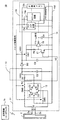
図1は、第1の実施の形態の無線タグの一例を示す図である。
Hereinafter, embodiments for carrying out the invention will be described with reference to the drawings.
(First embodiment)
FIG. 1 is a diagram illustrating an example of a wireless tag according to the first embodiment.
無線タグ1aは、送受信機(以下リーダライタと呼ぶ)1bが送信する電磁波(搬送波)を受け、その電磁波に基づき電力を発生して動作するパッシブタイプのタグである。無線タグ1aは、アンテナ(コイル)2と、アンテナ2を介してリーダライタ1bと無線通信を行う無線通信回路3を有する。
The wireless tag 1a is a passive type tag that receives an electromagnetic wave (carrier wave) transmitted by a transceiver (hereinafter referred to as a reader / writer) 1b and operates by generating electric power based on the electromagnetic wave. The wireless tag 1 a includes an antenna (coil) 2 and a wireless communication circuit 3 that performs wireless communication with the reader /
アンテナ2は、接続部2a,2bで、無線通信回路3と接続されている。
無線通信回路3は、例えば、ICチップであり、リーダライタ1bから送信される電磁波により電源がオンされる。無線通信回路3は、キャパシタC0、スイッチSW1,SW2,SW3、整流回路4、回路部5、モニタ回路6、メイン回路7を有する。
The
The wireless communication circuit 3 is, for example, an IC chip, and the power is turned on by an electromagnetic wave transmitted from the reader /
キャパシタC0は、接続部2a,2bの間に接続されている。このキャパシタC0とアンテナ2とにより、並列共振回路が実現される。アンテナ2が、リーダライタ1bが送信する電磁波を受信したとき、電磁波により誘導される交流信号が、スイッチSW1,SW2を介して無線通信回路3の整流回路4に供給される。
The capacitor C0 is connected between the
スイッチSW1〜SW3は、メイン回路7によって制御される回路である。
スイッチSW1は、接続部2aを、整流回路4または抵抗R0の何れかに接続させる。リーダライタ1bと無線通信回路3との間で無線通信が行われているとき(以下通常動作時という)ではスイッチSW1により、接続部2aと整流回路4とが接続される。無線タグ1aの劣化を検出するための測定が行われるとき(以下モニタ動作時という)ではスイッチSW1により、接続部2aと抵抗R0とが接続される。
The switches SW1 to SW3 are circuits controlled by the main circuit 7.
The switch SW1 connects the
なお、モニタ動作は、リーダライタ1bによる電磁波の送信が停止され、電源電圧が無線タグ1aの通常動作電圧範囲から外れたときのタイミング、すなわち、無線通信回路3の電源がオフになったタイミングで行われる。
The monitoring operation is performed when the transmission of the electromagnetic wave by the reader /
スイッチSW2は、接続部2bを、整流回路4またはスイッチSW3の何れかに接続させる。スイッチSW2により、通常動作時では、接続部2bと整流回路4とが接続され、モニタ動作時では接続部2bとスイッチSW3とが接続される。
The switch SW2 connects the
スイッチSW3は、スイッチSW2と電源線VSS(例えば、接地電位となっている)との間に接続されている。スイッチSW3により、通常動作時にはスイッチSW2と電源線VSSとの間の接続が遮断され、モニタ動作時にはスイッチSW2と電源線VSSとが接続される。 The switch SW3 is connected between the switch SW2 and a power supply line VSS (for example, a ground potential). The switch SW3 cuts off the connection between the switch SW2 and the power supply line VSS during normal operation, and connects the switch SW2 and the power supply line VSS during monitoring operation.
整流回路4は、例えば、ダイオードブリッジを用いた全波整流回路などであり、アンテナ2から出力される交流信号を整流して、整流信号を生成する。また、生成された整流信号は、回路部5のキャパシタC1により平滑化され、メイン回路7に出力される。
The
回路部5は、リーダライタ1bから送信される電磁波を受信することにより電力が発生し電源電圧が無線タグ1aの通常動作電圧範囲に達しているとき、すなわち、無線通信回路3の電源がオンになっているときに、電荷を充電するキャパシタC1を含む。また、回路部5は、キャパシタC1に充電した電荷に基づく放電電流を、電源オフ時にアンテナ2を含む電流パスに流す。
The circuit unit 5 generates power by receiving the electromagnetic wave transmitted from the reader /
キャパシタC1は、電源線VDDと電源線VSSとの間に接続されている。また、キャパシタC1は、整流回路4から出力される整流信号を平滑化する機能も有する。
回路部5は、さらに、抵抗R0とスイッチSW4を有している。
The capacitor C1 is connected between the power supply line VDD and the power supply line VSS. The capacitor C1 also has a function of smoothing the rectified signal output from the
The circuit unit 5 further includes a resistor R0 and a switch SW4.
抵抗R0は、スイッチSW4とスイッチSW1との間に接続されている。
スイッチSW4は、一端が電源線VDDとキャパシタC1の一方の端子の間に接続され、他端が抵抗R0及びモニタ回路6に接続されている。スイッチSW4は、通常動作時にはオフし、モニタ動作時にはオンする回路である。
The resistor R0 is connected between the switch SW4 and the switch SW1.
The switch SW4 has one end connected between the power supply line VDD and one terminal of the capacitor C1, and the other end connected to the resistor R0 and the
電源オン時の通常動作時にスイッチSW4がオフすることで、整流回路4から出力される整流信号によりキャパシタC1に電荷が充電される。また、電源オフ時のモニタ動作時にSW4がオンすることで、キャパシタC1に充電された電荷は、モニタ回路6に供給され、また、抵抗R0を介してアンテナ2を含む電流パスに放電される。
When the switch SW4 is turned off during the normal operation when the power is turned on, the capacitor C1 is charged with the rectified signal output from the
放電電流が流れる電流パスについて以下説明する。
電源オフ時のモニタ動作時では、上記のように、スイッチSW4がオンしキャパシタC1と抵抗R0とが接続され、また、スイッチSW1により抵抗R0と接続部2aとが接続される。さらに、スイッチSW2により接続部2bとスイッチSW3とが接続され、また、スイッチSW3がオンすることにより、接続部2bが、スイッチSW2,SW3を介して電源線VSSに接続される。これにより、キャパシタC1の電源線VDDに接続されている端子から、抵抗R0、接続部2a、アンテナ2、接続部2bを介して、電源線VSSに至る電流パスが形成される。
The current path through which the discharge current flows will be described below.
During the monitoring operation when the power is turned off, the switch SW4 is turned on to connect the capacitor C1 and the resistor R0 as described above, and the resistor R0 and the
さらに、上記の電流パスにおいて、アンテナ2などを抵抗としてみると、電源線VDDと電源線VSSとの間に直列に接続された、抵抗R0、接続部2a、アンテナ2、接続部2bを含む抵抗分圧回路が形成されている。そのため、抵抗R0と接続部2a間のノードN1の電位V1は、電源線VDDの電圧を、電流パスにおいてキャパシタC1からノードN1までの合成抵抗と、電流パスのその他の部分(アンテナ2を含む部分)の合計抵抗値との比により分圧した値となる。これにより、例えば、アンテナ2自体の劣化や接続部2a,2bの劣化が生じると、接続部2a,2b、アンテナ2の合計抵抗値が高くなるため、電位V1は高くなる。
Further, in the above current path, when the
なお、抵抗R0の抵抗値は、アンテナ2が正常である場合、電位V1が、以下で説明するモニタ回路6の閾値Vthを超えないように調整されている。
モニタ回路6は、電源オフ時に、キャパシタC1に充電されている電荷に基づく電力によって動作し、上記電流パスのノードN1の電位V1に基づき劣化の有無を判定する。
The resistance value of the resistor R0 is adjusted so that the potential V1 does not exceed the threshold value Vth of the
The
例えば、モニタ回路6は、モニタ動作時、電位V1を所定の閾値Vthと比較して、電位V1が閾値Vthを上回っている場合、劣化が生じていると判定し、検出結果としてメイン回路7に供給するアラーム信号をLowレベルからHighレベルに上げる。
For example, during the monitoring operation, the
メイン回路7は、モニタ回路6での判定結果を記憶する記憶回路部8を有している。例えば、記憶回路部8は、アラーム信号がHighレベルのときは、“1”を記憶し、アラーム信号がLowレベルのときは、“0”を記憶する。
The main circuit 7 includes a storage circuit unit 8 that stores the determination result in the
なお、メイン回路7は、図示しないアナログ回路などを有し、通常動作時には、変調処理や復調処理を行う。例えば、メイン回路7は、リーダライタ1bから電磁波で送られてくるリード命令に応じて記憶回路部8に記憶されているデータを読み出して変調して、整流回路4を介してアンテナ2に出力する処理などを行う。
The main circuit 7 includes an analog circuit (not shown) and the like, and performs modulation processing and demodulation processing during normal operation. For example, the main circuit 7 reads and modulates the data stored in the storage circuit unit 8 in response to a read command sent as an electromagnetic wave from the reader /
なお、以下の説明では、モニタ回路6の動作や、記憶回路部8への書き込み動作は、通常動作電圧範囲よりも低い電圧範囲で実行可能であるものとする。
以下、第1の実施の形態の無線タグ1aの動作の一例を説明する。
In the following description, it is assumed that the operation of the
Hereinafter, an example of the operation of the wireless tag 1a according to the first embodiment will be described.
(無線タグの動作例)
図1の下側には、第1の実施の形態の無線タグの一例の動作を示すタイミングチャートが示され、また、電源線VDDの電圧(電源電圧)、電位V1、アラーム信号の一例の様子が示されている。
(Example of wireless tag operation)
A timing chart showing an example of the operation of the wireless tag according to the first embodiment is shown on the lower side of FIG. 1, and an example of the voltage (power supply voltage) of the power supply line VDD, the potential V1, and an alarm signal is shown. It is shown.
アンテナ2が、リーダライタ1bから送信される電磁波の受信を開始すると、電力が生じ徐々に電源電圧が上昇する。
タイミングt0で、電源電圧は無線タグ1aの動作電圧範囲に達している。これにより、無線タグ1aは、電源オン状態になる。さらに、このとき、スイッチSW4はオフ状態であるため、回路部5のキャパシタC1には、整流回路4から出力される整流信号により、電荷が充電される。
When the
At timing t0, the power supply voltage reaches the operating voltage range of the wireless tag 1a. As a result, the wireless tag 1a is turned on. Further, at this time, since the switch SW4 is in an off state, the capacitor C1 of the circuit unit 5 is charged with a charge by the rectification signal output from the
その後、リーダライタ1bが電磁波の供給を停止すると、徐々に電源電圧が降下する。
タイミングt1で、電源電圧は無線タグ1aの動作電圧範囲以下になる。これにより、無線タグ1aは、電源オフ状態(通常動作が停止されている状態)になる。ただ、このときメイン回路7によってスイッチSW1〜SW4が前述したような状態になり、キャパシタC1に充電された電荷に基づく放電電流が流れる電流パスが形成される。また、モニタ回路6は、キャパシタC1から供給される電力によって動作する。
Thereafter, when the reader /
At timing t1, the power supply voltage falls below the operating voltage range of the wireless tag 1a. As a result, the wireless tag 1a enters a power-off state (a state in which normal operation is stopped). However, at this time, the switches SW1 to SW4 are in the state as described above by the main circuit 7, and a current path through which a discharge current based on the charge charged in the capacitor C1 flows is formed. Further, the
図1の例では、タイミングt1で、電位V1が、モニタ回路6の閾値Vthを超えている。これにより、モニタ回路6が出力するアラーム信号がLowレベルからHighレベルに立ち上がり、メイン回路7の記憶回路部8は、例えば、劣化が生じた旨を示す“1”を記憶する。
In the example of FIG. 1, the potential V1 exceeds the threshold value Vth of the
なお、リーダライタ1bは、記憶回路部8に記憶された値を、次に無線タグ1aの電源をオンしたときに、読み出す。アンテナ2の劣化を簡単に判定することができる。
以上のような無線タグ1aでは、電源オン時に充電した電荷を利用して、電源オフのタイミングでアンテナ2を含む電流パスに流して、電流パスのノードN1の電位V1から劣化の有無を判定することで、劣化が無線タグ1a自身で自己診断できるようになる。そのため、無線タグ1aの劣化を測定するために、リーダライタの他に、無線タグ1aからの返信強度を測定する測定器などを用意したり、電磁波の影響の少ない環境を整えたりしなくてもよくなる。つまり、無線タグ1aの評価環境の準備が簡素化され、無線タグ1aの劣化検出が容易になる。
The reader /
In the wireless tag 1a as described above, the charge charged when the power is turned on is used to flow through the current path including the
さらに、無線タグ1aは、電源オフ時のキャパシタC1の残留電荷を利用して、アンテナ2の劣化を検出している。そのため、アンテナ2の劣化検出により、無線タグ1aのスタンバイ時や通常動作時の消費電流が増加することはない。また、無線タグ1aは、電源オフ時に、アンテナ2の劣化を検出しているので、無線タグ1aの通常動作に影響を及ぼさない。
Further, the wireless tag 1a detects the deterioration of the
また、リーダライタ1bが、無線タグ1aの電源オフ時に記憶回路部8に記憶された劣化検出結果を、次に無線タグ1aを使用する際に読み出すことで、アンテナ2が劣化しているか否かを判定できる。これにより、無線タグ1aの使用のたびに、アンテナ2が劣化しているか否かが判定されるので、アンテナ2が完全に壊れる前の劣化の段階での検出が可能となる。
Whether the
このような無線タグ1aは、高い信頼性が求められる用途に対し好適な無線タグである。例えば、図書館の蔵書管理では、十年以上に渡って管理が行われるものであるため、無線タグが劣化する可能性があるが、上記の無線タグ1aによれば、無線タグ1aが使用不能になる前に劣化を検出でき、トラブルの発生を抑制できる。 Such a wireless tag 1a is a wireless tag suitable for applications that require high reliability. For example, in library collection management, since the management is performed for more than a decade, the wireless tag may be deteriorated. However, according to the wireless tag 1a, the wireless tag 1a cannot be used. Deterioration can be detected before it occurs, and trouble can be suppressed.
(第2の実施の形態)
図2、図3は、第2の実施の形態の無線タグの一例を示す図である。なお、図2では、通常動作時の無線タグ10の状態が示されており、図3では、モニタ動作時の無線タグ10の状態が示されている。
(Second Embodiment)
2 and 3 are diagrams illustrating an example of a wireless tag according to the second embodiment. FIG. 2 shows the state of the
なお、第1の実施の形態の無線タグ1aと同様の要素については、同一符号を付し、その説明を一部省略する。
無線タグ10は、パッシブタイプのタグであり、アンテナ2と、アンテナ2を介してリーダライタ1bと無線通信を行い、リーダライタ1bから送信される電磁波により電源がオンされる無線通信回路11を有する。
In addition, about the element similar to the wireless tag 1a of 1st Embodiment, the same code | symbol is attached | subjected and the description is partially omitted.
The
無線通信回路11は、例えば、ICチップであり、キャパシタC0、スイッチSW5,SW6,SW7、整流回路12、回路部13、モニタ回路14、メイン回路15、ダイオードD0、キャパシタC3を有する。
The
スイッチSW5〜SW7は、メイン回路7によって制御される回路である。
スイッチSW5は、接続部2bと、電源線VSSとの間に接続されている。スイッチSW5は、モニタ動作時にはオンし、図3に示すように、接続部2bと電源線VSSとを接続する。
The switches SW5 to SW7 are circuits controlled by the main circuit 7.
The switch SW5 is connected between the
スイッチSW6は、接続部2aと、後述する回路部13の抵抗R1との間に接続されている。スイッチSW6は、モニタ動作時にはオンし、図3に示すように接続部2aと抵抗R1とを接続する。
The switch SW6 is connected between the
なお、スイッチSW5,SW6は、後述の回路部13とともに、第1の実施の形態の無線通信回路3における回路部5の機能を実現する。
スイッチSW7は、キャパシタC3と電源線VDD1の間に一端が接続されており、他端がモニタ回路14に接続されている。スイッチSW7は、モニタ動作時にはオンし、図3に示すように、電源線VDD1、キャパシタC3及びモニタ回路14を接続する。
Note that the switches SW5 and SW6 together with the
The switch SW7 has one end connected between the capacitor C3 and the power supply line VDD1, and the other end connected to the
整流回路12は、ダイオードブリッジによる全波整流回路であり、ブリッジ状に接続されたダイオードD1,D2,D3,D4を有している。ダイオードD1のカソードとダイオードD2のアノードは、接続部2aとスイッチSW6に接続され、ダイオードD3のカソードとダイオードD4のアノードは、接続部2bとスイッチSW5に接続されている。また、ダイオードD1,D3のアノードは、スイッチSW5及び電源線VSSに接続され、ダイオードD2,D4のカソードは、抵抗R1とキャパシタC2の一方の端子(電源線VDD2に接続されている側)及びダイオードD0のアノードに接続されている。
The
整流回路12は、アンテナ2から出力される交流信号を全波整流して整流信号を生成する。また、生成された整流信号は、回路部13のキャパシタC2とキャパシタC3により平滑化され、メイン回路7に出力される。
The
回路部13は、抵抗R1とキャパシタC2を有する。
抵抗R1は、スイッチSW6と、キャパシタC2の一方の端子(電源線VDD2に接続されている側)と、ダイオードD0との間に接続されている。
The
The resistor R1 is connected between the switch SW6, one terminal of the capacitor C2 (side connected to the power supply line VDD2), and the diode D0.
キャパシタC2は、電源線VDD2と、電源線VSSとの間に接続されている。
通常動作時では、図2に示されているように、スイッチSW6がオフするため、整流回路12から出力される整流信号により、キャパシタC2に電荷が充電される。また、モニタ動作時では、図3に示されているように、SW6がオンするため、キャパシタC2に充電された電荷は、抵抗R1を介してアンテナ2を含む電流パスに放電される。以下、キャパシタC2の電荷が放電される電流パスについて説明する。
The capacitor C2 is connected between the power supply line VDD2 and the power supply line VSS.
During normal operation, as shown in FIG. 2, the switch SW6 is turned off, so that the capacitor C2 is charged by the rectified signal output from the
図3に示すモニタ動作時では、上記のように、スイッチSW6がオンし抵抗R1と接続部2aが接続し、また、スイッチSW5がオンし接続部2bと電源線VSSが接続する。すなわち、キャパシタC2の電源線VDD2に接続されている端子から、抵抗R1、接続部2b、アンテナ2、接続部2bを介して、電源線VSSに至る電流パスが形成される。
In the monitoring operation shown in FIG. 3, as described above, the switch SW6 is turned on to connect the resistor R1 and the connecting
さらに、上記の電流パスにおいて、アンテナなどを抵抗としてみると、電源線VDD2と電源線VSSとの間に直列に接続された、抵抗R1、接続部2a、アンテナ2、接続部2bを含む抵抗分圧回路が形成されている。
Further, in the above current path, when the antenna or the like is regarded as a resistor, the resistance component including the resistor R1, the
抵抗R1を、電流パスにおける無線通信回路11内の抵抗と考えると、抵抗R1と接続部2a間のノードN2の電位V2は、電源線VDD2の電圧を、接続部2a、アンテナ2、接続部2bの合計抵抗値と、抵抗R1の抵抗値の比により分圧した値となる。
Assuming that the resistor R1 is a resistor in the
例えば、アンテナ2自体の劣化や接続部2a,2bの劣化が生じると、上記の合計抵抗値が高くなるため、電位V2も高くなる。
なお、抵抗R1の抵抗値は、アンテナ2が正常な場合、電位V2が、後述するモニタ回路14のトランジスタ17の閾値Vthを超えないように調整されている。
For example, if the
Note that the resistance value of the resistor R1 is adjusted so that the potential V2 does not exceed a threshold value Vth of a
ダイオードD0は、アノードをキャパシタC2の電源線VDD2に接続された端子に接続し、カソードを、後述するキャパシタC3の電源線VDD1に接続された端子に接続している。ダイオードD0は、電源オフ時にキャパシタC3に充電された電荷が、キャパシタC2へ流出することを抑制する。 The diode D0 has an anode connected to a terminal connected to the power supply line VDD2 of the capacitor C2, and a cathode connected to a terminal connected to a power supply line VDD1 of the capacitor C3 described later. The diode D0 suppresses the charge charged in the capacitor C3 when the power is turned off from flowing out to the capacitor C2.
図3に示すモニタ動作時では、キャパシタC2の電荷は、上記のように電流パスを介して放電され、また、キャパシタC3の電荷は、後述するように、モニタ回路14とメイン回路15に供給される。そのため、放電されるキャパシタC2の電荷が、キャパシタC3の電荷より早く消費されてしまい、電源線VDD2の電位が電源線VDD1の電位より低くなる場合がある。このような場合、キャパシタC3の電荷が、キャパシタC2側に流れ出さないように、このようなダイオードD0が接続されている。
In the monitoring operation shown in FIG. 3, the charge of the capacitor C2 is discharged through the current path as described above, and the charge of the capacitor C3 is supplied to the
キャパシタC3は、電源線VDD1と電源線VSSとの間に接続されている。
通常動作時では、図2に示すように、スイッチSW7がオフするため、整流回路12から出力される整流信号により、キャパシタC3に電荷が充電される。また、モニタ動作時では、図3に示すように、スイッチSW7がオンするため、キャパシタC3の電荷は、モニタ回路14とメイン回路15に供給される。
The capacitor C3 is connected between the power supply line VDD1 and the power supply line VSS.
During normal operation, as shown in FIG. 2, the switch SW7 is turned off, so that the capacitor C3 is charged by the rectified signal output from the
モニタ回路14は、上記の電流パスのノードN2の電位V2に基づき劣化の有無を判定する。そして、判定結果をアラーム信号としてメイン回路15に通知する。
モニタ回路14は、nチャネル型トランジスタであるトランジスタ17、抵抗R2、インバータ回路18、キャパシタC4を有する。
The
The
トランジスタ17のゲートは、ノードN2に接続され、トランジスタ17の一方の入出力端子(ソース)は、電源線VSSに接続されている。また、トランジスタ17の他方の入出力端子(ドレイン)は、抵抗R2及びインバータ回路18の入力端子に接続されている。
The gate of the
抵抗R2は、スイッチSW7と、トランジスタ17の入出力端子(ドレイン)との間に接続されている。
インバータ回路18の入力端子は、抵抗R2とトランジスタ17の入出力端子(ドレイン)との間に接続され、インバータ回路18の出力端子は、メイン回路15のロジック回路15bに接続されている。また、インバータ回路18の電力供給端子は、スイッチSW7に接続され、インバータ回路18の接地端子は、電源線VSSに接続されている。
The resistor R2 is connected between the switch SW7 and the input / output terminal (drain) of the
The input terminal of the
キャパシタC4は、インバータ回路18の出力端子と、電源線VSSとの間に接続されている。
モニタ動作時、図3に示すように、スイッチSW7がオンするため、キャパシタC3の電荷は、インバータ回路18の電力供給端子に供給され、また、抵抗R2を介して、トランジスタ17の入出力端子(ドレイン)に供給される。さらに、トランジスタ17のゲートは、電位V2となる。
The capacitor C4 is connected between the output terminal of the
During the monitoring operation, as shown in FIG. 3, since the switch SW7 is turned on, the charge of the capacitor C3 is supplied to the power supply terminal of the
アンテナ2や接続部2a,2bが劣化している場合、前述のように、電位V2は高くなる。そして、電位V2がトランジスタ17の閾値Vthを上回ると、トランジスタ17はオン状態となり、トランジスタ17の入出力端子(ドレイン)にキャパシタC3から供給された電荷は、トランジスタ17の入出力端子(ソース)に放電される。これにより、トランジスタ17の入出力端子(ドレイン)すなわちインバータ回路18の入力端子の電位が下がる。さらに、インバータ回路18の入力端子の電位が、インバータ回路18の反転閾値に達すると、インバータ回路18は、論理レベルがHighレベルとなるアラーム信号を、メイン回路15に出力する。
When the
一方、アンテナ2や接続部2a,2bの劣化が生じていない場合、前述のように、電位V2はトランジスタ17の閾値Vthに達せず、トランジスタ17はオンしない。そのため、トランジスタ17の入出力端子(ドレイン)すなわちインバータ回路18の入力端子の電位は、キャパシタC3からの電荷の供給により高いままである。これにより、インバータ回路18から出力されるアラーム信号は、Lowレベルとなる。
On the other hand, when the
メイン回路15は、アナログ回路15a、ロジック回路15b、不揮発メモリ15cを有する。
アナログ回路15aは、電源線VDD1と、電源線VSSとの間に接続されている。アナログ回路15aは、不揮発メモリ15cから読み出したデータを、アンテナ2を介してリーダライタ1bに送信するための変調や、受信したデータの復調などの処理を行う制御回路である。また、アナログ回路15aは、ロジック回路15bと接続され、ロジック回路15bとの間で信号の送受信を行う。また、アナログ回路15aは、不揮発メモリ15cと接続され、メモリ制御信号を出力して不揮発メモリ15cを制御する。
The
The
電源オフ時、アナログ回路15aは、キャパシタC3から供給される電力により動作する。また、アナログ回路15aは、電源オフ時に電源線VDD1の電位が下降すると、モニタ動作を実行するために、スイッチ制御信号でスイッチSW5〜SW7をオンさせる。
When the power is off, the
ロジック回路15bも、電源線VDD1と、電源線VSSとの間に接続されている。ロジック回路15bは、アナログ回路15aから供給されるデジタル信号などの論理処理を行う制御回路である。また、ロジック回路15bは、不揮発メモリ15cに、データ、アドレス信号、ライト信号などを出力する。
The
電源オフ時、ロジック回路15bは、キャパシタC3から供給される電力により動作する。ロジック回路15bは、例えば、スイッチ制御信号を受け、このスイッチ制御信号がスイッチSW5〜SW7をオンするタイミングで、モニタ回路14での検出結果を書き込むアドレスの指定や、ライト信号の供給などを不揮発メモリ15cに対して行う。そして、ロジック回路15bは、モニタ回路14から供給されるアラーム信号の値に基づき、例えば、“1”または“0”を不揮発メモリ15cに、検出結果として書き込む。
When the power is off, the
不揮発メモリ15cも、電源線VDD1と、電源線VSSとの間に接続されている。不揮発メモリ15cは、無線タグ10で使用されるデータや、上記の劣化の検出結果などを記憶する。不揮発メモリ15cは、FeRAM(Ferroelectric Random Access Memory)やフラッシュメモリなどを用いることができる。
The
電源オフ時、不揮発メモリ15cは、キャパシタC3から供給される電力により動作し、アラーム信号に応じた値(例えば、“0”または“1”)を劣化有無の判定値として記憶する。
When the power is off, the
以下、第2の実施の形態の無線タグ10の動作の一例を説明する。まず、アンテナ2が劣化していない状態、すなわち、アンテナ2が正常な状態での無線タグ10の動作の一例を説明する。
Hereinafter, an example of the operation of the
(無線タグの動作例1)
図4は、アンテナなどが劣化していない状態での第2の実施の形態の無線タグの一例の動作を示すタイミングチャートである。
(Operation example 1 of wireless tag)
FIG. 4 is a timing chart showing an example of the operation of the wireless tag according to the second embodiment in a state where the antenna and the like are not deteriorated.
図4では、電源線VDD1,VDD2の電圧(電源電圧)、メモリ制御信号、スイッチ制御信号、スイッチSW5〜SW7、電位V2、アラーム信号の一例の様子が示されている。また、図4には、電源電圧において、無線タグ10の通常動作が行われる電圧範囲Vaと、電源オフ時のモニタ回路14及びメイン回路15の動作が行われる電圧範囲Vbが示されている。
FIG. 4 shows an example of voltages (power supply voltages) of the power supply lines VDD1 and VDD2, a memory control signal, a switch control signal, switches SW5 to SW7, a potential V2, and an alarm signal. FIG. 4 shows a voltage range Va in which the normal operation of the
アンテナ2が、リーダライタ1bから送信される電磁波の受信を開始すると、徐々に電源線VDD1,VDD2での電源電圧は上昇する。
タイミングt3で、電源線VDD1、VDD2での両電源電圧は、電圧範囲Vaに達している。これにより、無線タグ10は、通常動作が行われる電源オン状態になる。このとき、例えば、不揮発メモリ15cに書き込まれているデータが読み出され、アナログ回路15aにて変調され、整流回路12で整流され、アンテナ2を介してリーダライタ1bに送信される読み出し処理や、書き込み処理などが行われる。
When the
At timing t3, both power supply voltages on the power supply lines VDD1 and VDD2 reach the voltage range Va. As a result, the
さらに、このとき、スイッチSW5,SW6,SW7がオフ状態であるため、キャパシタC2,C3には、整流回路12から出力される整流信号により、電荷が充電される。
また、タイミングt3では、電源線VDD1での電源電圧が電圧範囲Vaに達することにより、アナログ回路15aから不揮発メモリ15cに供給されるメモリ制御信号が、LowレベルからHighレベルに立ち上がっている。
Further, at this time, since the switches SW5, SW6, and SW7 are in an off state, the capacitors C2 and C3 are charged with a rectification signal output from the
Further, at timing t3, the power supply voltage on the power supply line VDD1 reaches the voltage range Va, so that the memory control signal supplied from the
その後、リーダライタ1bが電磁波の供給を停止すると、徐々に電源線VDD1,VDD2での電源電圧が降下する。
タイミングt4で、電源線VDD1,VDD2での電源電圧は、電圧範囲Va以下になる。これにより、無線タグ10は、電源オフ状態(通常動作が停止されている状態)となり、キャパシタC3から供給される電力により、モニタ回路14、メイン回路15が動作するようになる。
Thereafter, when the reader /
At timing t4, the power supply voltage on the power supply lines VDD1 and VDD2 falls below the voltage range Va. As a result, the
電源線VDD1が電圧範囲Vbまで降下すると、アナログ回路15aは、スイッチ制御信号をLowレベルからHighレベルに立ち上げる。これにより、スイッチSW5〜SW7がオンする。スイッチSW5〜SW7がオン状態となることで、キャパシタC2に充電された電荷が、抵抗R1、接続部2a、アンテナ2、接続部2bを介して、電源線VSSへ放電される。
When the power supply line VDD1 falls to the voltage range Vb, the
また、タイミングt4で、電位V2が0Vから立ち上がっているが、アンテナ2などが劣化していない状態である場合、モニタ回路14のトランジスタ17の閾値Vthに達しない。そのため、ロジック回路15bは、アラーム信号をLowレベルに維持する。これにより、不揮発メモリ15cには、例えば、“0”が記憶される。
Further, when the potential V2 rises from 0V at the timing t4, but the
タイミングt5で、電源線VDD1が電圧範囲Vb以下になる。これにより、アナログ回路15aが出力するスイッチ制御信号がLowレベルに立ち下がり、スイッチSW5〜SW7がオフする。スイッチSW5〜SW7がオフ状態となることで、キャパシタC3から電力が供給されなくなるため、モニタ回路14、メイン回路15は動作を停止する。
At timing t5, the power supply line VDD1 falls below the voltage range Vb. As a result, the switch control signal output from the
次に、アンテナ2などが劣化している状態での、無線タグ10の動作の一例を説明する。
(無線タグの動作例2)
図5は、アンテナなどが劣化している状態での第2の実施の形態の無線タグの一例の動作を示すタイミングチャートである。
Next, an example of the operation of the
(Operation example 2 of wireless tag)
FIG. 5 is a timing chart illustrating an example of the operation of the wireless tag according to the second embodiment in a state where the antenna or the like is deteriorated.
図5では、図4に示したものと同じ信号や電圧などについての、アンテナなどが劣化している状態での様子が示されている。
タイミングt6での動作は、図4に示したタイミングt3での動作と同じである。
FIG. 5 shows a state in which the antenna and the like are deteriorated with respect to the same signals and voltages as those shown in FIG.
The operation at timing t6 is the same as the operation at timing t3 shown in FIG.
タイミングt7において、アンテナ2や接続部2a,2bが劣化している場合では、劣化していない場合よりも電位V2は高くなる。図5の例では、電位V2は、モニタ回路14のトランジスタ17の閾値Vthを超えている。これにより、モニタ回路14のインバータ回路18から出力されるアラーム信号はHighレベルとなる。これにより、不揮発メモリ15cには、例えば、“1”が記憶される。
At timing t7, when the
タイミングt8で、電位V2は、モニタ回路14のトランジスタ17の閾値Vth以下になる。これにより、アラーム信号は、HighレベルからLowレベルに立ち下がる。
タイミングt9の処理は、図4に示したタイミングt5の処理と同じである。
At timing t8, the potential V2 becomes equal to or lower than the threshold value Vth of the
The process at timing t9 is the same as the process at timing t5 shown in FIG.
リーダライタ1bは、不揮発メモリ15cに記憶された、劣化の有無を示す1ビットデータを、次に無線タグ10を使用する際の電源オン時(図4、図5の例ではタイミングt3,t6)に読み出すことで、アンテナ2の劣化の有無を検出することができる。例えば、リーダライタ1bは、読み出されたデータが、“0”であればアンテナ2は正常であり、“1”であればアンテナ2は劣化していると判定する。アンテナ2が劣化していると判定した場合には、リーダライタ1bは、例えば、表示装置に「アンテナ劣化発見、早めに取り替えてください」などと、警告を表示してもよい。
The reader /
以下、リーダライタ1bでの動作を含めた劣化検出方法の流れをフローチャートでまとめる。
図6は、劣化検出方法の一例の流れを示すフローチャートである。
Hereinafter, the flow of the deterioration detection method including the operation in the reader /
FIG. 6 is a flowchart showing a flow of an example of the deterioration detection method.
まず、リーダライタ1bは、電磁波を無線タグ10に送信し、無線タグ10の電源をオンする(ステップS1)。これにより無線タグ10での通常動作が開始される。また、電源がオンすると、無線タグ10のキャパシタC2,C3に電荷が充電される(ステップS2)。
First, the reader /
リーダライタ1bは、電磁波の送信を停止し、無線タグ10の電源をオフする(ステップS3)。これにより、無線タグ10での通常動作が終了する。
しかし、無線タグ10では、キャパシタC2,C3に充電されていた電荷に基づく電力により、前述した劣化判定が行われる(ステップS4)。
The reader /
However, in the
そして、劣化判定の結果が不揮発メモリ15cに記憶される(ステップS5)。
次に、リーダライタ1bにより、無線タグ10の電源がオンされ、通常動作が開始すると(ステップS6)、無線タグ10は、不揮発メモリ15cに記憶された判定結果のデータを読み出し、読み出された判定結果のデータをアンテナ2を介してリーダライタ1bに出力する(ステップS7)。
Then, the result of the deterioration determination is stored in the
Next, when the power of the
以上のような無線タグ10及びそれを用いた劣化検出方法では、第1の実施の形態の無線タグ1aと同様の効果が得られる。
さらに、無線タグ10では、2つのキャパシタC2,C3を有しており、通常動作時にキャパシタC2に充電された電荷は、電源オフ時、電流パスへ放電され、キャパシタC3に充電された電荷は、モニタ回路14及びメイン回路15への電力供給に用いられる。これにより、電流パスへの放電電流のピーク値を確保でき、また、モニタ回路14とメイン回路15の動作を安定させることができる。
In the
Further, the
(変形例)
図7は、第2の実施の形態の無線タグの変形例を示す図である。なお、図2に示した無線タグ10と同様の要素については、同一符号を付し、その説明を省略する。
(Modification)
FIG. 7 is a diagram illustrating a modification of the wireless tag according to the second embodiment. The same elements as those of the
無線タグ10aにおいて無線通信回路11aの整流回路12aは、図2、図3に示した無線通信回路11の整流回路12と異なり、キャパシタC5,C6、ダイオードD5,D6を備えた半波整流回路である。
In the
キャパシタC5の一方の端子は、接続部2a、キャパシタC0の一方の端子及びスイッチSW6の一端に接続されている。キャパシタC5の他方の端子は、ダイオードD5のカソード及びダイオードD6のアノードに接続されている。また、キャパシタC6の一方の端子は、ダイオードD6のカソード、抵抗R1及び電源線VDD2に接続され、他方の端子は、電源線VSSに接続されている。
One terminal of the capacitor C5 is connected to the
ダイオードD5のカソードは、キャパシタC5の他方の端子とダイオードD6のアノードとの間に接続されており、アノードは電源線VSSに接続されている。また、ダイオードD6のアノードは、キャパシタC5の他方の端子及びダイオードD5のカソードに接続されており、カソードは、キャパシタC6の一方の端子、抵抗R1、電源線VDD2に接続されている。 The cathode of the diode D5 is connected between the other terminal of the capacitor C5 and the anode of the diode D6, and the anode is connected to the power supply line VSS. The anode of the diode D6 is connected to the other terminal of the capacitor C5 and the cathode of the diode D5, and the cathode is connected to one terminal of the capacitor C6, the resistor R1, and the power supply line VDD2.
このような無線タグ10aであっても、無線タグ10と同様の効果が得られる。
以上、実施の形態に基づき、本発明の無線タグ、無線通信回路及び劣化検出方法の一観点について説明してきたが、これらは一例にすぎず、上記の記載に限定されるものではない。
Even with such a
As described above, one aspect of the wireless tag, the wireless communication circuit, and the deterioration detection method of the present invention has been described based on the embodiments. However, these are merely examples, and the present invention is not limited to the above description.
1a 無線タグ
1b 送受信機(リーダライタ)
2 アンテナ
2a,2b 接続部
3 無線通信回路
4 整流回路
5 回路部
6 モニタ回路
7 メイン回路
8 記憶回路部
C0,C1 キャパシタ
N1 ノード
R0 抵抗
SW1〜SW4 スイッチ
VDD,VSS 電源線
2
Claims (9)
前記アンテナを介して送受信機と無線通信を行い、前記送受信機から送信される電磁波により電源がオンされる無線通信回路と、を有し、
前記無線通信回路は、
電源オン時に電荷を充電するキャパシタを含み前記キャパシタに充電した前記電荷に基づく放電電流を、電源オフ時に前記アンテナを含む電流パスに流す回路部と、
前記電源オフ時に、前記電荷に基づく電力によって動作し、前記電流パスにおけるノードの電位に基づき劣化の有無を判定するモニタ回路と、
前記モニタ回路での判定結果を記憶する記憶回路部と、
を有することを特徴とする無線タグ。 An antenna,
A wireless communication circuit that performs wireless communication with a transceiver via the antenna and is turned on by electromagnetic waves transmitted from the transceiver;
The wireless communication circuit is
A circuit unit that includes a capacitor that charges a charge when the power is turned on, and a circuit that causes a discharge current based on the charge charged in the capacitor to flow through a current path that includes the antenna when the power is turned off;
A monitor circuit that operates with the electric power based on the electric charge when the power is turned off, and determines the presence or absence of deterioration based on the potential of the node in the current path;
A storage circuit unit for storing a determination result in the monitor circuit;
A wireless tag comprising:
前記アンテナと前記第1のキャパシタの間に設けられた第1のスイッチと、
前記モニタ回路と前記第2のキャパシタの間に設けられた第2のスイッチと、
前記電源オフ時に、前記第1の電荷に基づく前記放電電流が前記電流パスに流れるように、前記第1のスイッチをオンさせ、前記第2の電荷に基づく前記電力によって前記モニタ回路が動作するように、前記第2のスイッチをオンさせる制御回路を有することを特徴とする請求項2または3に記載の無線タグ。 The wireless communication circuit is
A first switch provided between the antenna and the first capacitor;
A second switch provided between the monitor circuit and the second capacitor;
When the power is turned off, the first switch is turned on so that the discharge current based on the first charge flows through the current path, and the monitor circuit is operated by the power based on the second charge. The wireless tag according to claim 2, further comprising a control circuit that turns on the second switch.
電源オン時に電荷を充電するキャパシタを含み前記キャパシタに充電した前記電荷に基づく放電電流を、電源オフ時に前記アンテナを含む電流パスに流す回路部と、
前記電源オフ時に、前記電荷に基づく電力によって動作し、前記電流パスにおけるノードの電位に基づき劣化の有無を判定するモニタ回路と、
前記モニタ回路での判定結果を記憶する記憶回路部と、
を有することを特徴とする無線通信回路。 A wireless communication circuit that performs wireless communication with a transceiver via an antenna and is turned on by electromagnetic waves transmitted from the transceiver,
A circuit unit that includes a capacitor that charges a charge when the power is turned on, and a circuit that causes a discharge current based on the charge charged in the capacitor to flow through a current path that includes the antenna when the power is turned off;
A monitor circuit that operates with the electric power based on the electric charge when the power is turned off, and determines the presence or absence of deterioration based on the potential of the node in the current path;
A storage circuit unit for storing a determination result in the monitor circuit;
A wireless communication circuit comprising:
前記モニタ回路と前記第2のキャパシタの間に設けられた第2のスイッチと、
前記電源オフ時に、前記第1の電荷に基づく前記放電電流が前記電流パスに流れるように、前記第1のスイッチをオンさせ、前記第2の電荷に基づく前記電力によって前記モニタ回路が動作するように、前記第2のスイッチをオンさせる制御回路と、を有することを特徴とする請求項6または7に記載の無線通信回路。 A first switch provided between the antenna and the first capacitor;
A second switch provided between the monitor circuit and the second capacitor;
When the power is turned off, the first switch is turned on so that the discharge current based on the first charge flows through the current path, and the monitor circuit is operated by the power based on the second charge. The wireless communication circuit according to claim 6, further comprising: a control circuit that turns on the second switch.
前記送受信機は、前記無線タグに電磁波を送信して前記無線タグの電源をオンし、
前記無線通信回路は、前記電源がオンのときに、キャパシタに電荷を充電し、
前記送受信機は、前記電磁波の送信を停止して前記電源をオフし、
前記無線通信回路は、前記キャパシタに充電した前記電荷に基づく放電電流を、前記電源がオフのときに、前記アンテナを含む電流パスに流し、前記電流パスにおけるノードの電位に基づき劣化の有無を判定し、
前記無線通信回路は、前記劣化の有無の判定結果を記憶回路部に記憶し、
前記無線通信回路は、前記送受信機が次に前記電源をオンしたときに、前記記憶回路部に記憶された前記判定結果を読み出し、前記読み出された判定結果を、前記アンテナを介して前記送受信機に出力する、
ことを特徴とする劣化検出方法。 A deterioration detection method for detecting deterioration of a wireless tag including an antenna and a wireless communication circuit that performs wireless communication with a transceiver via the antenna,
The transceiver transmits electromagnetic waves to the wireless tag to turn on the wireless tag,
The wireless communication circuit charges a capacitor when the power is on,
The transceiver stops transmitting the electromagnetic wave and turns off the power;
The wireless communication circuit causes a discharge current based on the charge charged in the capacitor to flow in a current path including the antenna when the power is off, and determines whether there is deterioration based on a potential of a node in the current path And
The wireless communication circuit stores a determination result of the presence or absence of the deterioration in a storage circuit unit,
The wireless communication circuit reads out the determination result stored in the storage circuit unit when the transceiver next turns on the power, and transmits and receives the read determination result via the antenna. Output to the machine,
A deterioration detection method characterized by the above.
Priority Applications (2)
| Application Number | Priority Date | Filing Date | Title |
|---|---|---|---|
| JP2014165755A JP6384193B2 (en) | 2014-08-18 | 2014-08-18 | Wireless tag, wireless communication circuit, and degradation detection method |
| US14/810,009 US9582745B2 (en) | 2014-08-18 | 2015-07-27 | Wireless tag, wireless communication circuit, and degradation detection method |
Applications Claiming Priority (1)
| Application Number | Priority Date | Filing Date | Title |
|---|---|---|---|
| JP2014165755A JP6384193B2 (en) | 2014-08-18 | 2014-08-18 | Wireless tag, wireless communication circuit, and degradation detection method |
Publications (2)
| Publication Number | Publication Date |
|---|---|
| JP2016042649A JP2016042649A (en) | 2016-03-31 |
| JP6384193B2 true JP6384193B2 (en) | 2018-09-05 |
Family
ID=55302394
Family Applications (1)
| Application Number | Title | Priority Date | Filing Date |
|---|---|---|---|
| JP2014165755A Active JP6384193B2 (en) | 2014-08-18 | 2014-08-18 | Wireless tag, wireless communication circuit, and degradation detection method |
Country Status (2)
| Country | Link |
|---|---|
| US (1) | US9582745B2 (en) |
| JP (1) | JP6384193B2 (en) |
Families Citing this family (4)
| Publication number | Priority date | Publication date | Assignee | Title |
|---|---|---|---|---|
| EP3465924B1 (en) | 2016-06-02 | 2020-10-21 | The North Face Apparel Corp. | Intelligent toe cap |
| CN107329621B (en) * | 2017-07-04 | 2019-07-26 | 京东方科技集团股份有限公司 | Touch panel and its driving method and touch device |
| US20200161889A1 (en) * | 2018-11-16 | 2020-05-21 | T-Mobile Usa, Inc. | Over-the-air wireless charging |
| JP7036172B2 (en) | 2020-09-04 | 2022-03-15 | 日本電気株式会社 | Management equipment, management method, program |
Family Cites Families (17)
| Publication number | Priority date | Publication date | Assignee | Title |
|---|---|---|---|---|
| US7035773B2 (en) | 2002-03-06 | 2006-04-25 | Fisher-Rosemount Systems, Inc. | Appendable system and devices for data acquisition, analysis and control |
| US7295119B2 (en) | 2003-01-22 | 2007-11-13 | Wireless Valley Communications, Inc. | System and method for indicating the presence or physical location of persons or devices in a site specific representation of a physical environment |
| JP2005030877A (en) | 2003-07-11 | 2005-02-03 | Hitachi Ltd | Semiconductor integrated circuit device equipped with radio control test function |
| JP4529421B2 (en) | 2003-11-20 | 2010-08-25 | 富士ゼロックス株式会社 | Wireless information processing apparatus, image forming apparatus, and wireless information processing apparatus self-diagnosis method |
| US7883019B2 (en) | 2005-09-02 | 2011-02-08 | Hynix Semiconductor Inc. | Integrated circuit with embedded FeRAM-based RFID |
| JP5192732B2 (en) * | 2006-05-31 | 2013-05-08 | 株式会社半導体エネルギー研究所 | Semiconductor device and IC label, IC tag, and IC card including the semiconductor device |
| JP2008011696A (en) | 2006-06-02 | 2008-01-17 | Semiconductor Energy Lab Co Ltd | Capacitor device and mobile electronic equipment provided with the same |
| US8132026B2 (en) | 2006-06-02 | 2012-03-06 | Semiconductor Energy Laboratory Co., Ltd. | Power storage device and mobile electronic device having the same |
| JP5133607B2 (en) * | 2007-06-05 | 2013-01-30 | トッパン・フォームズ株式会社 | RFID media |
| JP2009020856A (en) | 2007-07-10 | 2009-01-29 | Toshiba Tec Corp | Handy-type wireless tag reader/writer |
| US20090015408A1 (en) | 2007-07-10 | 2009-01-15 | Yoshinori Asai | Handy-type wireless tag reader/writer |
| US7612325B1 (en) * | 2007-08-22 | 2009-11-03 | Watkins Jr Kenneth S | Electrical sensor for monitoring degradation of products from environmental stressors |
| JP4823259B2 (en) | 2008-03-14 | 2011-11-24 | 日本電信電話株式会社 | Electronic circuit, wireless terminal and wireless terminal system |
| JP2009302736A (en) * | 2008-06-11 | 2009-12-24 | Mitsubishi Electric Corp | Antenna connection detection circuit |
| JP2010010841A (en) * | 2008-06-24 | 2010-01-14 | Toyota Motor Corp | Wireless communication device |
| JP5243189B2 (en) | 2008-10-31 | 2013-07-24 | 太平洋セメント株式会社 | Piezoelectric power generation module, wireless transmission system using the same, and wind speed monitoring system |
| JP5884344B2 (en) * | 2011-09-01 | 2016-03-15 | セイコーエプソン株式会社 | Circuit device, electronic device and IC card |
-
2014
- 2014-08-18 JP JP2014165755A patent/JP6384193B2/en active Active
-
2015
- 2015-07-27 US US14/810,009 patent/US9582745B2/en active Active
Also Published As
| Publication number | Publication date |
|---|---|
| US9582745B2 (en) | 2017-02-28 |
| US20160048711A1 (en) | 2016-02-18 |
| JP2016042649A (en) | 2016-03-31 |
Similar Documents
| Publication | Publication Date | Title |
|---|---|---|
| US7806332B2 (en) | Passive type RFID semiconductor device, IC tag, and control method | |
| US10554261B2 (en) | Card detection device having a magnetic field monitor, system including the device, and method of operating the device | |
| US9305193B2 (en) | Contactless communication device and user device including the same | |
| JP6384193B2 (en) | Wireless tag, wireless communication circuit, and degradation detection method | |
| US8138893B2 (en) | Semiconductor integrated circuit device | |
| US7583180B2 (en) | Semiconductor device for passive RFID, IC tag, and control method thereof | |
| US9082057B2 (en) | RF device with tamper detection | |
| JP2001504625A (en) | Minimum voltage radio frequency identification | |
| US20100277282A1 (en) | Radio frequency identification tag | |
| CN103210597A (en) | A transponder, RFID system and methods of operation | |
| JP2010092394A (en) | Semiconductor device and rfid tag chip | |
| JP2006504211A (en) | Current integrated sense amplifier for memory modules in RFID | |
| KR100662615B1 (en) | Apparatus for transforming of a signal and apparatus for rfid tag having the same and method of driving the rfid tag | |
| JP2009507285A (en) | Passive contactless integrated circuit with flag for monitoring erase / programming voltage | |
| US9530088B2 (en) | Radio frequency identification devices | |
| KR100874983B1 (en) | Tag chip and its driving method | |
| EP3862924A1 (en) | Agile time-continuous memory operation for a radio frequency identification transponder | |
| KR101031414B1 (en) | Rfid device | |
| KR101068308B1 (en) | RFID device | |
| KR101939239B1 (en) | Envelop Detector for RF Communication | |
| Zuriarrain et al. | A CMOS low frequency analog RFID front-end for the IoT | |
| KR101218280B1 (en) | RFID device | |
| JP2019219346A (en) | Capacitance sensor circuit, transmitter, receiver, and semiconductor integrated circuit | |
| JP2005222278A (en) | Inlet for non-contact ic medium, non-contact ic medium, and communication system using it | |
| KR101067876B1 (en) | Sensing device of RFID |
Legal Events
| Date | Code | Title | Description |
|---|---|---|---|
| A621 | Written request for application examination |
Free format text: JAPANESE INTERMEDIATE CODE: A621 Effective date: 20170712 |
|
| TRDD | Decision of grant or rejection written | ||
| A01 | Written decision to grant a patent or to grant a registration (utility model) |
Free format text: JAPANESE INTERMEDIATE CODE: A01 Effective date: 20180710 |
|
| A977 | Report on retrieval |
Free format text: JAPANESE INTERMEDIATE CODE: A971007 Effective date: 20180711 |
|
| A61 | First payment of annual fees (during grant procedure) |
Free format text: JAPANESE INTERMEDIATE CODE: A61 Effective date: 20180723 |
|
| R150 | Certificate of patent or registration of utility model |
Ref document number: 6384193 Country of ref document: JP Free format text: JAPANESE INTERMEDIATE CODE: R150 |