JP2009507285A - Passive contactless integrated circuit with flag for monitoring erase / programming voltage - Google Patents
Passive contactless integrated circuit with flag for monitoring erase / programming voltage Download PDFInfo
- Publication number
- JP2009507285A JP2009507285A JP2008528549A JP2008528549A JP2009507285A JP 2009507285 A JP2009507285 A JP 2009507285A JP 2008528549 A JP2008528549 A JP 2008528549A JP 2008528549 A JP2008528549 A JP 2008528549A JP 2009507285 A JP2009507285 A JP 2009507285A
- Authority
- JP
- Japan
- Prior art keywords
- high voltage
- memory
- vhv
- integrated circuit
- circuit
- Prior art date
- Legal status (The legal status is an assumption and is not a legal conclusion. Google has not performed a legal analysis and makes no representation as to the accuracy of the status listed.)
- Pending
Links
Images


Classifications
-
- G—PHYSICS
- G06—COMPUTING; CALCULATING OR COUNTING
- G06K—GRAPHICAL DATA READING; PRESENTATION OF DATA; RECORD CARRIERS; HANDLING RECORD CARRIERS
- G06K19/00—Record carriers for use with machines and with at least a part designed to carry digital markings
- G06K19/06—Record carriers for use with machines and with at least a part designed to carry digital markings characterised by the kind of the digital marking, e.g. shape, nature, code
- G06K19/067—Record carriers with conductive marks, printed circuits or semiconductor circuit elements, e.g. credit or identity cards also with resonating or responding marks without active components
- G06K19/07—Record carriers with conductive marks, printed circuits or semiconductor circuit elements, e.g. credit or identity cards also with resonating or responding marks without active components with integrated circuit chips
- G06K19/0723—Record carriers with conductive marks, printed circuits or semiconductor circuit elements, e.g. credit or identity cards also with resonating or responding marks without active components with integrated circuit chips the record carrier comprising an arrangement for non-contact communication, e.g. wireless communication circuits on transponder cards, non-contact smart cards or RFIDs
-
- G—PHYSICS
- G06—COMPUTING; CALCULATING OR COUNTING
- G06K—GRAPHICAL DATA READING; PRESENTATION OF DATA; RECORD CARRIERS; HANDLING RECORD CARRIERS
- G06K19/00—Record carriers for use with machines and with at least a part designed to carry digital markings
- G06K19/06—Record carriers for use with machines and with at least a part designed to carry digital markings characterised by the kind of the digital marking, e.g. shape, nature, code
- G06K19/067—Record carriers with conductive marks, printed circuits or semiconductor circuit elements, e.g. credit or identity cards also with resonating or responding marks without active components
- G06K19/07—Record carriers with conductive marks, printed circuits or semiconductor circuit elements, e.g. credit or identity cards also with resonating or responding marks without active components with integrated circuit chips
- G06K19/0701—Record carriers with conductive marks, printed circuits or semiconductor circuit elements, e.g. credit or identity cards also with resonating or responding marks without active components with integrated circuit chips at least one of the integrated circuit chips comprising an arrangement for power management
- G06K19/0713—Record carriers with conductive marks, printed circuits or semiconductor circuit elements, e.g. credit or identity cards also with resonating or responding marks without active components with integrated circuit chips at least one of the integrated circuit chips comprising an arrangement for power management the arrangement including a power charge pump
-
- G—PHYSICS
- G11—INFORMATION STORAGE
- G11C—STATIC STORES
- G11C16/00—Erasable programmable read-only memories
- G11C16/02—Erasable programmable read-only memories electrically programmable
- G11C16/06—Auxiliary circuits, e.g. for writing into memory
- G11C16/10—Programming or data input circuits
-
- G—PHYSICS
- G11—INFORMATION STORAGE
- G11C—STATIC STORES
- G11C5/00—Details of stores covered by group G11C11/00
- G11C5/14—Power supply arrangements, e.g. power down, chip selection or deselection, layout of wirings or power grids, or multiple supply levels
- G11C5/142—Contactless power supplies, e.g. RF, induction, or IR
-
- G—PHYSICS
- G11—INFORMATION STORAGE
- G11C—STATIC STORES
- G11C16/00—Erasable programmable read-only memories
- G11C16/02—Erasable programmable read-only memories electrically programmable
- G11C16/06—Auxiliary circuits, e.g. for writing into memory
- G11C16/30—Power supply circuits
Abstract
本発明は、電気的にプログラム可能な不揮発性データメモリ(MEM)と、前記メモリにデータ(DTW)を書き込むために必要な高電圧(Vhv)を供給するための電荷蓄積ブースタ回路(HVCT、PMP、HGEN)と備える受動型非接触式集積回路(IC2)に関するものである。本発明によれば、集積回路は、インジケータフラグ(THR2)を記憶するための揮発性の記憶手段(FF1)と、前記ブースタ回路を活性化した後で前記高電圧(Vhv)が最初に臨界しきい値(Vc)に到達するときに、前記インジケータフラグ(THR2)の値を変更するための手段(THDET、THR1、FF1)とを備える。 The present invention relates to an electrically programmable nonvolatile data memory (MEM) and a charge storage booster circuit (HVCT, PMP) for supplying a high voltage (Vhv) necessary for writing data (DTW) to the memory. , HGEN) and a passive non-contact integrated circuit (IC2). According to the present invention, in the integrated circuit, the volatile storage means (FF1) for storing the indicator flag (THR2) and the high voltage (Vhv) are first critical after the booster circuit is activated. And means (THDET, THR1, FF1) for changing the value of the indicator flag (THR2) when the threshold value (Vc) is reached.
Description
本発明は、データメモリと、メモリにデータを書き込むために必要な高電圧を供給するための電荷蓄積ブースタ回路とを備える非接触式集積回路に関係する。 The present invention relates to a contactless integrated circuit comprising a data memory and a charge storage booster circuit for supplying a high voltage necessary for writing data in the memory.
本発明は、更に特に、アンテナ信号から生成された電圧によって電気的に電力を供給される受動型の非接触式集積回路に関係する。 The present invention more particularly relates to a passive contactless integrated circuit that is electrically powered by a voltage generated from an antenna signal.
受動型非接触式集積回路は、一般的にRFIDアプリケーション(無線ICタグ)に使用されると共に、誘導結合タイプか、もしくは“電気的結合”タイプの集積回路であり得る。 Passive contactless integrated circuits are commonly used for RFID applications (wireless IC tags) and can be inductively coupled or “electrically coupled” type integrated circuits.
第1のタイプの受動型集積回路は、アンテナコイルと、負荷変調による送信データとを有すると共に、その周波数が通常約10[MHz]である磁界の存在下で誘導結合によって電力を供給される。これらの集積回路は、例えば13.56[MHz]の使用周波数を提供する標準“ISO/IEC 14443A/B”、“ISO/IEC 13693”によって説明される。 The first type of passive integrated circuit has an antenna coil and transmission data by load modulation, and is powered by inductive coupling in the presence of a magnetic field whose frequency is usually about 10 [MHz]. These integrated circuits are described by the standards “ISO / IEC 14443A / B”, “ISO / IEC 13693”, for example, which provide a working frequency of 13.56 [MHz].
第2のタイプの受動型集積回路は、数百MHzで振動するUHF電界によって電気的に電力を供給されると共に、それらのアンテナ回路の反射率を変調することによってデータを送信する(この技術は、後方散乱(backscattering)と呼ばれる)。これらの集積回路は、例えば標準化の途中の産業仕様書(industrial specification)EPCTM−GEN2(“Radio-Frequency Identity Protocols Class-1 Generation-2 - UHF RFID Protocol for Communications at 860 MHz-960 MHz”)によって説明される。それらは、一般的に、集積回路と、電界を放出する、データ送信/データ受信のためのステーション(装置)(一般に読み取り装置、リーダとも呼ばれる)との間の距離が、何メートルかに達し得る、長距離のアプリケーションに使用される。 A second type of passive integrated circuit is electrically powered by a UHF electric field that oscillates at several hundred MHz and transmits data by modulating the reflectivity of their antenna circuit (this technique is , Called backscattering). These integrated circuits are described, for example, by an industrial specification EPCTM-GEN2 ("Radio-Frequency Identity Protocols Class-1 Generation-2-UHF RFID Protocol for Communications at 860 MHz-960 MHz") in the process of standardization. Is done. They can generally reach several meters between an integrated circuit and a station (device) for data transmission / data reception (commonly called a reader, reader) that emits an electric field. Used for long distance applications.
図1は、第2のタイプの集積回路IC1の構造を概略的に示す。集積回路は、ダイポールアンテナ回路ACと、通信用インタフェース回路CICTと、制御ユニットCTU1と、EEPROM(電気的に消去可能であると共にプログラム可能であるメモリ)タイプの不揮発性メモリMEMと、電荷蓄積ブースタ回路HVCTと、そしてクロック信号CKをユニットCTU1に供給する発振器OSCとを備える。 FIG. 1 schematically shows the structure of a second type of integrated circuit IC1. The integrated circuit includes a dipole antenna circuit AC, a communication interface circuit CICT, a control unit CTU1, an EEPROM (electrically erasable and programmable memory) type nonvolatile memory MEM, and a charge storage booster circuit. HVCT and an oscillator OSC for supplying a clock signal CK to the unit CTU1.
回路CICTは、アンテナ回路を介したデータの受信及び送信を保証する。それは、制御ユニットCTU1から、アンテナ回路を介して送信されるべきデータDTxを受信するか、またはユニットCTU1に、アンテナ回路を介して受信されたデータDTrを供給する。更にそれは、集積回路の電源を保証すると共に、リーダ(読み取り装置)(図示せず)によって放出された電界Eの存在下で、アンテナ回路ACに記載されるアンテナ信号S1、S2から生成される電圧Vccを供給する。電圧Vccは、一般的に約1ボルトから数ボルトの範囲の電圧である。 The circuit CICT guarantees the reception and transmission of data via the antenna circuit. It receives data DTx to be transmitted via the antenna circuit from the control unit CTU1 or supplies the data DTr received via the antenna circuit to the unit CTU1. Furthermore, it guarantees the power supply of the integrated circuit and in the presence of an electric field E emitted by a reader (not shown), the voltage generated from the antenna signals S1, S2 described in the antenna circuit AC. Vcc is supplied. The voltage Vcc is generally in the range of about 1 volt to several volts.
ブースタ回路HVCTは、電圧Vccから、メモリにデータを書き込む動作に必要な一般的に約10〜15[V]の高電圧Vhvを供給する。電圧Vhvは、通常、ユニットCTU1によって制御されるスイッチ回路SCTを通じてメモリに印加される。 The booster circuit HVCT supplies, from the voltage Vcc, a high voltage Vhv that is generally about 10 to 15 [V] required for the operation of writing data into the memory. The voltage Vhv is normally applied to the memory through a switch circuit SCT controlled by the unit CTU1.
書き込み命令が受信されるとき、ユニットCTU1は、ブースタ回路HVCTを活性化し、書き込みアドレスADWと書き込まれるべきデータDTWをメモリMEMに印加し、そして電圧パルスVppがメモリに印加されるように、スイッチ回路SCTを活性化する。これらの動作は、ブースタ回路を活性化される状態にしている間に、実行されるべき書き込みサイクルの数に従って、数回繰り返され得る。 When a write command is received, the unit CTU1 activates the booster circuit HVCT, applies the write address ADW and the data DTW to be written to the memory MEM, and the switch circuit so that the voltage pulse Vpp is applied to the memory. Activates SCT. These operations can be repeated several times according to the number of write cycles to be performed while the booster circuit is activated.
集積回路の受動的性質に固有のこの集積回路の欠点は、そこから電源電圧Vccが抽出される電界Eの強度の変化によって引き起こされた臨界減衰(critical attenuation)を、電源電圧Vccが有し得るということである。磁界の強度、及び/またはリーダ(読み取り装置)との誘導結合の割合が不十分である場合、誘導結合タイプの受動型集積回路にも、類似する欠点がある。例えば、集積回路の利用者、例えば集積回路を含む非接触式チップカードの保持者が、リーダと集積回路との間の通信の間に、リーダからカード/集積回路を引き離すときに、これらの減衰は発生する。電源電圧のこれらの減衰は、それらがメモリにおけるデータの書き込みの間に発生するとき、それらが高電圧Vhvに影響を及ぼすことがあり得るので、解決が難しい。従って、集積回路がメモリの書き込みを始動させるとき、もし電圧Vhvが不十分なレベルを有している場合、メモリセルは、期待されたデータを格納しないか、またはメモリセルに格納されるデータの破損に対応して、プログラムされた状態でも消去された状態でもない中間の状態にセットされるであろう。 A disadvantage of this integrated circuit inherent to the passive nature of the integrated circuit is that the power supply voltage Vcc can have a critical attenuation caused by a change in the strength of the electric field E from which the power supply voltage Vcc is extracted. That's what it means. Inductive coupling type passive integrated circuits have similar disadvantages if the strength of the magnetic field and / or the rate of inductive coupling with the reader is insufficient. For example, when an integrated circuit user, such as a holder of a contactless chip card containing an integrated circuit, pulls the card / integrated circuit away from the reader during communication between the reader and the integrated circuit, these attenuations Will occur. These attenuations of the power supply voltage are difficult to solve because they can affect the high voltage Vhv when they occur during the writing of data in the memory. Thus, when the integrated circuit initiates a memory write, if the voltage Vhv has an insufficient level, the memory cell does not store the expected data or the data stored in the memory cell. In response to corruption, it will be set to an intermediate state that is neither programmed nor erased.
米国特許番号6288629号明細書は、データがメモリで書かれるときに電源電圧Vccを監視すると共に、電圧Vccが書き込み段階の間の臨界しきい値以下に変化するとき、インジケータフラグをたてることを提案する。書き込み段階が終了するとき、集積回路は、フラグを読み取ると共に、もし電圧Vccが書き込み段階の間に臨界しきい値未満になったことをそのフラグが示すならば、集積回路は、書き込み命令を発行したリーダに対して、この情報を通知する。 US Pat. No. 6,288,629 monitors power supply voltage Vcc when data is written in memory and sets an indicator flag when voltage Vcc changes below a critical threshold during the write phase. suggest. When the write phase is finished, the integrated circuit reads the flag and if the flag indicates that the voltage Vcc has fallen below the critical threshold during the write phase, the integrated circuit issues a write command. The reader is notified of this information.
具体的なアプリケーションに対応する動作条件における非接触式集積回路の動作の観測を目的とする様々なシミュレーションを含んでいる、本発明の著者によって実行された研究によると、この方法は、それが適切に発展したのに対して、書き込み動作が不完全であるという診断を導くことができる。実際には、様々な動作条件において、電源電圧Vccは、書き込みプロセスに影響を及ぼさない、減衰または本当に短いマイクロ切断を有し得ることが分かる。 According to studies performed by the authors of the present invention, including various simulations aimed at observing the operation of contactless integrated circuits at operating conditions corresponding to specific applications, this method is However, it can lead to a diagnosis that the writing operation is incomplete. In practice, it can be seen that, under various operating conditions, the power supply voltage Vcc can have an attenuation or a really short micro cut that does not affect the writing process.
従って、本発明は、適切に発展した書き込み動作が、電源電圧Vccがその変化の間に特定のしきい値を下回っていたということだけを根拠として、不完全であると見なされないように、不完全な書き込み動作の診断を改善することを目的とする。 Thus, the present invention is such that a properly developed write operation is not considered incomplete based solely on the fact that the power supply voltage Vcc was below a certain threshold during the change. It aims to improve the diagnosis of incomplete write operations.
本発明は、大部分の状況及び動作条件において、電荷がこの書き込み動作を達成することを可能にするようにブースタ回路が十分な電荷を蓄積したとき、書き込み動作が有効に実行され得るという記述に基づいている。本発明によれば、ブースタ回路によって供給された高電圧Vhvが“臨界”と呼ばれるしきい値に到達したときにこの条件は満たされる。従って、本発明によれば、電源電圧によって決まる代りに、ブースタ回路により供給された高電圧の値によって決まるインジケータフラグが提供される。このインジケータフラグは、書き込み動作を事後診断する(post-diagnose)ために使用され得るが、しかし、以下に現れることになるように、同様に様々な他の用途を有する。 The present invention describes that in most situations and operating conditions, a write operation can be performed effectively when the booster circuit has accumulated sufficient charge to allow the charge to achieve this write operation. Is based. According to the invention, this condition is satisfied when the high voltage Vhv supplied by the booster circuit reaches a threshold value called “critical”. Therefore, according to the present invention, instead of being determined by the power supply voltage, an indicator flag is provided that is determined by the value of the high voltage supplied by the booster circuit. This indicator flag can be used to post-diagnose write operations, but has various other uses as well, as will appear below.
更に特に、本発明は、電気的にプログラム可能な不揮発性データメモリと、前記メモリにデータを書き込むために必要な高電圧を供給するための電荷蓄積ブースタ回路と、前記インジケータフラグを記憶するための揮発性の記憶手段と、前記ブースタ回路を活性化した後で前記高電圧が最初に臨界しきい値に到達するときに、前記インジケータフラグの値を変更するための手段とを備える受動型非接触式集積回路を提供する。 More particularly, the present invention provides an electrically programmable non-volatile data memory, a charge storage booster circuit for supplying a high voltage required to write data to the memory, and a storage for the indicator flag. Passive non-contact comprising volatile storage means and means for changing the value of the indicator flag when the high voltage first reaches a critical threshold after activating the booster circuit An integrated circuit is provided.
一実施例によれば、集積回路は、前記メモリに前記高電圧を印加するためのスイッチ回路と、前記ブースタ回路を活性化した後で前記高電圧が前記臨界しきい値に到達しなかったならば、前記スイッチ回路が前記メモリに前記高電圧を印加することを回避するための手段とを備える。 According to one embodiment, the integrated circuit comprises: a switch circuit for applying the high voltage to the memory; and the high voltage does not reach the critical threshold after activating the booster circuit. For example, the switch circuit includes means for avoiding applying the high voltage to the memory.
一実施例によれば、前記スイッチ回路は、前記メモリに前記高電圧を徐々に供給するための傾斜波発生器を備える。 According to one embodiment, the switch circuit comprises a ramp generator for gradually supplying the high voltage to the memory.
一実施例によれば、集積回路は、前記メモリに前記データを書き込むための命令を実行するように構成されると共に、前記書き込むための命令の実行の間に前記高電圧が前記臨界しきい値に到達しなかったことを前記フラグが示すときに、その後特定の情報のメッセージを送信する制御ユニットを備える。 According to one embodiment, the integrated circuit is configured to execute an instruction to write the data to the memory, and the high voltage is set to the critical threshold during execution of the instruction to write. A control unit for transmitting a message of specific information after that when the flag indicates that it has not been reached.
一実施例によれば、集積回路は、前記メモリに前記データを書き込むための命令に応答して、以下の、前記ブースタ回路に、それが前記高電圧を生成するように、活性化信号を印加する動作と、前記メモリに書き込みアドレス及び書き込まれるべきデータを印加する動作と、前記メモリに対して前記高電圧を供給するスイッチ回路に活性化信号を印加する動作とを無条件に実行するように構成された制御ユニットを備える。 According to one embodiment, the integrated circuit applies an activation signal to the booster circuit, in response to an instruction to write the data to the memory, such that it generates the high voltage: An operation for applying a write address and data to be written to the memory, and an operation for applying an activation signal to the switch circuit for supplying the high voltage to the memory are unconditionally executed. A configured control unit is provided.
一実施例によれば、集積回路は、前記メモリに前記データを書き込むための命令を受信すると、以下の、前記ブースタ回路に、それが前記高電圧を生成するように、活性化信号を印加する動作と、前記メモリに書き込みアドレス及び書き込まれるべきデータを印加する動作と、もし前記高電圧が前記臨界しきい値に到達する場合、前記メモリに対して前記高電圧を供給するスイッチ回路に活性化信号を印加する動作と、もし前記高電圧が判定された期間の終りに前記臨界しきい値に到達しなかった場合、前記スイッチ回路に前記活性化信号を印加しないと共に、前記高電圧が前記メモリに印加されなかったことを示す特定の情報のメッセージを送信する動作とを実行するように構成された制御ユニットを備える。 According to one embodiment, upon receiving an instruction to write the data to the memory, the integrated circuit applies an activation signal to the booster circuit, so that it generates the high voltage: Operation, an operation of applying a write address and data to be written to the memory, and activation of a switch circuit that supplies the high voltage to the memory if the high voltage reaches the critical threshold An operation of applying a signal, and if the critical threshold is not reached at the end of the period in which the high voltage is determined, the activation signal is not applied to the switch circuit and the high voltage is stored in the memory And a control unit configured to perform an operation of transmitting a message of specific information indicating that it has not been applied to the device.
一実施例によれば、集積回路は、前記高電圧を監視すると共に、前記高電圧が前記臨界しきい値より低いか、もしくは前記臨界しきい値以上であるかどうかをその値が示す検出信号を供給する検出回路を備える。 According to one embodiment, the integrated circuit monitors the high voltage and a detection signal whose value indicates whether the high voltage is below the critical threshold or above the critical threshold. Is provided.
一実施例によれば、集積回路は、前記高電圧が調整しきい値(regulation threshold)より高いかまたは調整しきい値に等しくなるたびに、有効な値(active value)を有する前記ブースタ回路の調整信号(regulation signal)を供給するレギュレータ回路を備える。 According to one embodiment, an integrated circuit includes a booster circuit having an active value each time the high voltage is greater than or equal to a regulation threshold. A regulator circuit for supplying a regulation signal is provided.
一実施例によれば、前記臨界しきい値は、前記調整しきい値に等しい。 According to one embodiment, the critical threshold value is equal to the adjustment threshold value.
一実施例によれば、調整信号と検出信号とは同一である。 According to one embodiment, the adjustment signal and the detection signal are the same.
一実施例によれば、前記インジケータフラグは、前記高電圧が前記臨界しきい値に到達したことを意味する第1の値を前記フラグに提供するための第1の制御入力端子と、前記高電圧が前記臨界しきい値に到達しなかったことを意味する第2の値を前記フラグに提供するための第2の制御入力端子とを有するフリップフロップによって記憶される。 According to one embodiment, the indicator flag comprises a first control input terminal for providing the flag with a first value indicating that the high voltage has reached the critical threshold; Stored by a flip-flop having a second control input terminal for providing a second value to the flag, meaning that a voltage has not reached the critical threshold.
一実施例によれば、前記フリップフロップの前記第1の制御入力端子は、前記検出信号を受信する。 According to one embodiment, the first control input terminal of the flip-flop receives the detection signal.
一実施例によれば、前記フリップフロップの前記第2の制御入力端子は、以下の、ブースタ回路を非活性化するための信号、及び/または集積回路をリセットするための信号の2つの信号の内の少なくとも1つを受信する。 According to one embodiment, the second control input terminal of the flip-flop has two signals: a signal for deactivating the booster circuit and / or a signal for resetting the integrated circuit. At least one of them.
本発明は、更に、チップカードまたは電子タグのタイプの携帯用電子体であって、携帯用の担体と、前記携帯用の担体に搭載されるか、もしくは前記携帯用の担体に統合される本発明による集積回路とを備えることを特徴とする携帯用電子体に関係する。 The present invention further relates to a portable electronic body of the type of a chip card or an electronic tag, which is a portable carrier and a book mounted on or integrated with the portable carrier. A portable electronic body, characterized in that it comprises an integrated circuit according to the invention.
本発明は、更に、受動型非接触式集積回路の電気的にプログラム可能な不揮発性メモリにデータを書き込むための方法であって、集積回路の揮発性の記憶手段におけるインジケータフラグを初期化する段階と、前記メモリにデータを書き込むために必要な高電圧を供給する電荷蓄積ブースタ回路を活性化する段階と、前記ブースタ回路を活性化した後で前記高電圧が最初に臨界しきい値に到達するときに、前記インジケータフラグの値を変更する段階とを有することを特徴とする方法に関係する。 The present invention further provides a method for writing data to an electrically programmable non-volatile memory of a passive contactless integrated circuit, initializing an indicator flag in the volatile storage means of the integrated circuit. Activating a charge storage booster circuit that supplies a high voltage required to write data to the memory; and after activating the booster circuit, the high voltage first reaches a critical threshold value. And sometimes changing the value of the indicator flag.
一実施例によれば、前記高電圧が前記臨界しきい値に到達しない限り、前記高電圧は、前記メモリに印加されない。 According to one embodiment, the high voltage is not applied to the memory unless the high voltage reaches the critical threshold.
一実施例によれば、前記方法は、前記メモリに前記データを書き込むことを目的とする所定の段階の無条件の実行段階を有すると共に、もし前記高電圧が前記所定の段階の実行の間に前記臨界しきい値に到達しなかったことを前記フラグが示す場合、その後前記インジケータフラグの値に関する情報のメッセージを送信する段階を有する。 According to one embodiment, the method comprises a predetermined stage of unconditional execution aimed at writing the data to the memory, and the high voltage is applied during the execution of the predetermined stage. If the flag indicates that the critical threshold has not been reached, then the method includes the step of transmitting a message of information regarding the value of the indicator flag.
一実施例によれば、前記方法は、調整しきい値の周辺に前記高電圧を調整する段階を有する。 According to one embodiment, the method comprises adjusting the high voltage around an adjustment threshold.
一実施例によれば、前記臨界しきい値は、前記調整しきい値に等しい。 According to one embodiment, the critical threshold value is equal to the adjustment threshold value.
一実施例によれば、前記インジケータフラグは、前記高電圧が前記臨界しきい値より低いか、もしくは前記臨界しきい値以上であるかどうかをその値が示す検出信号が印加される制御入力端子を有するフリップフロップを用いて管理される。 According to one embodiment, the indicator flag is a control input terminal to which a detection signal indicating whether the high voltage is lower than the critical threshold or higher than the critical threshold is applied. Are managed using flip-flops having
一実施例によれば、前記ブースタ回路が活性化されない場合、前記フリップフロップはリセットされる。 According to one embodiment, the flip-flop is reset when the booster circuit is not activated.
本発明のこれら及び他の目的、利点、そして特徴は、添付の図面に関連して提供されるが、しかし添付の図面に制限されない、本発明による受動型非接触式集積回路の実施例の以下の説明において、更により詳細に提示されることになる。 These and other objects, advantages, and features of the present invention are provided below in connection with the accompanying drawings, but are not limited to the accompanying drawings, in the following examples of passive non-contact integrated circuits according to the present invention. Will be presented in more detail in the description.
図2において示された集積回路IC2は、古典的に、アンテナ回路ACと、通信用インタフェース回路CICTと、制御ユニットCTU2と、EEPROM(電気的に消去可能であると共にプログラム可能であるメモリ)タイプのメモリMEMと、ブースタ回路HVCTと、そしてクロック信号CKをユニットCTU2に供給する発振器OSCとを備える。 The integrated circuit IC2 shown in FIG. 2 is classically an antenna circuit AC, a communication interface circuit CICT, a control unit CTU2, and an EEPROM (electrically erasable and programmable memory) type. A memory MEM, a booster circuit HVCT, and an oscillator OSC that supplies a clock signal CK to the unit CTU2 are provided.
ここでアンテナ回路は、ダイポールを形成する2つのワイヤW1、W2を備える。概略的に示されたリーダRD1によって放出された電界Eの存在下において、低振幅(10分の数ボルト(0.数ボルト))の交流のアンテナ信号S1、S2が、ワイヤW1、W2上に現れる。 Here, the antenna circuit includes two wires W1 and W2 forming a dipole. In the presence of the electric field E emitted by the schematically shown reader RD1, low-amplitude (several tenths of a volt) AC antenna signals S1, S2 are present on the wires W1, W2. appear.
回路CICTは、電源回路PSCT、変調回路MCT、及び復調回路DCTを備える。回路PSCTは、集積回路の電源を保証する電圧Vccを供給する。電圧Vccは、アンテナ信号S1、S2から生成される(か、もしくは、もしワイヤW1、W2の内の1つがグランドに連結されている場合、アンテナ信号S1、S2の内の1つから生成される)。回路PSCTは、例えば、交流信号S1、S2をポンプ信号として使用する一次チャージポンプである。電圧Vccは、一般的に約1ボルトから数ボルトの範囲の電圧であり、マイクロエレクトロニクスにおける最も最近の技術は、1[mm2]より小さい表面積で、約1.8[V]の電源電圧によって動作するシリコンチップに埋め込まれた小さな面積の集積回路を組み立てることを可能にする。 The circuit CICT includes a power supply circuit PSCT, a modulation circuit MCT, and a demodulation circuit DCT. The circuit PSCT supplies a voltage Vcc that guarantees the power supply of the integrated circuit. The voltage Vcc is generated from the antenna signals S1, S2 (or if one of the wires W1, W2 is connected to ground, it is generated from one of the antenna signals S1, S2. ). The circuit PSCT is, for example, a primary charge pump that uses AC signals S1 and S2 as pump signals. The voltage Vcc is generally in the range of about 1 to several volts, and the most recent technology in microelectronics has a surface area of less than 1 [mm 2 ] and a power supply voltage of about 1.8 [V]. Enables the assembly of small area integrated circuits embedded in a working silicon chip.
変調回路MCTは、制御ユニットCTU2から、通常は符号化形式で、送信されるべきデータDTxを受信すると共に、ここでは、一次チャージポンプのステージを短絡させる作用を有するインピーダンス変調信号S(DTx)を回路PSCTに印加することによって、これらのデータに従ってアンテナ回路ACのインピーダンスを変調する。 The modulation circuit MCT receives the data DTx to be transmitted, usually in encoded form, from the control unit CTU2, and here an impedance modulation signal S (DTx) which has the effect of shorting the stage of the primary charge pump. By applying to the circuit PSCT, the impedance of the antenna circuit AC is modulated according to these data.
回路DCTは、信号S1、S2を復調すると共に、ユニットCTU2に、これらの信号によって伝送されたデータDTrを供給する。これらのデータは、リーダRD1よって、電界Eの変調、例えば電界の振幅の変調により送信される。 The circuit DCT demodulates the signals S1 and S2 and supplies data DTr transmitted by these signals to the unit CTU2. These data are transmitted by the reader RD1 by modulation of the electric field E, for example, modulation of the amplitude of the electric field.
ここでは、ブースタ回路HVCTは、チャージポンプPMPと、チャージポンプの励磁を保証する回路HGENを備える。回路HGENは、チャージポンプに、クロック信号CKから生成された、位相が正反対の2つの低周波数ポンプ信号H1、H2を供給する。チャージポンプPMPは、電圧Vccより(もしくは、直接アンテナ信号S1、S2より)、一般的に10[V]から15[V]の高電圧Vhvを供給する。電圧Vhvは、スイッチ回路SCTによって、メモリMEMに印加される。ここでは、回路SCTは、メモリセルを損傷することを回避するために、書き込み段階の間、メモリMEMに高電圧Vhvが徐々に供給されることを可能にする傾斜波発生器である。スイッチ回路SCTの出力において、傾斜波形で供給された高電圧は、ここではVppと呼ばれる。 Here, the booster circuit HVCT includes a charge pump PMP and a circuit HGEN that guarantees excitation of the charge pump. The circuit HGEN supplies the charge pump with two low-frequency pump signals H1 and H2 that are generated from the clock signal CK and have opposite phases. The charge pump PMP supplies a high voltage Vhv generally from 10 [V] to 15 [V] from the voltage Vcc (or directly from the antenna signals S1 and S2). The voltage Vhv is applied to the memory MEM by the switch circuit SCT. Here, the circuit SCT is a ramp generator that allows the high voltage Vhv to be gradually supplied to the memory MEM during the write phase in order to avoid damaging the memory cells. The high voltage supplied in the ramp waveform at the output of the switch circuit SCT is referred to herein as Vpp.
制御ユニットCTU2は、リーダRD1から、アンテナ回路ACとインタフェース回路CICTとを通して、読み取りアドレスADRまたは書き込みアドレスADWを含む、メモリMEMから読み取るか、またはメモリMEMに書き込むための命令を受信すると共に、ここで、書き込み命令は、更に書き込まれるべきデータDTWを含む。それは、特に読み取り命令に応答して、メモリにおいて読まれたデータDTRを含み得るメッセージを送り返す。データの書き込みは、一般的に、メモリセルに“0”を書き込むことに対応する、受信されたアドレスによって示されるメモリセルの消去動作、及びメモリセルが“1”を受け取ることである、メモリセルのプログラミング動作を含む。 The control unit CTU2 receives instructions from the reader RD1 for reading from or writing to the memory MEM, including the read address ADR or the write address ADW, through the antenna circuit AC and the interface circuit CICT, where The write command further includes data DTW to be written. It sends back a message that may include data DTR read in memory, particularly in response to a read command. Writing data is generally an erase operation of the memory cell indicated by the received address corresponding to writing “0” to the memory cell, and the memory cell receives “1”. Including programming operations.
書き込み命令が受信される場合、チャージポンプPMPがポンプ信号H1、H2を受信すると共に、電圧Vhvを供給するように、ユニットCTU2は、回路HGENを活性化する。その場合に、ユニットCTU2は、メモリに、書き込みアドレスADWと書き込まれるべきデータDTWを印加すると共に、電圧パルスVppがメモリに印加されるように、スイッチ回路SCTを活性化する。ここで、ユニットCTU2は、回路HGENの制御入力端子に、“1”に等しい信号“ON1”を印加することによって、回路HGENを活性化すると共に、スイッチ回路SCTの制御入力端子に、“1”に等しい信号“WRITE”を印加することによって、スイッチ回路SCTを活性化する。 When the write command is received, the unit CTU2 activates the circuit HGEN so that the charge pump PMP receives the pump signals H1 and H2 and supplies the voltage Vhv. In this case, the unit CTU2 applies the write address ADW and the data DTW to be written to the memory and activates the switch circuit SCT so that the voltage pulse Vpp is applied to the memory. Here, the unit CTU2 activates the circuit HGEN by applying a signal “ON1” equal to “1” to the control input terminal of the circuit HGEN, and “1” to the control input terminal of the switch circuit SCT. The switch circuit SCT is activated by applying a signal “WRITE” equal to.
本発明によれば、集積回路IC2は、高電圧Vhvを監視する、しきい値検出回路THDETを備える。回路THDETは、チャージポンプPMPの出力端子に接続される入力端子と、検出信号THR1を供給する出力端子とを備える。高電圧Vhvがしきい値Vcより低いとき、信号THR1は、デフォルトによって“0”である。電圧Vhvがしきい値Vcを越えるとき、回路THDETは、信号THR1を“1”にセットする。 According to the present invention, the integrated circuit IC2 includes a threshold detection circuit THDET that monitors the high voltage Vhv. The circuit THDET includes an input terminal connected to the output terminal of the charge pump PMP and an output terminal that supplies the detection signal THR1. When the high voltage Vhv is lower than the threshold value Vc, the signal THR1 is “0” by default. When the voltage Vhv exceeds the threshold value Vc, the circuit THDET sets the signal THR1 to “1”.
本発明によれば、しきい値Vcは、その値から、たとえ電源電圧Vccの減衰またはマイクロ切断があるとしても、ブースタ回路HVCTがメモリMEMを書き込む動作を保証するための十分な電荷を蓄積したと見なされる、臨界しきい値である。 According to the present invention, the threshold value Vc has accumulated sufficient charge to guarantee the operation of the booster circuit HVCT writing the memory MEM even if the power supply voltage Vcc is attenuated or micro-disconnected. It is a critical threshold that is considered.
更に集積回路IC2は、インジケータフラグTHR2を記憶するための揮発性の記憶手段(メモリポイント:memory point)を備える。ここでは、この記憶手段は、1つの入力端子SETで信号THR1を受信すると共に、その出力端子がフラグTHR2を供給するフリップフロップFF1である。フリップフロップFF1をリセットした後で、最初に信号THR1が“1”になる時、フラグTHR2は、“1”になると共に、次のフリップフロップのリセットまで“1”のままである。このリセットは、フリップフロップの1つの入力端子RESETに、その入力端子で信号ON1を受信する反転ゲート回路(inverting gate)により供給される信号“/ON1”を印加することによって、保証される。従って、制御ユニットCTU2により信号ON1が“0”に維持されると共に、ブースタ回路HVCTが非活性化される場合、フラグTHR2は、強制的に“0”にされる。ユニットCTU2が、回路HVCTを活性化するために、信号ON1を“1”にセットするとき、フラグの値は“0”のままである。電圧Vhvがしきい値Vcに到達するとき、信号THR1が“1”になると共に、フラグTHR2が“1”になる。 The integrated circuit IC2 further includes volatile storage means (memory point) for storing the indicator flag THR2. Here, this storage means is a flip-flop FF1 that receives the signal THR1 at one input terminal SET and whose output terminal supplies a flag THR2. When the signal THR1 first becomes “1” after resetting the flip-flop FF1, the flag THR2 becomes “1” and remains “1” until the next flip-flop is reset. This reset is ensured by applying to the one input terminal RESET of the flip-flop a signal “/ ON1” supplied by an inverting gate that receives the signal ON1 at that input terminal. Therefore, when the signal ON1 is maintained at “0” by the control unit CTU2 and the booster circuit HVCT is inactivated, the flag THR2 is forcibly set to “0”. When the unit CTU2 sets the signal ON1 to “1” in order to activate the circuit HVCT, the value of the flag remains “0”. When the voltage Vhv reaches the threshold value Vc, the signal THR1 becomes “1” and the flag THR2 becomes “1”.
本発明の任意の、しかし有利な特徴によれば、電圧Vhvは、ここでは臨界しきい値Vcに等しい調整しきい値の周辺に調整される。しかし有利に、ここでは、この調整は、信号THR1が“1”になるとき、ポンプ信号H1、H2がもはやチャージポンプに供給されないように、回路HGENを抑制することによって保証される。回路HGENの制御入力端子は、例えば非反転入力端子に信号ON1を受信し、反転入力端子に信号THR1を受信するANDタイプのゲート回路A1の出力端子に連結される。信号ON1が“1”に等しいと共に、信号THR1が“0”に等しい場合(Vhv<Vc)、ゲート回路A1は、信号ON1に関して透過的であると共に、回路HGENが活性化される。信号THR1が“1”になる場合(Vhv≧Vc)、信号THR1が“0”に戻るまで電圧Vhvが減少するように(Vhv<Vc)、ゲート回路A1の出力は、“0”になると共に、回路HGENは非活性化される。そして、電圧Vhvが再び増加すると共に、THR1が再び“1”になり、この繰り返しで、電圧Vhvは、従って、しきい値Vcの周辺に調整される。 According to an optional but advantageous feature of the invention, the voltage Vhv is adjusted around an adjustment threshold equal here to the critical threshold Vc. However, advantageously, this adjustment is ensured here by suppressing the circuit HGEN so that when the signal THR1 goes “1”, the pump signals H1, H2 are no longer supplied to the charge pump. The control input terminal of the circuit HGEN is connected to the output terminal of an AND type gate circuit A1 that receives the signal ON1 at the non-inverting input terminal and the signal THR1 at the inverting input terminal, for example. When the signal ON1 is equal to “1” and the signal THR1 is equal to “0” (Vhv <Vc), the gate circuit A1 is transparent with respect to the signal ON1 and the circuit HGEN is activated. When the signal THR1 becomes “1” (Vhv ≧ Vc), the output of the gate circuit A1 becomes “0” so that the voltage Vhv decreases (Vhv <Vc) until the signal THR1 returns to “0”. The circuit HGEN is deactivated. Then, the voltage Vhv increases again, and THR1 becomes “1” again. By repeating this, the voltage Vhv is adjusted to the vicinity of the threshold value Vc.
従って、THR1の検出回路は、フラグTHR2が管理されることを可能にするしきい値の検出のその機能に加えて、ゲート回路A1によって、高電圧Vhvのレギュレータを有利に形成する。当業者は、回路HGENの抑制によるブースタ回路のこの調整が、集積回路の電力消費量を減少させると共に、チャージポンプを止めることなく高電圧Vhvを切断し、レギュレータにおける漏洩電流の出現を暗示するより、有利であることに注目することになる。同じように、信号H1、H2の抑制は、回路HGENを止めずに考察されるであろうが、しかし、それは不必要に電流を消費するであろう。 Thus, the detection circuit of THR1 advantageously forms a regulator of high voltage Vhv by means of the gate circuit A1, in addition to its function of threshold detection that allows the flag THR2 to be managed. Those skilled in the art will appreciate that this adjustment of the booster circuit by suppressing the circuit HGEN reduces the power consumption of the integrated circuit and cuts off the high voltage Vhv without stopping the charge pump, implying the appearance of leakage current in the regulator. It will be noted that it is advantageous. Similarly, suppression of signals H1, H2 would be considered without stopping circuit HGEN, but it would consume current unnecessarily.
本発明の別の任意の、しかし有利な特徴によれば、高電圧Vhvが、ブースタ回路HVCTを活性化した後で、少なくとも一度でも臨界しきい値Vcに到達しない限り、スイッチ回路SCTは、制御ユニットCTUによって始動されることができない。そのためには、スイッチ回路SCTの制御入力端子は、例えば第1の入力端子で信号WRITEを受信すると共に、第2の入力端子でフラグTHR2を受信するANDタイプのゲート回路A2の出力端子と連結される。メモリに電圧パルスVppを印加するために、信号WRITEが、ユニットCTU2によって“1”にセットされるとき、フラグTHR2が“1”に等しくない限り、ゲート回路A1は、信号WRITEに関して透過的ではない。 According to another optional but advantageous feature of the invention, the switching circuit SCT is controlled as long as the high voltage Vhv does not reach the critical threshold Vc at least once after activating the booster circuit HVCT. Cannot be started by the unit CTU. For this purpose, the control input terminal of the switch circuit SCT is connected to the output terminal of the AND type gate circuit A2 which receives the signal WRITE at the first input terminal and the flag THR2 at the second input terminal, for example. The When the signal WRITE is set to “1” by the unit CTU2 to apply the voltage pulse Vpp to the memory, the gate circuit A1 is not transparent with respect to the signal WRITE unless the flag THR2 is equal to “1”. .
従って、もし、高電圧Vhvが期待されるように増加することを、電源電圧Vccの減衰が阻止する場合、及び、もし制御ユニットが信号WRITEを“1”にセットするときに高電圧Vhvがしきい値Vcに到達しない場合、スイッチ回路SCTの抑制は、メモリMEMが、データを書くのに不十分であると共に、データの破損を引き起こすかもしれないレベルの電圧Vppを受け取らないことを保証する。 Thus, if the high voltage Vhv increases as expected, if the power supply voltage Vcc is attenuated and if the control unit sets the signal WRITE to “1”, the high voltage Vhv If the threshold Vc is not reached, suppression of the switch circuit SCT ensures that the memory MEM is not sufficient to write data and does not receive a voltage Vpp at a level that may cause data corruption.
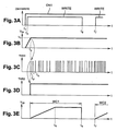
図3A〜図3Eは、メモリを書き込むサイクルWC1、WC2、...を含むメモリの書き込み段階の間の信号ON1、WRITE、THR1、フラグTHR2、及び電圧Vhv、Vppの特徴を示す。信号ON1及びWRITEは、図3Aにおいて示され、電圧Vhvは、図3Bにおいて示され(しきい値Vcの周辺への調整によって引き起こされた電圧Vhvの変化は示されない)、信号THR1は、(ここでは、電圧Vhvの検出信号及び調整信号として)図3Cにおいて示され、フラグTHR2は、図3Dにおいて示されると共に、傾斜波発生器であるスイッチ回路SCTによって供給される電圧Vppは、図3Eにおいて示される。 3A to 3E show the cycles WC1, WC2,. . . The characteristics of the signals ON1, WRITE, THR1, flag THR2, and voltages Vhv, Vpp during the write phase of the memory including are shown. Signals ON1 and WRITE are shown in FIG. 3A, voltage Vhv is shown in FIG. 3B (changes in voltage Vhv caused by adjustments around threshold Vc are not shown), and signal THR1 is (here In FIG. 3C, the flag THR2 is shown in FIG. 3D, and the voltage Vpp supplied by the switch circuit SCT, which is a ramp generator, is shown in FIG. 3E. It is.
“書き込みサイクル”WC1、WC2は、1つ以上のメモリセルに関する消去またはプログラミングのサイクルを意味し、“書き込み段階”は、データを格納するために必要な全ての消去及びプログラミングのサイクルを含む期間を意味する。例えば、もしメモリMEMが8ビットワードによって消去可能であると共に、8ビットワードによってプログラム可能で、書き込まれるべきデータがワードある場合、ワードを書き込む段階は、8つのメモリセルを消去するサイクル(集合的な消去サイクル、メモリセルに対する“0”の書き込み)と、“1”を受け取ることを意図されたメモリセルの集合的なプログラミングのサイクルとを含む。もしメモリMEMがページ消去可能(page-erasable)(ワードライン)か、またはセクタ消去可能であり、かつバイトによってプログラム可能である場合、そして、もし書き込まれるべきデータが同じセクタまたは同じページに属するいくつかのワードを含む場合、ワードを書き込む段階は、全セクタの、もしくは全ページの集合的な消去のサイクルと、書き込まれるべきワードと同数のプログラミングサイクルとを含む。 “Write cycle” WC1, WC2 refers to an erase or programming cycle for one or more memory cells, and “write phase” refers to a period that includes all the erase and programming cycles required to store data. means. For example, if the memory MEM is erasable with an 8-bit word and is programmable with an 8-bit word, and there is data to be written, writing the word is a cycle of erasing eight memory cells (collectively Erase cycle, “0” write to the memory cell) and collective programming cycle of the memory cell intended to receive “1”. If the memory MEM is page-erasable (wordline) or sector erasable and programmable by bytes, and if the data to be written belongs to the same sector or page If so, writing the word includes a collective erase cycle of all sectors or pages and the same number of programming cycles as the word to be written.
第1の書き込みサイクルWC1に先行する時刻“t0”、例えば消去サイクルにおいて、信号ON1及びWRITEは、“0”であり、電圧Vhvは、ゼロに等しく、信号THR1は、“0”に等しく、そしてフラグTHR2は、(フリップフロップFF1の入力端子RESETに作用する)信号ON1によって“0”に保持される。時刻“t1”において、ユニットCTU2は、信号ON1を“1”にセットすると共に、電圧Vhvは、増加し始める。時刻“t2”において、ユニットCTU2は、信号WRITEを“1”にセットするが、しかしスイッチ回路SCTは、フラグTHR2が“0”に等しいと共に、回路SCTの制御入力端子に対する信号WRITEの印加を抑制するので、遮断された状態を維持する。時刻“t3”において、電圧Vhvは、しきい値Vcに到達すると共に、ブースタ回路が電圧を印加されたので、同様にフラグTHR2が“1”になるように、信号THR1は、初めて“1”になる。回路SCTは、それ自身を始動すると共に、電圧Vppの傾斜波形がメモリMEMに印加される。同時に、信号ON1は、ブースタ回路の入力端子において抑制されると共に、高電圧Vhvは、減少する。時刻“t3’”において、電圧Vhvは、再びしきい値Vcより下に行き、そして信号THR1は、“0”に戻る。時刻“t4”において、電圧Vhvは、しきい値Vcに到達すると共に、信号THR1は、“1”に戻り、その後、時刻“t4’”において“0”になる等...、電圧Vhvの調整によって引き起こされたこれらの変化は、信号ON1が“1”を維持する限り、書き込み段階の間ずっと“1”を維持するフラグTHR2に影響を及ぼさない。時刻“t5”において、電圧Vppは、Vc(または、もし回路STCが電圧Vmの電圧Vhvへの減少を強制するならば、“Vc−Vm”)に等しい水平状態に到達すると共に、ユニットCTU2が、信号ON1を“1”にする一方、信号WRITEを“0”にセットする場合、書き込みサイクルWC1の終了を示す時刻“t6”まで、水平状態の周辺で安定した状態を維持する。信号THR1は、高電圧Vhvを調整するために、“0”から“1”及び“1”から“0”に交互に移行し続けると共に、フラグTHR2は、“1”を維持する。時刻“t7”において、ユニットCTU2は、信号WRITEを“1”に戻すようにセットすると共に、第2の書き込みサイクルWC2、例えばプログラミングサイクルが開始される。ここでは、フラグTHR2は、サイクルWC2の開始から“1”であると共に、書き込み段階の間ずっと“1”を維持する。 At time “t0” preceding the first write cycle WC1, eg, in the erase cycle, the signals ON1 and WRITE are “0”, the voltage Vhv is equal to zero, the signal THR1 is equal to “0”, and The flag THR2 is held at “0” by the signal ON1 (acting on the input terminal RESET of the flip-flop FF1). At time “t1”, the unit CTU2 sets the signal ON1 to “1”, and the voltage Vhv starts to increase. At time “t2”, the unit CTU2 sets the signal WRITE to “1”, but the switch circuit SCT suppresses the application of the signal WRITE to the control input terminal of the circuit SCT while the flag THR2 is equal to “0”. As a result, the blocked state is maintained. At time “t3”, the voltage Vhv reaches the threshold value Vc and the booster circuit is applied with the voltage. Similarly, the signal THR1 is “1” for the first time so that the flag THR2 becomes “1”. become. The circuit SCT starts itself and a ramp waveform of the voltage Vpp is applied to the memory MEM. At the same time, the signal ON1 is suppressed at the input terminal of the booster circuit, and the high voltage Vhv decreases. At time “t3 ′”, the voltage Vhv again goes below the threshold value Vc, and the signal THR1 returns to “0”. At time “t4”, the voltage Vhv reaches the threshold value Vc, and the signal THR1 returns to “1”, and then becomes “0” at time “t4 ′”, etc. . . These changes caused by the adjustment of the voltage Vhv do not affect the flag THR2, which remains “1” throughout the write phase, as long as the signal ON1 remains “1”. At time “t5”, voltage Vpp reaches a horizontal state equal to Vc (or “Vc−Vm” if circuit STC forces the voltage Vm to decrease to voltage Vhv) and unit CTU2 is When the signal ON1 is set to “1” while the signal WRITE is set to “0”, the stable state is maintained around the horizontal state until time “t6” indicating the end of the write cycle WC1. The signal THR1 continues to alternately shift from “0” to “1” and “1” to “0” in order to adjust the high voltage Vhv, and the flag THR2 maintains “1”. At time “t7”, unit CTU2 sets signal WRITE back to “1” and a second write cycle WC2, eg, a programming cycle, is started. Here, the flag THR2 is “1” from the start of the cycle WC2, and maintains “1” throughout the write phase.
図4は、制御ユニットCT2による書き込み段階の実行、及び高電圧Vhvの起こり得る障害を診断するためのフラグTHR2の使用を説明する図である。ステップS100の間、ユニットCTU2は、リーダRD1から、命令“[WRITE][DTW][ADW]”を受信する。ステップS110の間、ユニットCTU2は、ブースタ回路を活性化するために、信号ON1を“1”にセットする(上記の時刻“t1”)と共に、メモリにデータDTWとアドレスADWとを印加する。ステップS120の間、ユニットCTU2は、信号WRITEを“1”にセットする(上記の時刻“t2”)。ステップS110及びS120は、信号ON1を“1”に維持したままで、実行されるべき書き込みサイクルCW1、CW2...の数と同じ数だけ忠実に繰り返され得る。 FIG. 4 is a diagram for explaining the execution of the write phase by the control unit CT2 and the use of the flag THR2 for diagnosing a possible failure of the high voltage Vhv. During step S100, the unit CTU2 receives the command “[WRITE] [DTW] [ADW]” from the reader RD1. During step S110, in order to activate the booster circuit, the unit CTU2 sets the signal ON1 to “1” (the above time “t1”) and applies the data DTW and the address ADW to the memory. During step S120, the unit CTU2 sets the signal WRITE to “1” (the above time “t2”). Steps S110 and S120 are the write cycles CW1, CW2,. . . Can be repeated faithfully as many times as
一度書き込み段階が終了されれば、ユニットCTU2は、ステップS130の間にフラグTHR2を検査し、もしフラグTHR2が“1”に等しいならば、書き込み段階は、正常に発生したと考えられると共に、ユニットCTU2は、それが新しい命令を待つステップS140(“WAIT”)にジャンプする。 Once the write phase is complete, unit CTU2 checks flag THR2 during step S130, and if flag THR2 is equal to "1", the write phase is considered to have occurred normally and unit CTU2 CTU2 jumps to step S140 ("WAIT") where it waits for a new instruction.
変形において、ユニットCTU2は、それがメモリに書き込んだデータを読み取ると共に、書き込まれたデータが実際に命令に含まれるデータであることをリーダRD1が確認し得るように、次のステップS140へジャンプする前に、それらを命令の実行を確認するためのメッセージに含めて送り返す。 In a variant, the unit CTU2 jumps to the next step S140 so that the reader RD1 can read the data it has written to the memory and confirm that the written data is actually the data contained in the instruction. Before they are sent back in a message confirming execution of the instruction.
もしフラグTHR2が“0”に等しいならば、それは、高電圧Vhvが臨界しきい値に到達しなかったということ、そしてそのメモリは書き込まれなかったということを意味する。ユニットCTU2は、それが失敗メッセージ“WRITEFAIL”を送信するステップS150にジャンプする。前述のように、ユニットCTU2は、破損したデータが書き込まれなかったことを証明し得るように、命令に現れる読み取りアドレスADRにおけるメモリ内のデータを読み取るため、及びそれらをメッセージWRITEFAILによってリーダRD1に送り返すために提供され得る。しかしながら、本発明に基づくフラグTHR2の利点は、集積回路が、電圧Vccの観測ではなく電圧Vhvの観測に基づく信頼できる失敗診断のおかげで、メモリエリアを再度読み取る必要なく、書き込み失敗メッセージを迅速に送信することを可能にすることである。 If the flag THR2 is equal to “0”, it means that the high voltage Vhv has not reached the critical threshold and that the memory has not been written. Unit CTU2 jumps to step S150 where it sends a failure message “WRITEFAIL”. As mentioned above, unit CTU2 reads the data in memory at read address ADR appearing in the instruction and sends them back to reader RD1 by message WRITEFAIL so that it can prove that the corrupted data was not written. Can be provided for. However, the advantage of the flag THR2 according to the present invention is that the integrated circuit can quickly write a write failure message without having to read the memory area again, thanks to a reliable failure diagnosis based on the observation of the voltage Vhv rather than the observation of the voltage Vcc. It is possible to transmit.
自動的に傾斜波発生器回路SCTの活性化を抑制するためのインジケータフラグTHR2の使用は、集積回路IC2が、クロック信号CKによって達成される固定の順序付けに従う書き込みサイクルを測定する有限の状態機械を含むワイヤードロジック制御ユニットCTUを装備している場合に、本発明の特に有利な特徴であるということに、当業者は注目することになる。ワイヤードロジック制御ユニットの供給は、大規模なアプリケーションに対して低コストの集積回路を組み立てることを可能にする。 The use of the indicator flag THR2 to automatically suppress the activation of the ramp generator circuit SCT makes it possible for the integrated circuit IC2 to use a finite state machine that measures the write cycle according to the fixed ordering achieved by the clock signal CK. Those skilled in the art will note that this is a particularly advantageous feature of the present invention when equipped with a wired logic control unit CTU. The supply of wired logic control units allows low cost integrated circuits to be assembled for large scale applications.
しかしながら、本発明は、制御ユニットの“知能”のレベル及び適応性に従って、様々な実施例が可能である。例えば、マイクロプロセッサ制御ユニットは、活性化信号WRITEをスイッチ回路SCTに印加する前に、フラグTHHR2を検査することができる。そのような場合、フラグTHR2による信号WRITEの抑制は、必要ではない。制御ユニットは、タイマによって測定された期間の間にフラグTHR2が“1”になるのを待つと共に、もし電圧Vhvが臨界しきい値Vcに到達することなく期間が終了するならば、制御ユニットは、書き込みサイクルをキャンセルすると共に、メッセージWRITEFAILを送信する。 However, the present invention is capable of various embodiments according to the level of intelligence and adaptability of the control unit. For example, the microprocessor control unit can check the flag THHR2 before applying the activation signal WRITE to the switch circuit SCT. In such a case, suppression of the signal WRITE by the flag THR2 is not necessary. The control unit waits for the flag THR2 to become “1” during the period measured by the timer, and if the period ends without the voltage Vhv reaching the critical threshold Vc, the control unit , Cancel the write cycle and send the message WRITEFAIL.
図5は、チャージポンプPMPの標準的な実施例を示す。それは、各コンデンサのアノードが、ダイオードD1、D2...Dn−1によって、次の階層のコンデンサのアノードに連結されると共に、奇数の階層の各コンデンサのカソードが、ポンプ信号H1を受信し、偶数の階層の各コンデンサのカソードが、ポンプ信号H2を受信する、並列に接続されたコンデンサC1、C2...Cnを備える。ダイオードDnは、最後のコンデンサのアノードを電圧Vhvを供給する出力のコンデンサChvに連結すると共に、電圧Vccは、ダイオードD0を通して、第1のコンデンサC1のアノードに印加される。信号H1がプルアップされて、信号H2がプルダウンされる場合、信号H2がプルアップされて信号H1がプルダウンされる先行する半周期の間に電荷が蓄積される奇数の階層の各コンデンサは、直後に連結される偶数の階層のコンデンサに放電する。信号H2がプルアップされて、信号H1がプルダウンされる場合、信号H1がプルアップされて信号H2がプルダウンされる先行する半周期の間に電荷が蓄積される偶数の階層の各コンデンサは、直後に連結される奇数の階層のコンデンサに放電する。 FIG. 5 shows a standard embodiment of the charge pump PMP. That is, the anode of each capacitor is connected to diodes D1, D2,. . . The cathodes of the capacitors in the odd layers receive the pump signal H1, and the cathodes of the capacitors in the even layers receive the pump signal H2. In parallel, capacitors C1, C2. . . Cn is provided. The diode Dn connects the anode of the last capacitor to the output capacitor Chv supplying the voltage Vhv, and the voltage Vcc is applied to the anode of the first capacitor C1 through the diode D0. When the signal H1 is pulled up and the signal H2 is pulled down, each capacitor in the odd-numbered layer in which charge is accumulated during the preceding half cycle in which the signal H2 is pulled up and the signal H1 is pulled down Are discharged to an even number of capacitors connected to. When the signal H2 is pulled up and the signal H1 is pulled down, each capacitor in the even layer in which charge is accumulated during the preceding half cycle in which the signal H1 is pulled up and the signal H2 is pulled down The capacitor is discharged to an odd number of layers connected to the capacitor.
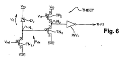
図6は、検出回路THDETの実施例を示す。検出回路THDETは、そのソース端子がグランド(アース)に連結されたNMOSトランジスタTN1のドレイン端子に連結されたダイオードによって形成される入力ステージを備える。ダイオードDdは、逆向きに搭載されると共に、電圧Vhvを受け取る。トランジスタTN1は、そのゲート端子Gにおいて、好ましくは温度補償された固定のバイアス電圧Vrefを受け取る。ダイオードDdは、逆方向電圧Vdを有していると共に、トランジスタは、電圧Vrefによって課されたドレーン−ソース間電圧Vdsを有している。トランジスタTN1のドレインに位置するノードN1は、グランドと連結されたソース端子Sを有するNMOSトランジスタTN2のゲート端子に連結される。このトランジスタのドレイン端子Dは、その出力端子が検出信号THR1を供給する反転ゲート回路INV1の入力端子に連結されるノードN2を形成する。ノードN2は、そのソース端子Sが電圧Vccを受け取ると共に、そのゲート端子が電圧V2を受け取るPMOSトランジスタTP2によってプルアップされる。電圧Vhvが、ここでは“Vd+Vds”に等しいしきい値Vcに到達するとき、入力ステージは、導通することになると共に、ノードN1は、ハイインピーダンス電位から電位Vdsになる。トランジスタTN2は、導通することになると共に、ノードN2は、“1”(Vcc)から“0”(グランド)になる。信号THR1は、“1”になる。 FIG. 6 shows an embodiment of the detection circuit THDET. The detection circuit THDET includes an input stage formed by a diode connected to the drain terminal of the NMOS transistor TN1 whose source terminal is connected to ground (earth). The diode Dd is mounted in the reverse direction and receives the voltage Vhv. Transistor TN1 receives at its gate terminal G a fixed bias voltage Vref, preferably temperature compensated. The diode Dd has a reverse voltage Vd and the transistor has a drain-source voltage Vds imposed by the voltage Vref. A node N1 located at the drain of the transistor TN1 is connected to a gate terminal of an NMOS transistor TN2 having a source terminal S connected to the ground. The drain terminal D of this transistor forms a node N2 whose output terminal is connected to the input terminal of the inverting gate circuit INV1 which supplies the detection signal THR1. Node N2 is pulled up by PMOS transistor TP2 whose source terminal S receives voltage Vcc and whose gate terminal receives voltage V2. When the voltage Vhv reaches a threshold value Vc equal to “Vd + Vds” in this case, the input stage becomes conductive, and the node N1 changes from the high impedance potential to the potential Vds. The transistor TN2 becomes conductive, and the node N2 changes from “1” (Vcc) to “0” (ground). The signal THR1 becomes “1”.
図7は、それぞれゲート回路がもう一方のゲート回路の入力端子と連結された出力端子を有する2つのゲート回路NOR1、NOR2(ノアゲート回路)を用いたフリップフロップFF1の実施例を示す。ゲート回路NOR1のもう一方の入力端子は、フリップフロップの入力端子SETを形成すると共に、信号THR1を受け取る。ゲート回路NOR2のもう一方の入力端子は、フリップフロップの入力端子RESETを形成すると共に、上述のように、信号“/ON1”を受け取る。ゲート回路NOR2の出力端子は、フラグTHR2を供給する。任意に、ゲート回路NOR2は、フリップフロップの入力端子RESET’を形成すると共に、電源投入毎に集積回路によって生成されるPOR(パワーオンリセット)信号を受け取る第3の入力端子を備える。 FIG. 7 shows an embodiment of a flip-flop FF1 using two gate circuits NOR1 and NOR2 (nor gate circuits) each having an output terminal connected to the input terminal of the other gate circuit. The other input terminal of the gate circuit NOR1 forms the input terminal SET of the flip-flop and receives the signal THR1. The other input terminal of the gate circuit NOR2 forms the input terminal RESET of the flip-flop and receives the signal “/ ON1” as described above. The output terminal of the gate circuit NOR2 supplies a flag THR2. Optionally, the gate circuit NOR2 forms a flip-flop input terminal RESET 'and has a third input terminal that receives a POR (Power On Reset) signal generated by the integrated circuit each time the power is turned on.
図8は、メモリMEMの実施例を概略的に示す。メモリMEMは、メモリアレイMA、アドレスデコーダADEC、プログラミング回路PCT、選択回路SCT、及び読み取り回路RCTを備える。メモリアレイMAは、水平ライン及び垂直のラインに従って配置されると共に、ワードラインWLiとビットラインBLjに連結された、電気的に消去可能で、かつプログラム可能なメモリセルCi、jを備える。プログラミング回路PCTは、デコーダADECによって供給された信号COLSELによって選択されると共に、メモリアレイに書き込まれるべきデータDTWを受け取る、メモリアレイのビットラインに連結された消去−プログラミング安全装置(erase-programming locks)(図示せず)を備える。読み取り回路RCTは、選択回路SCTを通してメモリアレイMAのビットラインに連結された1つ以上のセンス増幅器を備えると共に、メモリアレイにおいて読み取られたデータDTRを供給する。 FIG. 8 schematically shows an embodiment of the memory MEM. The memory MEM includes a memory array MA, an address decoder ADEC, a programming circuit PCT, a selection circuit SCT, and a reading circuit RCT. The memory array MA includes electrically erasable and programmable memory cells Ci, j that are arranged according to a horizontal line and a vertical line and are connected to the word line WLi and the bit line BLj. The programming circuit PCT is selected by the signal COLSEL supplied by the decoder ADEC and receives the data DTW to be written to the memory array and is connected to an erase-programming locks coupled to the bit lines of the memory array. (Not shown). The read circuit RCT includes one or more sense amplifiers connected to the bit lines of the memory array MA through the selection circuit SCT and supplies data DTR read in the memory array.
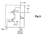
図9は、ビットbi、jがメモリアレイに格納されることを可能にする、電気的に消去可能で、かつプログラム可能なメモリセルCi、jの実施例を示す。メモリセルは、ここではNMOSタイプである、フローティングゲートトランジスタFGTと、アクセストランジスタATとを備える。アクセストランジスタは、ビットラインBLjに連結されたドレイン端子D、ワードラインWLiに連結されたゲート端子G、及びトランジスタFGTのドレイン端子Dに連結されたソース端子Sを備えている。更に、トランジスタFGTは、フローティングゲート端子FG、制御ゲートラインCGLに連結された制御ゲート端子CG、及びソースラインSLiに連結されたソース端子Sを備える。メモリセルCi、jは、例えば電圧Vppを、アクセストランジスタATを介して、トランジスタFGTのドレイン端子Dに印加すると共に、より低い値の電圧、例えば0[V]を、その制御ゲート端子CGに印加することによって、プログラムされた状態にセットされる。電荷が、トンネル効果によってフローティングゲート端子FGに注入されると共に、一般的に負の状態になるトランジスタFGTのスレショルド電圧Vtを下げる。メモリセルCi、jは、例えば電圧Vppを、トランジスタFGTの制御ゲート端子CGに印加すると共に、より低い値の電圧、例えば0[V]を、そのソース端子Sに印加することによって、消去された状態にセットされる。電荷は、トンネル効果によってフローティングゲート端子FGから抽出されると共に、トランジスタFGTのスレショルド電圧は、一般的に正の状態になるように増加する。 FIG. 9 shows an example of an electrically erasable and programmable memory cell Ci, j that allows bits bi, j to be stored in the memory array. The memory cell includes a floating gate transistor FGT and an access transistor AT, which are of the NMOS type here. The access transistor includes a drain terminal D connected to the bit line BLj, a gate terminal G connected to the word line WLi, and a source terminal S connected to the drain terminal D of the transistor FGT. The transistor FGT further includes a floating gate terminal FG, a control gate terminal CG connected to the control gate line CGL, and a source terminal S connected to the source line SLi. The memory cell Ci, j applies, for example, the voltage Vpp to the drain terminal D of the transistor FGT via the access transistor AT, and applies a lower value voltage, for example, 0 [V] to the control gate terminal CG. To set the programmed state. Electric charges are injected into the floating gate terminal FG by the tunnel effect, and the threshold voltage Vt of the transistor FGT that is generally in a negative state is lowered. The memory cell Ci, j is erased, for example, by applying the voltage Vpp to the control gate terminal CG of the transistor FGT and applying a lower value voltage, eg 0 [V], to its source terminal S. Set to state. The charge is extracted from the floating gate terminal FG by the tunnel effect, and the threshold voltage of the transistor FGT generally increases so as to be in a positive state.
メモリセルCi、jの読み取りは、ビットラインBLjとアクセストランジスタATとを介してトランジスタFGTのドレイン端子Dに連結されたセンス増幅器RCTjによって保証される。増幅器RCTjは、読み取り電圧VreadがトランジスタFGTの制御ゲート端子CGに印加されると共に、そのソースラインがグランドに連結される間、ビットラインにバイアス電圧Vpolを印加する。もしトランジスタFGTがプログラムされた状態にあるならば、メモリセルは、導通していると共に、読み取り電流Ireadは、ビットラインBLjを流れる決定されたしきい値電流を超えている。増幅器RCTjは、その場合に、その値が慣例により定義された例えば“1”である、ビットbi、jを供給する。もしトランジスタFGTが消去された状態にあるならば、メモリセルは、導通していないか、または僅かに導通している状態であると共に、増幅器RCTjは、逆の値である例えば“0”に等しいビットbi、jを供給する。 Reading of the memory cell Ci, j is ensured by a sense amplifier RCTj connected to the drain terminal D of the transistor FGT via the bit line BLj and the access transistor AT. The amplifier RCTj applies the bias voltage Vpol to the bit line while the read voltage Vread is applied to the control gate terminal CG of the transistor FGT and the source line is connected to the ground. If transistor FGT is in a programmed state, the memory cell is conducting and read current Iread exceeds the determined threshold current flowing through bit line BLj. The amplifier RCTj then supplies the bits bi, j whose value is eg “1” as defined by convention. If transistor FGT is in an erased state, the memory cell is not conducting or slightly conducting, and amplifier RCTj is equal to the opposite value, eg, “0”. Provide bits bi, j.
トンネル効果によってセルを電気的に消去可能であると共に、プログラム可能である、このメモリEEPROMの使用は、トンネル効果による電荷の注入及び抽出が非常に低い電流によって行われるので、電荷の注入がホットキャリヤの注入によって行われると共に、かなりのセル電流を必要とするメモリと異なり、有利である。従って、電圧Vhvの減衰がある場合においてさえも、臨界しきい値Vcに到達するとすぐに、書き込みプロセスが通常は適切に進展しなければならないことに照らして、このメモリは本発明の基本原理を満足する。実際には、そして上述のことから明らかなように、しきい値Vcは、好ましくはブースタ回路の調整しきい値に等しいか、またはブースタ回路の調整しきい値に近い、一般的にはこれらのメモリセルを作るために使用された技術に基づくと約10〜15[V]に選択される。 The use of this memory EEPROM, in which the cells can be electrically erased by the tunneling effect and is programmable, the charge injection and extraction by the tunneling effect is performed with a very low current, so that the charge injection is a hot carrier. This is advantageous, unlike memories that require a significant cell current. Thus, even in the presence of voltage Vhv decay, as soon as the critical threshold Vc is reached, this memory is based on the basic principle of the present invention in the light of the fact that the writing process usually has to proceed appropriately. Satisfied. In practice, and as is apparent from the above, the threshold Vc is preferably equal to or close to the booster circuit adjustment threshold, generally these Based on the technology used to make the memory cell, it is selected to be about 10-15 [V].
高電圧Vhvを監視するための手段、及びインジケータフラグTHR2を管理するための手段が、様々な実施例として可能であることは、当業者には明らかである。本発明は、更にいくつかのアプリケーションが可能であると共に、電気的結合によって動作する非接触式UHF回路だけを対象としない。本発明は、例えば誘導結合を使用する集積回路に適用されると共に、その電源がメモリセルをプログラミングまたは消去する段階の間の失敗の影響を受けやすい、あらゆる集積回路またはトランスポンダに全体的に適用される。 It will be apparent to those skilled in the art that means for monitoring the high voltage Vhv and means for managing the indicator flag THR2 are possible in various embodiments. The present invention is capable of several more applications and does not cover only contactless UHF circuits that operate by electrical coupling. The invention applies generally to any integrated circuit or transponder, for example applied to an integrated circuit using inductive coupling, and whose power supply is susceptible to failure during the phase of programming or erasing a memory cell. The
IC1、IC2 集積回路
AC ダイポールアンテナ回路
CICT 通信用インタフェース回路
CTU1、CTU2 制御ユニット
MEM 不揮発性メモリ
HVCT 電荷蓄積ブースタ回路
CK クロック信号
OSC 発振器
Vcc 電源電圧
Vhv 高電圧
E 電界
W1、W2 ダイポールを形成するワイヤ
RD1 リーダ
S1、S2 アンテナ信号
PSCT 電源回路
MCT 変調回路
DCT 復調回路
DTx 送信されるべきデータ
S(DTx) インピーダンス変調信号
DTr 伝送されたデータ
PMP チャージポンプ
HGEN チャージポンプの励磁を保証する回路
H1、H2 低周波数ポンプ信号
SCT スイッチ回路
ADR 読み取りアドレス
ADW 書き込みアドレス
DTW 書き込まれるべきデータ
DTR メモリにおいて読まれたデータ
THDET しきい値検出回路
THR1 検出信号
THR2 インジケータフラグ
FF1 フリップフロップ(揮発性の記憶手段/メモリポイント)
A1、A2 ゲート回路
Vpp 傾斜波形で供給された高電圧
ON1、“/ON1”、WRITE 信号
D1、D2...Dn ダイオード
C1、C2...Cn コンデンサ
Chv 出力のコンデンサ
TN1 NMOSトランジスタ
Dd ダイオード
Vref 固定のバイアス電圧
Vd ダイオードの逆方向電圧
Vds ドレーン−ソース間電圧
N1、N2 ノード
V2 電圧
TN2 NMOSトランジスタ
INV1 反転ゲート回路
TP2 PMOSトランジスタ
NOR1、NOR2 ノアゲート回路
POR パワーオンリセット信号
MA メモリアレイ
ADEC アドレスデコーダ
PCT プログラミング回路
SCT 選択回路
RCT 読み取り回路
COLSEL 信号
WLi ワードライン
BLj ビットライン
Ci、j メモリセル
FGT フローティングゲートトランジスタ
AT アクセストランジスタ
CGL 制御ゲートライン
SLi ソースライン
RCTj センス増幅器
Vread 読み取り電圧
Vpol バイアス電圧
Iread 読み取り電流
IC1, IC2 Integrated circuit AC Dipole antenna circuit CICT Communication interface circuit CTU1, CTU2 Control unit MEM Non-volatile memory HVCT Charge storage booster circuit CK Clock signal OSC Oscillator Vcc Power supply voltage Vhv High voltage E Electric field W1, W2 Wire forming dipole RD1 Reader S1, S2 Antenna signal PSCT Power supply circuit MCT Modulation circuit DCT Demodulation circuit DTx Data to be transmitted S (DTx) Impedance modulation signal DTr Transmitted data PMP Charge pump HGEN Circuits that guarantee charge pump excitation H1, H2 Low frequency Pump signal SCT switch circuit ADR read address ADW write address DTW Data to be written DTR Data read in the memory HDET threshold detection circuit THR1 detection signal THR2 indicator flag FF1 flipflop (volatile storage means / memory point)
A1, A2 Gate circuit Vpp High voltage ON1, “/ ON1” supplied with ramp waveform, WRITE signal D1, D2. . . Dn diodes C1, C2. . . Cn Capacitor Chv Output Capacitor TN1 NMOS Transistor Dd Diode Vref Fixed Bias Voltage Vd Diode Reverse Voltage Vds Drain-Source Voltage N1, N2 Node V2 Voltage TN2 NMOS Transistor INV1 Inverted Gate Circuit TP2 PMOS Transistor NOR1, NOR2 NOR Gate Circuit Power-on reset signal MA memory array ADEC address decoder PCT programming circuit SCT selection circuit RCT reading circuit COLSEL signal WLi word line BLj bit line Ci, j memory cell FGT floating gate transistor AT access transistor CGL control gate line SLi source line RCTj sense amplifier Vread Read voltage Vp ol Bias voltage Iread Read current
Claims (21)
−インジケータフラグ(THR2)を記憶するための揮発性の記憶手段(FF1)と、
−前記ブースタ回路を活性化した後で前記高電圧(Vhv)が最初に臨界しきい値(Vc)に到達するときに、前記インジケータフラグ(THR2)の値を変更するための手段(THDET、THR1、FF1)と
を備えることを特徴とする集積回路。 An electrically programmable non-volatile data memory (MEM), and a charge storage booster circuit (HVCT, PMP, HGEN) for supplying a high voltage (Vhv) necessary for writing data (DTW) to the memory; A passive non-contact integrated circuit (IC2) comprising:
A volatile storage means (FF1) for storing the indicator flag (THR2);
Means (THDET, THR1) for changing the value of the indicator flag (THR2) when the high voltage (Vhv) first reaches a critical threshold value (Vc) after activating the booster circuit; , FF1).
前記ブースタ回路を活性化した後で前記高電圧が前記臨界しきい値(Vc)に到達しなかったならば、前記スイッチ回路(SCT)が前記メモリ(MEM)に前記高電圧を印加することを回避するための手段(A2)と
を備えることを特徴とする請求項1に記載の集積回路。 A switch circuit (SCT) for applying the high voltage (Vhv) to the memory (MEM);
If the high voltage does not reach the critical threshold value (Vc) after activating the booster circuit, the switch circuit (SCT) applies the high voltage to the memory (MEM). The integrated circuit according to claim 1, characterized in that it comprises means (A2) for avoiding.
ことを特徴とする請求項2に記載の集積回路。 The integrated circuit according to claim 2, wherein the switch circuit (SCT) includes a ramp generator for gradually supplying the high voltage (Vhv) to the memory (MEM).
ことを特徴とする請求項1から請求項3のいずれか一項に記載の集積回路。 An instruction for writing the data (DTW) to the memory (MEM) is configured to be executed, and the high voltage (Vhv) is set to the critical threshold (Vc) during execution of the instruction to write. 4. A control unit (CTU2) for transmitting a specific information message (WRITEFAIL) when the flag (THR2) indicates that the information has not been reached. An integrated circuit according to any one of the above.
−前記ブースタ回路(HVCT、HGEN、PMP)に、それが前記高電圧(Vhv)を生成するように、活性化信号(ON1=1)を印加する動作と、
−前記メモリに書き込みアドレス(ADW)及び書き込まれるべきデータ(DTW)を印加する動作と、
−前記メモリに対して前記高電圧(Vhv)を供給するスイッチ回路(SCT)に活性化信号(WRITE=1)を印加する動作と
を無条件に実行するように構成された制御ユニット(CTU2)を備える
ことを特徴とする請求項1から請求項4のいずれか一項に記載の集積回路。 In response to an instruction to write the data (DTW) to the memory (MEM), the following:
-Applying an activation signal (ON1 = 1) to the booster circuit (HVCT, HGEN, PMP) so that it generates the high voltage (Vhv);
-Applying a write address (ADW) and data to be written (DTW) to the memory;
A control unit (CTU2) configured to unconditionally execute an operation of applying an activation signal (WRITE = 1) to a switch circuit (SCT) for supplying the high voltage (Vhv) to the memory The integrated circuit according to claim 1, further comprising:
−前記ブースタ回路(HVCT、HGEN、PMP)に、それが前記高電圧(Vhv)を生成するように、活性化信号(ON1=1)を印加する動作と、
−前記メモリに書き込みアドレス(ADW)及び書き込まれるべきデータ(DTW)を印加する動作と、
−もし前記高電圧が前記臨界しきい値(Vc)に到達する場合、前記メモリに対して前記高電圧(Vhv)を供給するスイッチ回路(SCT)に活性化信号(WRITE=1)を印加する動作と、
−もし前記高電圧が判定された期間の終りに前記臨界しきい値(Vc)に到達しなかった場合、前記スイッチ回路(SCT)に前記活性化信号(WRITE=1)を印加しないと共に、前記高電圧(Vhv)が前記メモリに印加されなかったことを示す特定の情報のメッセージ(WRITEFAIL)を送信する動作と
を実行するように構成された制御ユニット(CTU2)を備える
ことを特徴とする請求項1または請求項2のいずれか一項に記載の集積回路。 When receiving an instruction to write the data (DTW) to the memory (MEM),
-Applying an activation signal (ON1 = 1) to the booster circuit (HVCT, HGEN, PMP) so that it generates the high voltage (Vhv);
-Applying a write address (ADW) and data to be written (DTW) to the memory;
If the high voltage reaches the critical threshold value (Vc), an activation signal (WRITE = 1) is applied to the switch circuit (SCT) that supplies the high voltage (Vhv) to the memory Operation and
-If the critical threshold (Vc) is not reached at the end of the period during which the high voltage is determined, the activation signal (WRITE = 1) is not applied to the switch circuit (SCT), and And a control unit (CTU2) configured to perform a specific information message (WRITEFAIL) indicating that a high voltage (Vhv) has not been applied to the memory. The integrated circuit as described in any one of Claim 1 or Claim 2.
ことを特徴とする請求項1から請求項6のいずれか一項に記載の集積回路。 The high voltage is monitored, and a detection signal (THR1) indicating whether the high voltage (Vhv) is lower than the critical threshold value (Vc) or higher than the critical threshold value (Vc). The integrated circuit according to any one of claims 1 to 6, further comprising a detection circuit (THDET) for supplying
ことを特徴とする請求項1から請求項7のいずれか一項に記載の集積回路。 Whenever the high voltage (Vhv) is higher than or equal to the adjustment threshold value (Vc), the adjustment signal (THR1) of the booster circuit having a valid value (1) is supplied. The integrated circuit according to any one of claims 1 to 7, further comprising a regulator circuit (THDET, A1).
ことを特徴とする請求項8に記載の集積回路。 9. The integrated circuit according to claim 8, wherein the critical threshold value is equal to the adjustment threshold value (Vc).
ことを特徴とする請求項7から請求項9のいずれか一項に記載の集積回路。 The integrated circuit according to claim 7, wherein the adjustment signal (THR1) and the detection signal (THR1) are the same.
ことを特徴とする請求項1から請求項9のいずれか一項に記載の集積回路。 A first control input for the indicator flag (THR2) to provide the flag (THR2) with a first value meaning that the high voltage (Vhv) has reached the critical threshold value (Vc) Terminal (SET) and a second control input for providing the flag (THR2) with a second value that means that the high voltage (Vhv) has not reached the critical threshold (Vc) 10. The integrated circuit according to claim 1, wherein the integrated circuit is stored by a flip-flop (FF1) having a terminal (RSET).
ことを特徴とする請求項7または請求項11のいずれか一項に記載の集積回路。 The integrated circuit according to claim 7 or 11, wherein the first control input terminal (SET) of the flip-flop receives the detection signal (THR1).
ことを特徴とする請求項11または請求項12のいずれか一項に記載の集積回路。 The second control input terminal (RSET) of the flip-flop is a signal (/ ON1) for deactivating the booster circuit and / or a signal (POR) for resetting the integrated circuit. 13. The integrated circuit according to claim 11, wherein at least one of the signals is received.
携帯用の担体と、
前記携帯用の担体に搭載されるか、もしくは前記携帯用の担体に統合される請求項1から請求項13のいずれか一項に記載の集積回路(IC2)と
を備えることを特徴とする携帯用電子体。 A portable electronic body of the type of chip card or electronic tag,
A portable carrier;
A portable device comprising the integrated circuit (IC2) according to any one of claims 1 to 13, which is mounted on the portable carrier or integrated with the portable carrier. Electronic body.
−集積回路の揮発性の記憶手段(FF1)内のインジケータフラグ(THR2)を初期化する段階と、
−前記メモリにデータ(DTW)を書き込むために必要な高電圧(Vhv)を供給する電荷蓄積ブースタ回路(HVCT、PMP、HGEN)を活性化する(ON1=1)段階と、
−前記ブースタ回路を活性化した後で前記高電圧(Vhv)が最初に臨界しきい値(Vc)に到達するときに、前記インジケータフラグ(THR2)の値を変更する段階と
を有することを特徴とする方法。 A method for writing data (DTW) to an electrically programmable non-volatile memory (MEM) of a passive contactless integrated circuit (IC2) comprising:
Initializing the indicator flag (THR2) in the volatile storage means (FF1) of the integrated circuit;
Activating (ON1 = 1) a charge storage booster circuit (HVCT, PMP, HGEN) for supplying a high voltage (Vhv) necessary for writing data (DTW) to the memory;
Changing the value of the indicator flag (THR2) when the high voltage (Vhv) first reaches a critical threshold value (Vc) after activating the booster circuit; And how to.
ことを特徴とする請求項15に記載の方法。 The method according to claim 15, wherein the high voltage (Vhv) is not applied to the memory (MEM) unless the high voltage (Vhv) reaches the critical threshold (Vc).
ことを特徴とする請求項15または請求項16のいずれか一項に記載の方法。 And having an unconditional execution stage of a predetermined stage intended to write the data (DTW) to the memory, and if the high voltage is the critical threshold (Vc) during the execution of the predetermined stage The method further comprises a step of transmitting a message (WRITEFAIL) of information relating to the value of the indicator flag (THR2) when the flag (THR2) indicates that it has not been reached. The method as described in any one of.
ことを特徴とする請求項15から請求項17のいずれか一項に記載の方法。 The method according to any one of claims 15 to 17, comprising adjusting the high voltage (Vhv) around an adjustment threshold (Vc).
ことを特徴とする請求項18に記載の方法。 19. Method according to claim 18, characterized in that the critical threshold (Vc) is equal to the adjustment threshold (Vc).
ことを特徴とする請求項18または請求項19のいずれか一項に記載の方法。 The value of the indicator flag (THR2) indicating whether the high voltage (Vhv) is lower than the critical threshold value (Vc) or greater than or equal to the critical threshold value (Vc). 20. The method according to claim 18, wherein the method is managed using a flip-flop (FF1) having a control input terminal (SET) to which is applied.
ことを特徴とする請求項20に記載の方法。 21. The method according to claim 20, wherein the flip-flop (FF1) is reset if the booster circuit is not activated.
Applications Claiming Priority (2)
| Application Number | Priority Date | Filing Date | Title |
|---|---|---|---|
| FR0509081A FR2890484A1 (en) | 2005-09-06 | 2005-09-06 | NON-CONTACT PASSIVE INTEGRATED CIRCUIT COMPRISING A FLAG FOR MONITORING AN ERASE-PROGRAMMING VOLTAGE. |
| PCT/FR2006/001985 WO2007028872A1 (en) | 2005-09-06 | 2006-08-25 | Passive contact-free integrated circuit comprising a flag for monitoring an erasing-programming voltage |
Publications (1)
| Publication Number | Publication Date |
|---|---|
| JP2009507285A true JP2009507285A (en) | 2009-02-19 |
Family
ID=36587099
Family Applications (1)
| Application Number | Title | Priority Date | Filing Date |
|---|---|---|---|
| JP2008528549A Pending JP2009507285A (en) | 2005-09-06 | 2006-08-25 | Passive contactless integrated circuit with flag for monitoring erase / programming voltage |
Country Status (7)
| Country | Link |
|---|---|
| US (1) | US8410910B2 (en) |
| EP (1) | EP1922732B1 (en) |
| JP (1) | JP2009507285A (en) |
| CN (1) | CN101258553B (en) |
| DE (1) | DE602006004367D1 (en) |
| FR (1) | FR2890484A1 (en) |
| WO (1) | WO2007028872A1 (en) |
Families Citing this family (10)
| Publication number | Priority date | Publication date | Assignee | Title |
|---|---|---|---|---|
| US9024761B2 (en) * | 2009-03-17 | 2015-05-05 | Taiwan Semiconductor Manufacturing Company, Ltd. | System and method for persistent ID flag for RFID applications |
| CN102890966B (en) | 2011-03-08 | 2016-12-14 | 凌力尔特有限公司 | The method and system of the data that erasing is stored in nonvolatile memory in the application of low electric power |
| DE102013002888A1 (en) * | 2013-02-19 | 2014-08-21 | Giesecke & Devrient Gmbh | Field test for contactless cards |
| FR3039921B1 (en) | 2015-08-06 | 2018-02-16 | Stmicroelectronics (Rousset) Sas | METHOD AND SYSTEM FOR CONTROLLING A DATA WRITE OPERATION IN A MEMORY CELL OF THE EEPROM TYPE |
| FR3041807B1 (en) | 2015-09-24 | 2017-12-08 | Stmicroelectronics Rousset | METHOD FOR CONTROLLING AN EEPROM TYPE MEMORY WRITE CYCLE AND CORRESPONDING DEVICE |
| CN108496086B (en) * | 2016-01-29 | 2019-07-05 | Abb瑞士股份有限公司 | Failure allows capacitor device |
| CN107808685B (en) * | 2017-11-28 | 2020-10-30 | 聚辰半导体股份有限公司 | Programming failure self-detection circuit and method for non-contact card chip |
| JP7090473B2 (en) * | 2018-05-24 | 2022-06-24 | ラピスセミコンダクタ株式会社 | Flag holding circuit and flag holding method |
| CN110176266B (en) * | 2019-05-30 | 2021-03-02 | 苏州汇成芯通物联网科技有限公司 | NVM (non-volatile memory) quick coding system of ultrahigh frequency radio frequency chip |
| FR3107971B1 (en) * | 2020-03-03 | 2022-02-18 | St Microelectronics Rousset | Method for writing data into a memory of a contactless transponder, and corresponding contactless transponder device. |
Family Cites Families (9)
| Publication number | Priority date | Publication date | Assignee | Title |
|---|---|---|---|---|
| WO1993011509A1 (en) * | 1991-12-04 | 1993-06-10 | Citizen Watch Co., Ltd. | Data carrier |
| DE4217382A1 (en) * | 1992-05-26 | 1993-12-02 | Philips Patentverwaltung | Circuit arrangement for generating a supply voltage |
| DE4243108A1 (en) * | 1992-12-18 | 1994-06-23 | Eurosil Electronic Gmbh | IC card |
| US5712630A (en) * | 1994-07-26 | 1998-01-27 | Matsushita Electric Works. Ltd. | High power moving object identification system |
| FR2752318B1 (en) * | 1996-08-06 | 1998-09-04 | Inside Technologies | INTEGRATED CIRCUIT WITH NON-CONTACT OPERATION, COMPRISING A LOAD PUMP |
| US6288629B1 (en) * | 1997-05-23 | 2001-09-11 | Intermec Ip Corp. | Method of using write—ok flag for radio frequency (RF) transponders (RF Tags) |
| FR2800214B1 (en) * | 1999-10-22 | 2001-12-28 | St Microelectronics Sa | CHARGE PUMP TYPE VOLTAGE LIFTING CIRCUIT |
| JP2002150250A (en) * | 2000-11-16 | 2002-05-24 | Matsushita Electric Ind Co Ltd | Ic chip for non-contact ic card |
| US6841981B2 (en) * | 2002-04-09 | 2005-01-11 | Mstar Semiconductor, Inc. | Radio frequency data communication device in CMOS process |
-
2005
- 2005-09-06 FR FR0509081A patent/FR2890484A1/en active Pending
-
2006
- 2006-08-25 CN CN2006800324894A patent/CN101258553B/en active Active
- 2006-08-25 EP EP06794358A patent/EP1922732B1/en active Active
- 2006-08-25 WO PCT/FR2006/001985 patent/WO2007028872A1/en active Application Filing
- 2006-08-25 JP JP2008528549A patent/JP2009507285A/en active Pending
- 2006-08-25 DE DE602006004367T patent/DE602006004367D1/en active Active
-
2008
- 2008-03-06 US US12/043,691 patent/US8410910B2/en active Active
Also Published As
| Publication number | Publication date |
|---|---|
| EP1922732A1 (en) | 2008-05-21 |
| US8410910B2 (en) | 2013-04-02 |
| DE602006004367D1 (en) | 2009-01-29 |
| FR2890484A1 (en) | 2007-03-09 |
| WO2007028872A1 (en) | 2007-03-15 |
| CN101258553B (en) | 2013-05-01 |
| EP1922732B1 (en) | 2008-12-17 |
| US20090066483A1 (en) | 2009-03-12 |
| CN101258553A (en) | 2008-09-03 |
Similar Documents
| Publication | Publication Date | Title |
|---|---|---|
| JP2009507285A (en) | Passive contactless integrated circuit with flag for monitoring erase / programming voltage | |
| US7652924B2 (en) | Data processing circuit for contactless IC card | |
| JP4873868B2 (en) | Passive RFID semiconductor device, IC tag, IC tag control method, and communication method | |
| US6515919B1 (en) | Radio frequency powered voltage pump for programming EEPROM | |
| KR100725979B1 (en) | Apparatus and method for improving write/read endurance of non-volatile memory | |
| US20050186904A1 (en) | RFID-UHF integrated circuit | |
| US8403231B2 (en) | Semiconductor device and driving method thereof | |
| JP4124692B2 (en) | Nonvolatile semiconductor memory device | |
| US8902627B1 (en) | RFID IC with tunneling-voltage profile calibration | |
| KR101759431B1 (en) | Dual frequency hf-uhf identification device, in particular of the passive type | |
| US7889055B2 (en) | IC tag, IC tag system, and method of executing command of the IC tag | |
| CN101278356B (en) | Method of block-writing to a memory element | |
| JPWO2006018925A1 (en) | Semiconductor integrated device and IC card and portable information terminal using the same | |
| JP2006190210A (en) | Non-contact ic | |
| JP2016042649A (en) | Wireless tag, wireless communication circuit, and deterioration detection method | |
| CN113343724A (en) | Method for writing data into a memory of a contactless transponder and transponder device | |
| JP5096947B2 (en) | Non-contact IC card | |
| KR101218280B1 (en) | RFID device | |
| JP5054298B2 (en) | Semiconductor device and IC tag | |
| JP2008129947A (en) | Semiconductor device | |
| JP2010198208A (en) | Contactless portable electronic device and contactless ic card | |
| KR101531945B1 (en) | Rfid tag having a self-initialization function | |
| JP2005148878A (en) | Id chip | |
| Buesser et al. | A Contactless Read Write Transponder using Low Power EEPROM techniques | |
| JP2010009190A (en) | Microcomputer |