JP6328370B2 - Multilayer chip electronic components - Google Patents
Multilayer chip electronic components Download PDFInfo
- Publication number
- JP6328370B2 JP6328370B2 JP2012276525A JP2012276525A JP6328370B2 JP 6328370 B2 JP6328370 B2 JP 6328370B2 JP 2012276525 A JP2012276525 A JP 2012276525A JP 2012276525 A JP2012276525 A JP 2012276525A JP 6328370 B2 JP6328370 B2 JP 6328370B2
- Authority
- JP
- Japan
- Prior art keywords
- conductive pattern
- multilayer chip
- width
- electronic component
- length
- Prior art date
- Legal status (The legal status is an assumption and is not a legal conclusion. Google has not performed a legal analysis and makes no representation as to the accuracy of the status listed.)
- Active
Links
- 239000000696 magnetic material Substances 0.000 claims description 10
- 229910000859 α-Fe Inorganic materials 0.000 claims description 8
- 238000010304 firing Methods 0.000 claims description 4
- 229910052709 silver Inorganic materials 0.000 claims description 4
- BQCADISMDOOEFD-UHFFFAOYSA-N Silver Chemical compound [Ag] BQCADISMDOOEFD-UHFFFAOYSA-N 0.000 claims description 3
- 239000000463 material Substances 0.000 claims description 3
- 239000004332 silver Substances 0.000 claims description 3
- 230000032798 delamination Effects 0.000 description 14
- 230000007547 defect Effects 0.000 description 7
- 238000005245 sintering Methods 0.000 description 5
- 239000000969 carrier Substances 0.000 description 4
- 238000005498 polishing Methods 0.000 description 4
- 239000000919 ceramic Substances 0.000 description 3
- 239000002002 slurry Substances 0.000 description 3
- 230000000052 comparative effect Effects 0.000 description 2
- 230000007423 decrease Effects 0.000 description 2
- 238000010586 diagram Methods 0.000 description 2
- 238000010030 laminating Methods 0.000 description 2
- 238000003475 lamination Methods 0.000 description 2
- 239000000843 powder Substances 0.000 description 2
- 238000003825 pressing Methods 0.000 description 2
- 229910017518 Cu Zn Inorganic materials 0.000 description 1
- 229910017752 Cu-Zn Inorganic materials 0.000 description 1
- 229910017943 Cu—Zn Inorganic materials 0.000 description 1
- 229910009369 Zn Mg Inorganic materials 0.000 description 1
- 229910007573 Zn-Mg Inorganic materials 0.000 description 1
- 229910007565 Zn—Cu Inorganic materials 0.000 description 1
- 229910045601 alloy Inorganic materials 0.000 description 1
- 239000000956 alloy Substances 0.000 description 1
- 239000011324 bead Substances 0.000 description 1
- 239000003990 capacitor Substances 0.000 description 1
- 238000004590 computer program Methods 0.000 description 1
- 229910052802 copper Inorganic materials 0.000 description 1
- 238000012217 deletion Methods 0.000 description 1
- 230000037430 deletion Effects 0.000 description 1
- 239000003989 dielectric material Substances 0.000 description 1
- 238000001035 drying Methods 0.000 description 1
- 238000009713 electroplating Methods 0.000 description 1
- 238000000462 isostatic pressing Methods 0.000 description 1
- 238000005259 measurement Methods 0.000 description 1
- 238000000034 method Methods 0.000 description 1
- 229910052759 nickel Inorganic materials 0.000 description 1
- 230000003287 optical effect Effects 0.000 description 1
- 229910052763 palladium Inorganic materials 0.000 description 1
- 238000007747 plating Methods 0.000 description 1
- 239000000126 substance Substances 0.000 description 1
- 229910052718 tin Inorganic materials 0.000 description 1
Images


Classifications
-
- H—ELECTRICITY
- H01—ELECTRIC ELEMENTS
- H01G—CAPACITORS; CAPACITORS, RECTIFIERS, DETECTORS, SWITCHING DEVICES OR LIGHT-SENSITIVE DEVICES, OF THE ELECTROLYTIC TYPE
- H01G4/00—Fixed capacitors; Processes of their manufacture
- H01G4/30—Stacked capacitors
-
- H—ELECTRICITY
- H01—ELECTRIC ELEMENTS
- H01F—MAGNETS; INDUCTANCES; TRANSFORMERS; SELECTION OF MATERIALS FOR THEIR MAGNETIC PROPERTIES
- H01F5/00—Coils
- H01F5/003—Printed circuit coils
-
- H—ELECTRICITY
- H01—ELECTRIC ELEMENTS
- H01F—MAGNETS; INDUCTANCES; TRANSFORMERS; SELECTION OF MATERIALS FOR THEIR MAGNETIC PROPERTIES
- H01F17/00—Fixed inductances of the signal type
- H01F17/0006—Printed inductances
- H01F17/0013—Printed inductances with stacked layers
-
- H—ELECTRICITY
- H01—ELECTRIC ELEMENTS
- H01F—MAGNETS; INDUCTANCES; TRANSFORMERS; SELECTION OF MATERIALS FOR THEIR MAGNETIC PROPERTIES
- H01F17/00—Fixed inductances of the signal type
- H01F17/0006—Printed inductances
- H01F17/0033—Printed inductances with the coil helically wound around a magnetic core
-
- H—ELECTRICITY
- H01—ELECTRIC ELEMENTS
- H01G—CAPACITORS; CAPACITORS, RECTIFIERS, DETECTORS, SWITCHING DEVICES OR LIGHT-SENSITIVE DEVICES, OF THE ELECTROLYTIC TYPE
- H01G4/00—Fixed capacitors; Processes of their manufacture
- H01G4/002—Details
- H01G4/018—Dielectrics
- H01G4/06—Solid dielectrics
- H01G4/08—Inorganic dielectrics
- H01G4/12—Ceramic dielectrics
-
- H—ELECTRICITY
- H01—ELECTRIC ELEMENTS
- H01F—MAGNETS; INDUCTANCES; TRANSFORMERS; SELECTION OF MATERIALS FOR THEIR MAGNETIC PROPERTIES
- H01F27/00—Details of transformers or inductances, in general
- H01F27/28—Coils; Windings; Conductive connections
- H01F27/29—Terminals; Tapping arrangements for signal inductances
- H01F27/292—Surface mounted devices
Description
本発明は、積層チップ電子部品に関する。 The present invention relates to a multilayer chip electronic component.
積層チップ電子部品の一つであるインダクタ(inductor)は、抵抗、キャパシタと共に、電子回路を形成することでノイズを除去する代表的な受動素子である。 An inductor, which is one of multilayer chip electronic components, is a typical passive element that removes noise by forming an electronic circuit together with a resistor and a capacitor.
積層チップタイプのインダクタは、磁性体または誘電体にコイルが形成されるように導電パターンを印刷した後に積層して製造されることができる。このような積層チップインダクタは、導電パターンが形成された磁性体層または誘電体層を多数積層した構造を有し、上記積層チップインダクタ内の内部導電パターンは、チップ内においてコイル構造を形成するために各磁性体層に形成されたビア電極によって順次に接続されることで、目標とするインダクタンス及びインピーダンスなどの特性を具現する。 A multilayer chip type inductor can be manufactured by printing and then laminating a conductive pattern so that a coil is formed on a magnetic material or a dielectric material. Such a multilayer chip inductor has a structure in which a number of magnetic layers or dielectric layers having conductive patterns formed thereon are stacked, and the internal conductive pattern in the multilayer chip inductor forms a coil structure in the chip. Are sequentially connected by via electrodes formed in each magnetic layer, thereby realizing characteristics such as target inductance and impedance.
最近、積層チップインダクタには、小型化のニーズが増加している。小型化した積層チップインダクタを製造する場合にも、デラミネーション(Delamination)を防止するため、チップサイズに対して相対的に大きい切断マージンを形成するという問題点がある。 Recently, there is an increasing need for miniaturization of multilayer chip inductors. Even when a miniaturized multilayer chip inductor is manufactured, there is a problem that a relatively large cutting margin is formed with respect to the chip size in order to prevent delamination.
従って、小型化しても高容量が確保できる積層チップインダクタの開発が求められてきた。 Accordingly, there has been a demand for the development of a multilayer chip inductor that can ensure a high capacity even if it is downsized.
本発明の一態様の目的は、小型化しても高容量が確保できる積層チップ電子部品を提供することにある。 An object of one aspect of the present invention is to provide a multilayer chip electronic component that can secure a high capacity even if it is downsized.
本発明の一態様による積層チップ電子部品は、2016サイズ以下であり、導電パターンが形成される多数の磁性体層と、上記導電パターンが電気的に接続されて積層方向にコイルパターンをなすようにするビア電極と、を備える積層本体を含み、上記コイルパターンを上記積層本体の長さ及び幅方向に投影したとき、上記コイルパターンの内部に形成される面積をAi、上記コイルパターンの外部に形成される面積をAoと規定すると、0.40≦Ai/Ao≦1.03を満たすことができる。また、上記コイルパターンの面積をAe、上記長さ及び幅方向に投影された上記積層本体の全体面積をAtと規定するとき、0.13≦Ae/At≦0.78を満たすことができる。 The multilayer chip electronic component according to one aspect of the present invention is 2016 size or less, and a plurality of magnetic layers on which a conductive pattern is formed and the conductive pattern are electrically connected to form a coil pattern in the stacking direction. An area formed inside the coil pattern is formed outside the coil pattern when the coil pattern is projected in the length and width directions of the multilayer body. When the area to be defined is defined as Ao, 0.40 ≦ Ai / Ao ≦ 1.03 can be satisfied. Further, when the area of the coil pattern is defined as Ae and the entire area of the laminated main body projected in the length and width directions is defined as At, 0.13 ≦ Ae / At ≦ 0.78 can be satisfied.
また、本発明の一態様による積層チップ電子部品の上記積層本体は、上記導電パターンと同一層をなす第1磁性体層と、上記第1磁性体層の間に介在する第2磁性体層上と、を含むことができる。 The multilayer body of the multilayer chip electronic component according to one aspect of the present invention includes a first magnetic layer that is the same layer as the conductive pattern, and a second magnetic layer interposed between the first magnetic layers. And can be included.
また、本発明の一態様による積層チップ電子部品の上記第1磁性体層は、上記第2磁性体層上に印刷された上記導電パターンの厚さの分だけ印刷されて形成されることができる。 In addition, the first magnetic layer of the multilayer chip electronic component according to an aspect of the present invention can be formed by being printed by the thickness of the conductive pattern printed on the second magnetic layer. .
また、本発明の一態様による積層チップ電子部品の上記積層チップ電子部品の長さ及び幅は、2.0±0.1mm及び1.6±0.1mmの範囲を有することができる。 In addition, the length and width of the multilayer chip electronic component of the multilayer chip electronic component according to an aspect of the present invention may have a range of 2.0 ± 0.1 mm and 1.6 ± 0.1 mm.
また、本発明の一態様による積層チップ電子部品の上記Aiは、上記コイルパターンの内部を占める上記磁性体層の面積であることができる。 In the multilayer chip electronic component according to an aspect of the present invention, Ai may be an area of the magnetic layer that occupies the coil pattern.
また、本発明の一態様による積層チップ電子部品の上記Aoは、上記コイルパターンの外部を占める上記磁性体層の面積であることができる。 Further, the Ao of the multilayer chip electronic component according to an aspect of the present invention may be an area of the magnetic layer that occupies the outside of the coil pattern.
また、本発明の一態様による積層チップ電子部品の上記コイルパターンは、幅方向の導電パターン及び長さ方向の導電パターンを含み、上記長さ方向の導電パターンにおいて幅方向に形成されるマージン部の幅は、上記幅方向の導電パターンにおいて長さ方向に形成されるマージン部の幅より狭いことができる。 The coil pattern of the multilayer chip electronic component according to an aspect of the present invention includes a conductive pattern in the width direction and a conductive pattern in the length direction, and a margin portion formed in the width direction in the conductive pattern in the length direction. The width can be narrower than the width of the margin portion formed in the length direction in the conductive pattern in the width direction.
一方、本発明の他の一態様による積層チップ電子部品は、多数の磁性体層が積層形成される積層本体と、上記多数の磁性体層の間に配置され、積層方向に電気的に接続されてコイルパターンを形成する導電パターンと、を含み、一つの上記コイルパターンを上記積層本体の長さ及び幅方向に投影して見るとき、上記コイルパターンの内部に露出する上記磁性体層の面積をAi、上記コイルパターンの外部に露出する上記磁性体層の面積をAoと規定すると、0.40≦Ai/Ao≦1.03を満たすことができる。 On the other hand, a multilayer chip electronic component according to another aspect of the present invention is disposed between a multilayer body in which a large number of magnetic layers are formed and the numerous magnetic layers, and is electrically connected in the stacking direction. A conductive pattern that forms a coil pattern, and when projecting one of the coil patterns in the length and width directions of the laminated body, the area of the magnetic layer exposed inside the coil pattern is When the area of the magnetic layer exposed to the outside of the coil pattern is defined as Ao, 0.40 ≦ Ai / Ao ≦ 1.03 can be satisfied.
また、本発明の一態様による積層チップ電子部品において、上記コイルパターンの面積をAe、上記長さ及び幅方向に投影された上記積層本体の全体面積をAtと規定するとき、0.13≦Ae/At≦0.78を満たすことができる。 In the multilayer chip electronic component according to one aspect of the present invention, when the area of the coil pattern is defined as Ae and the total area of the multilayer body projected in the length and width directions is defined as At, 0.13 ≦ Ae /At≦0.78 can be satisfied.
また、本発明の一態様による積層チップ電子部品の上記磁性体層は、磁性体グリーンシートが焼成された第2磁性体層と、上記第2磁性体層上に印刷される上記導電パターンの厚さの分だけ磁性物質が塗布されて焼成された第1磁性体層と、を含むことができる。 The magnetic layer of the multilayer chip electronic component according to one aspect of the present invention includes a second magnetic layer obtained by firing a magnetic green sheet, and a thickness of the conductive pattern printed on the second magnetic layer. And a first magnetic material layer coated with a magnetic material and fired.
また、本発明の一態様による積層チップ電子部品の上記コイルパターンは、幅方向の導電パターン及び長さ方向の導電パターンを含み、上記長さ方向の導電パターンにおいて幅方向に形成されるマージン部の幅は、上記幅方向の導電パターンにおいて長さ方向に形成されるマージン部の幅より狭いことができる。 The coil pattern of the multilayer chip electronic component according to an aspect of the present invention includes a conductive pattern in the width direction and a conductive pattern in the length direction, and a margin portion formed in the width direction in the conductive pattern in the length direction. The width can be narrower than the width of the margin portion formed in the length direction in the conductive pattern in the width direction.
また、本発明の一態様による上記積層チップ電子部品の長さ及び幅は、2.0±0.1mm及び1.6±0.1mmの範囲を有することができる。 In addition, the length and width of the multilayer chip electronic component according to an aspect of the present invention may have a range of 2.0 ± 0.1 mm and 1.6 ± 0.1 mm.
本発明の一態様による積層チップ電子部品によると、小型化しても容量を高めると共に、デラミネーション不良を著しく減少させることができる。 According to the multilayer chip electronic component according to the aspect of the present invention, the capacity can be increased and the delamination defect can be significantly reduced even if the size is reduced.
以下では、図面を参照して本発明の具体的な実施形態について詳細に説明する。但し、本発明の思想は提示される実施形態に制限されず、本発明の思想を理解する当業者は、同じ思想の範囲内で他の構成要素の追加、変更、削除などを通じて、退歩的な他の発明や本発明の思想の範囲内に含まれる他の実施形態を容易に提案することができ、これも本願発明の思想の範囲内に含まれる。 Hereinafter, specific embodiments of the present invention will be described in detail with reference to the drawings. However, the idea of the present invention is not limited to the presented embodiments, and those skilled in the art who understand the idea of the present invention can make a step-by-step through addition, change, deletion, etc. of other components within the scope of the same idea. Other embodiments that fall within the scope of the idea of the present invention and the present invention can be easily proposed, and these are also included within the scope of the spirit of the present invention.
また、各実施形態の図面に示す同一思想の範囲内の機能が同一の構成要素は、同一の参照符号を用いて説明する。 Moreover, the component with the same function within the range of the same idea shown to drawing of each embodiment is demonstrated using the same referential mark.
本発明の一実施形態による積層チップ電子部品は、磁性体層上に導電パターンが形成されるチップインダクタ(chip inductor)、チップビーズ(chip beads)、チップフィルタ(chip filter)などに適切に応用されることができる。 The multilayer chip electronic component according to an embodiment of the present invention is appropriately applied to a chip inductor, a chip bead, a chip filter, and the like in which a conductive pattern is formed on a magnetic layer. Can.
以下では、積層チップインダクタを用いて本発明の実施形態について説明する。 Hereinafter, embodiments of the present invention will be described using a multilayer chip inductor.
積層チップインダクタ Multilayer chip inductor
図1は本発明の一実施形態による積層チップインダクタの概略部分切開斜視図であり、図2は図1の積層チップインダクタの導電パターンと磁性体層が積層される形状を示す概略図であり、図3は図1の積層チップインダクタの積層形状を分解して示す概略斜視図である。 FIG. 1 is a schematic partial cutaway perspective view of a multilayer chip inductor according to an embodiment of the present invention. FIG. 2 is a schematic diagram illustrating a shape in which a conductive pattern and a magnetic layer of the multilayer chip inductor of FIG. FIG. 3 is a schematic perspective view showing the exploded shape of the multilayer chip inductor of FIG.
また、図4は図1の磁性体層に形成される導電パターンの形状を示す概略平面図である。 FIG. 4 is a schematic plan view showing the shape of the conductive pattern formed on the magnetic layer of FIG.
図1から図4を参照すると、積層チップインダクタ10は、積層本体15と、導電パターン40と、磁性体層62、64と、外部電極20と、を含むことができる。
With reference to FIGS. 1 to 4, the
上記積層本体15は、磁性体グリーンシート上に導電パターン40を印刷し、上記導電パターン40が形成された磁性体グリーンシートを積層した後、焼結して製造されることができる。
The laminated
上記積層本体15は六面体状であることができる。磁性体グリーンシートを積層した後、チップ状に焼結するとき、セラミック粉末の焼結収縮によって上記積層本体15の外観は完全な直線を有する六面体状ではない可能性がある。但し、上記積層本体15は、実質的に六面体状を有するものと理解してよい。
The laminated
本発明の実施形態を明確に説明するため、六面体の方向を定義すると、図1に示されるL、W及びTは、それぞれ長さ方向、幅方向、厚さ方向を示す。ここで、厚さ方向は、磁性体層が積層された積層方向と同一の概念で用いられることができる。 In order to clearly describe the embodiment of the present invention, when the direction of a hexahedron is defined, L, W, and T shown in FIG. 1 indicate a length direction, a width direction, and a thickness direction, respectively. Here, the thickness direction can be used in the same concept as the stacking direction in which the magnetic layers are stacked.
図1の実施形態は、長さ方向が幅または厚さ方向より大きい直六面体状を有するチップインダクタ10に関するものである。
The embodiment of FIG. 1 relates to a
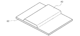
ここで、本実施形態は、図2に示されているように、磁性体グリーンシート上に導電パターン40を印刷した後に上記導電パターン40の厚さの分だけ磁性物質を塗布または印刷することができる。即ち、上記磁性物質は、焼結後、上記磁性体グリーンシートと区別される別途の磁性体層を形成することができる。焼結後、導電パターン40と同一層をなす磁性体層を第1磁性体層64、積層本体15内において上記第1磁性体層64の間に介在する焼結後の上記磁性体グリーンシートは、第2磁性体層62と規定することができる。
In this embodiment, as shown in FIG. 2, after the
上記積層本体15を構成する多数の第1及び第2磁性体層64、62は焼結された状態で、隣接する第1及び第2磁性体層64、62間の境界は、走査電子顕微鏡(SEM、Scanning Eletron Microscope)を使用せずには確認できないほど一体化されていることができる。
The first and second
また、本発明の一実施形態による積層チップインダクタ10のサイズは、外部電極20を含む上記積層本体15の長さ及び幅がそれぞれ2.0±0.1mm及び1.6±0.1mm(2016サイズ)の範囲を有することができ、2016サイズ以下(即ち、積層本体の長さは2.1mm以下で、上記積層本体の幅は1.7mm以下)に形成することもできる。
Further, the size of the
上記第1及び第2磁性体層64、62は、Ni−Cu−Zn系、Ni−Cu−Zn−Mg系、Mn−Zn系のフェライト材料を用いるが、これに限定されるものではない。
The first and second
図2aから図2cを参照すると、フェライトグリーンシート62上に導電パターン40を印刷して乾燥し(図2a)、上記導電パターン40と同一層を形成するように上記導電パターン40の隣の空間にフェライトスラリーをペースト(paste)で印刷して上記フェライトグリーンシート62とは異なる別途の平坦化された磁性体層64を形成する。上記フェライトグリーンシート62、上記導電パターン40と平坦化された磁性体層64が一つの積層キャリア60を形成する(図2b)。また、上記積層キャリア60は、上記導電パターン40が積層方向にコイルパターン50(図4)を形成するように多数が積層されることができる(図2c)。
Referring to FIGS. 2a to 2c, the
このように積層チップインダクタ10を形成すると、導電パターン40と積層キャリア60との間に段差がないため、圧搾または焼結のような工程を経ても導電パターン40が磁性体層60に陥没し、変形される現象が著しく減少する。
When the
図7に示されているように、長さ及び幅方向に研磨して磁性体層60が露出しても、導電パターン40の形状が同一の厚さにおいて導電パターン40の断絶現象がなく、グリーンシートに印刷した導電パターン40の形状をそのまま維持することができる。
As shown in FIG. 7, even if the
上記導電パターン40は、銀(Ag)を主成分とする導電ペーストを所定の厚さで印刷して形成されることができる。上記導電パターン40は、長さ方向の両端部に形成される外部電極20と電気的に連結されることができる。
The
上記外部電極20は、上記セラミック本体15の長さ方向の両端部に形成され、Cu、Ni、Sn、Ag及びPdのうち選択された合金を電気めっきして形成されることができるが、特に、これらの材料に制限されるものではない。
The
上記導電パターン40は、上記外部電極20と電気的に接続されるリードを備えることができる。
The
図3を参照すると、一つの積層キャリア60a上の上記導電パターン40aは、長さ方向の導電パターン42aと、幅方向の導電パターン44aと、を含む。上記導電パターン40aは、磁性体層62aに形成されるビア電極72、74により、磁性体層62aを介して配置される他の一つの積層キャリア60b上の導電パターン40bと電気的に連結され、積層方向にコイルパターン50を形成する。
Referring to FIG. 3, the
本実施形態のコイルパターン50は、全て9.5回のターン数を有するが、これに限定されるものではない。コイルパターン50が9.5回のターン数を有するようにするためには、カバー層をなす上部及び下部の磁性体層80a、80bの間に導電パターン40a、40b、、40mが形成された積層キャリア60a、60b、、60mが13個配置される。
The
本実施形態には、1回のターン数を有するコイルパターン50を形成するため、2個の積層キャリアを必要とする導電パターン42a、44bが開示されているが、これに限定されず、導電パターンの形状によって必要な積層キャリアの数が異なることができる。
In the present embodiment, the
図4を参照して上記コイルパターン50の1回のパターンについて説明すると、同一の磁性体層60bに形成される導電パターン40bにおける一つのビア電極72bを1、他のビア電極74bを2、上記2に対応する積層方向の下部の導電パターン40cにおける一つのビア電極72cを3、上記1に対向する磁性体層60cにおける導電パターン40cの対向地点を4と規定するとき、上記1から反時計回りに1回のターン(1→2→3→4)をなすことを一つのターンと規定することができる。また、上記4を1’と規定するとき、次の1回のターン(1’→2’→3’→4’)が形成されることができる。
Referring to FIG. 4, one pattern of the
図5は、図1のV−V’線に沿った切断面を示す概略図であり、図6は図1のVI−VI’線に沿った切断面を示す概略図である。 5 is a schematic view showing a cut surface along the line V-V ′ of FIG. 1, and FIG. 6 is a schematic view showing a cut surface along the line VI-VI ′ of FIG. 1.
図1の積層チップインダクタを、図5は長さ方向L及び厚さ方向Tに切断し、図6は幅W及び厚さT方向に切断した。 The multilayer chip inductor of FIG. 1 is cut in the length direction L and the thickness direction T in FIG. 5, and in FIG. 6 is cut in the width W and thickness T directions.
図5及び図6の断面図において、導電パターン40が形成されない部分は点線部分で示されている。
In the cross-sectional views of FIGS. 5 and 6, a portion where the
図5に示されているように、長さ方向L及び厚さ方向Tにおいて、導電パターン40が形成される最上部及び最下部の磁性体層には、外部電極20と電気的に連結されるリード48が形成される。上記リード48は、セラミック本体15の長さ方向の短辺Ws1、Ws2に露出し、上記外部電極20と電気的に連結される。
As shown in FIG. 5, the uppermost and lowermost magnetic layers on which the
上記導電パターン40は、第1磁性体層64と同一層をなし、積層本体15内において第2磁性体層62を介して対向配置されることができる。
The
ここで、上記第1磁性体層64は、上記導電パターン40の厚さの分だけ印刷されて形成されることができる。
Here, the first
図7は図1の積層チップインダクタを長さ及び幅方向に研磨して導電パターンが1回のターンを形成する形状を投影して示す概略平面図である。 FIG. 7 is a schematic plan view showing a shape in which the conductive pattern forms one turn by polishing the multilayer chip inductor of FIG. 1 in the length and width directions.
図7を参照すると、導電パターン40が一つのコイルパターン50を形成する詳しい形状が分かる。上記コイルパターン50は、幅方向の導電パターン44及び長さ方向の導電パターン42がビア電極72、74を通じて電気的に接続されて形成される。
Referring to FIG. 7, the detailed shape in which the
ここで、上記長さ方向の導電パターン42において幅方向に形成されるマージン部の幅Wlは、上記幅方向の導電パターン44において長さ方向に形成されるマージン部の幅Llより狭く形成されることができる。これは、図5に示されているように、最上部及び最下部をなす導電パターン40において外部電極20に延長されるリード48の長さを確保するためのものである。
Here, the width Wl of the margin portion formed in the width direction in the
下記表1は、コイルパターンの外部に形成される面積Aoに対するコイルパターンの内部に形成される面積(Ai)の比であるAi/Aoが積層チップインダクタのDC抵抗(Rdc)及びデラミネーション(Delamination)不良に及ぼす影響をチップサイズ別に実験した結果である。 Table 1 below shows that Ai / Ao, which is the ratio of the area (Ai) formed inside the coil pattern to the area Ao formed outside the coil pattern, is the DC resistance (Rdc) and delamination (Delamination) of the multilayer chip inductor. ) This is the result of experimenting the influence on defects according to chip size.
表1のチップは、インダクタンス容量を高めるため、コイルパターンの外部に形成される面積(例えば、図7の「Ao」)をコイルパターンの内部に形成される面積(例えば、図7の「Ai」)より小さく設計した(即ち、Ai/Ao>1)。 In the chip of Table 1, in order to increase the inductance capacity, the area formed outside the coil pattern (for example, “Ao” in FIG. 7) is changed to the area formed in the coil pattern (for example, “Ai” in FIG. 7). ) Designed smaller (ie Ai / Ao> 1).

表1に示されているように、2016サイズを超過するチップの場合、コイルパターンの外部に形成される面積Aoが十分に大きいため、Ai/Ao値が1.03を超過してもDC抵抗(Rdc)が高くなく、デラミネーション(Delamination)不良が発生しなかった。 As shown in Table 1, in the case of a chip exceeding 2016 size, since the area Ao formed outside the coil pattern is sufficiently large, even if the Ai / Ao value exceeds 1.03, the DC resistance (Rdc) was not high, and no delamination defect occurred.
2016サイズ以下のチップにおいてAi/Ao値が1.03を超過する場合は、コイルパターンの外部に形成される面積Aoが相対的に小さいため、小さい電極面積によってDC抵抗(Rdc)が高くなり、デラミネーション(Delamination)不良が発生したことが分かる。 When the Ai / Ao value exceeds 1.03 in a chip of 2016 size or smaller, the area Ao formed outside the coil pattern is relatively small, so that the DC resistance (Rdc) increases due to the small electrode area, It can be seen that a delamination defect has occurred.
従って、2016サイズ以下のチップの場合、十分なインダクタンス容量を確保すると共に、DC抵抗(Rdc)を減らし、デラミネーション(Delamination)不良を防止するためには、本発明の実施形態のようにAi/Ao値を調節する必要がある。 Therefore, in the case of a chip having a size of 2016 or less, in order to secure a sufficient inductance capacity, reduce the DC resistance (Rdc), and prevent a delamination defect, the Ai / It is necessary to adjust the Ao value.
本発明の実施形態において、上記コイルパターン50を上記積層本体15の長さ及び幅方向に投影してみるとき、上記コイルパターンの内部に形成される面積をAi、上記コイルパターンの外部に形成される面積をAoと規定すると、Ai/Aoは、0.40≦Ai/Ao≦1.03の範囲を満たすことができる。
In the embodiment of the present invention, when the
Ai/Aoが0.40未満の場合は、コイルパターン50の内部面積が小さいため、インダクタンス容量を具現することが困難であり、Ai/Aoが1.03超過の場合は、コイルパターン50が長くなるため、DC抵抗(Rdc)が増加して電極が露出することから、デラミネーション(Delamination)不良が発生する可能性がある。
When Ai / Ao is less than 0.40, the internal area of the
また、本発明の他の実施形態によると、上記コイルパターンの面積をAe、上記長さ及び幅方向に投影された上記積層本体の全体面積をAtと規定するとき、Ae/Atは、0.13≦Ae/At≦0.78を満たすことができる。 According to another embodiment of the present invention, when the area of the coil pattern is defined as Ae, and the total area of the multilayer body projected in the length and width directions is defined as At, Ae / At 13 ≦ Ae / At ≦ 0.78 can be satisfied.
Ae/Atが0.13未満の場合は、導電パターン40の断面積が減少するため、DC抵抗(Rdc)が増加し、導電パターン40がなすコイルパターン50が切れてオープン(open)が発生する可能性がある。また、Ae/Atが0.78超過の場合、デラミネーション不良が発生するおそれがある。
When Ae / At is less than 0.13, since the cross-sectional area of the
実験例 Experimental example
本発明の実施例及び比較例による積層チップインダクタは、以下の通り製作された。Ni−Zn−Cu系フェライト粉末を含むスラリーをキャリアフィルム(carrier film)上に塗布及び乾燥して製造された複数個の磁性体グリーンシートを用意する。 Multilayer chip inductors according to examples and comparative examples of the present invention were manufactured as follows. A plurality of magnetic green sheets prepared by applying and drying a slurry containing Ni-Zn-Cu ferrite powder on a carrier film is prepared.
次に、上記磁性体グリーンシート上にスクリーンを用いて銀(Ag)導電性ペーストを塗布し導電パターンを形成する。また、上記導電パターンと同一層になるように上記導電パターンの周りの上記磁性体グリーンシート上にフェライトスラリーを塗布して上記磁性体グリーンシートと共に一つの積層キャリアを形成する。 Next, a silver (Ag) conductive paste is applied on the magnetic green sheet using a screen to form a conductive pattern. Further, a ferrite slurry is applied on the magnetic green sheet around the conductive pattern so as to be in the same layer as the conductive pattern, thereby forming one laminated carrier together with the magnetic green sheet.
導電パターンが形成された積層キャリアを繰り返して積層し、上記導電パターンが電気的に接続されて積層方向にコイルパターンを有するようにする。ここで、上記磁性体グリーンシートには、ビア電極が形成されて上記磁性体グリーンシートを介して上部導電パターン及び下部導電パターンは電気的に接続されることができる。 The laminated carrier on which the conductive pattern is formed is repeatedly laminated so that the conductive pattern is electrically connected to have a coil pattern in the lamination direction. Here, a via electrode is formed on the magnetic green sheet, and the upper conductive pattern and the lower conductive pattern can be electrically connected through the magnetic green sheet.
ここで、上記積層キャリアを10層から20層の範囲内で積層し、この積層体を85℃で1000kgf/cm2の圧力条件で等圧圧縮成形(isostatic pressing)した。圧搾が完了したチップ積層体を個別チップの形態に切断し、切断されたチップは大気雰囲気において230℃で40時間維持して脱バインダーを行った。 Here, the above laminated carrier was laminated in the range of 10 to 20 layers, and this laminated body was isostatic pressing at 85 ° C. under a pressure condition of 1000 kgf / cm 2 . The chip stack after completion of the pressing was cut into individual chips, and the cut chips were debindered by maintaining at 230 ° C. for 40 hours in an air atmosphere.
その後、950℃以下の大気雰囲気において焼成した。このとき、焼成後のチップサイズは、2.0mm×1.6mm(L×W)、2016サイズに製作した。 Then, it baked in the air atmosphere below 950 degreeC. At this time, the chip size after firing was manufactured to 2.0 mm × 1.6 mm (L × W) and 2016 size.
続いて、外部電極の塗布及び電極焼成、めっきなどの工程を経て外部電極を形成した。 Subsequently, external electrodes were formed through steps such as application of external electrodes, electrode firing, and plating.
ここで、上記積層チップインダクタの試料は、一つのコイルパターンを上記積層本体の長さ及び幅方向に投影してみるとき、上記コイルパターンの内部に形成される面積Ai、上記コイルパターンの外部に形成される面積Ao、コイルパターンの面積Ae、上記長さ及び幅方向に投影された上記積層本体の全体面積Atが多様に変更されるように製作された。 Here, in the sample of the multilayer chip inductor, when one coil pattern is projected in the length and width directions of the multilayer body, the area Ai formed inside the coil pattern, outside the coil pattern, The area Ao to be formed, the area Ae of the coil pattern, and the total area At of the multilayer body projected in the length and width directions were manufactured in various ways.
上記Ai、Ao、Ae及びAtは、上記積層本体15の長さ及び幅方向に研磨して得られた切開された断面を光学顕微鏡によって高倍率イメージ撮影し、撮影されたイメージをシグマスキャンプロ(SigmaScan Pro)などのようなコンピュータプログラムで分析して測定した。
Ai, Ao, Ae, and At are obtained by taking a high-magnification image of an incised cross section obtained by polishing the
以下では、本発明の実施例及び比較例の実験データを参照して本発明の実施例についてより具体的に説明する。 Hereinafter, examples of the present invention will be described more specifically with reference to experimental data of examples of the present invention and comparative examples.
下記表2は、長さ及び幅方向の切開された断面におけるAi/Aoによるインダクタンス、DC抵抗及びデラミネーションの発生頻度を測定したものであり、下記表3は、Ai/Ae及びAe/Atによるインダクタンス、DC抵抗及びデラミネーションの発生頻度を測定したものである。 Table 2 below shows the frequency of occurrence of inductance, DC resistance, and delamination due to Ai / Ao in a section cut in the length and width directions, and Table 3 below shows the values according to Ai / Ae and Ae / At. This is a measurement of the frequency of occurrence of inductance, DC resistance and delamination.
インダクタンスは、Agilent 4286A モデルのLCR meterを用いて測定しており、直流抵抗(Rdc)は、Agilent 4338B モデルのmilliohm meterを用いて測定した。 The inductance was measured using an Agilent 4286A model LCR meter, and the direct current resistance (Rdc) was measured using an Agilent 4338B model milliohm meter.
表2を参照すると、Ai/Aoが0.40未満の試料1は、インダクタンス容量が小さく、Ai/Aoが1.03超過の試料9及び10は、DC抵抗(Rdc)が増加する。特に、試料9及び10は、電極露出によるデラミネーション(Delamination)不良が発生した。本発明の実施例である試料2から8は、十分なインダクタンス容量を確保することができ、デラミネーションは発生しない。
Referring to Table 2, Sample 1 with Ai / Ao less than 0.40 has a small inductance capacity, and
表3を参照すると、Ae/Atが増加することにより、上記コイルパターンの内部に形成される面積に対するコイルパターンの面積Ai/Ae及び長さ方向におけるコイルパターンの内部長さに対する外部電極を含む積層チップインダクタの長さ方向の長さFl/Lが減少することが分かる。 Referring to Table 3, as Ae / At increases, the laminate includes the area Ai / Ae of the coil pattern with respect to the area formed inside the coil pattern and the external electrode with respect to the internal length of the coil pattern in the length direction. It can be seen that the length Fl / L in the length direction of the chip inductor decreases.
また、Ae/Atが0.13未満の試料11は、DC抵抗(Rdc)が増加し、回路上オープン(open)が発生した。なお、Ae/Atが0.78超過の試料19は、電極が占める面積が大きすぎてコイルの内部及び外部の面積が非常に減少するようになるため、これにより、容量が低化し、デラミネーション不良が発生した。
Further, in the
10 積層チップインダクタ
20 外部電極
40 導電パターン
60 磁性体層
10
Claims (14)
前記コイルパターンを前記積層本体の長さ及び幅方向に投影してみるとき、前記コイルパターンの内部に形成される面積をAi、前記コイルパターンの外部に形成される面積をAoと規定するとき、
0.40≦Ai/Ao≦1.03を満たし、
前記コイルパターンの面積をAe、前記長さ及び幅方向に投影された前記積層本体の全体面積をAtと規定するとき、
0.13≦Ae/At≦0.78を満たす、積層チップ電子部品。 A multilayer body comprising a large number of magnetic layers that are 2016 size or smaller and on which a conductive pattern is formed, and via electrodes that are electrically connected to form a coil pattern in the stacking direction; Each conductive pattern of the multiple magnetic layers is shorter than the length of one turn of the coil pattern,
When projecting the coil pattern in the length and width directions of the laminated body, when defining the area formed inside the coil pattern as Ai and the area formed outside the coil pattern as Ao,
0.40 ≦ Ai / Ao ≦ 1.03 is satisfied,
When defining the area of the coil pattern as Ae, and the total area of the laminated body projected in the length and width directions as At,
A multilayer chip electronic component satisfying 0.13 ≦ Ae / At ≦ 0.78.
前記長さ方向の導電パターンにおいて幅方向に形成されるマージン部の幅は、前記幅方向の導電パターンにおいて長さ方向に形成されるマージン部の幅より狭い、請求項1に記載の積層チップ電子部品。 The coil pattern includes a conductive pattern in the width direction and a conductive pattern in the length direction,
2. The multilayer chip electron according to claim 1, wherein a width of a margin portion formed in a width direction in the conductive pattern in the length direction is narrower than a width of a margin portion formed in the length direction in the conductive pattern in the width direction. parts.
前記多数の磁性体層の間に配置され、積層方向に電気的に接続されてコイルパターンを形成する導電パターンであって、各前記導電パターンが、前記コイルパターンの1ターンの長さよりも短い、導電パターンと、を含み、
一つの前記コイルパターンを前記積層本体の長さ及び幅方向に投影してみるとき、前記コイルパターンの内部に露出する前記磁性体層の面積をAi、前記コイルパターンの外部に露出する前記磁性体層の面積をAoと規定すると、
0.40≦Ai/Ao≦1.03を満たす、積層チップ電子部品。 A laminated body of 2016 size or less in which a large number of magnetic layers are laminated;
A conductive pattern disposed between the plurality of magnetic layers and electrically connected in a stacking direction to form a coil pattern, wherein each conductive pattern is shorter than a length of one turn of the coil pattern; A conductive pattern,
When projecting one coil pattern in the length and width directions of the laminated body, the area of the magnetic layer exposed inside the coil pattern is Ai, and the magnetic body exposed outside the coil pattern If the area of the layer is defined as Ao,
A multilayer chip electronic component satisfying 0.40 ≦ Ai / Ao ≦ 1.03.
0.13≦Ae/At≦0.78を満たす、請求項8に記載の積層チップ電子部品。 When defining the area of the coil pattern as Ae, and the total area of the laminated body projected in the length and width directions as At,
The multilayer chip electronic component according to claim 8, wherein 0.13 ≦ Ae / At ≦ 0.78 is satisfied.
前記第2磁性体層上に印刷される前記導電パターンの厚さの分だけ磁性物質が塗布されて焼成された第1磁性体層と、を含む、請求項8に記載の積層チップ電子部品。 The magnetic layer includes a second magnetic layer obtained by firing a magnetic green sheet;
The multilayer chip electronic component according to claim 8, further comprising: a first magnetic layer that is coated with a magnetic material by a thickness corresponding to a thickness of the conductive pattern printed on the second magnetic layer and baked.
前記長さ方向の導電パターンにおいて幅方向に形成されるマージン部の幅は、前記幅方向の導電パターンにおいて長さ方向に形成されるマージン部の幅より狭い、請求項8に記載の積層チップ電子部品。 The coil pattern includes a conductive pattern in the width direction and a conductive pattern in the length direction,
The multilayer chip electron according to claim 8, wherein a width of a margin portion formed in a width direction in the conductive pattern in the length direction is narrower than a width of a margin portion formed in the length direction in the conductive pattern in the width direction. parts.
Applications Claiming Priority (2)
| Application Number | Priority Date | Filing Date | Title |
|---|---|---|---|
| KR10-2012-0094540 | 2012-08-28 | ||
| KR1020120094540A KR101771731B1 (en) | 2012-08-28 | 2012-08-28 | Multi-layered chip electronic component |
Publications (2)
| Publication Number | Publication Date |
|---|---|
| JP2014045165A JP2014045165A (en) | 2014-03-13 |
| JP6328370B2 true JP6328370B2 (en) | 2018-05-23 |
Family
ID=50186731
Family Applications (1)
| Application Number | Title | Priority Date | Filing Date |
|---|---|---|---|
| JP2012276525A Active JP6328370B2 (en) | 2012-08-28 | 2012-12-19 | Multilayer chip electronic components |
Country Status (4)
| Country | Link |
|---|---|
| US (1) | US9536647B2 (en) |
| JP (1) | JP6328370B2 (en) |
| KR (1) | KR101771731B1 (en) |
| CN (1) | CN103680815B (en) |
Families Citing this family (9)
| Publication number | Priority date | Publication date | Assignee | Title |
|---|---|---|---|---|
| JP6060116B2 (en) * | 2014-07-18 | 2017-01-11 | 東光株式会社 | Surface mount inductor and manufacturing method thereof |
| CN205656934U (en) * | 2015-10-30 | 2016-10-19 | 线艺公司 | But surface mounting's inductance part |
| US10923259B2 (en) * | 2016-07-07 | 2021-02-16 | Samsung Electro-Mechanics Co., Ltd. | Coil component |
| KR102464309B1 (en) * | 2017-07-04 | 2022-11-08 | 삼성전기주식회사 | Multilayer beads and board for mounting the same |
| KR101994754B1 (en) | 2017-08-23 | 2019-07-01 | 삼성전기주식회사 | Inductor |
| JP6954216B2 (en) * | 2018-04-02 | 2021-10-27 | 株式会社村田製作所 | Laminated coil parts |
| DE102018114785A1 (en) * | 2018-04-13 | 2019-10-17 | Trafag Ag | Method for producing a planar coil arrangement and a sensor head provided therewith |
| JP7169140B2 (en) | 2018-09-27 | 2022-11-10 | 太陽誘電株式会社 | Coil parts and electronic equipment |
| KR102414826B1 (en) * | 2020-06-18 | 2022-06-30 | 삼성전기주식회사 | Coil component |
Family Cites Families (13)
| Publication number | Priority date | Publication date | Assignee | Title |
|---|---|---|---|---|
| JPH1055916A (en) * | 1996-08-08 | 1998-02-24 | Kiyoto Yamazawa | Thin magnetic element and transformer |
| JPH10335143A (en) | 1997-06-04 | 1998-12-18 | Murata Mfg Co Ltd | Laminated inductor |
| JP2001230119A (en) | 2000-02-14 | 2001-08-24 | Murata Mfg Co Ltd | Laminated inductor |
| JP2003017327A (en) * | 2001-06-29 | 2003-01-17 | Fdk Corp | Laminated inductor |
| JP4009142B2 (en) | 2002-06-03 | 2007-11-14 | Fdk株式会社 | Magnetic core type multilayer inductor |
| JP4217438B2 (en) * | 2002-07-26 | 2009-02-04 | Fdk株式会社 | Micro converter |
| JP4417691B2 (en) | 2003-11-07 | 2010-02-17 | 東光株式会社 | Manufacturing method of multilayer electronic component |
| JP4019071B2 (en) * | 2004-07-12 | 2007-12-05 | Tdk株式会社 | Coil parts |
| JP4509186B2 (en) * | 2006-01-31 | 2010-07-21 | 日立金属株式会社 | Laminated component and module using the same |
| JP4895193B2 (en) | 2006-11-24 | 2012-03-14 | Fdk株式会社 | Multilayer inductor |
| CN101889319B (en) | 2007-12-25 | 2013-01-02 | 日立金属株式会社 | Stacked inductor and power converter using the stacked inductor |
| JP2009290121A (en) | 2008-05-30 | 2009-12-10 | Murata Mfg Co Ltd | Method of manufacturing electronic component |
| JP5187858B2 (en) | 2009-01-22 | 2013-04-24 | 日本碍子株式会社 | Multilayer inductor |
-
2012
- 2012-08-28 KR KR1020120094540A patent/KR101771731B1/en active IP Right Grant
- 2012-12-14 US US13/715,899 patent/US9536647B2/en active Active
- 2012-12-19 JP JP2012276525A patent/JP6328370B2/en active Active
-
2013
- 2013-01-09 CN CN201310008006.9A patent/CN103680815B/en not_active Expired - Fee Related
Also Published As
| Publication number | Publication date |
|---|---|
| CN103680815A (en) | 2014-03-26 |
| CN103680815B (en) | 2017-11-10 |
| US9536647B2 (en) | 2017-01-03 |
| US20140062643A1 (en) | 2014-03-06 |
| JP2014045165A (en) | 2014-03-13 |
| KR101771731B1 (en) | 2017-08-25 |
| KR20140028392A (en) | 2014-03-10 |
Similar Documents
| Publication | Publication Date | Title |
|---|---|---|
| JP6328370B2 (en) | Multilayer chip electronic components | |
| TWI733759B (en) | Multilayer inductor | |
| JP5825322B2 (en) | Multilayer ceramic capacitor, method for manufacturing the same, and mounting substrate for multilayer ceramic capacitor | |
| KR102052596B1 (en) | Chip coil component and manufacturing method thereof | |
| US9349512B2 (en) | Multi-layered chip electronic component | |
| JP2020053577A (en) | Electronic component | |
| JP6091838B2 (en) | Multilayer chip electronic components | |
| KR20160004602A (en) | Multi-layered inductor, manufacturing method of the same and board having the same mounted thereon | |
| KR101434103B1 (en) | Multilayered ceramic electronic component and board for mounting the same | |
| JP2007324554A (en) | Laminated inductor | |
| KR20130134868A (en) | Multilayer type inductor | |
| KR20120023689A (en) | Multilayer inductor | |
| JP2015026864A (en) | Multilayer ceramic capacitor | |
| KR101963267B1 (en) | Multi-layered inductor and board for mounting the same | |
| JP2002246267A (en) | Multilayer composite device and its producing method | |
| KR102194723B1 (en) | Chip coil component and manufacturing method thereof | |
| KR20140038782A (en) | Multilayered power inductor and method for preparing the same | |
| KR101933403B1 (en) | Laminated ceramic electronic parts and fabrication method thereof | |
| KR20150006678A (en) | Multilayer inductor and method of manufacturing the same | |
| JP2001244115A (en) | Chip-type composite electronic component and method of manufacturing the same | |
| KR20130134869A (en) | Multilayer type inductor | |
| KR20130104035A (en) | Chip inductor and method of manufacturing the same |
Legal Events
| Date | Code | Title | Description |
|---|---|---|---|
| A621 | Written request for application examination |
Free format text: JAPANESE INTERMEDIATE CODE: A621 Effective date: 20151204 |
|
| A977 | Report on retrieval |
Free format text: JAPANESE INTERMEDIATE CODE: A971007 Effective date: 20161011 |
|
| A131 | Notification of reasons for refusal |
Free format text: JAPANESE INTERMEDIATE CODE: A131 Effective date: 20161025 |
|
| A521 | Request for written amendment filed |
Free format text: JAPANESE INTERMEDIATE CODE: A523 Effective date: 20170106 |
|
| A131 | Notification of reasons for refusal |
Free format text: JAPANESE INTERMEDIATE CODE: A131 Effective date: 20170725 |
|
| A521 | Request for written amendment filed |
Free format text: JAPANESE INTERMEDIATE CODE: A523 Effective date: 20171010 |
|
| TRDD | Decision of grant or rejection written | ||
| A01 | Written decision to grant a patent or to grant a registration (utility model) |
Free format text: JAPANESE INTERMEDIATE CODE: A01 Effective date: 20180327 |
|
| A61 | First payment of annual fees (during grant procedure) |
Free format text: JAPANESE INTERMEDIATE CODE: A61 Effective date: 20180418 |
|
| R150 | Certificate of patent or registration of utility model |
Ref document number: 6328370 Country of ref document: JP Free format text: JAPANESE INTERMEDIATE CODE: R150 |
|
| R250 | Receipt of annual fees |
Free format text: JAPANESE INTERMEDIATE CODE: R250 |
|
| R250 | Receipt of annual fees |
Free format text: JAPANESE INTERMEDIATE CODE: R250 |
|
| R250 | Receipt of annual fees |
Free format text: JAPANESE INTERMEDIATE CODE: R250 |
|
| R250 | Receipt of annual fees |
Free format text: JAPANESE INTERMEDIATE CODE: R250 |