JP6321317B2 - Camera module and OIS (camera shake correction) drive unit - Google Patents
Camera module and OIS (camera shake correction) drive unit Download PDFInfo
- Publication number
- JP6321317B2 JP6321317B2 JP2012179206A JP2012179206A JP6321317B2 JP 6321317 B2 JP6321317 B2 JP 6321317B2 JP 2012179206 A JP2012179206 A JP 2012179206A JP 2012179206 A JP2012179206 A JP 2012179206A JP 6321317 B2 JP6321317 B2 JP 6321317B2
- Authority
- JP
- Japan
- Prior art keywords
- wire spring
- coil
- spring
- wire
- ois
- Prior art date
- Legal status (The legal status is an assumption and is not a legal conclusion. Google has not performed a legal analysis and makes no representation as to the accuracy of the status listed.)
- Active
Links
- 238000012937 correction Methods 0.000 title claims description 14
- 230000035939 shock Effects 0.000 claims description 11
- 230000002093 peripheral effect Effects 0.000 claims description 10
- 230000003287 optical effect Effects 0.000 claims description 8
- 238000005476 soldering Methods 0.000 claims description 8
- 230000003993 interaction Effects 0.000 claims description 7
- 239000007769 metal material Substances 0.000 claims description 5
- 239000006096 absorbing agent Substances 0.000 claims description 4
- 229910000679 solder Inorganic materials 0.000 claims description 3
- 230000001133 acceleration Effects 0.000 claims description 2
- 230000003139 buffering effect Effects 0.000 claims description 2
- 238000000034 method Methods 0.000 description 12
- 239000004020 conductor Substances 0.000 description 6
- 238000013461 design Methods 0.000 description 5
- 238000001514 detection method Methods 0.000 description 5
- 230000008569 process Effects 0.000 description 5
- 239000000853 adhesive Substances 0.000 description 4
- 230000001070 adhesive effect Effects 0.000 description 4
- 239000000463 material Substances 0.000 description 4
- 230000005484 gravity Effects 0.000 description 3
- 239000000758 substrate Substances 0.000 description 3
- 239000004593 Epoxy Substances 0.000 description 2
- 229920005830 Polyurethane Foam Polymers 0.000 description 2
- 230000009471 action Effects 0.000 description 2
- 238000005452 bending Methods 0.000 description 2
- 230000008878 coupling Effects 0.000 description 2
- 238000010168 coupling process Methods 0.000 description 2
- 238000005859 coupling reaction Methods 0.000 description 2
- 238000010586 diagram Methods 0.000 description 2
- 238000012986 modification Methods 0.000 description 2
- 230000004048 modification Effects 0.000 description 2
- 239000011496 polyurethane foam Substances 0.000 description 2
- 230000002265 prevention Effects 0.000 description 2
- 230000006641 stabilisation Effects 0.000 description 2
- 238000011105 stabilization Methods 0.000 description 2
- 238000010521 absorption reaction Methods 0.000 description 1
- 238000013459 approach Methods 0.000 description 1
- 238000006073 displacement reaction Methods 0.000 description 1
- 230000000694 effects Effects 0.000 description 1
- 230000005489 elastic deformation Effects 0.000 description 1
- 229920001971 elastomer Polymers 0.000 description 1
- 238000004519 manufacturing process Methods 0.000 description 1
- 229910052710 silicon Inorganic materials 0.000 description 1
- 239000010703 silicon Substances 0.000 description 1
- 239000007779 soft material Substances 0.000 description 1
- 239000003381 stabilizer Substances 0.000 description 1
Images


Classifications
-
- G—PHYSICS
- G03—PHOTOGRAPHY; CINEMATOGRAPHY; ANALOGOUS TECHNIQUES USING WAVES OTHER THAN OPTICAL WAVES; ELECTROGRAPHY; HOLOGRAPHY
- G03B—APPARATUS OR ARRANGEMENTS FOR TAKING PHOTOGRAPHS OR FOR PROJECTING OR VIEWING THEM; APPARATUS OR ARRANGEMENTS EMPLOYING ANALOGOUS TECHNIQUES USING WAVES OTHER THAN OPTICAL WAVES; ACCESSORIES THEREFOR
- G03B3/00—Focusing arrangements of general interest for cameras, projectors or printers
- G03B3/10—Power-operated focusing
-
- H—ELECTRICITY
- H04—ELECTRIC COMMUNICATION TECHNIQUE
- H04N—PICTORIAL COMMUNICATION, e.g. TELEVISION
- H04N23/00—Cameras or camera modules comprising electronic image sensors; Control thereof
- H04N23/50—Constructional details
- H04N23/54—Mounting of pick-up tubes, electronic image sensors, deviation or focusing coils
-
- G—PHYSICS
- G02—OPTICS
- G02B—OPTICAL ELEMENTS, SYSTEMS OR APPARATUS
- G02B27/00—Optical systems or apparatus not provided for by any of the groups G02B1/00 - G02B26/00, G02B30/00
- G02B27/64—Imaging systems using optical elements for stabilisation of the lateral and angular position of the image
- G02B27/646—Imaging systems using optical elements for stabilisation of the lateral and angular position of the image compensating for small deviations, e.g. due to vibration or shake
-
- G—PHYSICS
- G02—OPTICS
- G02B—OPTICAL ELEMENTS, SYSTEMS OR APPARATUS
- G02B7/00—Mountings, adjusting means, or light-tight connections, for optical elements
- G02B7/02—Mountings, adjusting means, or light-tight connections, for optical elements for lenses
- G02B7/023—Mountings, adjusting means, or light-tight connections, for optical elements for lenses permitting adjustment
-
- G—PHYSICS
- G03—PHOTOGRAPHY; CINEMATOGRAPHY; ANALOGOUS TECHNIQUES USING WAVES OTHER THAN OPTICAL WAVES; ELECTROGRAPHY; HOLOGRAPHY
- G03B—APPARATUS OR ARRANGEMENTS FOR TAKING PHOTOGRAPHS OR FOR PROJECTING OR VIEWING THEM; APPARATUS OR ARRANGEMENTS EMPLOYING ANALOGOUS TECHNIQUES USING WAVES OTHER THAN OPTICAL WAVES; ACCESSORIES THEREFOR
- G03B13/00—Viewfinders; Focusing aids for cameras; Means for focusing for cameras; Autofocus systems for cameras
- G03B13/32—Means for focusing
- G03B13/34—Power focusing
- G03B13/36—Autofocus systems
-
- G—PHYSICS
- G03—PHOTOGRAPHY; CINEMATOGRAPHY; ANALOGOUS TECHNIQUES USING WAVES OTHER THAN OPTICAL WAVES; ELECTROGRAPHY; HOLOGRAPHY
- G03B—APPARATUS OR ARRANGEMENTS FOR TAKING PHOTOGRAPHS OR FOR PROJECTING OR VIEWING THEM; APPARATUS OR ARRANGEMENTS EMPLOYING ANALOGOUS TECHNIQUES USING WAVES OTHER THAN OPTICAL WAVES; ACCESSORIES THEREFOR
- G03B17/00—Details of cameras or camera bodies; Accessories therefor
- G03B17/02—Bodies
-
- G—PHYSICS
- G03—PHOTOGRAPHY; CINEMATOGRAPHY; ANALOGOUS TECHNIQUES USING WAVES OTHER THAN OPTICAL WAVES; ELECTROGRAPHY; HOLOGRAPHY
- G03B—APPARATUS OR ARRANGEMENTS FOR TAKING PHOTOGRAPHS OR FOR PROJECTING OR VIEWING THEM; APPARATUS OR ARRANGEMENTS EMPLOYING ANALOGOUS TECHNIQUES USING WAVES OTHER THAN OPTICAL WAVES; ACCESSORIES THEREFOR
- G03B5/00—Adjustment of optical system relative to image or object surface other than for focusing
-
- H—ELECTRICITY
- H04—ELECTRIC COMMUNICATION TECHNIQUE
- H04N—PICTORIAL COMMUNICATION, e.g. TELEVISION
- H04N23/00—Cameras or camera modules comprising electronic image sensors; Control thereof
- H04N23/50—Constructional details
- H04N23/51—Housings
-
- H—ELECTRICITY
- H04—ELECTRIC COMMUNICATION TECHNIQUE
- H04N—PICTORIAL COMMUNICATION, e.g. TELEVISION
- H04N23/00—Cameras or camera modules comprising electronic image sensors; Control thereof
- H04N23/57—Mechanical or electrical details of cameras or camera modules specially adapted for being embedded in other devices
-
- H—ELECTRICITY
- H04—ELECTRIC COMMUNICATION TECHNIQUE
- H04N—PICTORIAL COMMUNICATION, e.g. TELEVISION
- H04N23/00—Cameras or camera modules comprising electronic image sensors; Control thereof
- H04N23/60—Control of cameras or camera modules
- H04N23/68—Control of cameras or camera modules for stable pick-up of the scene, e.g. compensating for camera body vibrations
- H04N23/681—Motion detection
- H04N23/6812—Motion detection based on additional sensors, e.g. acceleration sensors
-
- H—ELECTRICITY
- H04—ELECTRIC COMMUNICATION TECHNIQUE
- H04N—PICTORIAL COMMUNICATION, e.g. TELEVISION
- H04N23/00—Cameras or camera modules comprising electronic image sensors; Control thereof
- H04N23/60—Control of cameras or camera modules
- H04N23/68—Control of cameras or camera modules for stable pick-up of the scene, e.g. compensating for camera body vibrations
- H04N23/682—Vibration or motion blur correction
- H04N23/685—Vibration or motion blur correction performed by mechanical compensation
- H04N23/687—Vibration or motion blur correction performed by mechanical compensation by shifting the lens or sensor position
-
- G—PHYSICS
- G03—PHOTOGRAPHY; CINEMATOGRAPHY; ANALOGOUS TECHNIQUES USING WAVES OTHER THAN OPTICAL WAVES; ELECTROGRAPHY; HOLOGRAPHY
- G03B—APPARATUS OR ARRANGEMENTS FOR TAKING PHOTOGRAPHS OR FOR PROJECTING OR VIEWING THEM; APPARATUS OR ARRANGEMENTS EMPLOYING ANALOGOUS TECHNIQUES USING WAVES OTHER THAN OPTICAL WAVES; ACCESSORIES THEREFOR
- G03B2205/00—Adjustment of optical system relative to image or object surface other than for focusing
- G03B2205/0007—Movement of one or more optical elements for control of motion blur
- G03B2205/0015—Movement of one or more optical elements for control of motion blur by displacing one or more optical elements normal to the optical axis
-
- G—PHYSICS
- G03—PHOTOGRAPHY; CINEMATOGRAPHY; ANALOGOUS TECHNIQUES USING WAVES OTHER THAN OPTICAL WAVES; ELECTROGRAPHY; HOLOGRAPHY
- G03B—APPARATUS OR ARRANGEMENTS FOR TAKING PHOTOGRAPHS OR FOR PROJECTING OR VIEWING THEM; APPARATUS OR ARRANGEMENTS EMPLOYING ANALOGOUS TECHNIQUES USING WAVES OTHER THAN OPTICAL WAVES; ACCESSORIES THEREFOR
- G03B2205/00—Adjustment of optical system relative to image or object surface other than for focusing
- G03B2205/0053—Driving means for the movement of one or more optical element
- G03B2205/0069—Driving means for the movement of one or more optical element using electromagnetic actuators, e.g. voice coils
Description
本発明は、カメラモジュール及びOIS(手振れ補正)駆動ユニットに関するものである。 The present invention relates to a camera module and an OIS (camera shake correction) drive unit .
小型の電子製品に実装されるカメラモジュールは、使用中に頻繁に衝撃を受けたり、撮影時に使用者の手振れなどによって微細に揺れることがある。そこで、最近では、手振れ防止手段を有するカメラモジュールが開示されている。 A camera module mounted on a small electronic product may be frequently shocked during use or may be shaken minutely due to a user's hand shake during photographing. Therefore, recently, a camera module having a camera shake preventing means has been disclosed.
例えば、韓国登録特許第10−0741823号(2007年07月16日登録)では、手振れ現象を補正するために、ジャイロ(Gyro)センサーICまたは角速度センサーを、携帯電話のようなカメラモジュール付き装置の内部に取り付ける方法が紹介されている。 For example, in Korean Registered Patent No. 10-0741823 (registered on July 16, 2007), a gyro sensor IC or an angular velocity sensor is installed in a device with a camera module such as a mobile phone in order to correct a camera shake phenomenon. How to install inside is introduced.
しかしながら、このように別途の角速度検出センサーを備えると、手振れ防止機能を具現するために別途の感知センサーを備えなければならず、製造コストの上昇につながるだけでなく、カメラモジュールとは別途に手振れ防止装置を構成及び設置するための空間を備えなければならず、面倒である。 However, if a separate angular velocity detection sensor is provided in this way, a separate detection sensor must be provided in order to implement a camera shake prevention function, which not only leads to an increase in manufacturing cost but also a camera shake separately from the camera module. A space for configuring and installing the prevention device must be provided, which is cumbersome.
本発明の目的は、手振れ補正(Optical Image Stabilizer)機能を有するカメラモジュールを提供することにある。 SUMMARY OF THE INVENTION An object of the present invention is to provide a camera module having a function of correcting camera shake (Optical Image Stabilizer).
本発明に係るカメラモジュールは、イメージセンサーが実装される第1印刷回路基板と、前記第1印刷回路基板の上側に配置されるハウジングユニットと、前記ハウジングユニットの内部底面から一定距離離隔して配置され、外周面に第1コイルが巻線され、内部に少なくとも1枚のレンズを含むホルダーモジュールと、前記ホルダーモジュールの底面に結合される第2印刷回路基板と、前記ホルダーモジュールの上側に設けられる第3印刷回路基板と、一端は、前記第2印刷回路基板と連結され、他端は、前記第3印刷回路基板と連結される複数個のワイヤースプリングと、前記ワイヤースプリングと前記第3印刷回路基板との連結部分に前記ワイヤースプリングと一体に形成された緩衝部と、を含むことを特徴とする。 A camera module according to the present invention includes a first printed circuit board on which an image sensor is mounted, a housing unit disposed on an upper side of the first printed circuit board, and a predetermined distance from an inner bottom surface of the housing unit. A holder module including a first coil wound on an outer peripheral surface and including at least one lens therein; a second printed circuit board coupled to a bottom surface of the holder module; and a top side of the holder module. The third printed circuit board has one end connected to the second printed circuit board and the other end connected to the third printed circuit board, a plurality of wire springs, the wire spring, and the third printed circuit. A buffer portion integrally formed with the wire spring is included in a connection portion with the substrate.
前記緩衝部は、前記ワイヤースプリングをジグザグ状に折り曲げて形成されてもよく、前記ワイヤースプリングをコイルスプリング状にバンディングして形成されてもよい。 The buffer portion may be formed by bending the wire spring in a zigzag shape, or may be formed by banding the wire spring in a coil spring shape.
前記ハウジングユニットは、前記第1印刷回路基板の上側に配置される第1ハウジングと、前記第1ハウジングの上側に配置され、上側に前記第3印刷回路基板が設けられる第2ハウジングと、前記第1及び第2ハウジングの間に介在される第1及び第2永久磁石と、前記第1及び第2永久磁石の間に配置され、前記ホルダーモジュールの内部に磁気力を伝達するヨークと、を備えることが好ましい。 The housing unit includes a first housing disposed on the upper side of the first printed circuit board, a second housing disposed on the upper side of the first housing, and provided with the third printed circuit board on the upper side, First and second permanent magnets interposed between the first and second housings, and a yoke disposed between the first and second permanent magnets and transmitting magnetic force to the inside of the holder module. It is preferable.
前記ハウジングユニットは、前記第1印刷回路基板の上側に配置される第1ハウジングと、前記第1ハウジングの上側に配置され、上側に前記第3印刷回路基板が設けられる第2ハウジングと、前記第1及び第2ハウジングの内側面に配置される第1及び第2永久磁石と、前記第1及び第2永久磁石の間に配置され、前記ホルダーモジュールの内部に磁気力を伝達するヨークと、を備えることが好ましい。 The housing unit includes a first housing disposed on the upper side of the first printed circuit board, a second housing disposed on the upper side of the first housing, and provided with the third printed circuit board on the upper side, First and second permanent magnets disposed on the inner surface of the first and second housings, and a yoke disposed between the first and second permanent magnets and transmitting magnetic force to the inside of the holder module. It is preferable to provide.
本発明の好適な一実施例によれば、前記カメラモジュールは、前記第3印刷回路基板とワイヤースプリングとの連結部及びレンズモジュールに対応する位置に貫通孔を有し、前記ハウジングユニットを取り囲むように設けられるシールド缶をさらに含むことができる。 According to a preferred embodiment of the present invention, the camera module has a through hole at a position corresponding to the connecting portion of the third printed circuit board and the wire spring and the lens module so as to surround the housing unit. Further, a shield can provided on the can.
前記ホルダーモジュールは、外周面に第1コイルが巻線されるアウターブレード(outer blade)と、前記アウターブレードの上側に弾性部材により弾持され、前記アウターブレードの内側で上下移動可能に配置され、その外周面に第2コイルが巻線され、その内部には少なくとも1枚のレンズが設けられるボビンと、前記ボビンの上側及び下側にそれぞれ配置され、前記ボビンを前記アウターブレードに対して弾持する上側及び下側弾性部材と、を備え、前記第1コイルの中央は、前記第2コイル側に磁気力が透磁されるように空間部が形成されることが好ましい。 The holder module has an outer blade around which a first coil is wound on an outer peripheral surface, and is elastically supported on the upper side of the outer blade by an elastic member, and is arranged to be movable up and down inside the outer blade. A second coil is wound on the outer peripheral surface, and a bobbin provided with at least one lens inside thereof is disposed on the upper side and the lower side of the bobbin, respectively, and the bobbin is held against the outer blade. It is preferable that a space portion is formed in the center of the first coil so that a magnetic force is transmitted to the second coil side.
前記ヨークは、前記ホルダーモジュールに向かう中央付近が突出形成されると好ましい。 The yoke is preferably formed so as to protrude near the center toward the holder module.
前記ホルダーモジュールは、外周面に第1コイルが巻線されるアウターブレードと、前記アウターブレードの上側に弾性部材により弾持され、前記アウターブレードの内側で上下移動可能に配置され、その外周面に第2コイルが巻線され、その内部には少なくとも1枚のレンズが設けられるボビンと、前記ボビンの上側及び下側にそれぞれ配置され、前記ボビンを前記アウターブレードに対して弾持する上側及び下側の弾性部材と、を備えることが好ましい。 The holder module has an outer blade around which a first coil is wound on an outer peripheral surface, is elastically supported by an elastic member on the upper side of the outer blade, and is arranged so as to be vertically movable inside the outer blade. A bobbin around which a second coil is wound and at least one lens is provided, and an upper side and a lower side that are respectively arranged on the upper side and the lower side of the bobbin and hold the bobbin against the outer blade. It is preferable to provide a side elastic member.
前記第2印刷回路基板は、前記アウターブレードの底面に設けられるとよい。 The second printed circuit board may be provided on a bottom surface of the outer blade.
前記第2印刷回路基板は、前記アウターブレードの底面に接着部材で固定されることが好ましい。 The second printed circuit board is preferably fixed to the bottom surface of the outer blade with an adhesive member.
前記ワイヤースプリングは、金属材質で形成され、前記第2及び第3印刷回路基板と通電可能に連結されるとよい。 The wire spring may be formed of a metal material and connected to the second and third printed circuit boards so as to be energized.
また、前記ワイヤースプリングは、少なくとも6個が設けられ、オットーフォーカシング制御のための2個の極性とOIS駆動のための4個の極性電源を、前記第2及び第3印刷回路基板との連結を通じて前記ホルダーモジュールに供給することが好ましい。 Further, at least six wire springs are provided, and two polar power sources for Otto focusing control and four polar power sources for OIS driving are connected to the second and third printed circuit boards. It is preferable to supply the holder module.
また、前記ワイヤースプリングは、同一の長さを有し、前記ホルダーモジュールの隅部に2個ずつ配置されて総8個が設けられるとよい。 In addition, the wire springs may have the same length, and two wire springs may be provided at the corners of the holder module to provide a total of eight.
ここで、前記第2コイルは、前記下側スプリングに通電可能に連結され、前記下側スプリングは、前記第2印刷回路基板で前記ワイヤースプリングと通電可能に連結されることが好ましい。 Here, it is preferable that the second coil is connected to the lower spring so as to be energized, and the lower spring is connected to the wire spring so as to be energized on the second printed circuit board.
前記第2コイルは、前記第2印刷回路基板と直接通電可能に連結されるとよい。 The second coil may be connected to the second printed circuit board so as to be directly energized.
前記第1コイルの中央は、前記第2コイル側に磁気力が透磁されるように空間部が形成されるとよい。 A space may be formed at the center of the first coil so that a magnetic force is transmitted to the second coil side.
本発明によれば、反復的に加えられる荷重を吸収できるようにワイヤースプリングに緩衝部を有するので、印刷回路基板の連結部に強固に連結することが可能になる。 According to the present invention, since the wire spring has the buffer portion so as to absorb the repeatedly applied load, it can be firmly connected to the connection portion of the printed circuit board.
また、ワイヤースプリングがレンズモジュールの組立工程中に過度な力を受けても、過度に加えられた力を緩衝部材で吸収できるため、組立性が向上する他、組立不良による部品損失も最小化することができる。 Even if the wire spring receives an excessive force during the assembly process of the lens module, the excessive force can be absorbed by the buffer member, so that the assemblability is improved and the component loss due to the assembly failure is minimized. be able to.
以下、本発明の好適な実施例を、図面を参照して説明する。 Hereinafter, preferred embodiments of the present invention will be described with reference to the drawings.
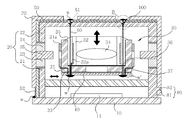
図1は、本発明の一実施例に係るカメラモジュールの概略的な平面図、図2は、図1のA−A断面図、図3は、本発明の一実施例に係るカメラモジュールの側面図、図4は、図3のシールド缶を除去した状態を示す側面図、図5は、本発明の第1実施例に係る図2のB部分を拡大して示す図、そして、図6は、本発明の第2実施例に係る図2のB部分を拡大して示す図である。 1 is a schematic plan view of a camera module according to an embodiment of the present invention, FIG. 2 is a cross-sectional view taken along line AA of FIG. 1, and FIG. 3 is a side view of the camera module according to an embodiment of the present invention. 4 is a side view showing a state where the shield can of FIG. 3 is removed, FIG. 5 is an enlarged view showing a portion B of FIG. 2 according to the first embodiment of the present invention, and FIG. FIG. 5 is an enlarged view showing a portion B of FIG. 2 according to the second embodiment of the present invention.
図1の概略的な平面図、及び図1のA−A断面を示す概略的な側面図である図2に示すように、本発明に係るカメラモジュールは、第1印刷回路基板10、ハウジングユニット20、ホルダーモジュール30、第2印刷回路基板40、第3印刷回路基板50、ワイヤースプリング60、及び緩衝部100を含む。
As shown in FIG. 2 which is a schematic plan view of FIG. 1 and a schematic side view showing a cross section AA of FIG. 1, the camera module according to the present invention includes a first printed
第1印刷回路基板10は、略中央付近にイメージセンサー11が実装され、PCB基板からなることが好ましい。第1印刷回路基板10には、イメージセンサー11の作動のための構成要素を配置したり、電源の供給及びイメージセンサー11の情報の出力を可能にする複数の端子部を設けたりすることができる。
The first printed
ハウジングユニット20は、第1印刷回路基板10の上側に配置されるもので、カメラモジュールの骨格を形成する。本発明の好ましい一実施例によれば、ハウジングユニット20は、第1ハウジング21、第2ハウジング22、第1及び第2永久磁石23,24、及びヨーク25を含む。
The
第1ハウジング21はベースであり、第1印刷回路基板10の上側面に配置され、イメージセンサー11と一定の距離をおいて設けられる。第1ハウジング21には、必要によって、イメージセンサー11に入射するイメージ像をろ過できるフィルター部材をさらに設けられてもよい。
The
第2ハウジング22は、第1ハウジング21の上側に配置され、第1ハウジング21を覆うように構成される。第2ハウジング22の概略中央付近には、イメージセンサー11側に画像が伝達されるように、対応する位置に開口部が形成される。第2ハウジング22の上側面には、後述される第3印刷回路基板50が両面テープや接着剤のような固定部材により固着されるが、これに限定されるものではなく、製品設計によって、ケースやシールド缶のような別途の第3ハウジングを備え、その内側面に第3印刷回路基板50を上記の固定部材で固定することも可能である。第3ハウジングが設けられる場合は、別の固定部材無しで、第3ハウジングで第3印刷回路基板50を押して支持することも可能である。
The
第1及び第2永久磁石23,24は、第1及び第2ハウジング21,22で挟持され、磁気力をホルダーモジュール30に透磁する。第1及び第2永久磁石23,24は、同じ大きさにするとよい。また、第1及び第2永久磁石23,24及びヨーク25は、設計許容値範囲内で、可能であれば、第1及び第2ハウジングの内側面に配置されてもよい。
The first and second
一方、第1及び第2永久磁石23,24の大きさが増大すると、小さい電流でもOIS駆動が大きくなり、万一、第1及び第2永久磁石23,24の大きさを一定に構成する場合は、第1及び第2永久磁石23,24に対応する位置に配置される第1及び第2コイル31a,32aに流れる電流を増大させるほど、OIS駆動が大きくなる。要するに、第1及び第2永久磁石23,24の大きさが大きいほどOIS駆動はよくなるが、その他の設計許容値を考慮してその最適大きさを設計することが好ましい。
On the other hand, when the size of the first and second
ヨーク25は、第1及び第2永久磁石23,24の間に挟持される。また、ヨーク25は、第1及び第2永久磁石23,24の磁気力をホルダーモジュール30の内部空間に透磁できるように、中央付近が突出した形状とする。好ましくは、ヨーク25を、第1及び第2永久磁石23,24と同一の幅を有し、中央が一定大きさで突出する形状にすることで、永久磁石とヨークとを概略“T”字状にするとよい。
The
ホルダーモジュール30は、ハウジングユニット20の内部底面から一定距離離隔して配置されるもので、アウタブレード31とボビン32とで構成される。ホルダーモジュール30は、ワイヤースプリング60にぶら下がっている状態で前後/左右及び対角線方向に振り子運動ができる。
The
アウタブレード31は、上側及び下側にスプリング部材35,36が設けられ、このスプリング部材35により弾持されて、ボビン32の上下運動が可能なように連結されている。
The
アウタブレード31は、図1に示すように、4側面の外周面に総4個の第1コイル31a〜31dが巻線されており、これらコイル31a〜31dの巻かれている4側面の中央部は、コイル無しで開いている。この開いている空間部と対応する位置にはヨーク25が配置され、ヨーク25がこの空間部の内側に一部挿入される構成にしてもよい。
As shown in FIG. 1, the
アウタブレード31の底面には、第2印刷回路基板40を両面テープや接着剤のような固定部材33で固定することができる。アウタブレード31は第1及び第2永久磁石23,24の磁気力と第1コイル31aとの相互作用によって、図2の矢印で示すように、前後左右または対角線に移動できるように複数個のワイヤースプリング60にぶら下がり、第1ハウジング21の底面から所定間隔離隔して配置される。
The second printed
また、アウタブレード31には、ワイヤースプリング60が貫通して第2印刷回路基板40と連結されるように複数個のスプリング通孔37を設けることができる。
Further, the
ボビン32は、アウタブレード31の内側に上下移動可能に配置され、その内部には少なくとも1枚のレンズ34が取り付けられる。ボビン32の外周面には第2コイル32aが巻線されるが、第2コイル32aは、ヨーク25から、アウタブレード31の第1コイル31a〜31dが設けられていない開いている空間を通して透磁された磁気力との相互作用により、ボビン32を上昇及び下降させる動作を行う。ヨーク25の大きさが増大するほどAF駆動はよくなるが、これも最適設計値に従えばよい。このようなボビン32の昇降作用により、イメージセンサー11に伝達されるイメージの焦点を自動で調節することが可能になる。
The
第2印刷回路基板40は、上述したように、アウタブレード31の底面に配置され、第1及び第2コイル31a,32aに電源を供給できるようにワイヤースプリング60が連結される。連結方式は、ソルダリングやその他導電物質で連結されるものであれば、いずれの方式も可能である。すなわち、第2印刷回路基板40の連結部w’は、図2に示すように、第1及び第2コイル31a,32aとそれぞれ連結され、ワイヤースプリング60を通して供給された電源を第1及び第2コイル31a,32aに伝達し、電磁気力を形成できるようにする。
As described above, the second printed
この時、第2コイル32aは、第2印刷回路基板40と直接連結されてもよく、図2に示すように、まず下側スプリング36に連結された後、この下側スプリング36が第2印刷回路基板40と連結されるようにしてもよい。
At this time, the
第3印刷回路基板50は、第2ハウジング22の上側に、上述したように、両面テープ、接着部材のような固定部材で固定されるが、第1印刷回路基板10と連結されている第3印刷回路基板50の端子部52を通して伝達された電源は、第2印刷回路基板40と共に連結されたワイヤースプリング60を通して第2印刷回路基板40に伝達する。連結方式は、ソルダリングやその他導電物質で連結されるものであれば、いずれの方式も可能である。
As described above, the third printed
第3印刷回路基板50は、図3及び図4に示すように、第1及び第2ハウジング21,22の一側壁面を覆うように設けられるが、第1及び第2永久磁石23,24とヨーク25に相対する面にはウィンドウ55が形成され、それらとの干渉を回避できるような構成とすることができる。
As shown in FIGS. 3 and 4, the third printed
これは、第1及び第2永久磁石23,24とヨーク25は、主に、後述するシールド缶70にエポキシのような固定手段で直接付着されるためである。
This is because the first and second
一方、第2印刷回路基板40及び第3印刷回路基板50としては、フレキシブル印刷回路基板(FPCB)、印刷回路基板(PCB)またはR−FPCB(Rigid FPCB一体型)が可能であるが、これに限定されるものではなく、電気的に連結可能にする基板であれば、いずれも使用可能である。
On the other hand, the second printed
ワイヤースプリング60は、両端が第2及び第3印刷回路基板40,50に連結される。この時、ワイヤースプリング60の一端は、図5に示すように、第3印刷回路基板50に形成されたパッド51において連結され、パッド51の中央にはワイヤースプリング60が貫通する通孔53が形成される。連結方式は、ソルダリングやその他導電物質で連結されるものであれば、いずれの方式も可能である。一方、パッド51の周辺は、ソルダーレジスタ(SR、solder register)が設けられて、第3印刷回路基板50の表面を保護し、パッド51領域は、ソルダーレジスタをオープンさせて通電可能に連結することができる。
The
このように、パッド51において連結されたワイヤースプリング60は、端子部52から供給された電源を第2印刷回路基板40側に供給し、第1及び第2コイル31a,32aが第1及び第2永久磁石23,24と相互作用できるようにする。
As described above, the
また、ワイヤースプリング60の他端は、図2に示すように、アウタブレード31に形成されたスプリング通孔37を通過して、アウタブレード31の底面に設けられている第2印刷回路基板40に連結される。この時、ワイヤースプリング60の他端は、図示してはいないが、第3印刷回路基板50と同様、第2印刷回路基板40に形成されているパッド(図示せず)において連結されるが、パッド(図示せず)の中央にはワイヤースプリング60が貫通する通孔(図示せず)が形成される。連結方式は、ソルダリングやその他導電物質で連結されるものであれば、いずれの方式も可能である。このような構成によれば、アウタブレード31はワイヤースプリング60につり下がって第1ハウジング21の底面と一定距離以上離隔することができる。そのため、第1コイル31aと第1及び第2永久磁石23,24との相互作用によって、アウタブレード31が振り子運動を行い、手振れによりアウタブレード31が振動することを、第1コイル31aと第1及び第2永久磁石23,24との相互作用により補正することが可能になる。そのために、ワイヤースプリング60は衝撃に耐えられるように弾性を有し、通電可能な金属材質からなることが好ましい。
Further, as shown in FIG. 2, the other end of the
一方、ワイヤースプリング60の太さが小さいほど、小さい電流に対しても効率よく手振れ補正運動ができるが、これは最適設計値に従えばよい。好ましくは、ワイヤースプリング60の太さは、数μmから数百μm、好ましくは、1乃至100μmを有するとよい。
On the other hand, the smaller the thickness of the
また、ワイヤースプリング60は、少なくとも6個設けられることが好ましい。少なくともオートフォーカシング制御のための2個の極性と手振れ補正のための4個の極性電源を、第2及び第3印刷回路基板40,50との連結を通じてホルダーモジュール30に供給する必要があるためである。
Moreover, it is preferable that at least six wire springs 60 are provided. This is because at least two polarities for auto-focusing control and four polar power sources for camera shake correction need to be supplied to the
本発明の好適な一実施例によれば、図1及び図2に示すように、ワイヤースプリング60は、同一長さでホルダーモジュール30の隅部にそれぞれ2個ずつ配置し、総8個を設けてバランスをとることができる。
According to a preferred embodiment of the present invention, as shown in FIGS. 1 and 2, two wire springs 60 are arranged at the corner of the
一方、図2に示すように、シールド缶70のような別途の第3ハウジングをさらに含む場合に、上述したように、第3印刷回路基板50は、第1及び第2永久磁石23,24とヨーク25がシールド缶70にエポキシなどで結合されるため、この結合部分を回避するために、ウィンドウ55を形成して第1及び第2ハウジング21,22の側壁面を覆う。
On the other hand, as shown in FIG. 2, when the third printed
もし、シールド缶70が省かれる構成では、第3印刷回路基板50をPCBなどで形成し、その内部に第1及び第2永久磁石23,24とヨーク25を付着して固定することも可能であり、上述したように、第3印刷回路基板50をPCBで構成すると共に、前述のウィンドウ55を設けて、該ウィンドウ55に第1及び第2永久磁石23,24とヨーク25を挿入し、その外部にシールドテープなどでさらに補強して構成することも可能である。
If the shield can 70 is omitted, the third printed
緩衝部100は、ワイヤースプリング60の一部区間に一体に形成されることが好ましい。緩衝部100は、図5に示すように、ワイヤースプリング60をジグザグ状に折り曲げて形成してもよく、図6に示すように、コイルスプリング状にバンディングして形成してもよい。
The
この場合、緩衝部100は、ワイヤースプリング60が第2ハウジング22と干渉しない位置で第2ハウジング22の形状に応じて設計することができる。
In this case, the
緩衝部100は、上広下狭の構造を有し、図5及び図6に示すように、下側へ行くほど狭くなる円錘形の漏斗状にすることが好ましい。支持孔122は、通孔53と同軸上に貫通形成され、通孔53と同一または大きい径とすることが好ましい。
The
通孔53の径は、ワイヤースプリング60の径よりもやや大きく形成されるとよく、ワイヤースプリング60が第3印刷回路基板50に形成されているパッド51において連結される時に、ソルダリングやその他の導電物質のような連結物質が、通孔53に沿って流れて第3印刷回路基板50の上下面の両面でワイヤースプリング60と連結されて固定されるように設計することができる。
The diameter of the through
また、支持孔122の径は、ワイヤースプリング60の径よりもやや大きく形成されるとよく、通孔53と同一径または大径に形成されてもよい。すなわち、ワイヤースプリング60が支持孔122付近の第2ホルダー22に接触して干渉が起きることを防ぐように設計すればよい。
The diameter of the
このように構成された緩衝部100は、ワイヤースプリング60に付加される荷重を吸収する役割を果たすから、第3印刷回路基板50に設けられたパッド51に付加される荷重を軽減し、ワイヤースプリング60を固定している連結部wに直接的に付加される荷重を軽減することができる。
Since the
一方、一般の組立順序は、ボビン32とアウタブレード31とを結合した後に、ジグを用いて、第2ハウジング22、第2及び第3印刷回路基板40,50とワイヤースプリング60とを連結し、レンズバレルの設けられているボビン32を結合した後に、第1ハウジング21を連結し、これを第1印刷回路基板10にマウントする。第1ハウジング21を連結する前に永久磁石、ヨークの結合が行われてもよい。この組立順序は必要に応じて変更してもよい。すなわち、ジグ無しで装備で直接組み立てることも可能である。この過程においてレンズバレルの設けられているボビン32を挿入結合する力が大きすぎて連結部wに無理を与えても、この過度な力を緩衝部100で吸収することができる。
On the other hand, the general assembly sequence is to connect the
すなわち、緩衝部100は、図2、図5及び図6に示すように、ワイヤースプリング60及び第3印刷回路基板50の連結部wの付近において、ワイヤースプリング60に荷重が発生して重力方向に引っ張られたり、左右に揺れたりする場合に発生する荷重を、緩衝部100の変形エネルギーとして吸収する。
That is, as shown in FIGS. 2, 5, and 6, the
そのため、組立工程中に連結部wの破損により再び連結作業を行ったり、部品が使用できなくなるといった不具合を防止でき、より高信頼性のカメラモジュールを生産することが可能である。 Therefore, it is possible to prevent problems such as connecting work again due to breakage of the connecting part w during the assembling process, or inability to use parts, and it is possible to produce a more reliable camera module.
一方、本発明の第2実施例によれば、図7及び図8に示すように、緩衝部100に代えて緩衝部材1100をさらに備えることも可能である。
On the other hand, according to the second embodiment of the present invention, as shown in FIGS. 7 and 8, it is possible to further include a
緩衝部材1100は、図7に示すように、第2ハウジング22と第3印刷回路基板50との間に挟まれるもので、ワイヤースプリング60と第3印刷回路基板50との連結のために第3印刷回路基板50に設けられたパッド51またはワイヤースプリング60で発生する力を吸収し、連結部wに働く荷重を分散吸収する役割を果たす。
As shown in FIG. 7, the
通孔53の径は、ワイヤースプリング60の径よりもやや大きく形成されるとよく、ワイヤースプリング60が第3印刷回路基板50に形成されているパッド51において連結される時に、ソルダリングやその他の導電物質のような連結物質が、通孔53に沿って流れて第3印刷回路基板50の上下面の両面でワイヤースプリング60と連結されて固定されるように設計することができる。
The diameter of the through
また、支持孔122の径は、ワイヤースプリング60の径よりもやや大きく形成されるとよく、通孔53よりも大径に形成されて、ワイヤースプリング60が支持孔122付近の第2ホルダー22に接触して干渉が起きることを防ぐように設計すればよい。
The diameter of the
本発明の好適な第3実施例によれば、緩衝部材1100は、第2ハウジング22の上端部の第3印刷回路基板50に相対する面全体に配置されることが好ましく、図示してはいないが、連結部w周辺にのみ配置されてもよい。
According to a third preferred embodiment of the present invention, the
緩衝部材1100は、耐衝撃性部材であるマイクロセルラーポリウレタンフォーム(microcellular polyurethane foam)で形成することができる。このようなマイクロセルラーポリウレタンフォームの一例にポロン(PORON)などを用いることができるが、これを限定されるものではなく、外部力により弾性変形可能な材質であれば、いずれも使用可能である。
The
緩衝部材1100は、パッド51と通孔53のそれぞれの末端から一定距離離隔して配置することで、第3印刷回路基板50が破れることを防止することができる。図5に示すように、緩衝部材1100は、通孔53の末端とパッド51の末端との間に配置され、第3印刷回路基板50及び第2ハウジング22を固定することができ、ワイヤースプリング60を固定している連結部wに直接的に付加される荷重を軽減することができる。
The
また、緩衝部材1100は、支持孔122の末端、または支持孔122末端から一定距離離隔した位置(図示せず)において第3印刷回路基板50と第2ハウジング22との間に配置され、緩衝の役割を果たすこともできる。
The
すなわち、緩衝部材1100は、図7及び図8に示すように、パッド51と面接触可能に配置されるので、ワイヤースプリング60に荷重が発生して重力方向に引っ張られたり、左右に揺れたりする時に発生する荷重は、まずパッド51に加えられ、続いて緩衝部材1100に伝達されて弾性変形されるため、荷重エネルギーは緩衝部材1100の変形エネルギーとして吸収される。
That is, as shown in FIGS. 7 and 8, the
そのため、組立工程中に連結部wの破損により連結作業を再び行ったり、部品が使用できなくなるといった不具合を防止することができる。 For this reason, it is possible to prevent problems such as performing the connecting operation again due to breakage of the connecting portion w during the assembling process or making the parts unusable.
一方、本発明の第4乃至第6実施例によれば、ワイヤースプリング60に緩衝部2100を形成することも可能である。
On the other hand, according to the fourth to sixth embodiments of the present invention, the
すなわち、緩衝部2100は、ワイヤースプリング60の一部区間に一体に形成されることが好ましい。本発明の好適な第4実施例によれば、緩衝部2100は、図9及び図10に示すように、ワイヤースプリング60と第3印刷回路基板50の連結部w、及びワイヤースプリング60と第2印刷回路基板40の連結部w’の近くに形成されることが好ましい。
That is, the
ここで、緩衝部2100は、ワイヤースプリング60の第2ハウジング22と干渉しない位置で第1及び第2折り曲げ部2110,2120を持つように形成されることが好ましいが、これを限定するものではなく、必要によって2回以上折り曲げ、折り曲げられた地点でワイヤースプリング60に付加される荷重を吸収できるようにしてもよい。
Here, the
すなわち、図10に示すように、第1及び第2折り曲げ部2110,2120は、ワイヤースプリング60に付加される荷重に従って、折り曲げられたワイヤースプリング60のモーメント中心になりながら、折り曲げられたワイヤースプリング60が一直線になる方向に変形可能である。そのため、それぞれの第1及び第2折り曲げ部2110,2120を中心に変形が、ワイヤースプリング60に付加される荷重を吸収する役割を担うので、第3印刷回路基板50に設けられたパッド51に付加される荷重を軽減し、ワイヤースプリング60を固定している連結部wに直接的に付加される荷重を軽減することができる。
That is, as shown in FIG. 10, the first and second
本発明の好適な第5実施例によれば、緩衝部2100は、図11に示すように、ワイヤースプリング60と第3印刷回路基板50との連結部wの近くにのみ形成されてもよい。すなわち、ワイヤースプリング60と第3印刷回路基板50との連結部wは、ホルダーモジュール30をぶら下げているワイヤースプリング60の荷重が集中してかかる位置であるから、アウターブレード31の底面に設けられた第2印刷回路基板40と連結される連結部w'に比べて相対的に大きい力がかかる。そのため、ワイヤースプリング60と第3印刷回路基板50との連結部wに近い位置にのみ緩衝部2100を備えてもよい。
According to the fifth preferred embodiment of the present invention, the
また、本発明の好適な第6実施例によれば、緩衝部2100は、図12に示すように、ワイヤースプリング60と第2印刷回路基板40のと連結部w’の付近にのみ形成されてもよい。もちろん、第2実施例で説明したように、集中して荷重のかかる位置は、ワイヤースプリング60と第3印刷回路基板50との連結部wであるが、荷重の延長線上にあるワイヤースプリング60と第2印刷回路基板40との連結部w’の付近に緩衝部2100を設けても、この部分で荷重吸収が第1及び第2実施例のように起きるため、結果としてワイヤースプリング60と第3印刷回路基板50との連結部wに付加される荷重を軽減することができる。
In addition, according to the sixth preferred embodiment of the present invention, the
このような構成によれば、緩衝部2100は、図9乃至図12に示すように、ワイヤースプリング60と第3印刷回路基板50との連結部wの付近において、ワイヤースプリング60に力がかかって重力方向に引っ張られたり、左右に揺れたりする時に発生する荷重を、緩衝部2100の変形エネルギーとして吸収する。
According to such a configuration, as shown in FIGS. 9 to 12, the
したがって、組立工程中に連結部w、w’の破損により連結作業を再び行ったり、部品が使用できなくなるといった不具合を防止でき、より高信頼性のカメラモジュールを生産することが可能である。 Therefore, it is possible to prevent a problem that the connecting operation is performed again due to the breakage of the connecting portions w and w 'during the assembling process or the parts cannot be used, and it is possible to produce a more reliable camera module.
本発明の第7実施例によれば、上記の緩衝部100,2100に代えて衝撃吸収部3100を第2ハウジング22に形成することも可能である。
According to the seventh embodiment of the present invention, it is also possible to form the
すなわち、衝撃吸収部3100は、第2ハウジング22の側壁に形成されるとよく、図13乃至図15に示すように、第2ハウジング22の側壁に一定深さで形成された少なくとも一つ以上の溝にすることができる。溝で形成された衝撃吸収部3100は、第2ハウジング22の厚さよりも小さい値の深さを有することができる。
That is, the
衝撃吸収部3100は、第2ハウジング22の側壁全体に一定深さで形成された少なくとも1個の溝とすることが好ましい。ここで、それぞれの溝は同じ深さを有し、隣接する溝と一定距離離隔して形成されるとよい。また、衝撃吸収部3100は、同図に示すように、第2ハウジング22の外側面と内側面に交互に形成される構成とすることができる。
The
このように衝撃吸収部3100を構成すると、第2ハウジング22の側壁の断面がジグザグ状になるため、外部衝撃が第2ハウジング22に加えられた時に、図13のように、溝で形成された衝撃吸収部3100の両側壁面が互いに近づきながら第2ハウジング22が弾性変形され、外部衝撃エネルギーが第2ハウジング22の変位エネルギーに切り替わる。そのため、衝撃吸収部3100は、外部衝撃を第2ハウジング22の弾性変形により吸収することができ、結果としてワイヤースプリング60と第3印刷回路基板50との連結部wに伝達されるホルダーモジュール30の動きによる荷重を軽減でき、連結部wの損傷を最小化することができる。
When the
同一の原理から、衝撃吸収部3100は、第2ハウジング22の側壁を弾性変形可能な材質とするだけでも同様の効果を得ることができる。ただし、シリコンやゴムのような柔らかすぎる材質を用いると、ホルダーモジュール30の動きに過度に影響を受けることがあり、一定レベル以上の強度を維持する材質にする必要がある。
From the same principle, the
一方、本発明に係るカメラモジュールは、第3印刷回路基板50とワイヤースプリング60との連結部wの周囲においてレンズモジュール30と対応する位置に貫通孔を有し、ハウジングユニット21,22を取り囲むように設けられるシールド缶70をさらに含むことができる。この場合、上述したように、第3印刷回路基板50は、シールド缶70の内周面に付着固定されることも可能である。一方、シールド缶70は必須のものではなく、ハウジングユニット21,22の構成に応じて省略されてもよい。
On the other hand, the camera module according to the present invention has a through hole at a position corresponding to the
一方、図2に示すように、シールド缶70を第1ハウジング21に固定するために、4面または少なくとも1面にフックユニット80を備えることができる。その位置は、中央または縁設計が許容する範囲内にすればよく、個数は1個または複数個とすることができる。
On the other hand, as shown in FIG. 2, in order to fix the shield can 70 to the
フックユニット80は、第1ハウジング21に突出形成されたフック81と、フック81と相対するシールド缶70に貫通形成されたフック孔82とで構成されてもよく、必要によってその逆の構成も可能である。
The
一方、本発明に係るカメラモジュールは、落下によるカメラモジュールの内部構造物の衝撃を緩衝できるように、OIS駆動部を制御することも可能である。 On the other hand, the camera module according to the present invention can also control the OIS drive unit so that the impact of the internal structure of the camera module due to dropping can be buffered.
図16は、本発明の一実施例に係るカメラモジュールの構成ブロック図である。 FIG. 16 is a block diagram showing the configuration of a camera module according to an embodiment of the present invention.
本発明の一実施例に係るカメラモジュールは、カメラモジュールの位置を検知する位置感知部4100と、位置感知部4100で検知されたカメラモジュールの位置が、カメラモジュールが落下する条件である場合に、制御信号を出力する制御部4110と、制御部4110から出力された制御信号を受信し、カメラモジュールの内部構造物を緩衝させるために駆動するOIS(Optical Image Stabilization)駆動部4120と、を備える。
The camera module according to an embodiment of the present invention includes a
すなわち、カメラモジュールが落下する時に、位置感知部4100は、カメラモジュールの位置を感知し、制御部4110は、感知されたカメラモジュールの位置データが、カメラモジュールが落下する条件を満たすか否か判断する。
That is, when the camera module falls, the
ここで、感知されたカメラモジュールの位置データが、カメラモジュールが落下する条件である場合に、制御部4110は、OIS駆動部4120に制御信号を出力し、OIS駆動部4120が駆動して落下によるカメラモジュールの内部構造物の衝撃を緩衝させることが可能になる。
Here, when the detected position data of the camera module is a condition that the camera module is dropped, the
そして、位置感知部4100は、ジャイロセンサー、加速度センサー及び角速度センサーの少なくとも一つを含むことができる。
The
図17は、本発明の一実施例に係るカメラモジュールの一例を示す模式断面図である。 FIG. 17 is a schematic cross-sectional view showing an example of a camera module according to an embodiment of the present invention.
本発明の一実施例に係るカメラモジュール4200は、上述したOIS駆動部をレンズバレルシフト(Lens barrel shift)方式またはカメラモジュールチルト(Camera module tilt)方式で駆動される駆動部とすることができる。
In the
図17に示すように、レンズバレルシフト方式のカメラモジュール4200は、少なくとも1枚のレンズが収容されているレンズバレル4250と、レンズバレル4250が内蔵されているケース4210と、を備える。
As shown in FIG. 17, a lens barrel shift
そして、レンズバレルシフト方式のカメラモジュールにおけるOIS駆動部は、レンズバレル4250を動かせる駆動部で、レンズバレル4250に取り付けられたコイル4220と、ケース4210の内部に取り付けられた磁石4230と、を備える。
The OIS drive unit in the lens barrel shift camera module is a drive unit that can move the
これと逆の構成、すなわち、レンズバレル4250に磁石4230が取り付けられ、ケース4210の内部にコイル4220が取り付けられる構成にしてもよい。
A configuration opposite to this, that is, a configuration in which the
また、レンズバレル4250は、ケース2410にワイヤースプリング4260によりぶら下がっていてもよい。
The
ここで、ワイヤースプリング4260は、レンズバレル4250の左右動作のための柔軟性を提供し、コイル4220に連結されて電流を印加する役割を果たす。
Here, the
すなわち、ワイヤースプリング4260を介して電流がコイル4220に印加されると、コイル4220と磁石4230との間に磁気力が発生し、この力は、レンズバレル4250のx軸、y軸の動きを制限することで、レンズバレル4250に高いストレスが印加されても破損しなくする緩衝作用を担うことができる。
That is, when a current is applied to the
図18は、本発明の一実施例に係るカメラモジュールの他の例を示す模式断面図である。 FIG. 18 is a schematic cross-sectional view showing another example of a camera module according to an embodiment of the present invention.
図18のカメラモジュールは、上記のOIS駆動部がカメラモジュールチルト方式で駆動される駆動部を有する。カメラモジュールチルト方式のカメラモジュール4300は、被写体の光イメージを撮影できるカメラユニット4350と、カメラユニット4350が内蔵されるケース4330と、を備える。
The camera module in FIG. 18 has a drive unit in which the OIS drive unit is driven by a camera module tilt method. The
ここで、カメラユニット4350に取り付けられた磁石4320と、ケース4330の内部に取り付けられたコイル4310とでOIS駆動部を構成することができる。
Here, the
これと逆に、カメラユニット4350にコイル4310を取り付け、ケース4330の内部に磁石4320を取り付けてもよい。
Conversely, the
そして、カメラユニット4350は、ケース4330にワイヤースプリング4360によりぶら下がっており、ワイヤースプリング4360を介して電流がコイル4310に印加される構成とすることができる。
The
したがって、このカメラモジュールチルト方式のカメラモジュール4300も、コイル4310と磁石4320との間に発生する磁気力により、カメラユニット4350のx軸、y軸への動きが制限され、カメラユニット4350の内部構造物が破損されないように緩衝することができる。
Therefore, the
ここで、カメラユニット4350の中心移動を防ぐために、カメラユニット4350の下部面の中心に溝4351が形成され、溝4351に挿入されるピボット(Pivot)4370がケース4330に形成されてもよい。
Here, in order to prevent the center movement of the
溝とピボット4370は、OIS(Optical Image Stabilization)駆動前と後に、カメラユニット4350をバランスさせる機能を担う。
The groove and the
そして、溝4351は、カメラユニット4350の下部に位置している別途の支持部に形成されてもよい。
In addition, the
また、ワイヤースプリング4360は、ピボット4370にカメラユニット4350を支持する役割を担ってもよい。
Further, the
また、カメラユニット4350において、OIS駆動部の電磁気作用が消えると、ワイヤースプリング4360がカメラユニット4350を原位置に復元させる役割を果たしてもよく、このような復元機能を果たす別途の弾性部がさらに備えられてもよい。
Further, in the
すなわち、弾性部は、図17のレンズバレル4250とケース4210の間、または図18のカメラユニット4350とケース4330との間に連結され、OIS駆動部のコイルに電源供給が中断されて電磁気作用が存在しない時に、最初の位置へと復元する復原力に優れたワイヤースプリング、板スプリングのような部材を含むことができるが、これに限定されるものではない。
That is, the elastic part is connected between the
上述したように、本発明は、カメラモジュールが位置感知センサーで検知された位置データによりカメラモジュールの落下を検出し、OIS駆動部を駆動させることによって、落下によるカメラモジュールの内部構造物の衝撃を緩衝させることができる。 As described above, according to the present invention, the camera module detects the fall of the camera module based on the position data detected by the position detection sensor, and drives the OIS driving unit to thereby impact the internal structure of the camera module due to the fall. Can be buffered.
以上説明され且つ図面に示されている本発明の実施例は、本発明の技術的思想を限定するものとして解釈してはならない。本発明の保護範囲は、特許請求の範囲に記載された事項にのみ制限されるもので、本発明の技術の分野における通常の知識を有する当業者であれば、本発明の技術的思想から逸脱しない範囲内で様々な改変が可能であるということは明らかである。したがって、これらの改変は、当業者にとって明らかなものであれば、本発明の保護範囲に属することができる。 The embodiments of the present invention described above and shown in the drawings should not be construed as limiting the technical idea of the present invention. The scope of protection of the present invention is limited only to the matters described in the claims, and those skilled in the art having ordinary knowledge in the technical field of the present invention will depart from the technical idea of the present invention. It is obvious that various modifications can be made within the range not to be performed. Therefore, these modifications can belong to the protection scope of the present invention if they are obvious to those skilled in the art.
Claims (32)
前記ハウジングユニットから離隔されるアウターブレードと、前記アウターブレードの内側に位置するボビンと、前記アウターブレードに配置される光軸方向に前記ボビンを支持するスプリング部材と、を含むホルダーモジュール;
前記ボビンの外周面に配置される第2コイル;
前記第2コイルと相互作用して前記ボビンを動かすように形成された永久磁石;
前記永久磁石と相互作用して前記ホルダーモジュールを動かすように形成された第1コイル;
前記第1コイルと前記永久磁石の相互作用による前記光軸方向に垂直な方向への前記ホルダーモジュールの動きを支持し、前記第2コイルに電流を提供するために、前記スプリング部材を介して前記第2コイルに電気的に連結されるワイヤスプリング;及び
前記ワイヤスプリングに付加される荷重を吸収できるように、一端が前記ワイヤスプリングに連結され、ジグザグ状またはコイルスプリング状及び少なくとも2度ベンディングされた形状のうち少なくともいずれか一つの形状の部分を含む緩衝部;を含む、
ことを特徴とするOIS(手振れ補正)駆動ユニット。 Housing unit;
A holder module comprising: an outer blade spaced apart from the housing unit; a bobbin located inside the outer blade; and a spring member disposed on the outer blade and supporting the bobbin in an optical axis direction;
A second coil disposed on the outer peripheral surface of the bobbin;
A permanent magnet configured to interact with the second coil to move the bobbin;
First coil formed to move the holder module interacts with the permanent magnet;
Before Symbol supporting the movement of the holder module in a direction perpendicular to the optical axis direction that by the interaction of the permanent magnet and the first coil, in order to provide a current to the second coil, the spring member A wire spring electrically connected to the second coil via a wire; and one end connected to the wire spring so as to absorb a load applied to the wire spring; a zigzag shape or a coil spring shape and at least twice A buffer part including a portion of at least one of the bent shapes;
OIS (camera shake correction) drive unit characterized by this.
前記複数のワイヤスプリングの少なくとも2個のワイヤスプリングは、前記第2コイルに電気的に連結されることを特徴とする請求項1乃至3のうちいずれか一つに記載のOIS駆動ユニット。 The wire spring includes a plurality of wire springs,
4. The OIS drive unit according to claim 1, wherein at least two wire springs of the plurality of wire springs are electrically connected to the second coil. 5.
前記複数のワイヤスプリングは、同じ長さを有することを特徴とする請求項1乃至3のうちいずれか一つに記載のOIS駆動ユニット。 The wire spring includes a plurality of wire springs,
The OIS driving unit according to claim 1, wherein the plurality of wire springs have the same length.
前記ハウジングユニットはベースを含み、
前記シールド缶は前記ベース上に配置されて、前記ベースと結合され、
前記ベースは前記ベースの側面から突出するフックをさらに含み、
前記シールド缶は前記ベースの前記フックと結合されるフック孔を含むことを特徴とする請求項1乃至8のうちいずれか一つに記載のOIS駆動ユニット。 A shield can covering the holder module;
The housing unit includes a base;
The shield can is disposed on the base and coupled to the base;
The base further includes a hook protruding from a side surface of the base;
The OIS driving unit according to claim 1, wherein the shield can includes a hook hole coupled to the hook of the base.
前記ワイヤスプリングは、前記第3PCBに電気的に連結されることを特徴とする請求項10に記載のOIS駆動ユニット。 The third PCB includes a terminal for receiving current;
The OIS driving unit of claim 10, wherein the wire spring is electrically connected to the third PCB.
前記ワイヤスプリングは前記フォーカシングのための前記2個の端子と電気的に連結される2個のワイヤスプリングと前記手揺れ補正のための前記4個の端子と電気的に連結される4個のワイヤスプリングを含むことを特徴とする請求項11に記載のOIS駆動ユニット。 The terminals of the third PCB include two terminals for focusing and four terminals for hand shake correction,
The wire spring includes two wire springs electrically connected to the two terminals for the focusing and four wires electrically connected to the four terminals for the hand shake correction. The OIS drive unit according to claim 11, further comprising a spring.
前記第1連結部と前記第2連結部はソルダリング部を含むことを特徴とする請求項12に記載のOIS駆動ユニット。 A first connecting part disposed at one end of the wire spring to couple the holder module to the wire spring; and a terminal connected to the other end of the wire spring between the terminal of the third PCB and the other end of the wire spring. Including a second connecting portion for electrically connecting between the two,
The OIS driving unit according to claim 12, wherein the first connecting part and the second connecting part include a soldering part.
前記第3PCBは前記第1連結部と前記第2連結部との間に配置されることを特徴とする請求項13に記載のOIS駆動ユニット。 The third PCB includes a hole through which the wire spring passes,
The OIS driving unit according to claim 13, wherein the third PCB is disposed between the first connecting part and the second connecting part .
前記緩衝部は前記ワイヤスプリングの前記他端より前記一端にさらに近く配置されることを特徴とする請求項13に記載のOIS駆動ユニット。 The buffer part includes two buffer parts,
The OIS driving unit according to claim 13, wherein the buffer portion is disposed closer to the one end than the other end of the wire spring.
前記緩衝部は、前記6個のワイヤスプリングとそれぞれ連結される6個の緩衝部を含むことを特徴とする請求項1乃至16のうちいずれか一つに記載のOIS駆動ユニット。 The wire spring includes six wire springs,
The OIS drive unit according to any one of claims 1 to 16 , wherein the buffer unit includes six buffer units connected to the six wire springs, respectively.
前記第3PCBはイメージセンサーが結合される第1PCBと結合され、
前記ホルダーモジュールは前記ワイヤスプリングと前記スプリング部材との間に配置される第2PCBをさらに含み、前記ワイヤスプリングは前記第2PCBを介して前記スプリング部材に電気的に連結されることを特徴とする請求項18に記載のOIS駆動ユニット。 The buffer portion is located at a portion of the wire spring,
The third PCB is coupled with the first PCB to which the image sensor is coupled,
The holder module may further include a second PCB disposed between the wire spring and the spring member, and the wire spring is electrically connected to the spring member through the second PCB. Item 20. The OIS drive unit according to Item 18 .
前記ハウジングユニットから離隔されるアウターブレードと、前記アウターブレードの内側に位置するボビンと、前記アウターブレードに配置されるスプリング部材と、を含むホルダーモジュール;
前記ボビンの外周面に配置される第2コイル;
前記第2コイルと離隔して配置される永久磁石;
前記永久磁石と離隔して配置される第1コイル;
前記ハウジングユニットに配置され、前記第2コイル及び前記第1コイルと電気的に連結される端子を含む第3PCB;
前記第1コイルと前記永久磁石の相互作用による光軸方向に垂直な方向への前記ホルダーモジュールの動きを支持するワイヤスプリング;
前記ワイヤスプリングの一端に配置されて前記ホルダーモジュールを前記ワイヤスプリングに結合させる第1連結部;
前記ワイヤスプリングの他端に配置されて前記第3PCBの前記端子と前記ワイヤスプリングの前記他端との間を電気的に連結する第2連結部;及び
前記第1連結部と前記第2連結部のうち少なくとも一つの連結部と連結され、ジグザグ状、コイルスプリング状及び少なくとも2度ベンディングされた形状のうち少なくともいずれか一つの形状部分を含む緩衝部;を含み、
荷重が前記第1連結部と前記第2連結部のうち少なくとも一つの連結部に加えられる場合、前記緩衝部は前記緩衝部のジグザグ状、コイルスプリング状及び少なくとも2度ベンディングされた形状のうち少なくともいずれか一つの形状の部分が動いたり変形されることを特徴とするOIS(手振れ補正)駆動ユニット。 Housing unit;
A holder module including an outer blade spaced apart from the housing unit, a bobbin positioned inside the outer blade, and a spring member disposed on the outer blade;
A second coil disposed on the outer peripheral surface of the bobbin;
A permanent magnet disposed apart from the second coil;
First coil that will be spaced apart from the permanent magnet;
Wherein arranged in the housing unit, the 3 PCB including the second coil and before SL terminal being first coil electrically connected;
Wire springs for supporting the movement of the holder module in a direction perpendicular to the front Symbol by that the optical axis direction to the interaction of the permanent magnet and the first coil;
A first connecting part disposed at one end of the wire spring to couple the holder module to the wire spring;
A second connection part disposed at the other end of the wire spring and electrically connecting the terminal of the third PCB and the other end of the wire spring; and the first connection part and the second connection. is connected to at least one of the connecting portions of the parts, zigzag, cushioning portion including at least one of the shape portion of the coil spring-like and at least twice bent shape; wherein,
If load is applied to at least one connecting portion of said second connecting portion and the first connecting portion, the buffering portion is the buffer portion of the zigzag, at least one of a coil spring-like and at least twice bent shape An OIS (camera shake correction) drive unit characterized in that any one of the shape portions is moved or deformed.
前記第3PCBは、前記第2コイル及び前記第1コイルに電流を供給するように構成され、
前記第3PCBは前記電流を受信する端子を含み、
前記第3PCBの前記端子はフォーカシングのための2個の端子と手揺れ補正のための4個の端子を含み、
前記ワイヤスプリングは金属材料、及び1〜100μmの太さで形成され、
前記ワイヤスプリングは前記フォーカシングのための前記2個の端子と前記第2コイルの両端との間を各々電気的に連結する2個のワイヤスプリングと前記手揺れ補正のための前記4個の端子と電気的に連結される4個のワイヤスプリングを含むことを特徴とする請求項20または21に記載のOIS(手振れ補正)駆動ユニット。 The first connecting part and the second connecting part include a soldering part,
Wherein the 3PCB is configured for supplying a current to the second coil and before Symbol first coil,
The third PCB includes a terminal for receiving the current;
The terminals of the third PCB include two terminals for focusing and four terminals for hand shake correction,
The wire spring is formed of a metal material and a thickness of 1 to 100 μm,
The wire spring includes two wire springs that electrically connect the two terminals for the focusing and both ends of the second coil, respectively, and the four terminals for the hand shake correction. The OIS (camera shake correction) drive unit according to claim 20 or 21 , comprising four wire springs that are electrically connected.
前記ハウジングユニットから離隔されるアウターブレードと、前記アウターブレードの内側に位置するボビンと、前記アウターブレードに配置される光軸方向に前記ボビンを支持するスプリング部材と、を含むホルダーモジュール;
前記ボビンに結合されるレンズ、
前記ボビンの外周面に配置される第2コイル;
前記第2コイルと相互作用して前記ボビンを動かすように形成された永久磁石;
前記永久磁石と相互作用して前記ホルダーモジュールを動かすように形成された第1コイル;
前記第1コイルと前記永久磁石の相互作用による前記光軸方向に垂直な方向への前記ホルダーモジュールの動きを支持し、前記第2コイルに電流を提供するために、前記スプリング部材を介して前記第2コイルに電気的に連結されるワイヤスプリング;
前記ワイヤスプリングと電気的に連結され、前記第2コイル及び前記第1コイルに電流を供給する端子を含む第3PCB;
前記ワイヤスプリングに付加される荷重を吸収できるように、一端が前記ワイヤスプリングに連結され、ジグザグ状、コイルスプリング状及び少なくとも2度ベンディングされた形状のうち少なくともいずれか一つの形状の部分を含む緩衝部;
前記レンズの下部に配置されるイメージセンサー;及び
前記イメージセンサーが配置され、前記第3PCBとソルダー結合される第1PCBを含むことを特徴とするカメラモジュール。 Housing unit;
A holder module comprising: an outer blade spaced apart from the housing unit; a bobbin located inside the outer blade; and a spring member disposed on the outer blade and supporting the bobbin in an optical axis direction;
A lens coupled to the bobbin;
A second coil disposed on the outer peripheral surface of the bobbin;
A permanent magnet configured to interact with the second coil to move the bobbin;
First coil formed to move the holder module interacts with the permanent magnet;
Before Symbol supporting the movement of the holder module in a direction perpendicular to the optical axis direction that by the interaction of the permanent magnet and the first coil, in order to provide a current to the second coil, the spring member A wire spring electrically connected to the second coil via
The wire spring and is electrically connected, the 3PCB containing terminal for supplying a current to the second coil and before Symbol first coil;
A buffer including at least one of a zigzag shape, a coil spring shape, and a shape bent at least twice so that one end is connected to the wire spring so as to absorb a load applied to the wire spring. Part;
An image sensor disposed under the lens; and a first PCB on which the image sensor is disposed and solder-coupled to the third PCB.
前記第3PCBの前記端子はフォーカシングのための2個の端子と手揺れ補正のための4個の端子を含み、
前記ワイヤスプリングは金属材料、及び1〜100μmの太さで形成され、
前記ワイヤスプリングは前記フォーカシングのための前記2個の端子と前記第2コイルの両端との間を各々電気的に連結する2個のワイヤスプリングと前記手揺れ補正のための前記4個の端子と電気的に連結される4個のワイヤスプリングを含むことを特徴とする請求項23または24に記載のカメラモジュール。 The third PCB includes a terminal for receiving the current;
The terminals of the third PCB include two terminals for focusing and four terminals for hand shake correction,
The wire spring is formed of a metal material and a thickness of 1 to 100 μm,
The wire spring includes two wire springs that electrically connect the two terminals for the focusing and both ends of the second coil, respectively, and the four terminals for the hand shake correction. The camera module according to claim 23 , comprising four wire springs that are electrically connected.
Applications Claiming Priority (10)
| Application Number | Priority Date | Filing Date | Title |
|---|---|---|---|
| KR10-2011-0111005 | 2011-10-28 | ||
| KR1020110111005A KR101959540B1 (en) | 2011-10-28 | 2011-10-28 | Camera Module |
| KR1020110112294A KR101944920B1 (en) | 2011-10-31 | 2011-10-31 | Camera Module |
| KR10-2011-0112294 | 2011-10-31 | ||
| KR1020110112306A KR101930042B1 (en) | 2011-10-31 | 2011-10-31 | Camera Module |
| KR10-2011-0112306 | 2011-10-31 | ||
| KR1020110125616A KR101835146B1 (en) | 2011-11-29 | 2011-11-29 | Camera Module |
| KR10-2011-0125616 | 2011-11-29 | ||
| KR1020120013230A KR101928773B1 (en) | 2012-02-09 | 2012-02-09 | Camera apparatus |
| KR10-2012-0013230 | 2012-02-09 |
Related Child Applications (1)
| Application Number | Title | Priority Date | Filing Date |
|---|---|---|---|
| JP2018072847A Division JP6692849B2 (en) | 2011-10-28 | 2018-04-05 | The camera module |
Publications (3)
| Publication Number | Publication Date |
|---|---|
| JP2013097375A JP2013097375A (en) | 2013-05-20 |
| JP2013097375A5 JP2013097375A5 (en) | 2015-10-01 |
| JP6321317B2 true JP6321317B2 (en) | 2018-05-09 |
Family
ID=47088645
Family Applications (5)
| Application Number | Title | Priority Date | Filing Date |
|---|---|---|---|
| JP2012179206A Active JP6321317B2 (en) | 2011-10-28 | 2012-08-13 | Camera module and OIS (camera shake correction) drive unit |
| JP2018072847A Active JP6692849B2 (en) | 2011-10-28 | 2018-04-05 | The camera module |
| JP2020072744A Active JP6982653B2 (en) | 2011-10-28 | 2020-04-15 | The camera module |
| JP2021188832A Active JP7342093B2 (en) | 2011-10-28 | 2021-11-19 | The camera module |
| JP2023140162A Pending JP2023160882A (en) | 2011-10-28 | 2023-08-30 | Camera module |
Family Applications After (4)
| Application Number | Title | Priority Date | Filing Date |
|---|---|---|---|
| JP2018072847A Active JP6692849B2 (en) | 2011-10-28 | 2018-04-05 | The camera module |
| JP2020072744A Active JP6982653B2 (en) | 2011-10-28 | 2020-04-15 | The camera module |
| JP2021188832A Active JP7342093B2 (en) | 2011-10-28 | 2021-11-19 | The camera module |
| JP2023140162A Pending JP2023160882A (en) | 2011-10-28 | 2023-08-30 | Camera module |
Country Status (5)
| Country | Link |
|---|---|
| US (8) | US8817116B2 (en) |
| EP (2) | EP2587307B1 (en) |
| JP (5) | JP6321317B2 (en) |
| CN (8) | CN116132778A (en) |
| TW (1) | TWI565316B (en) |
Families Citing this family (79)
| Publication number | Priority date | Publication date | Assignee | Title |
|---|---|---|---|---|
| US8817116B2 (en) | 2011-10-28 | 2014-08-26 | Lg Innotek Co., Ltd. | Camera module |
| KR102089429B1 (en) | 2012-12-12 | 2020-03-17 | 엘지이노텍 주식회사 | Camera Module |
| KR102128502B1 (en) * | 2013-07-04 | 2020-06-30 | 엘지이노텍 주식회사 | Camera module |
| KR102148988B1 (en) | 2013-07-12 | 2020-08-27 | 엘지이노텍 주식회사 | Camera module |
| KR102295713B1 (en) * | 2013-07-12 | 2021-08-31 | 엘지이노텍 주식회사 | A lens moving unit, and camera module and smart phone including the same |
| WO2015015914A1 (en) | 2013-07-29 | 2015-02-05 | 富士フイルム株式会社 | Image pickup module manufacturing method, and image pickup module manufacturing device |
| JP5857163B2 (en) | 2013-07-29 | 2016-02-10 | 富士フイルム株式会社 | Imaging module manufacturing method and imaging module manufacturing apparatus |
| TWI487996B (en) * | 2013-08-16 | 2015-06-11 | Image capturing module and method of aligning and assembling the same | |
| KR101504024B1 (en) * | 2013-08-27 | 2015-03-18 | 삼성전기주식회사 | Lens driving device and camera module including the same |
| CN104427216B (en) * | 2013-08-29 | 2018-04-06 | 光宝科技股份有限公司 | Image collection module and its contraposition assemble method |
| US9204025B1 (en) | 2013-08-30 | 2015-12-01 | Amazon Technologies, Inc. | Camera module with a molded enclosure contained in a flexible substrate |
| JP6361102B2 (en) * | 2013-09-04 | 2018-07-25 | 三菱電機株式会社 | Semiconductor device and flexible circuit board |
| US9128223B2 (en) | 2013-10-28 | 2015-09-08 | Lite-On Technology Corporation | Method of aligning and assembling an image capturing module |
| US10114229B2 (en) * | 2014-01-02 | 2018-10-30 | Lg Innotek Co., Ltd. | Lens driving device and camera module comprising same |
| CN104765223B (en) * | 2014-01-03 | 2020-01-21 | Lg伊诺特有限公司 | Camera module |
| KR20150092867A (en) * | 2014-02-06 | 2015-08-17 | 삼성전기주식회사 | Camera module |
| WO2015122107A1 (en) * | 2014-02-12 | 2015-08-20 | 富士フイルム株式会社 | Imaging module and electronic device |
| USRE48667E1 (en) * | 2014-03-05 | 2021-08-03 | Lg Innotek Co., Ltd. | Lens driving device and camera module comprising same |
| JP2015219315A (en) * | 2014-05-15 | 2015-12-07 | 惠州市大亜湾永昶電子工業有限公司 | Hand tremor correction device |
| KR102193777B1 (en) * | 2014-06-09 | 2020-12-22 | 엘지이노텍 주식회사 | Apparatus for obtaining 3d image and mobile terminal having the same |
| KR102296305B1 (en) | 2014-06-11 | 2021-09-01 | 엘지이노텍 주식회사 | Lens moving unit and camera module having the same |
| US9964775B2 (en) * | 2014-07-16 | 2018-05-08 | Lg Innotek Co., Ltd. | Lens moving apparatus |
| US9791713B2 (en) * | 2014-07-24 | 2017-10-17 | Lg Innotek Co., Ltd. | Lens moving apparatus |
| JP6465585B2 (en) * | 2014-08-08 | 2019-02-06 | 惠州市大亜湾永昶電子工業有限公司 | Lens drive unit with camera shake correction function |
| KR102305996B1 (en) * | 2014-08-14 | 2021-09-28 | 엘지이노텍 주식회사 | Lens moving unit and camera module including the same |
| KR20160045382A (en) * | 2014-10-17 | 2016-04-27 | 엘지이노텍 주식회사 | Lens moving apparatus |
| EP3370105A1 (en) | 2014-11-14 | 2018-09-05 | LG Innotek Co., Ltd. | Lens moving apparatus |
| TWI516112B (en) * | 2014-12-26 | 2016-01-01 | 和碩聯合科技股份有限公司 | Electronic apparatus and image building module |
| CN112904644B (en) | 2014-12-29 | 2023-07-14 | Lg伊诺特有限公司 | Lens moving device |
| KR102404326B1 (en) * | 2015-02-02 | 2022-06-07 | 삼성전기주식회사 | Actuator and camera module |
| KR102311663B1 (en) * | 2015-03-18 | 2021-10-13 | 엘지이노텍 주식회사 | A lens moving unit and a camera module including the same |
| WO2016156996A1 (en) * | 2015-04-02 | 2016-10-06 | Corephotonics Ltd. | Dual voice coil motor structure in a dual-optical module camera |
| US10088645B2 (en) * | 2015-04-03 | 2018-10-02 | Lg Innotek Co., Ltd. | Lens driving device, camera module and optical apparatus |
| TWI572938B (en) * | 2015-08-07 | 2017-03-01 | 台灣東電化股份有限公司 | Lens driving device |
| KR102374766B1 (en) | 2015-09-01 | 2022-03-16 | 엘지이노텍 주식회사 | Camera module, Camera for vehicle, and Method for manufacturing a camera module |
| US10317018B2 (en) * | 2015-09-01 | 2019-06-11 | Lg Innotek Co., Ltd. | Lighting device |
| CN114114594A (en) | 2015-09-21 | 2022-03-01 | Lg伊诺特有限公司 | Lens driving unit |
| KR102631961B1 (en) * | 2015-11-02 | 2024-01-31 | 엘지이노텍 주식회사 | A lens moving unit and a camera module including the same |
| TWI579636B (en) * | 2015-11-23 | 2017-04-21 | 台灣東電化股份有限公司 | Electromagnetic driving module and camera device using the same |
| CN112994397B (en) * | 2016-02-04 | 2024-02-02 | Lg伊诺特有限公司 | Lens driving device, camera module and optical device including the same |
| US11956544B2 (en) | 2016-03-11 | 2024-04-09 | Apple Inc. | Optical image stabilization with voice coil motor for moving image sensor |
| EP3719554A1 (en) | 2016-03-11 | 2020-10-07 | Apple Inc. | Optical image stabilization with voice coil motor for moving image sensor |
| US10437023B2 (en) | 2016-03-28 | 2019-10-08 | Apple Inc. | Folded lens system with three refractive lenses |
| US9958756B2 (en) | 2016-05-20 | 2018-05-01 | Tdk Taiwan Corp. | Camera module and image capturing unit thereof |
| US10925160B1 (en) * | 2016-06-28 | 2021-02-16 | Amazon Technologies, Inc. | Electronic device with a display assembly and silicon circuit board substrate |
| CN116299949A (en) | 2016-07-13 | 2023-06-23 | Lg伊诺特有限公司 | Camera device and optical apparatus |
| US10802242B2 (en) * | 2016-08-22 | 2020-10-13 | Hutchinson Technology Incorporated | Camera lens suspension with enhanced auto focus electrical interconnects |
| US10264219B2 (en) | 2016-10-03 | 2019-04-16 | Magna Electronics Inc. | Vehicle camera with compliant coaxial connector |
| US11300759B2 (en) | 2016-10-18 | 2022-04-12 | Tdk Taiwan Corp. | Optical member driving module having base with metal frames |
| CN107957616B (en) * | 2016-10-18 | 2021-07-30 | 台湾东电化股份有限公司 | Optical element driving module |
| US10571650B2 (en) * | 2016-10-18 | 2020-02-25 | Tdk Taiwan Corp. | Lens driving module having suspension wire |
| CN107976857B (en) * | 2016-10-20 | 2021-04-30 | 台湾东电化股份有限公司 | Optical system |
| KR102340275B1 (en) * | 2017-03-29 | 2021-12-15 | 엘지이노텍 주식회사 | A lens moving unit, and camera module and optical instrument including the same |
| US10890734B1 (en) | 2017-03-29 | 2021-01-12 | Apple Inc. | Camera actuator for lens and sensor shifting |
| JP6840601B2 (en) * | 2017-03-31 | 2021-03-10 | 日本電産コパル株式会社 | Lens drive device |
| CN114167566A (en) * | 2017-04-06 | 2022-03-11 | Lg伊诺特有限公司 | Lens driving unit, and image pickup device module and optical device including the same |
| US10863094B2 (en) | 2017-07-17 | 2020-12-08 | Apple Inc. | Camera with image sensor shifting |
| EP3462550B1 (en) * | 2017-10-02 | 2021-01-27 | Hosiden Corporation | Connector module and onboard camera using the same |
| KR102503420B1 (en) * | 2018-01-02 | 2023-02-24 | 삼성전자주식회사 | Camera module having elasticity and mobile device with the same |
| JP7096484B2 (en) * | 2018-03-07 | 2022-07-06 | ミツミ電機株式会社 | Lens drive device, camera module, and camera mount device |
| CN108174079A (en) * | 2018-03-15 | 2018-06-15 | 成都鼎信精控科技有限公司 | A kind of twin shaft stabilization camera module and its control method |
| US11122205B1 (en) * | 2018-09-14 | 2021-09-14 | Apple Inc. | Camera actuator assembly with sensor shift flexure arrangement |
| JP7345548B2 (en) | 2018-11-20 | 2023-09-15 | エルジー イノテック カンパニー リミテッド | Image sensor substrate |
| JP2020102803A (en) * | 2018-12-25 | 2020-07-02 | ソニーセミコンダクタソリューションズ株式会社 | Proximity sensor |
| US10730744B2 (en) | 2018-12-28 | 2020-08-04 | Industrial Technology Research Institute | MEMS device with movable stage |
| TWI698693B (en) | 2018-12-28 | 2020-07-11 | 大陽科技股份有限公司 | Lens assembly driving module and electronic device |
| KR20200097086A (en) * | 2019-02-07 | 2020-08-18 | 엘지이노텍 주식회사 | Package board for image sensor and camera module including the same |
| CN112929520B (en) * | 2019-12-06 | 2022-08-09 | 华为技术有限公司 | Camera motor, camera module and electronic equipment |
| KR20210132382A (en) * | 2020-04-27 | 2021-11-04 | 엘지이노텍 주식회사 | Circuit board, driving apparatus of image sensor, and camera module including the same |
| KR102521104B1 (en) * | 2020-08-21 | 2023-04-12 | 엘지이노텍 주식회사 | Camera module |
| CN111818430A (en) * | 2020-08-28 | 2020-10-23 | 歌尔股份有限公司 | Loudspeaker |
| KR102380841B1 (en) * | 2020-09-18 | 2022-03-31 | 삼성전기주식회사 | Camera module |
| US11575835B2 (en) | 2020-09-24 | 2023-02-07 | Apple Inc. | Multi-axis image sensor shifting system |
| KR102520165B1 (en) | 2020-09-29 | 2023-04-10 | 자화전자(주) | Actuator for camera |
| CN212135046U (en) * | 2020-11-11 | 2020-12-11 | 常州市瑞泰光电有限公司 | Lens driving device |
| CN114866662A (en) * | 2021-02-04 | 2022-08-05 | 晋城三赢精密电子有限公司 | Lens module and electronic device |
| CN114035296B (en) * | 2021-04-28 | 2023-12-22 | 新思考电机有限公司 | Suspension mechanism for lens driving device, driving and image capturing device, and electronic apparatus |
| CN217085387U (en) | 2022-03-30 | 2022-07-29 | 诚瑞光学(南宁)有限公司 | Lens module and electronic equipment |
| CN117201917A (en) * | 2022-05-27 | 2023-12-08 | 晋城三赢精密电子有限公司 | Lens module and electronic device |
Family Cites Families (52)
| Publication number | Priority date | Publication date | Assignee | Title |
|---|---|---|---|---|
| US6078751A (en) * | 1994-04-27 | 2000-06-20 | Canon Kabushiki Kaisha | Image-shake correcting device |
| JPH1039351A (en) | 1996-07-26 | 1998-02-13 | Nikon Corp | Lens supporting mechanism and shake correcting camera |
| JP2000132852A (en) * | 1998-10-27 | 2000-05-12 | Akai Electric Co Ltd | Optical head actuator |
| GB9824604D0 (en) | 1998-11-11 | 1999-01-06 | Hewlett Healthcare Limited | Treatment of allergic conditions |
| KR100727911B1 (en) * | 2000-12-08 | 2007-06-14 | 삼성전자주식회사 | Four axies driving actuator for optical pickup |
| US7466307B2 (en) | 2002-04-11 | 2008-12-16 | Synaptics Incorporated | Closed-loop sensor on a solid-state object position detector |
| EP1355301A3 (en) * | 2002-04-20 | 2006-03-29 | Lg Electronics Inc. | Optical pick-up actuator |
| US7287264B2 (en) * | 2002-06-06 | 2007-10-23 | Ricoh Company, Ltd. | Objective lens drive apparatus with objective lens portion movable along support member axial direction |
| US20070177279A1 (en) * | 2004-02-27 | 2007-08-02 | Ct Electronics Co., Ltd. | Mini camera device for telecommunication devices |
| US8587648B2 (en) * | 2004-06-01 | 2013-11-19 | SeeScan, Inc. | Self-leveling camera head |
| US7327952B2 (en) * | 2004-07-26 | 2008-02-05 | Pentax Corporation | Stage apparatus and camera shake correction apparatus using the stage apparatus |
| US7804645B2 (en) * | 2005-01-11 | 2010-09-28 | Panasonic Corporation | Image stabilizer |
| JP4712480B2 (en) * | 2005-08-10 | 2011-06-29 | オリンパスイメージング株式会社 | Lens drive device |
| KR100741823B1 (en) | 2006-01-11 | 2007-07-23 | 삼성전기주식회사 | Camera module package equipped with camera shake correction function |
| JP5338025B2 (en) * | 2006-10-27 | 2013-11-13 | ソニー株式会社 | The camera module |
| JP2008122470A (en) * | 2006-11-08 | 2008-05-29 | Nidec Sankyo Corp | Lens driving device and its manufacturing method |
| CN101227815B (en) * | 2007-01-17 | 2011-11-16 | 深圳富泰宏精密工业有限公司 | Screening cover and manufacturing method thereof |
| EP2368519A1 (en) | 2007-03-06 | 2011-09-28 | Astra Tech AB | Dental implant, abutment structure and method for implanting a dental implant |
| JP5106021B2 (en) * | 2007-09-27 | 2012-12-26 | オンセミコンダクター・トレーディング・リミテッド | Anti-vibration control circuit and imaging apparatus |
| JP2009151028A (en) * | 2007-12-19 | 2009-07-09 | Sanyo Electric Co Ltd | Vibration correction control circuit and imaging device mounting the same |
| JP4958804B2 (en) * | 2008-01-22 | 2012-06-20 | キヤノン株式会社 | Optical lens barrel and imaging device |
| DE102008000267A1 (en) * | 2008-02-11 | 2009-08-20 | Voith Patent Gmbh | Method of drainage and drainage device |
| US8041201B2 (en) * | 2008-04-03 | 2011-10-18 | Nokia Corporation | Camera module having movable lens |
| US7667956B2 (en) * | 2008-04-09 | 2010-02-23 | High Tech Computer Corporation | Portable electronic apparatus and housing thereof |
| JP2009271405A (en) | 2008-05-09 | 2009-11-19 | Mitsumi Electric Co Ltd | Camera module |
| KR100980044B1 (en) | 2009-03-20 | 2010-09-06 | 주식회사 하이소닉 | Compact camera device |
| CN101990755B (en) * | 2008-05-14 | 2013-02-20 | Hysonic株式公司 | Photography device with anti-shake function |
| KR100952620B1 (en) | 2008-10-15 | 2010-04-15 | 주식회사 하이소닉 | Compensation hand vibration device for camera |
| US7962023B2 (en) * | 2008-07-03 | 2011-06-14 | Samsung Electronics Co., Ltd | Image stabilizer |
| KR20100066678A (en) * | 2008-12-10 | 2010-06-18 | 삼성전기주식회사 | Camera module comprising the optical image stabilizer |
| US8570384B2 (en) * | 2009-02-09 | 2013-10-29 | Cambridge Mechatronics Limited | Camera apparatus having an SMA actuator system |
| KR101058679B1 (en) | 2009-02-16 | 2011-08-22 | 삼성전자주식회사 | Camera lens assembly |
| US8170408B2 (en) * | 2009-05-18 | 2012-05-01 | Invensense, Inc. | Optical image stabilization in a digital still camera or handset |
| JP5361551B2 (en) * | 2009-06-10 | 2013-12-04 | キヤノン株式会社 | Image blur correction apparatus, optical apparatus including the same, imaging apparatus, and image blur correction apparatus control method |
| CN101924449B (en) * | 2009-06-10 | 2013-06-05 | 鸿富锦精密工业(深圳)有限公司 | Voice coil motor combination |
| KR101005776B1 (en) * | 2009-06-30 | 2011-01-06 | 주식회사 하이소닉 | Compact camera device |
| WO2011002151A2 (en) * | 2009-06-30 | 2011-01-06 | (주)하이소닉 | Image-capturing apparatus with a function for compensating for shaking |
| JP5846346B2 (en) | 2009-08-21 | 2016-01-20 | ミツミ電機株式会社 | Camera shake correction device |
| KR101008447B1 (en) * | 2009-10-06 | 2011-01-14 | 삼성전기주식회사 | Camera module |
| JP5513834B2 (en) | 2009-10-13 | 2014-06-04 | 台湾東電化股▲ふん▼有限公司 | Lens drive device |
| US8866919B2 (en) * | 2009-11-06 | 2014-10-21 | Samsung Techwin Co., Ltd. | Shake correction module, camera module comprising the same, and method of manufacturing the camera module |
| JP5079049B2 (en) * | 2009-11-17 | 2012-11-21 | 台湾東電化股▲ふん▼有限公司 | Lens drive device |
| WO2011062123A1 (en) * | 2009-11-18 | 2011-05-26 | 日本電産サンキョー株式会社 | Lens drive device |
| US7881598B1 (en) * | 2009-12-03 | 2011-02-01 | Tdk Taiwan Corporation | Anti-shake auto-focus modular structure |
| JP5461981B2 (en) * | 2009-12-25 | 2014-04-02 | 日本電産サンキョー株式会社 | Lens drive device |
| KR101247974B1 (en) * | 2011-08-19 | 2013-04-03 | 주식회사 하이소닉 | Wirespring combination structure of compensation hand vibration device for camera |
| JP5219170B2 (en) | 2011-09-21 | 2013-06-26 | 株式会社フローディア | Nonvolatile semiconductor memory device |
| US9360734B2 (en) * | 2011-09-23 | 2016-06-07 | Hysonic. Co., Ltd. | Vertical wire absorbing structure of compact camera module |
| KR101245146B1 (en) | 2011-09-23 | 2013-03-25 | 주식회사 하이소닉 | Vertical wire damping structure of camera module |
| US8817116B2 (en) | 2011-10-28 | 2014-08-26 | Lg Innotek Co., Ltd. | Camera module |
| US8698952B2 (en) * | 2011-10-31 | 2014-04-15 | Lg Innotek Co., Ltd. | Camera module |
| JP2018517793A (en) | 2015-04-28 | 2018-07-05 | ローム アンド ハース エレクトロニック マテリアルズ エルエルシーRohm and Haas Electronic Materials LLC | Reaction product of bis anhydride and diamine as additive for electroplating bath |
-
2012
- 2012-07-16 US US13/549,968 patent/US8817116B2/en active Active
- 2012-07-17 TW TW101125627A patent/TWI565316B/en active
- 2012-08-13 JP JP2012179206A patent/JP6321317B2/en active Active
- 2012-08-17 EP EP12180797.8A patent/EP2587307B1/en active Active
- 2012-08-17 EP EP19219417.3A patent/EP3660586A1/en active Pending
- 2012-10-08 CN CN202310079562.9A patent/CN116132778A/en active Pending
- 2012-10-08 CN CN202110184155.5A patent/CN112954170A/en active Pending
- 2012-10-08 CN CN201710570614.7A patent/CN107395925B/en active Active
- 2012-10-08 CN CN201210377843.4A patent/CN103091938B/en active Active
- 2012-10-08 CN CN202310416406.7A patent/CN116320701A/en active Pending
- 2012-10-08 CN CN202110184123.5A patent/CN112954168B/en active Active
- 2012-10-08 CN CN202110184121.6A patent/CN112954167B/en active Active
- 2012-10-08 CN CN202110184154.0A patent/CN112954169A/en active Pending
-
2014
- 2014-07-18 US US14/335,593 patent/US9081205B2/en active Active
-
2015
- 2015-06-11 US US14/737,158 patent/US9563067B2/en active Active
-
2016
- 2016-12-27 US US15/391,567 patent/US10067356B2/en active Active
-
2018
- 2018-04-05 JP JP2018072847A patent/JP6692849B2/en active Active
- 2018-08-08 US US16/058,823 patent/US10606097B2/en active Active
-
2020
- 2020-02-27 US US16/802,872 patent/US11175515B2/en active Active
- 2020-04-15 JP JP2020072744A patent/JP6982653B2/en active Active
-
2021
- 2021-10-18 US US17/503,804 patent/US11675210B2/en active Active
- 2021-11-19 JP JP2021188832A patent/JP7342093B2/en active Active
-
2023
- 2023-04-28 US US18/141,255 patent/US20230266604A1/en active Pending
- 2023-08-30 JP JP2023140162A patent/JP2023160882A/en active Pending
Also Published As
Similar Documents
| Publication | Publication Date | Title |
|---|---|---|
| JP7342093B2 (en) | The camera module | |
| JP6771511B2 (en) | OIS drive unit, camera module and mobile terminal | |
| KR102411879B1 (en) | Camera Module | |
| KR102373580B1 (en) | Camera Module | |
| KR102368103B1 (en) | Camera Module | |
| KR102107811B1 (en) | Camera Module | |
| KR102103562B1 (en) | Camera Module | |
| KR102492315B1 (en) | Camera Module | |
| KR20200047503A (en) | Camera Module |
Legal Events
| Date | Code | Title | Description |
|---|---|---|---|
| A521 | Request for written amendment filed |
Free format text: JAPANESE INTERMEDIATE CODE: A523 Effective date: 20150813 |
|
| A621 | Written request for application examination |
Free format text: JAPANESE INTERMEDIATE CODE: A621 Effective date: 20150813 |
|
| A977 | Report on retrieval |
Free format text: JAPANESE INTERMEDIATE CODE: A971007 Effective date: 20160810 |
|
| A131 | Notification of reasons for refusal |
Free format text: JAPANESE INTERMEDIATE CODE: A131 Effective date: 20160830 |
|
| A521 | Request for written amendment filed |
Free format text: JAPANESE INTERMEDIATE CODE: A523 Effective date: 20161129 |
|
| A131 | Notification of reasons for refusal |
Free format text: JAPANESE INTERMEDIATE CODE: A131 Effective date: 20170418 |
|
| A601 | Written request for extension of time |
Free format text: JAPANESE INTERMEDIATE CODE: A601 Effective date: 20170718 |
|
| A521 | Request for written amendment filed |
Free format text: JAPANESE INTERMEDIATE CODE: A523 Effective date: 20170822 |
|
| A131 | Notification of reasons for refusal |
Free format text: JAPANESE INTERMEDIATE CODE: A131 Effective date: 20180130 |
|
| A521 | Request for written amendment filed |
Free format text: JAPANESE INTERMEDIATE CODE: A523 Effective date: 20180131 |
|
| TRDD | Decision of grant or rejection written | ||
| A01 | Written decision to grant a patent or to grant a registration (utility model) |
Free format text: JAPANESE INTERMEDIATE CODE: A01 Effective date: 20180306 |
|
| A61 | First payment of annual fees (during grant procedure) |
Free format text: JAPANESE INTERMEDIATE CODE: A61 Effective date: 20180405 |
|
| R150 | Certificate of patent or registration of utility model |
Ref document number: 6321317 Country of ref document: JP Free format text: JAPANESE INTERMEDIATE CODE: R150 |
|
| R250 | Receipt of annual fees |
Free format text: JAPANESE INTERMEDIATE CODE: R250 |
|
| R250 | Receipt of annual fees |
Free format text: JAPANESE INTERMEDIATE CODE: R250 |
|
| R250 | Receipt of annual fees |
Free format text: JAPANESE INTERMEDIATE CODE: R250 |
|
| R250 | Receipt of annual fees |
Free format text: JAPANESE INTERMEDIATE CODE: R250 |