JP6297308B2 - Substrate cleaning apparatus and substrate cleaning method - Google Patents
Substrate cleaning apparatus and substrate cleaning method Download PDFInfo
- Publication number
- JP6297308B2 JP6297308B2 JP2013238224A JP2013238224A JP6297308B2 JP 6297308 B2 JP6297308 B2 JP 6297308B2 JP 2013238224 A JP2013238224 A JP 2013238224A JP 2013238224 A JP2013238224 A JP 2013238224A JP 6297308 B2 JP6297308 B2 JP 6297308B2
- Authority
- JP
- Japan
- Prior art keywords
- substrate
- cleaning member
- cleaning
- end contact
- contact surface
- Prior art date
- Legal status (The legal status is an assumption and is not a legal conclusion. Google has not performed a legal analysis and makes no representation as to the accuracy of the status listed.)
- Active
Links
- 238000004140 cleaning Methods 0.000 title claims description 395
- 239000000758 substrate Substances 0.000 title claims description 283
- 238000000034 method Methods 0.000 title claims description 10
- 239000007788 liquid Substances 0.000 claims description 44
- 230000002093 peripheral effect Effects 0.000 claims description 29
- 230000000052 comparative effect Effects 0.000 description 37
- 230000007547 defect Effects 0.000 description 19
- 238000005498 polishing Methods 0.000 description 13
- 230000002209 hydrophobic effect Effects 0.000 description 11
- 239000002245 particle Substances 0.000 description 11
- 238000001035 drying Methods 0.000 description 9
- 229910052751 metal Inorganic materials 0.000 description 9
- 239000002184 metal Substances 0.000 description 9
- 239000004065 semiconductor Substances 0.000 description 9
- 238000012546 transfer Methods 0.000 description 9
- 235000012431 wafers Nutrition 0.000 description 8
- 230000007246 mechanism Effects 0.000 description 7
- 238000012545 processing Methods 0.000 description 7
- RYGMFSIKBFXOCR-UHFFFAOYSA-N Copper Chemical compound [Cu] RYGMFSIKBFXOCR-UHFFFAOYSA-N 0.000 description 5
- 238000011109 contamination Methods 0.000 description 5
- 229910052802 copper Inorganic materials 0.000 description 5
- 239000010949 copper Substances 0.000 description 5
- 238000010586 diagram Methods 0.000 description 5
- 230000005661 hydrophobic surface Effects 0.000 description 5
- XLYOFNOQVPJJNP-UHFFFAOYSA-N water Substances O XLYOFNOQVPJJNP-UHFFFAOYSA-N 0.000 description 5
- 238000009826 distribution Methods 0.000 description 4
- 230000005660 hydrophilic surface Effects 0.000 description 4
- 238000004519 manufacturing process Methods 0.000 description 4
- 230000032258 transport Effects 0.000 description 4
- 230000004888 barrier function Effects 0.000 description 3
- 230000000694 effects Effects 0.000 description 3
- 238000011086 high cleaning Methods 0.000 description 3
- 239000002002 slurry Substances 0.000 description 3
- XUIMIQQOPSSXEZ-UHFFFAOYSA-N Silicon Chemical compound [Si] XUIMIQQOPSSXEZ-UHFFFAOYSA-N 0.000 description 2
- 230000009471 action Effects 0.000 description 2
- 238000005452 bending Methods 0.000 description 2
- 238000003825 pressing Methods 0.000 description 2
- 230000009467 reduction Effects 0.000 description 2
- 229910052710 silicon Inorganic materials 0.000 description 2
- 239000010703 silicon Substances 0.000 description 2
- 239000000126 substance Substances 0.000 description 2
- WFKWXMTUELFFGS-UHFFFAOYSA-N tungsten Chemical compound [W] WFKWXMTUELFFGS-UHFFFAOYSA-N 0.000 description 2
- 229910052721 tungsten Inorganic materials 0.000 description 2
- 239000010937 tungsten Substances 0.000 description 2
- 244000043261 Hevea brasiliensis Species 0.000 description 1
- 230000001133 acceleration Effects 0.000 description 1
- 230000015572 biosynthetic process Effects 0.000 description 1
- 230000007423 decrease Effects 0.000 description 1
- 230000003247 decreasing effect Effects 0.000 description 1
- 238000011161 development Methods 0.000 description 1
- 239000010419 fine particle Substances 0.000 description 1
- 238000002347 injection Methods 0.000 description 1
- 239000007924 injection Substances 0.000 description 1
- 239000000463 material Substances 0.000 description 1
- 238000005259 measurement Methods 0.000 description 1
- 229920003052 natural elastomer Polymers 0.000 description 1
- 229920001194 natural rubber Polymers 0.000 description 1
- 238000005192 partition Methods 0.000 description 1
- 230000000704 physical effect Effects 0.000 description 1
- 230000008569 process Effects 0.000 description 1
- 239000000243 solution Substances 0.000 description 1
- 239000007921 spray Substances 0.000 description 1
Images


Classifications
-
- H—ELECTRICITY
- H01—ELECTRIC ELEMENTS
- H01L—SEMICONDUCTOR DEVICES NOT COVERED BY CLASS H10
- H01L21/00—Processes or apparatus adapted for the manufacture or treatment of semiconductor or solid state devices or of parts thereof
- H01L21/02—Manufacture or treatment of semiconductor devices or of parts thereof
- H01L21/04—Manufacture or treatment of semiconductor devices or of parts thereof the devices having at least one potential-jump barrier or surface barrier, e.g. PN junction, depletion layer or carrier concentration layer
- H01L21/18—Manufacture or treatment of semiconductor devices or of parts thereof the devices having at least one potential-jump barrier or surface barrier, e.g. PN junction, depletion layer or carrier concentration layer the devices having semiconductor bodies comprising elements of Group IV of the Periodic System or AIIIBV compounds with or without impurities, e.g. doping materials
- H01L21/30—Treatment of semiconductor bodies using processes or apparatus not provided for in groups H01L21/20 - H01L21/26
- H01L21/302—Treatment of semiconductor bodies using processes or apparatus not provided for in groups H01L21/20 - H01L21/26 to change their surface-physical characteristics or shape, e.g. etching, polishing, cutting
-
- H—ELECTRICITY
- H01—ELECTRIC ELEMENTS
- H01L—SEMICONDUCTOR DEVICES NOT COVERED BY CLASS H10
- H01L21/00—Processes or apparatus adapted for the manufacture or treatment of semiconductor or solid state devices or of parts thereof
- H01L21/02—Manufacture or treatment of semiconductor devices or of parts thereof
- H01L21/02041—Cleaning
- H01L21/02057—Cleaning during device manufacture
-
- H—ELECTRICITY
- H01—ELECTRIC ELEMENTS
- H01L—SEMICONDUCTOR DEVICES NOT COVERED BY CLASS H10
- H01L21/00—Processes or apparatus adapted for the manufacture or treatment of semiconductor or solid state devices or of parts thereof
- H01L21/67—Apparatus specially adapted for handling semiconductor or electric solid state devices during manufacture or treatment thereof; Apparatus specially adapted for handling wafers during manufacture or treatment of semiconductor or electric solid state devices or components ; Apparatus not specifically provided for elsewhere
- H01L21/67005—Apparatus not specifically provided for elsewhere
- H01L21/67011—Apparatus for manufacture or treatment
- H01L21/67017—Apparatus for fluid treatment
- H01L21/67028—Apparatus for fluid treatment for cleaning followed by drying, rinsing, stripping, blasting or the like
- H01L21/6704—Apparatus for fluid treatment for cleaning followed by drying, rinsing, stripping, blasting or the like for wet cleaning or washing
- H01L21/67046—Apparatus for fluid treatment for cleaning followed by drying, rinsing, stripping, blasting or the like for wet cleaning or washing using mainly scrubbing means, e.g. brushes
-
- H—ELECTRICITY
- H01—ELECTRIC ELEMENTS
- H01L—SEMICONDUCTOR DEVICES NOT COVERED BY CLASS H10
- H01L21/00—Processes or apparatus adapted for the manufacture or treatment of semiconductor or solid state devices or of parts thereof
- H01L21/67—Apparatus specially adapted for handling semiconductor or electric solid state devices during manufacture or treatment thereof; Apparatus specially adapted for handling wafers during manufacture or treatment of semiconductor or electric solid state devices or components ; Apparatus not specifically provided for elsewhere
- H01L21/67005—Apparatus not specifically provided for elsewhere
- H01L21/67011—Apparatus for manufacture or treatment
- H01L21/67017—Apparatus for fluid treatment
- H01L21/67028—Apparatus for fluid treatment for cleaning followed by drying, rinsing, stripping, blasting or the like
- H01L21/6704—Apparatus for fluid treatment for cleaning followed by drying, rinsing, stripping, blasting or the like for wet cleaning or washing
- H01L21/67051—Apparatus for fluid treatment for cleaning followed by drying, rinsing, stripping, blasting or the like for wet cleaning or washing using mainly spraying means, e.g. nozzles
Description
本発明は、洗浄液の存在下で、水平に回転している半導体ウエハ等の基板の表面に、鉛直方向に延びる円柱状の洗浄部材(ペンシル洗浄部材)の下端接触面を接触させ、洗浄部材を自転させながら一方向に向けて移動させて、基板表面をスクラブ洗浄する基板洗浄装置及び基板洗浄方法に関する。本発明の基板洗浄装置及び基板洗浄方法は、φ450mmの大口径の半導体ウエハにも対応でき、フラットパネル製造工程やCMOSやCCDなどのイメージセンサー製造工程、MRAMの磁性膜製造工程などにも適用される。 In the present invention, the lower end contact surface of a columnar cleaning member (pencil cleaning member) extending in the vertical direction is brought into contact with the surface of a substrate such as a semiconductor wafer that rotates horizontally in the presence of a cleaning liquid. The present invention relates to a substrate cleaning apparatus and a substrate cleaning method for scrub cleaning a substrate surface by moving it in one direction while rotating. The substrate cleaning apparatus and the substrate cleaning method of the present invention can be applied to a semiconductor wafer having a large diameter of φ450 mm, and can be applied to a flat panel manufacturing process, an image sensor manufacturing process such as CMOS and CCD, and a magnetic film manufacturing process of MRAM. The
近年の半導体デバイスの微細化に伴い、基板上に物性の異なる様々な材料の膜を形成してこれを洗浄することが広く行われている。例えば、基板表面の絶縁膜内に形成した配線溝を金属で埋めて配線を形成するダマシン配線形成工程においては、ダマシン配線形成後に化学機械的研磨(CMP)で基板表面の余分な金属を研磨除去するようにしており、CMP後の基板表面には、金属膜、バリア膜及び絶縁膜などの水に対する濡れ性の異なる複数種の膜が露出する。 With the recent miniaturization of semiconductor devices, it is widely performed to form films of various materials having different physical properties on a substrate and to clean them. For example, in a damascene wiring formation process in which wiring grooves are formed by filling the wiring grooves formed in the insulating film on the substrate surface with metal, the excess metal on the substrate surface is removed by chemical mechanical polishing (CMP) after the damascene wiring is formed. A plurality of types of films having different wettability with respect to water, such as metal films, barrier films, and insulating films, are exposed on the surface of the substrate after CMP.
CMPによって、金属膜、バリア膜及び絶縁膜などが露出した基板表面には、CMPに使用されたスラリの残渣(スラリ残渣)や金属研磨屑などのパーティクル(ディフェクト)が存在し、基板表面の洗浄が不十分となって基板表面に残渣物が残ると、基板表面の残渣物が残った部分からリークが発生したり、密着性不良の原因になるなど信頼性の点で問題となる。このため、金属膜、バリア膜及び絶縁膜などの水に対する濡れ性の異なる膜が露出した基板表面を高い洗浄度で洗浄する必要がある。 The substrate surface from which the metal film, barrier film, insulating film, and the like are exposed by CMP contains particles (defects) such as slurry residues (slurry residues) and metal polishing debris used in CMP, and cleaning the substrate surface. If the residue remains on the surface of the substrate due to inadequate, there will be a problem in terms of reliability, such as leakage from the portion where the residue on the surface of the substrate remains or the cause of poor adhesion. For this reason, it is necessary to clean the surface of the substrate on which a film having different wettability to water such as a metal film, a barrier film, and an insulating film is exposed with a high degree of cleaning.
半導体ウエハ等の基板の表面を、鉛直方向に延びる洗浄部材を自転させつつ一方向に移動させてスクラブ洗浄する基板洗浄装置として、基板表面への作用部位が先細り状の洗浄部材を使用したもの(特許文献1参照)、洗浄部材を所定角度傾斜させて径方向の一端部だけが基板と接触するようにしたもの(特許文献2参照)、少なくとも洗浄作用面を平滑に形成した天然ゴムからなる洗浄部材を使用したもの(特許文献3参照)等が提案されている。更に、基板と洗浄部材とを互いに逆方向に回転させて洗浄効果を高めた基板洗浄装置が提案されている(特許文献4参照)。 As a substrate cleaning apparatus for scrub cleaning the surface of a substrate such as a semiconductor wafer by moving the cleaning member extending in the vertical direction in one direction while rotating the cleaning member, a cleaning member having a tapered action site on the substrate surface is used ( (Patent Document 1), cleaning member inclined at a predetermined angle so that only one end in the radial direction is in contact with the substrate (see Patent Document 2), cleaning made of natural rubber having at least a smooth cleaning surface The thing using a member (refer to patent documents 3) etc. is proposed. Furthermore, a substrate cleaning apparatus has been proposed in which the substrate and the cleaning member are rotated in opposite directions to enhance the cleaning effect (see Patent Document 4).
従来の一般的なダマシン配線にあっては、金属としてタングステンが使用され、絶縁膜として酸化膜がそれぞれ使用されていた。タングステン及び酸化膜は、例えば水に対する接触角が15°以下の親水性の表面特性を有している。近年、ダマシン配線にあっては、配線金属として銅が、絶縁膜として、誘電率が低い、いわゆるlow−k膜が採用されるようになってきている。この銅及びlow-k膜は、CMP後の表面特性が、例えば水に対する接触角が30°以上の疎水性であることから、CMPによって、銅及びlow-k膜が露出した基板表面を、洗浄液の存在下、鉛直方向に延びる洗浄部材(ペンシル洗浄部材)を使用したスクラブ洗浄で洗浄しようとすると、基板表面の濡れ性の不均一性が拡大して、基板表面を高い洗浄度で洗浄することが困難となる。 In conventional general damascene wiring, tungsten is used as a metal, and an oxide film is used as an insulating film. Tungsten and the oxide film have hydrophilic surface characteristics such as a contact angle with water of 15 ° or less. In recent years, in damascene wiring, copper has been adopted as a wiring metal, and a so-called low-k film having a low dielectric constant has been adopted as an insulating film. Since the surface characteristics after CMP of the copper and low-k film are hydrophobic, for example, the contact angle with water is 30 ° or more, the surface of the substrate on which the copper and low-k film are exposed by CMP is washed with a cleaning solution. In the presence of water, cleaning by scrub cleaning using a vertically extending cleaning member (pencil cleaning member) increases the non-uniformity of the wettability of the substrate surface and cleans the substrate surface with a high degree of cleaning. It becomes difficult.
洗浄後に基板表面上に残存するスラリ残渣等のパーティクル(ディフェクト)は、半導体デバイスの歩留まり低下を招くことから、表面状態が疎水性である半導体デバイスにおけるCMP研磨後の基板表面のように、たとえ表面状態が疎水性であっても、基板表面を高い洗浄度で洗浄して基板表面に残存するディフェクト数を低減できるようにした基板洗浄装置及び基板洗浄方法の開発が強く望まれている。 Particles (defects) such as slurry residues remaining on the substrate surface after cleaning cause a reduction in the yield of the semiconductor device, so that even if the surface state is similar to the substrate surface after CMP in a semiconductor device having a hydrophobic surface state, There is a strong demand for the development of a substrate cleaning apparatus and a substrate cleaning method that can reduce the number of defects remaining on the substrate surface by cleaning the substrate surface with a high degree of cleaning even if the state is hydrophobic.
半導体ウエハ等の基板の表面を、鉛直方向に延びる洗浄部材を自転させつつ一方向に移動させてスクラブ洗浄する、従来の一般的な基板洗浄装置にあっては、洗浄部材の変形に伴う洗浄部材の基板表面に対する接触圧力の変化を考慮したものではないため、基板表面のほぼ全域を高い洗浄度で洗浄することが一般に困難であった。 In a conventional general substrate cleaning apparatus that scrubs the surface of a substrate such as a semiconductor wafer by moving the cleaning member extending in the vertical direction in one direction while rotating the cleaning member, the cleaning member accompanying the deformation of the cleaning member Therefore, it is generally difficult to clean almost the entire area of the substrate surface with a high degree of cleaning.
特に、今後シリコンウエハのサイズが、最大でφ300mmからφ450mmの大口径となることから、φ450mmのシリコンウエハ等の基板の表面のほぼ全域を高い洗浄度で洗浄することが更に困難になると考えられる。 In particular, since the silicon wafer size will become a large diameter of φ300 mm to φ450 mm in the future, it is considered that it becomes more difficult to clean almost the entire surface of the substrate such as a silicon wafer of φ450 mm with a high degree of cleaning.
本発明は上記事情に鑑みて為されたもので、たとえ表面特性が疎水性であっても、基板表面のほぼ全域を高い洗浄度で効率的に洗浄して、基板表面に残存するディフェクト数を低減できるようにした基板洗浄装置及び基板洗浄方法を提供することを目的とする。 The present invention has been made in view of the above circumstances, and even if the surface characteristics are hydrophobic, the entire surface of the substrate surface is efficiently cleaned with a high degree of cleaning, and the number of defects remaining on the substrate surface is reduced. An object of the present invention is to provide a substrate cleaning apparatus and a substrate cleaning method which can be reduced.
上記目的を達成するため、本発明の基板洗浄装置の一態様は、洗浄部材を、鉛直方向に延びる回転軸を中心に回転させながら一方向に向けて移動させ、洗浄液の存在下で、前記洗浄部材の下端接触面を水平に回転している基板の表面に擦り付けて該表面を洗浄する基板洗浄装置において、前記洗浄部材は、下端接触面と外周面上の直線とのなす角αが90°<α≦150°の逆円錐台形状を有し、前記洗浄部材の回転軸を該洗浄部材の移動方向と同じ方向に傾斜させながら、前記洗浄部材の下端接触面の全面を基板に接触させつつ前記洗浄部材を一方向に向けて移動させる。 In order to achieve the above object, according to one aspect of the substrate cleaning apparatus of the present invention, the cleaning member is moved in one direction while rotating around a rotation axis extending in the vertical direction, and the cleaning is performed in the presence of the cleaning liquid. In the substrate cleaning apparatus for cleaning the surface by rubbing the lower end contact surface of the member against the surface of the substrate rotating horizontally, the cleaning member has an angle α between the lower end contact surface and the straight line on the outer peripheral surface of 90 °. <Α ≦ 150 ° having an inverted frustoconical shape, with the rotation shaft of the cleaning member inclined in the same direction as the movement direction of the cleaning member, while the entire lower end contact surface of the cleaning member is in contact with the substrate The cleaning member is moved in one direction .
これにより、洗浄部材を一方向に向けて移動させつつ、洗浄部材の下端接触面を基板の表面に擦り付けて該表面を洗浄する時、洗浄部材の回転軸を傾けることにより、該洗浄部材の変形量(撓み量)が変化する場合であっても、洗浄部材の下端接触面の一部が基板表面から浮き上がってしまうことを防止でき、これによって、洗浄部材の基板表面に対する接触圧力を調整して、たとえ表面特性が疎水性であっても、基板表面のほぼ全域を高い洗浄度で効率的に洗浄することができる。 Accordingly, when the cleaning member is moved in one direction and the lower end contact surface of the cleaning member is rubbed against the surface of the substrate to clean the surface, the cleaning member is deformed by tilting the rotation shaft of the cleaning member. Even when the amount (bending amount) changes, it is possible to prevent a part of the lower end contact surface of the cleaning member from floating from the substrate surface, thereby adjusting the contact pressure of the cleaning member to the substrate surface. Even if the surface characteristics are hydrophobic, almost the entire surface of the substrate surface can be efficiently cleaned with a high degree of cleaning.
前記洗浄部材の回転軸を該洗浄部材の移動方向と同じ方向に傾斜させながら、前記洗浄部材を一方向に向けて移動させる。例えば、洗浄部材の移動方向が右方向であれば、洗浄部材の回転軸を右方向に傾斜させる。これにより、洗浄部材の移動方向に沿って変形量(撓み量)が大きくなるように洗浄部材を変形させ、洗浄部材の基板表面に対する接触圧力が洗浄部材の移動方向に沿って大きくなるようにして、基板表面を洗浄部材で洗浄することができる。 The cleaning member is moved in one direction while the rotation shaft of the cleaning member is inclined in the same direction as the moving direction of the cleaning member . For example, the moving direction of the cleaning member if the right direction to incline the rotational axis of the cleaning member in the right direction. As a result, the cleaning member is deformed so that the deformation amount (deflection amount) increases along the moving direction of the cleaning member, and the contact pressure of the cleaning member with respect to the substrate surface increases along the moving direction of the cleaning member. The substrate surface can be cleaned with a cleaning member.
前記洗浄部材を前記基板の回転方向に対して逆方向に回転させることが好ましい。
これにより、洗浄部材の基板の外周側により近い部分の洗浄部材の回転速度と基板の回転速度の相対回転速度を相対的に高めて、基板の外周側領域の洗浄効果を高めることができる。
It is preferable that the cleaning member is rotated in a direction opposite to the rotation direction of the substrate.
Thereby, the relative rotational speed of the cleaning member closer to the outer peripheral side of the substrate and the rotational speed of the substrate can be relatively increased, and the cleaning effect of the outer peripheral region of the substrate can be enhanced.
前記洗浄部材の下端接触面が前記基板の回転中心を通り、かつ前記洗浄部材の回転軸が前記基板の回転中心を通らないように前記洗浄部材を一方向に向けて移動させることが好ましい。
これによって、基板の回転中心部を確実に洗浄することができる。
It is preferable that the cleaning member is moved in one direction so that the lower end contact surface of the cleaning member passes through the rotation center of the substrate and the rotation axis of the cleaning member does not pass through the rotation center of the substrate.
As a result, the center of rotation of the substrate can be reliably cleaned.
本発明の基板洗浄方法は、逆円錐台形状を有し、下端接触面と外周面上の直線とのなす角αが90°<α≦150°の洗浄部材を、鉛直方向に延びる回転軸を中心に回転させ、前記洗浄部材の回転軸を該洗浄部材の移動方向と同じ方向に傾斜させながら、前記洗浄部材の下端接触面の全面を基板に接触させつつ前記洗浄部材を一方向に向けて移動させ、洗浄液の存在下で、前記洗浄部材の下端接触面を水平に回転している基板の表面に擦り付けて該表面を洗浄する。
本発明の基板洗浄装置の他の態様は、洗浄液の存在下で、洗浄部材の下端接触面を基板の表面に擦り付けて該表面を洗浄する基板洗浄装置において、前記洗浄部材は、下端接触面と外周面上の直線とのなす角αが90°<α≦150°の逆円錐台形状を有し、前記洗浄部材を基板の表面に対して傾斜させながら、前記洗浄部材の下端接触面の全面を基板に接触させつつ前記洗浄部材を一方向に向けて移動させる。
In the substrate cleaning method of the present invention, a cleaning member having an inverted truncated cone shape and having an angle α formed by a lower end contact surface and a straight line on the outer peripheral surface of 90 ° <α ≦ 150 ° is provided with a rotation shaft extending in the vertical direction. The cleaning member is turned in one direction while rotating the center of the cleaning member and tilting the rotation axis of the cleaning member in the same direction as the moving direction of the cleaning member while bringing the entire bottom contact surface of the cleaning member into contact with the substrate. In the presence of the cleaning liquid, the lower end contact surface of the cleaning member is rubbed against the surface of the substrate rotating horizontally to clean the surface.
In another aspect of the substrate cleaning apparatus of the present invention, in the substrate cleaning apparatus for cleaning the surface by rubbing the lower end contact surface of the cleaning member against the surface of the substrate in the presence of the cleaning liquid, the cleaning member includes the lower end contact surface and The entire surface of the lower end contact surface of the cleaning member has an inverted frustoconical shape where the angle α formed with the straight line on the outer peripheral surface is 90 ° <α ≦ 150 °, and the cleaning member is inclined with respect to the surface of the substrate. The cleaning member is moved in one direction while contacting the substrate.
本発明によれば、洗浄部材を一方向に向けて移動させつつ、洗浄部材の下端接触面を基板の表面に擦り付けて該表面を洗浄する時、洗浄部材の回転軸を傾けることにより、該洗浄部材の変形量(撓み量)が変化する場合であっても、洗浄部材の下端接触面の一部が基板表面から浮き上がってしまうことを防止できる。これによって、洗浄部材の基板表面に対する接触圧力を調整して、表面特性が疎水性であっても、基板表面のほぼ全域を高い洗浄度で効率的に洗浄して、基板表面に残存するディフェクト数を低減することができる。 According to the present invention, when the cleaning member is moved in one direction and the lower end contact surface of the cleaning member is rubbed against the surface of the substrate to clean the surface, the cleaning member is tilted to incline the cleaning member. Even when the deformation amount (deflection amount) of the member changes, it is possible to prevent a part of the lower end contact surface of the cleaning member from floating from the substrate surface. By adjusting the contact pressure of the cleaning member against the substrate surface, even if the surface characteristics are hydrophobic, the entire area of the substrate surface is efficiently cleaned with a high degree of cleaning, and the number of defects remaining on the substrate surface Can be reduced.
以下、本発明の実施形態について図面を参照して説明する。
図1は、本発明の実施形態に係る基板洗浄装置を備えた基板処理装置の全体構成を示す平面図である。図1に示すように、基板処理装置は、略矩形状のハウジング10と、多数の半導体ウエハ等の基板をストックする基板カセットが載置されるロードポート12を備えている。ロードポート12は、ハウジング10に隣接して配置されている。ロードポート12には、オープンカセット、SMIF(Standard Manufacturing Interface)ポッド、またはFOUP(Front Opening Unified Pod)を搭載することができる。SMIF、FOUPは、内部に基板カセットを収納し、隔壁で覆うことにより、外部空間とは独立した環境を保つことができる密閉容器である。
Embodiments of the present invention will be described below with reference to the drawings.
FIG. 1 is a plan view showing an overall configuration of a substrate processing apparatus including a substrate cleaning apparatus according to an embodiment of the present invention. As shown in FIG. 1, the substrate processing apparatus includes a substantially
ハウジング10の内部には、複数(この例では4つ)の研磨ユニット14a〜14dと、研磨後の基板を洗浄する第1洗浄ユニット16及び第2洗浄ユニット18と、洗浄後の基板を乾燥させる乾燥ユニット20が収容されている。研磨ユニット14a〜14dは、基板処理装置の長手方向に沿って配列され、洗浄ユニット16,18及び乾燥ユニット20も基板処理装置の長手方向に沿って配列されている。本発明の実施形態に係る基板洗浄装置は、第2洗浄ユニット18に適用されている。
Inside the
ロードポート12、該ロードポート12側に位置する研磨ユニット14a及び乾燥ユニット20に囲まれた領域には、第1搬送ロボット22が配置され、研磨ユニット14a〜14dと平行に、搬送ユニット24が配置されている。第1搬送ロボット22は、研磨前の基板をロードポート12から受け取って搬送ユニット24に受け渡すとともに、乾燥後の基板を乾燥ユニット20から受け取ってロードポート12に戻す。搬送ユニット24は、第1搬送ロボット22から受け取った基板を搬送して、各研磨ユニット14a〜14dとの間で基板の受け渡しを行う。
In a region surrounded by the
第1洗浄ユニット16と第2洗浄ユニット18の間に位置して、これらの各ユニット16,18との間で基板の受け渡しを行う第2搬送ロボット26が配置され、第2洗浄ユニット18と乾燥ユニット20との間に位置して、これらの各ユニット18,20との間で基板の受け渡しを行う第3搬送ロボット28が配置されている。更に、ハウジング10の内部に位置して、基板処理装置の各機器の動きを制御する制御部30が配置されている。
A
この例では、第1洗浄ユニット16として、洗浄液の存在下で、基板の表面(及び裏面)に、円柱状で長尺状に水平に延びるロール洗浄部材を接触させながら、基板及びロール洗浄部材をそれぞれ一方向に回転させて基板の表面(及び裏面)をスクラブ洗浄するロール洗浄ユニットが使用されている。この第1洗浄ユニット(ロール洗浄ユニット)16は、洗浄液に1MHz付近の超音波を加え、洗浄液の振動加速度による作用力を基板表面に付着した微粒子に作用させるメガソニック洗浄を併用するように構成されている。
In this example, as the
第2洗浄ユニット18として、本発明の実施形態の基板洗浄装置が使用されている。また、乾燥ユニット20として、水平に回転する基板に向けて、移動する噴射ノズルからIPA蒸気を噴出して基板を乾燥させ、更に基板を高速で回転させ遠心力によって基板を乾燥させるスピン乾燥ユニットが使用されている。
As the
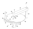
図2は、図1に示す第2洗浄ユニット18として使用される、本発明の実施形態に係る基板洗浄装置の概要を示す斜視図で、図3は、図2に示す第2洗浄ユニット18における基板と洗浄部材との関係を示す斜視図である。
FIG. 2 is a perspective view showing an outline of the substrate cleaning apparatus according to the embodiment of the present invention used as the
図2及び図3に示すように、本発明の実施形態の基板洗浄装置としての第2洗浄ユニット18は、半導体ウエハ等の基板Wを保持し回転させる基板保持機構40と、基板保持機構40で保持される基板Wの側方に配置された回転自在な支持軸42と、この支持軸42の上端に基部を連結した水平方向に延びる揺動アーム44を備えている。揺動アーム44の自由端(先端)には、例えばPVAスポンジから成り、略鉛直方向に延びる回転軸O1を中心に回転するペンシル型洗浄部材46が上下動自在かつ自転自在に取付けられている。このペンシル型洗浄部材46の直径は、基板Wの直径より小さく設定されている。更に、基板保持機構40で保持される基板Wの側方かつ上方に位置して、水平に回転している基板Wの表面に洗浄液を供給する洗浄液供給ノズル48が配置されている。
As shown in FIGS. 2 and 3, the
基板保持機構40は、基板Wを水平状態に保持するチャック60を先端に装着した複数本(図示では4本)のアーム62を備えており、このアーム62の基端は、回転軸64と一体に回転する基台66に連結されている。これによって、基板保持機構40のチャック60で保持された基板Wは、矢印E方向に回転するようになっている。
The
ペンシル型洗浄部材46は、支持軸42の回転に伴う揺動アーム44の揺動によって、図3に矢印Mで示すように、基板Wの略半径方向に沿って、基板Wのほぼ中心から基板の外周縁に向かって移動する。
The pencil-
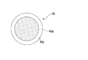
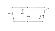
ペンシル型の洗浄部材46は、図4乃至図6に詳細に示すように、下端接触面46aの面積(直径D1)よりも上端面46bの面積(直径D2)の方が広くなっている(D1<D2)。ペンシル型洗浄部材46の中心を通る縦断面図を図6に示す。図6に示すように、ペンシル型洗浄部材46は、下端接触面46aと外周面46c上の直線(母線)とのなす角αが90°<α≦150°の逆円錐台形状を有している。この洗浄部材46の下端接触面46aと外周面46c上の直線とのなす角αは、90°<α≦120°であることが好ましく、95°<α≦120°であることが更に好ましい。
As shown in detail in FIGS. 4 to 6, the pencil-
第2洗浄ユニット18による基板Wの洗浄例を説明する。図2に示すように、先ず、基板保持機構40のチャック60で基板Wを水平に保持して回転させる。この基板Wの回転方向Eは、例えば図2及び図3に示すように、時計回り方向である。この水平に回転している基板Wの表面に洗浄液供給ノズル48から洗浄液を供給する。この時、ペンシル型の洗浄部材46は、基板Wの回転中心近傍の上方である洗浄開始位置A(図13参照)に位置している。
An example of cleaning the substrate W by the
次に、洗浄部材46を基板Wの回転方向Eとは逆の回転方向F(図2及び図3参照)に回転させながら下降させ、洗浄部材46の下端接触面46aを基板Wの表面に所定の押圧力で接触させる。そして、下端接触面46aを基板Wの表面に所定の押圧力で接触させながら、揺動アーム44を稼働させて、ペンシル型の洗浄部材46を、図3に示す、基板Wのほぼ半径方向に沿った移動方向Mに沿って、基板Wの外周縁の洗浄終了位置まで移動させる。これによって、基板Wの全表面の洗浄部材46によるスクラブ洗浄が行われる。
Next, the cleaning
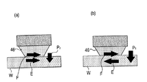
ここに、図7(a)に示すように、洗浄部材46の回転軸O1が鉛直軸O2と一致するようにして、回転軸O1を中心に洗浄部材46を回転させつつ、基板Wの外周縁に向け、移動方向Mに沿って洗浄部材46を移動させても良い。本実施例では、図7(b)に示すように、洗浄部材46の回転軸O1を洗浄部材46の移動方向Mと同じ方向に傾斜角θだけ傾斜させた状態で、つまり、洗浄部材46の回転軸O1を鉛直軸O2に対して傾斜角θだけM方向に傾斜させた状態で、回転軸O1を中心に洗浄部材46を回転させつつ、基板Wの外周縁に向け、移動方向Mに沿って洗浄部材46を移動させるようにしている。傾斜角θは、好ましくは1°〜15°である。傾斜角θを大きくしすぎると洗浄部材46と基板Wとの間に洗浄液が入りにくくなり、また洗浄部材46の傾斜により基板に圧力がかかりすぎ、接触面内での圧力分布が偏りすぎるという観点から傾斜角を1°以上15°以下(1°≦α≦15°)に設定している。ここで、傾斜角αは、1°以上でなくとも、洗浄部材46の回転軸O1が傾斜していない状態すなわち傾斜角が0°より大きければよい。
Here, as shown in FIG. 7 (a), the rotation axis O 1 of the cleaning
この時、前述のように、図6において、下端接触面46aと外周面46c上の直線とのなす角αが90°<α≦150°の逆円錐台形状を有している洗浄部材46を使用することで、下端接触面46aの一部が基板Wの表面から浮き上がってしまうことを防止することができる。
At this time, as described above, in FIG. 6, the cleaning
つまり、図8(a)に示すように、従来の一般的な円柱状の洗浄部材(以下、比較洗浄部材という)50を、その回転軸O3が鉛直軸O4と一致するようにして、回転軸O3を中心に回転させつつ、基板Wの外周縁に向け、移動方向Mに沿って比較洗浄部材50を移動させる場合には、比較洗浄部材50の下端接触面50aは基板Wの表面から浮き上がることはない。しかし、図8(b)に示すように、比較洗浄部材50の回転軸O3を比較洗浄部材50の移動方向Mと同じ方向に傾斜角θだけ傾斜させた状態で、回転軸O3を中心に比較洗浄部材50を回転させつつ、基板Wの外周縁に向け、移動方向Mに沿って移動させると、比較洗浄部材50の移動方向側の外周面に撓みによるくびれ部分52が発生し、この括れ部分52の下方にある下端接触面50aの部分が基板Wの表面から浮き上がってしまう。図8において、洗浄部材50の回転方向Fと基板Wの回転方向Eは同じ方向である。
That is, as shown in FIG. 8A, a conventional general columnar cleaning member (hereinafter referred to as a comparative cleaning member) 50 is arranged so that its rotation axis O 3 coincides with the vertical axis O 4 . When the
このように、比較洗浄部材50の下端接触面50aの一部が基板Wの表面から浮き上がる傾向にあると、比較洗浄部材50と基板Wとの間にパーティクル(ディフェクト)が保持され、この比較洗浄部材50と基板Wとの間に保持されたパーティクルが比較洗浄部材50の外部の基板W上に排出されて基板W上に残ってしまう。
Thus, when a part of the lower
本実施例では、洗浄部材46を逆円錐台形状にすることによって、洗浄部材46の回転軸O1を洗浄部材46の移動方向Mと同じ方向に傾斜角θだけ傾斜させた状態で、回転軸O1を中心に洗浄部材46を回転させつつ、基板Wの外周縁に向け、移動方向Mに沿って洗浄部材46を移動させても、下端接触面46aの一部が基板Wの表面から浮上ることがない。この場合、図9に示すように、洗浄部材46の変形量(撓み量)は、下端接触面46aが洗浄部材46の移動方向M側に向かうほど大きくなるため、洗浄部材46の基板Wの表面に対する接触圧力Pが洗浄部材46の移動方向Mに向かうほど大きくなるようにすることができる。
In this embodiment, the cleaning
つまり、洗浄部材46の基板Wの外周側により近い部分(図9において洗浄部材46の右半分部分)では洗浄部材46の基板Wの表面に対する接触圧力P1が相対的に大きく、洗浄部材46の基板Wの中心側により近い部分(図9において洗浄部材46の左半分部分)では洗浄部材46の基板Wの表面に対する接触圧力P2が相対的に小さくなる。これによって、洗浄部材46の基板Wの表面に対する接触圧力Pを調整して、基板Wの表面特性が疎水性であっても、基板Wの表面のほぼ全域を高い洗浄度で効率的に洗浄することができる。
In other words, the outer peripheral closer to the side portion of the substrate W in the cleaning
このように、洗浄部材46の基板Wの外周側により近い部分(図9において洗浄部材46の右半分部分)では、図10(b)に示すように、洗浄部材46の基板Wの表面に対する接触圧力P1が相対的に大きく、かつ基板Wと洗浄部材46の相対回転速度が比較的大きくなるようにすることで、この洗浄部材の部分での洗浄効率を高めることができる。一方、洗浄部材46の基板Wの中心側により近い部分(図9において洗浄部材46の左半分部分)では、図10(a)に示すように、洗浄部材46の基板Wの表面に対する接触圧力P2が相対的に小さく、かつ基板Wと洗浄部材46の相対回転速度が比較的小さくなるようにすることで、この洗浄部材の部分での基板Wの洗浄部材46からの逆汚染を少なくすることができる、これにより、高い洗浄性を維持して、基板の外周まで確実に洗浄することができる。
In this way, in the portion closer to the outer peripheral side of the substrate W of the cleaning member 46 (the right half portion of the cleaning
一方、図11に示すように、比較洗浄部材50の回転軸O3を鉛直軸O4と一致させ、回転軸O3を中心に比較洗浄部材50を回転させつつ、基板Wの外周縁に向け、移動方向Mに沿って比較洗浄部材50を移動させると、比較洗浄部材50の変形量(撓み量)が比較洗浄部材50の全域でほぼ一定となって、比較洗浄部材50の基板Wの表面に対する接触圧力P3が比較洗浄部材50の全域でほぼ一定となる。このため、比較洗浄部材50の基板Wの表面に対する接触圧力P3を比較洗浄部材50の移動方向Mに沿って次第に大きくなるように調整することができず、特に、特性が疎水性である基板表面のほぼ全域を高い洗浄度で効率的に洗浄することが困難となる。
On the other hand, as shown in FIG. 11, to match the rotation axis O 3 of
更に、基板Wの回転方向Eと比較洗浄部材50の回転方向Fを互いに同じ方向とすると、比較洗浄部材50の基板Wの中心側により近い部分(図11において比較洗浄部材50の左半分部分)では、基板Wの回転方向Eと比較洗浄部材50の回転方向Fが互いに逆方向となって、図12(a)に示すように、両者の相対回転速度が相対的に高く(両回転速度の和)なる。一方、比較洗浄部材50の基板Wの外周側により近い部分(図11において比較洗浄部材50の右半分部分)では、図12(b)に示すように、基板Wの回転方向Eと比較洗浄部材50の回転方向Fが互いに順方向となって、両者の相対回転速度が相対的に低く(両回転速度の差の絶対値)なる。
Further, if the rotation direction E of the substrate W and the rotation direction F of the
このため、比較洗浄部材50の基板Wの中心側に位置する部分では、高い洗浄性を確保できるものの、比較洗浄部材50の基板Wの外周側に位置する部分では、高い洗浄性を確保できず、比較洗浄部材50から基板Wへの逆汚染が生じて、基板Wの外周部での洗浄度が低下してしまう。
For this reason, although the high cleaning performance can be secured in the portion of the
なお、本実施例では、基板Wと洗浄部材46とを互いに逆方向に回転させているが、同じ方向に回転させてもよい。
In the present embodiment, the substrate W and the cleaning
図13に示すように、洗浄部材46の洗浄開始位置Aは、洗浄部材46が基板Wのほぼ半径方向に沿った移動方向Mに沿って移動する時、基板Wの回転中心O5付近を確実に通過するように、移動方向Mに沿って基板Wの回転中心O5より後方の位置に設定されている。つまり、洗浄部材46が洗浄開始位置Aに位置するとき、洗浄部材46の下端接触面46aは、基板Wの回転中心O5に触れることはなく、洗浄部材46が移動方向Mに沿って移動する時に、下端接触面46aが基板Wの回転中心O5上を通過するように構成されている。
As shown in FIG. 13, the cleaning start position A of the cleaning
洗浄部材46の洗浄開始位置Aを基板Wの外周縁近傍に設定し、洗浄部材46が基板Wの直径のほぼ全長に亘って移動し、その途中で、下端接触面46aが基板Wの回転中心
O5上を通過するようにしてもよい。
The cleaning start position A of the cleaning
また、洗浄部材46の回転軸O1を通り、洗浄部材46の移動方向Mに沿って延びる直線S1と、基板Wの回転中心O5を通り前記直線S1と平行な直線S2との距離Lは、0より大きく、洗浄部材46の下端接触部46aの半径R(=D1/2)よりも小さく(0<L<D1/2)設定されている。
In addition, as a rotation axis O 1 of the cleaning
これにより、洗浄部材46の下端接触面46aが基板Wの回転中心O5上を通り、かつ洗浄部材46の回転軸O1が基板Wの回転中心O5上を通らないようにして、基板Wの回転中心O5の無回転部分を洗浄部材46で確実に洗浄することができる。
Accordingly, the lower
洗浄液供給ノズル48として、基板W上に細長い矩形状に洗浄液が分布される洗浄ノズルではなく、基板W上に楕円状に洗浄液が分布される円錐ノズルが使用され、洗浄液供給ノズル48から供給された洗浄液が基板Wの回転中心O5付近まで直接または洗浄液の流れで達するように、洗浄液供給ノズル48が配置されている。更に、洗浄液供給ノズル48は、洗浄液供給ノズル48の噴射方向、つまり洗浄液供給ノズル48と基板Wの回転中心O5とを結ぶ直線S3と前記直線S2とがなす角度βが、60°〜120°となる位置に配置されている。このように洗浄液供給ノズル48を配置することにより、ペンシル型洗浄部材46が稼働する範囲に多量の新鮮な洗浄液を供給することができる。
ここでは、薬液供給ノズルとして円錐ノズルを使用し、楕円状に洗浄液が分布するようにしているが、ノズル形状や洗浄液の分布形状がこれらに限定されることはない。
The cleaning
Here, a conical nozzle is used as the chemical liquid supply nozzle so that the cleaning liquid is distributed in an elliptical shape, but the nozzle shape and the distribution shape of the cleaning liquid are not limited to these.
基板Wの表面に供給された洗浄液は、基板Wが水平に回転していることで遠心力を受けて、基板Wの表面への接触と同時に基板の外周方向に移動しながら、基板Wの全表面に拡がる。このため、前述のように、洗浄液供給ノズル48の洗浄部材46の移動方向Mに対する角度βを60°〜120°とすることで、新鮮で多量の洗浄液を洗浄部材46の下端接触面46aに供給することができる。
The cleaning liquid supplied to the surface of the substrate W receives centrifugal force due to the horizontal rotation of the substrate W, and moves in the outer peripheral direction of the substrate simultaneously with the contact with the surface of the substrate W. Spread on the surface. Therefore, as described above, the angle β with respect to the moving direction M of the cleaning
洗浄液供給ノズル48から供給された洗浄液が基板Wに接触する接触エリアCの基板Wに対する最外周位置と基板Wの回転中心O5との距離S4は、基板Wの半径の1/3以上であることが好ましく、このように洗浄液が基板Wに接触した状態で基板Wが回転すると、洗浄液は、基板Wの表面上に遠心力でより均一に拡がる。この接触エリアCの基板Wに対する最外周位置に位置する洗浄液は、基板Wの表面上において、遠心力によって基板Wの外周へ運搬される際、洗浄部材46の最外周位置Bよりも手前で基板Wの外周に排出されることが好ましい。このため、例えば、基板Wの表面が疎水性(接触角≧60°)の場合、基板の回転速度は、200rpm以上に設定される。
The distance S 4 between the outermost peripheral position of the contact area C where the cleaning liquid supplied from the cleaning
洗浄液の存在下で基板に洗浄部材を擦り付けて基板をスクラブ洗浄する場合、総合的な洗浄特性は、洗浄液を用いたパーティクル等の除去洗浄特性と洗浄部材の接触による接触洗浄特性の総和になる。この例のように、新鮮で多量の洗浄液を洗浄部材46の下端接触面46aに供給することで、高い洗浄特性を得るとともに、洗浄液の使用効率を高めることができる。
When scrub cleaning is performed by rubbing the cleaning member against the substrate in the presence of the cleaning liquid, the overall cleaning characteristics are the sum of the cleaning characteristics for removing particles and the like using the cleaning liquid and the contact cleaning characteristics due to the contact of the cleaning member. As in this example, by supplying a fresh and large amount of cleaning liquid to the lower
図1に示す基板処理装置では、ロードポート12内の基板カセットから取り出した基板の表面を、研磨ユニット14a〜14dのいずれかに搬送して研磨する。そして、研磨後の基板表面を第1洗浄ユニット(ロール洗浄ユニット)16で粗洗浄した後、第2洗浄ユニット(基板洗浄装置)18で仕上げ洗浄する。そして、洗浄後の基板を第2洗浄ユニット18から取り出し、乾燥ユニット20に搬入して乾燥させ、しかる後、乾燥後の基板をロードポート12の基板カセット内に戻す。
In the substrate processing apparatus shown in FIG. 1, the surface of the substrate taken out from the substrate cassette in the
接触洗浄の総合的な洗浄性は、洗浄部材の接触による汚染と洗浄特性の総和になる。そこで、洗浄部材の接触による基板への汚染を評価するため、表面特性が親水性のサンプル基板表面を、図2に示す第2洗浄ユニット(基板洗浄装置)18を使用して洗浄し、更に洗浄後のサンプル基板をスピン乾燥させた時に、サンプル基板表面に残った42nm以上のパーティクル(ディフェクト)の数を計測した時の結果を図14に実施例1として示す。同様にして、表面特性が疎水性のサンプル基板表面を、図2に示す第2洗浄ユニット(基板洗浄装置)18を使用して洗浄し、更に洗浄後のサンプル基板をIPA乾燥させた時に、サンプル基板表面に残った42nm以上のパーティクル(ディフェクト)の数を計測した時の結果を図14に実施例2として示す。 The overall cleanability of contact cleaning is the sum of contamination and cleaning characteristics due to contact of the cleaning member. Therefore, in order to evaluate the contamination of the substrate due to the contact of the cleaning member, the surface of the sample substrate having hydrophilic surface characteristics is cleaned using the second cleaning unit (substrate cleaning apparatus) 18 shown in FIG. FIG. 14 shows a result of Example 1 when the number of particles (defects) of 42 nm or more remaining on the surface of the sample substrate was measured when the subsequent sample substrate was spin-dried. Similarly, when the surface of the sample substrate having a hydrophobic surface characteristic is cleaned using the second cleaning unit (substrate cleaning apparatus) 18 shown in FIG. 2, and the sample substrate after the cleaning is IPA dried, The result when the number of particles (defects) of 42 nm or more remaining on the substrate surface is measured is shown as Example 2 in FIG.
図14には、従来の一般的な洗浄ユニットを使用して、表面特性が親水性のサンプル基板表面を洗浄し、その他は実施例1と同様にして、サンプル基板表面に残った42nm以上のパーティクル(ディフェクト)の数を計測した時の結果を比較例1として、同様にして、表面特性が疎水性のサンプル基板表面に残った42nm以上のパーティクル(ディフェクト)の数を計測した時の結果を比較例2として示している。 In FIG. 14, the surface of the sample substrate having a hydrophilic surface characteristic is cleaned using a conventional general cleaning unit, and the rest of the particles of 42 nm or more remaining on the sample substrate surface are the same as in Example 1. Similarly, the result when the number of (defects) was measured was set as Comparative Example 1, and the results when the number of particles (defects) of 42 nm or more remaining on the surface of the sample substrate having a hydrophobic surface property were similarly compared. This is shown as Example 2.
図14において、ディフェクト数は、比較例を100%として、実施例のディフェクト数を比較例に対する百分率で示している。図15においても同様に示す。 In FIG. 14, the number of defects is shown as a percentage of the comparative example with the number of defects in the example being 100% as a comparative example. This is also shown in FIG.
図14から、実施例1、2は、比較例1,2に比較して、洗浄後にサンプル基板表面に残存する42nm以上のディフェクト数を格段(親水性表面では70.69%、疎水性表面では0.22%)に減少させて汚染を防止することができることが判る。この効果は、基板表面が疎水性の性状の場合に顕著であることが判る。 From FIG. 14, in Examples 1 and 2, compared to Comparative Examples 1 and 2, the number of defects of 42 nm or more remaining on the surface of the sample substrate after cleaning was remarkably (70.69% on the hydrophilic surface, and on the hydrophobic surface). It can be seen that the contamination can be prevented by decreasing to 0.22%). It can be seen that this effect is significant when the substrate surface is hydrophobic.
表面特性が疎水性のlow-k膜(k=2.4)を表面に形成したサンプル基板の該表面(low-k膜)を研磨ユニットで研磨し、研磨後のサンプル基板表面を、前述と同様にして、図2に示す第2洗浄ユニット(基板洗浄装置)18を使用して洗浄し、更に洗浄後のサンプル基板をIPA乾燥させた時に、サンプル基板表面に残った100nm以上のパーティクル(ディフェクト)の数を計測した時の結果を図15に実施例3として示す。サンプル基板表面(low-k膜表面)を研磨し、従来の一般的な洗浄ユニットを使用して研磨後のサンプル基板表面を洗浄した。洗浄後のサンプル基板をIPA乾燥させ、実施例3と同様に100nm以上のパーティクル(ディフェクト)の数を計測した。計測した時の結果を比較例3として図15に示している。 The surface (low-k film) of a sample substrate on which a low-k film (k = 2.4) having a hydrophobic surface characteristic is formed is polished by a polishing unit, and the sample substrate surface after polishing is Similarly, when cleaning is performed using the second cleaning unit (substrate cleaning apparatus) 18 shown in FIG. 2 and the sample substrate after the cleaning is further subjected to IPA drying, particles of 100 nm or more remaining on the surface of the sample substrate (defects) ) Is shown as Example 3 in FIG. The sample substrate surface (low-k film surface) was polished, and the polished sample substrate surface was cleaned using a conventional general cleaning unit. The washed sample substrate was IPA dried, and the number of particles (defects) of 100 nm or more was measured in the same manner as in Example 3. The measurement results are shown as Comparative Example 3 in FIG.
図15から、実施例は、比較例に比較して、洗浄後にサンプル基板表面に残存する100nm以上のディフェクト数を格段(約30%減)に減少させ得ることが判る。 From FIG. 15, it can be seen that the example can remarkably reduce the number of defects of 100 nm or more remaining on the surface of the sample substrate after the cleaning as compared with the comparative example (about 30% reduction).
本発明によれば、たとえ基板の表面特性が疎水性であっても、基板の表面を高い洗浄度で洗浄することができる。つまり、配線金属として銅を使用し、絶縁膜としてlow−k膜を採用してダマシン配線を形成し、CMPによって、表面が疎水性の銅及びlow−k膜が露出した基板表面であっても、この基板表面を高い洗浄度で洗浄して表面に残存するディフェクト数を低減することができる。 According to the present invention, the surface of the substrate can be cleaned with a high degree of cleaning even if the surface characteristics of the substrate are hydrophobic. That is, even if copper is used as a wiring metal, a low-k film is used as an insulating film to form a damascene wiring, and the surface of the substrate is exposed by hydrophobic copper and a low-k film by CMP. The number of defects remaining on the surface can be reduced by cleaning the substrate surface with a high degree of cleaning.
これまで本発明の一実施形態について説明したが、本発明は上述の実施形態に限定されず、その技術的思想の範囲内において種々異なる形態にて実施されてよいことは言うまでもない。 Although one embodiment of the present invention has been described so far, it is needless to say that the present invention is not limited to the above-described embodiment, and may be implemented in various forms within the scope of the technical idea.
14a〜14d 研磨ユニット
16 第1洗浄ユニット
18 第2洗浄ユニット(基板洗浄装置)
20 乾燥ユニット
24 搬送ユニット
30 制御部
40 基板保持機構
44 揺動アーム
46 洗浄部材
46a 下端接触面
46b 上端面
46c 外周面
48 洗浄液供給ノズル
50 比較洗浄部材
14a to
20 Drying unit 24
Claims (7)
前記洗浄部材は、下端接触面と外周面上の直線とのなす角αが90°<α≦150°の逆円錐台形状を有し、
前記洗浄部材の回転軸を該洗浄部材の移動方向と同じ方向に傾斜させながら、前記洗浄部材の下端接触面の全面を基板に接触させつつ前記洗浄部材を一方向に向けて移動させることを特徴とする基板洗浄装置。 The cleaning member is moved in one direction while rotating around a rotating shaft extending in the vertical direction, and the lower end contact surface of the cleaning member is rubbed against the surface of the substrate rotating horizontally in the presence of the cleaning liquid. In the substrate cleaning apparatus for cleaning the surface,
The cleaning member has an inverted frustoconical shape in which an angle α formed between a lower end contact surface and a straight line on the outer peripheral surface is 90 ° <α ≦ 150 ° ,
The cleaning member is moved in one direction while inclining the rotating shaft of the cleaning member in the same direction as the moving direction of the cleaning member, while bringing the entire lower end contact surface of the cleaning member into contact with the substrate. Substrate cleaning device.
前記洗浄部材は、下端接触面と外周面上の直線とのなす角αが90°<α≦150°の逆円錐台形状を有し、The cleaning member has an inverted frustoconical shape in which an angle α formed between a lower end contact surface and a straight line on the outer peripheral surface is 90 ° <α ≦ 150 °,
前記洗浄部材を基板の表面に対して傾斜させながら、前記洗浄部材の下端接触面の全面を基板に接触させつつ前記洗浄部材を一方向に向けて移動させることを特徴とする基板洗浄装置。A substrate cleaning apparatus, wherein the cleaning member is moved in one direction while inclining the cleaning member with respect to the surface of the substrate and bringing the entire lower end contact surface of the cleaning member into contact with the substrate.
Priority Applications (4)
| Application Number | Priority Date | Filing Date | Title |
|---|---|---|---|
| JP2013238224A JP6297308B2 (en) | 2012-12-06 | 2013-11-18 | Substrate cleaning apparatus and substrate cleaning method |
| KR1020130148922A KR102103321B1 (en) | 2012-12-06 | 2013-12-03 | Substrate cleaning apparatus and substrate cleaning method |
| TW102144346A TWI611848B (en) | 2012-12-06 | 2013-12-04 | Substrate cleaning device and substrate cleaning method |
| US14/098,471 US9058977B2 (en) | 2012-12-06 | 2013-12-05 | Substrate cleaning apparatus and substrate cleaning method |
Applications Claiming Priority (3)
| Application Number | Priority Date | Filing Date | Title |
|---|---|---|---|
| JP2012267568 | 2012-12-06 | ||
| JP2012267568 | 2012-12-06 | ||
| JP2013238224A JP6297308B2 (en) | 2012-12-06 | 2013-11-18 | Substrate cleaning apparatus and substrate cleaning method |
Publications (3)
| Publication Number | Publication Date |
|---|---|
| JP2014132639A JP2014132639A (en) | 2014-07-17 |
| JP2014132639A5 JP2014132639A5 (en) | 2016-11-17 |
| JP6297308B2 true JP6297308B2 (en) | 2018-03-20 |
Family
ID=50879637
Family Applications (1)
| Application Number | Title | Priority Date | Filing Date |
|---|---|---|---|
| JP2013238224A Active JP6297308B2 (en) | 2012-12-06 | 2013-11-18 | Substrate cleaning apparatus and substrate cleaning method |
Country Status (4)
| Country | Link |
|---|---|
| US (1) | US9058977B2 (en) |
| JP (1) | JP6297308B2 (en) |
| KR (1) | KR102103321B1 (en) |
| TW (1) | TWI611848B (en) |
Families Citing this family (3)
| Publication number | Priority date | Publication date | Assignee | Title |
|---|---|---|---|---|
| CN107148665B (en) * | 2014-10-31 | 2018-04-20 | 株式会社荏原制作所 | Base plate cleaning device and substrate-cleaning method |
| JP6871499B2 (en) * | 2016-06-16 | 2021-05-12 | サミー株式会社 | Pachinko game machine |
| WO2023145431A1 (en) * | 2022-01-31 | 2023-08-03 | Agc株式会社 | Substrate cleaning method, glass substrate manufacturing method, euvl mask blank manufacturing method, and substrate cleaning apparatus |
Family Cites Families (18)
| Publication number | Priority date | Publication date | Assignee | Title |
|---|---|---|---|---|
| JP2628168B2 (en) | 1987-07-14 | 1997-07-09 | 住友シチックス株式会社 | Surface treatment equipment for semiconductor wafers |
| JP3447869B2 (en) * | 1995-09-20 | 2003-09-16 | 株式会社荏原製作所 | Cleaning method and apparatus |
| JP3302873B2 (en) | 1995-12-05 | 2002-07-15 | 東京エレクトロン株式会社 | Cleaning method and cleaning equipment |
| JPH09260322A (en) * | 1996-03-26 | 1997-10-03 | Nippon Steel Corp | Cleaner |
| JPH10199844A (en) * | 1997-01-10 | 1998-07-31 | Dainippon Screen Mfg Co Ltd | Substrate cleaning device |
| JPH10308374A (en) | 1997-03-06 | 1998-11-17 | Ebara Corp | Method and equipment for cleaning |
| JPH10312982A (en) | 1997-05-12 | 1998-11-24 | Dainippon Screen Mfg Co Ltd | Substrate-cleaning device |
| JPH10312983A (en) | 1997-05-12 | 1998-11-24 | Dainippon Screen Mfg Co Ltd | Substrate-cleaning device |
| JP4268239B2 (en) * | 1998-06-29 | 2009-05-27 | 芝浦メカトロニクス株式会社 | Brush cleaning apparatus and brush cleaning method |
| JP4091187B2 (en) | 1998-12-08 | 2008-05-28 | 株式会社荏原製作所 | Cleaning tool, substrate cleaning apparatus and substrate cleaning method |
| JP2002018368A (en) | 2000-07-05 | 2002-01-22 | Dainippon Screen Mfg Co Ltd | Substrate treating tool |
| US6648979B2 (en) * | 2001-01-24 | 2003-11-18 | International Business Machines Corporation | Apparatus and method for wafer cleaning |
| JP2003031536A (en) | 2001-07-12 | 2003-01-31 | Nec Corp | Cleaning method of wafer |
| JP2004273961A (en) * | 2003-03-12 | 2004-09-30 | Ebara Corp | Cleaning device of metal wiring forming substrate |
| JP2005012238A (en) * | 2004-09-02 | 2005-01-13 | Ebara Corp | Method and apparatus for cleaning substrate |
| JP2006073788A (en) * | 2004-09-02 | 2006-03-16 | Sumco Corp | Washing method and washing unit for wafer |
| JP2007273608A (en) * | 2006-03-30 | 2007-10-18 | Dainippon Screen Mfg Co Ltd | Substrate-treating apparatus and substrate treatment method |
| JP5336799B2 (en) | 2008-09-24 | 2013-11-06 | 東京エレクトロン株式会社 | Chemical mechanical polishing apparatus, chemical mechanical polishing method and control program |
-
2013
- 2013-11-18 JP JP2013238224A patent/JP6297308B2/en active Active
- 2013-12-03 KR KR1020130148922A patent/KR102103321B1/en active IP Right Grant
- 2013-12-04 TW TW102144346A patent/TWI611848B/en active
- 2013-12-05 US US14/098,471 patent/US9058977B2/en active Active
Also Published As
| Publication number | Publication date |
|---|---|
| KR20140073428A (en) | 2014-06-16 |
| US20140158160A1 (en) | 2014-06-12 |
| KR102103321B1 (en) | 2020-04-22 |
| TWI611848B (en) | 2018-01-21 |
| JP2014132639A (en) | 2014-07-17 |
| US9058977B2 (en) | 2015-06-16 |
| TW201429567A (en) | 2014-08-01 |
Similar Documents
| Publication | Publication Date | Title |
|---|---|---|
| JP5866227B2 (en) | Substrate cleaning method | |
| JP6265702B2 (en) | Substrate cleaning apparatus and substrate cleaning method | |
| US20190088510A1 (en) | Substrate cleaning device, substrate cleaning method, substrate processing device, and substrate drying device | |
| JP6312534B2 (en) | Substrate cleaning device | |
| US10737301B2 (en) | Substrate cleaning apparatus | |
| US9466512B2 (en) | Substrate cleaning apparatus and substrate processing apparatus | |
| CN107086190B (en) | Substrate cleaning apparatus and substrate processing apparatus | |
| JP6297308B2 (en) | Substrate cleaning apparatus and substrate cleaning method | |
| JP6029975B2 (en) | Substrate cleaning apparatus and substrate cleaning method | |
| JP2014130883A (en) | Substrate cleaning apparatus and substrate cleaning method | |
| TWI810835B (en) | Drying system with integrated substrate alignment stage | |
| JP6934918B2 (en) | Substrate cleaning equipment | |
| JP6431159B2 (en) | Substrate cleaning device | |
| JP6612176B2 (en) | Substrate cleaning device | |
| JP2023156015A (en) | Substrate cleaning device and substrate processing method |
Legal Events
| Date | Code | Title | Description |
|---|---|---|---|
| A521 | Request for written amendment filed |
Free format text: JAPANESE INTERMEDIATE CODE: A523 Effective date: 20160930 |
|
| A621 | Written request for application examination |
Free format text: JAPANESE INTERMEDIATE CODE: A621 Effective date: 20160930 |
|
| A131 | Notification of reasons for refusal |
Free format text: JAPANESE INTERMEDIATE CODE: A131 Effective date: 20170801 |
|
| A521 | Request for written amendment filed |
Free format text: JAPANESE INTERMEDIATE CODE: A523 Effective date: 20170927 |
|
| TRDD | Decision of grant or rejection written | ||
| A01 | Written decision to grant a patent or to grant a registration (utility model) |
Free format text: JAPANESE INTERMEDIATE CODE: A01 Effective date: 20180206 |
|
| A61 | First payment of annual fees (during grant procedure) |
Free format text: JAPANESE INTERMEDIATE CODE: A61 Effective date: 20180221 |
|
| R150 | Certificate of patent or registration of utility model |
Ref document number: 6297308 Country of ref document: JP Free format text: JAPANESE INTERMEDIATE CODE: R150 |
|
| R250 | Receipt of annual fees |
Free format text: JAPANESE INTERMEDIATE CODE: R250 |
|
| R250 | Receipt of annual fees |
Free format text: JAPANESE INTERMEDIATE CODE: R250 |
|
| R250 | Receipt of annual fees |
Free format text: JAPANESE INTERMEDIATE CODE: R250 |
|
| R250 | Receipt of annual fees |
Free format text: JAPANESE INTERMEDIATE CODE: R250 |