JP6231279B2 - Semiconductor device - Google Patents
Semiconductor device Download PDFInfo
- Publication number
- JP6231279B2 JP6231279B2 JP2013009217A JP2013009217A JP6231279B2 JP 6231279 B2 JP6231279 B2 JP 6231279B2 JP 2013009217 A JP2013009217 A JP 2013009217A JP 2013009217 A JP2013009217 A JP 2013009217A JP 6231279 B2 JP6231279 B2 JP 6231279B2
- Authority
- JP
- Japan
- Prior art keywords
- region
- probe
- bonding
- circuit element
- area
- Prior art date
- Legal status (The legal status is an assumption and is not a legal conclusion. Google has not performed a legal analysis and makes no representation as to the accuracy of the status listed.)
- Active
Links
- 239000004065 semiconductor Substances 0.000 title claims description 36
- 239000000523 sample Substances 0.000 claims description 73
- 239000000758 substrate Substances 0.000 claims description 20
- RYGMFSIKBFXOCR-UHFFFAOYSA-N Copper Chemical compound [Cu] RYGMFSIKBFXOCR-UHFFFAOYSA-N 0.000 claims description 10
- 229910052802 copper Inorganic materials 0.000 claims description 6
- 239000010949 copper Substances 0.000 claims description 6
- 238000000691 measurement method Methods 0.000 claims description 3
- 229910052751 metal Inorganic materials 0.000 description 14
- 239000002184 metal Substances 0.000 description 14
- 238000005259 measurement Methods 0.000 description 3
- XUIMIQQOPSSXEZ-UHFFFAOYSA-N Silicon Chemical compound [Si] XUIMIQQOPSSXEZ-UHFFFAOYSA-N 0.000 description 2
- 230000002411 adverse Effects 0.000 description 2
- 230000015572 biosynthetic process Effects 0.000 description 2
- PCHJSUWPFVWCPO-UHFFFAOYSA-N gold Chemical compound [Au] PCHJSUWPFVWCPO-UHFFFAOYSA-N 0.000 description 2
- 239000010931 gold Substances 0.000 description 2
- 229910052737 gold Inorganic materials 0.000 description 2
- 239000011229 interlayer Substances 0.000 description 2
- 238000004519 manufacturing process Methods 0.000 description 2
- 239000000463 material Substances 0.000 description 2
- 238000000034 method Methods 0.000 description 2
- 230000001681 protective effect Effects 0.000 description 2
- 229910052710 silicon Inorganic materials 0.000 description 2
- 239000010703 silicon Substances 0.000 description 2
- 229910052782 aluminium Inorganic materials 0.000 description 1
- XAGFODPZIPBFFR-UHFFFAOYSA-N aluminium Chemical compound [Al] XAGFODPZIPBFFR-UHFFFAOYSA-N 0.000 description 1
- 239000003990 capacitor Substances 0.000 description 1
- 230000000295 complement effect Effects 0.000 description 1
- 150000001875 compounds Chemical class 0.000 description 1
- 230000006870 function Effects 0.000 description 1
- 238000007689 inspection Methods 0.000 description 1
- 239000012212 insulator Substances 0.000 description 1
- 239000010410 layer Substances 0.000 description 1
- 229910044991 metal oxide Inorganic materials 0.000 description 1
- 150000004706 metal oxides Chemical class 0.000 description 1
- 230000009466 transformation Effects 0.000 description 1
Images


Classifications
-
- H—ELECTRICITY
- H01—ELECTRIC ELEMENTS
- H01L—SEMICONDUCTOR DEVICES NOT COVERED BY CLASS H10
- H01L2224/00—Indexing scheme for arrangements for connecting or disconnecting semiconductor or solid-state bodies and methods related thereto as covered by H01L24/00
- H01L2224/01—Means for bonding being attached to, or being formed on, the surface to be connected, e.g. chip-to-package, die-attach, "first-level" interconnects; Manufacturing methods related thereto
- H01L2224/02—Bonding areas; Manufacturing methods related thereto
- H01L2224/0212—Auxiliary members for bonding areas, e.g. spacers
- H01L2224/02122—Auxiliary members for bonding areas, e.g. spacers being formed on the semiconductor or solid-state body
- H01L2224/02163—Auxiliary members for bonding areas, e.g. spacers being formed on the semiconductor or solid-state body on the bonding area
- H01L2224/02165—Reinforcing structures
- H01L2224/02166—Collar structures
-
- H—ELECTRICITY
- H01—ELECTRIC ELEMENTS
- H01L—SEMICONDUCTOR DEVICES NOT COVERED BY CLASS H10
- H01L2224/00—Indexing scheme for arrangements for connecting or disconnecting semiconductor or solid-state bodies and methods related thereto as covered by H01L24/00
- H01L2224/01—Means for bonding being attached to, or being formed on, the surface to be connected, e.g. chip-to-package, die-attach, "first-level" interconnects; Manufacturing methods related thereto
- H01L2224/42—Wire connectors; Manufacturing methods related thereto
- H01L2224/44—Structure, shape, material or disposition of the wire connectors prior to the connecting process
- H01L2224/45—Structure, shape, material or disposition of the wire connectors prior to the connecting process of an individual wire connector
- H01L2224/45001—Core members of the connector
- H01L2224/45099—Material
- H01L2224/451—Material with a principal constituent of the material being a metal or a metalloid, e.g. boron (B), silicon (Si), germanium (Ge), arsenic (As), antimony (Sb), tellurium (Te) and polonium (Po), and alloys thereof
- H01L2224/45138—Material with a principal constituent of the material being a metal or a metalloid, e.g. boron (B), silicon (Si), germanium (Ge), arsenic (As), antimony (Sb), tellurium (Te) and polonium (Po), and alloys thereof the principal constituent melting at a temperature of greater than or equal to 950°C and less than 1550°C
- H01L2224/45147—Copper (Cu) as principal constituent
-
- H—ELECTRICITY
- H01—ELECTRIC ELEMENTS
- H01L—SEMICONDUCTOR DEVICES NOT COVERED BY CLASS H10
- H01L2924/00—Indexing scheme for arrangements or methods for connecting or disconnecting semiconductor or solid-state bodies as covered by H01L24/00
- H01L2924/0001—Technical content checked by a classifier
- H01L2924/0002—Not covered by any one of groups H01L24/00, H01L24/00 and H01L2224/00
-
- H—ELECTRICITY
- H01—ELECTRIC ELEMENTS
- H01L—SEMICONDUCTOR DEVICES NOT COVERED BY CLASS H10
- H01L2924/00—Indexing scheme for arrangements or methods for connecting or disconnecting semiconductor or solid-state bodies as covered by H01L24/00
- H01L2924/10—Details of semiconductor or other solid state devices to be connected
- H01L2924/11—Device type
- H01L2924/13—Discrete devices, e.g. 3 terminal devices
- H01L2924/1304—Transistor
- H01L2924/1306—Field-effect transistor [FET]
- H01L2924/13091—Metal-Oxide-Semiconductor Field-Effect Transistor [MOSFET]
Description
本発明は、ワイヤボンディング用パッド領域を備えた半導体装置に関する。 The present invention relates to a semiconductor device having a wire bonding pad region.
IC(Integrated Circuit)等の半導体装置は、外部から信号を入出力するための電極パッドを備えている。この電極パッドは、ワイヤボンディングによる配線接続のための用途に加えて、半導体装置の動作確認等の検査を行う際にテストプローブを接触させるための用途に使用されることがある。 A semiconductor device such as an IC (Integrated Circuit) includes electrode pads for inputting and outputting signals from the outside. In addition to the use for wiring connection by wire bonding, the electrode pad may be used for a purpose of bringing a test probe into contact when performing an inspection such as operation check of the semiconductor device.
しかし、上記のように、電極パッドをテストプローブの接触用パッドとワイヤボンディング用パッドとに兼用すると、プローブによる針跡が形成されるためにボンディングの信頼性が低下するという問題があった。そこで、このような形態で使用する電極パッドでは、テストプローブの接触用パッドと、ワイヤボンディング用パッドのそれぞれに分けて形成することが行われていた。 However, as described above, when the electrode pad is used as both the contact pad for the test probe and the wire bonding pad, there is a problem in that the needle trace is formed by the probe and bonding reliability is lowered. Therefore, the electrode pads used in such a form have been formed separately for the contact pads of the test probe and the wire bonding pads.
ところで、ボンディングワイヤとしては、コストの高い金系の材料に代えて、銅系の材料を適用したいという要求がある。しかし、銅は金に比較して硬度が高いため、銅ワイヤを用いてワイヤボンディングを行う際には電極パッドに強い荷重をかけて行う必要がある。このため、銅ワイヤをボンディングする際に、ボンディング用パッド下部の回路素子にダメージが与えられる可能性が大きくなるという問題がある。従って、ボンディング用パッドを回路形成領域に配置することができず、またプローブ用パッドと兼用することもできないため、チップ面積が増大するという問題があった。 By the way, as a bonding wire, there is a demand for applying a copper-based material instead of a costly gold-based material. However, since copper has a higher hardness than gold, it is necessary to apply a heavy load to the electrode pad when wire bonding is performed using a copper wire. For this reason, when bonding a copper wire, there exists a problem that possibility that a circuit element under the pad for bonding will be damaged becomes large. Therefore, the bonding pad cannot be arranged in the circuit formation region, and cannot be used as the probe pad, and there is a problem that the chip area increases.
本発明は上記事情に鑑みてなされたものであり、その目的は、ICチップの面積増大を回避し、回路素子にダメージが与えられることがない銅ワイヤボンディングに適用可能な半導体装置を提供することにある。 The present invention has been made in view of the above circumstances, and an object thereof is to provide a semiconductor device applicable to copper wire bonding which avoids an increase in the area of an IC chip and does not damage circuit elements. It is in.
請求項1に記載の発明による半導体装置は、半導体基板と、前記半導体基板上に形成された回路素子とを有する。また、それぞれが独立して設けられ、相互に電気的に接続されたプローブ用パッド領域と複数のボンディング用パッド領域とを有している。複数のボンディング用パッド領域は銅ワイヤによるボンディングの接続が可能な領域である。プローブ用パッド領域の下部には、半導体装置の組立後の電子回路動作に寄与する回路素子が形成されており、複数のボンディング用パッド領域の下部には、半導体装置の組立後の電子回路動作に寄与する回路素子が形成されていない。プローブ用パッド領域と複数のボンディング用パッド領域は、半導体基板上方に設けられた同一でひと続きの配線上に設けられており、配線上に設けられた絶縁膜に形成された開口窓によって区画されており、同一の配線上に銅ワイヤによるボンディングの接続がされる。 According to a first aspect of the present invention, a semiconductor device includes a semiconductor substrate and a circuit element formed on the semiconductor substrate. Each has a probe pad region and a plurality of bonding pad regions which are provided independently and electrically connected to each other. The plurality of bonding pad regions are regions that can be bonded by copper wires. A circuit element that contributes to the electronic circuit operation after the assembly of the semiconductor device is formed below the probe pad region, and an electronic circuit operation after the assembly of the semiconductor device is formed below the plurality of bonding pad regions. Contributing circuit elements are not formed. The probe pad area and the plurality of bonding pad areas are provided on the same continuous wiring provided above the semiconductor substrate, and are defined by an opening window formed in an insulating film provided on the wiring. Bonding with a copper wire is made on the same wiring.
この構成によれば、プローブ用パッド領域とボンディング用パッド領域が別々に設けられることにより、ボンディング用パッド領域にプローブの針跡が形成されることを回避できる。これにより、銅ボンディングワイヤとボンディング用パッド領域との密着性を向上させることができる。また、プローブ用パッド領域については、プローブ時の針当ての接触圧や接触回数を調整することによりプローブ用パッド領域の下に形成された回路素子へのダメージを回避できる。さらに、ボンディング用パッド領域の下にはIC製品の電子回路に使用される回路素子が形成されないため、銅ワイヤによるボンディング時にボンディング用パッド領域下部にダメージが与えられたとしても、IC製品としての動作に変動をきたすことがなく、IC製品の歩留に与える影響を小さくできる。 According to this configuration, the probe pad region and the bonding pad region are provided separately, so that it is possible to prevent the probe traces from being formed in the bonding pad region. As a result, the adhesion between the copper bonding wire and the bonding pad region can be improved. Further, with respect to the probe pad area, it is possible to avoid damage to the circuit elements formed under the probe pad area by adjusting the contact pressure and the number of times of contact with the probe during probe. Furthermore, since the circuit elements used for the electronic circuit of the IC product are not formed under the bonding pad area, even if damage is given to the lower part of the bonding pad area when bonding with the copper wire, the operation as an IC product is performed. The influence on the yield of IC products can be reduced.
(第1の実施形態)
以下、本発明の実施形態について図1から図4を参照しながら説明する。なお、以下の説明において、例えば回路素子配置禁止領域4と記述する場合は、回路素子配置禁止領域4a、4b、4cを含み、回路素子配置禁止領域4a、4b、4cと記述する場合は、個々の回路素子配置禁止領域を示すものとする。金属配線5、プローブ用パッド領域6、ボンディング用パッド領域7においても同様である。
(First embodiment)
Hereinafter, an embodiment of the present invention will be described with reference to FIGS. In the following description, for example, when describing as the circuit element arrangement prohibited
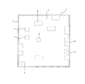
図1において、ICチップ(半導体装置)1を構成する半導体基板2上に、回路素子配置領域3、回路素子配置禁止領域4がレイアウトされている。回路素子配置領域3はICチップ1の回路を構成する複数の回路素子13(図3(b)参照)が形成される領域である。回路素子13には、各種トランジスタ、抵抗素子、容量素子などが含まれる。また、各種トランジスタには、CMOS(Complementary Metal Oxide Semiconductor)回路や、DMOS(Double-Diffused MOSFET)、LDMOS(Laterally Diffused MOSFET)等のパワー素子も含まれる。プローブ用パッド領域6は回路素子配置領域3上に設けられている。
In FIG. 1, a circuit
回路素子配置禁止領域4はICチップ1の回路を構成する回路素子が配置されていない領域である。ボンディング用パッド領域7は回路素子配置禁止領域4上に設けられている。同電位が与えられる一組のプローブ用パッド領域6及びボンディング用パッド領域7は、同一の金属配線5上に形成されている。例えば、4つのプローブ用パッド領域6a1、6a2、6a3、6a4及び一つのボンディング用パッド領域7aを有する電極パッド領域群Aの電極パッド領域は何れも同一の金属配線5a上に形成されている。従って、プローブ用パッド領域6a1、6a2、6a3、6a4とボンディング用パッド領域7aは電気的に接続されている。
The circuit element
図2を参照すると、半導体基板2上に、回路素子配置領域3及び回路素子配置禁止領域4がレイアウトされている。回路素子配置領域3は、ICチップ1端から所定幅を除いて全面に広がって形成されている。回路素子配置禁止領域4は、回路素子配置領域3のパターンに対して、ボンディング用パッド領域7の形状に対応して矩形の切り欠き形状若しくは矩形の穴を設けるような形状にレイアウトされている。
Referring to FIG. 2, a circuit
図1は、図2に示した回路素子配置領域3及び回路素子配置禁止領域4のレイアウトパターンに、プローブ用パッド領域6、ボンディング用パッド領域7及び金属配線5等のレイアウトパターンを重ね合わせたものである。
FIG. 1 shows the layout pattern of the
図3(a)はプローブ用パッド領域6とボンディング用パッド領域7とをそれぞれ1個ずつ模式的に並べて配置した基本構成に相当する平面図である。図3(b)は、図3(a)のAA線における断面図である。図3(b)においては、ボンディングワイヤ10及びプローブ針11を配置したときの状態をイメージ的に示している。
FIG. 3A is a plan view corresponding to a basic configuration in which the
図3(a)において、半導体基板2上に回路素子配置領域3及び回路素子配置禁止領域4が配置されている。回路素子配置禁止領域4は、回路素子配置領域3に対して矩形状の穴を設けるようにレイアウトされている。プローブ用パッド領域6は回路素子配置領域3上に配置されている。ボンディング用パッド領域7は回路素子配置禁止領域4上に配置されている。
In FIG. 3A, the circuit
図3(b)において、半導体基板2は、回路素子配置領域3と回路素子配置禁止領域4に区画されている。半導体基板2上であって回路素子配置領域3には、回路素子13が形成されている。回路素子13は層間絶縁膜12によって覆われており、層間絶縁膜12上には保護膜14が設けられている。保護膜14上には例えばアルミニウムによって形成された金属配線5が形成されている。ここで、回路素子13とは、ICチップ1の回路を構成するもので、組立後の電子回路動作に寄与する回路素子に相当する。回路素子13がダメージを受けるとICチップ1の動作に影響を及ぼすことになる。
In FIG. 3B, the
一方、回路素子配置禁止領域4は、回路素子13を形成しない領域として設定されているが、ICチップ1の動作に寄与ないテスト素子16であれば配置可能である。テスト素子16とは、例えばICチップ1の製造の途中工程における加工の出来栄えチェックのために設置される素子である。例としてMOSFETのゲート電極の線幅測定用パターン等が挙げられる。このようなテスト素子16であれば、ボンディング時にダメージを受けても、ICチップ1の電気的な回路動作に影響を及ぼさない。
On the other hand, the circuit element
金属配線5上であって、回路素子配置領域3の上方にはプローブ用パッド領域6が設けられている。回路素子配置禁止領域4の上方にはボンディング用パッド領域7が設けられている。プローブ用パッド領域6及びボンディング用パッド領域7は、金属配線5上を覆うように形成された絶縁膜15に開口窓17を設け、金属配線5の表面の一部を露出せしめるように区画された領域によって構成されている。プローブ用パッド領域6にはプローブ針11を接触させて電気的に導通させる。また、ボンディング用パッド領域7にボンディングワイヤ10が接続される。ボンディングワイヤ10は銅により形成されている。
A
また、プロービング時には、プロービングにおける針当ての接触圧や接触回数を最適となるように調整する。また、さらに金属配線5の膜厚は、プロービング時の荷重で下層に悪影響を与えないように、通常よりも厚くしている。これによりプローブ用パッド領域6の下に形成された回路素子13への悪影響を及ぼすことがないようにできる。
In probing, the contact pressure and the number of times of contact with the needle pad during probing are adjusted so as to be optimized. Furthermore, the film thickness of the
次に、図1において示した様々な電極パッド領域の配置について説明する。電極パッド領域群Aは、上述のように、複数のプローブ用パッド領域6a1、6a2、6a3、6a4と、一つのボンディング用パッド領域7aを有している。これら複数のプローブ用パッド領域6a1、6a2、6a3、6a4と、一つのボンディング用パッド領域7aは同一の金属配線5a上に設けられた絶縁膜15にそれぞれの電極パッド領域に対応して開口窓17を形成することによって金属配線5aの表面を露出せしめて区画した領域である。これらはICチップ1端から中ほどに向かって、ボンディング用パッド領域7a、プローブ用パッド領域6a1、6a2、6a3、6a4の順に隣接して並んでいる。
Next, the arrangement of various electrode pad regions shown in FIG. 1 will be described. As described above, the electrode pad region group A has a plurality of probe pad regions 6a1, 6a2, 6a3, 6a4 and one
プローブ用パッド領域6a1、6a2、6a3、6a4は回路素子配置領域3上に配置されている。ボンディング用パッド領域7aは回路素子配置禁止領域4上に配置されている。複数のプローブ用パッド領域6a1、6a2、6a3、6a4は例えば四端子測定法におけるセンス電極、フォース電極として使用することができる。あるいは、予備のプローブ用パッド領域6として使用することができる。プローブ用パッド領域6にプロービングを行うと、プローブ用パッド領域6表面にプローブ針11の針跡が形成される。ここに再度プロービングを行うと、プローブ針11とプローブ用パッド領域6表面との間の接触抵抗が変化する可能性がある。また、プローブ針11がプローブ用パッド領域6に繰り返して接触することで、回路素子13にも繰り返し荷重がかかる。複数のプローブ用パッド領域6を設けると、再度プロービングする場合に、一度プロービングしたプローブ用パッド領域6を使用せず、未だプロービングされておらず針跡が形成されていない予備のプローブ用パッド領域6を使用することができる。これにより、プローブ用パッド領域6の下部に位置する回路素子13への繰り返し荷重を防止しつつ、電気的測定の精度を向上させることができる。
The probe pad areas 6a1, 6a2, 6a3, 6a4 are arranged on the circuit
電極パッド領域群Bは、複数のプローブ用パッド領域6b1、6b2と、複数のボンディング用パッド領域7b1、7b2を有している。ICチップ1端に沿ってボンディング用パッド領域7b1、7b2が配置され、これに隣接してプローブ用パッド領域6b1、6b2が配置されている。プローブ用パッド領域6b1、6b2は回路素子配置領域3上に配置されている。ボンディング用パッド領域7b1、7b2は回路素子配置禁止領域4上に配置されている。プローブ用パッド領域6b1、6b2及びボンディング用パッド領域7b1、7b2は同一の金属配線5b上に設けられている。
The electrode pad region group B has a plurality of probe pad regions 6b1 and 6b2 and a plurality of bonding pad regions 7b1 and 7b2. Bonding pad regions 7b1 and 7b2 are disposed along the end of the
複数のプローブ用パッド領域6b1、6b2を有する理由は上述の場合と同じである。複数のボンディング用パッド領域7b1、7b2は、ボンディング用パッド領域7b1、7b2が接続される素子に対して、複数のボンディングワイヤを形成したい場合に利用することができる。例えば、当該ボンディング用パッド領域7b1、7b2に接続される回路素子13が、大電流を必要とするパワー素子である場合は、必要な電流を供給するために1本のワイヤボンディングでは不足である場合がある。このような場合に複数本のワイヤボンディングを形成できる。あるいは、ボンディング用パッド領域7b1、7b2を、例えばそれぞれ異なる外部端子に接続し、外部端子毎に制御を行い、ICチップ1に異なるファンクションをさせたい場合などに利用することができる。
The reason for having a plurality of probe pad regions 6b1 and 6b2 is the same as that described above. The plurality of bonding pad regions 7b1 and 7b2 can be used when a plurality of bonding wires are to be formed for the element to which the bonding pad regions 7b1 and 7b2 are connected. For example, when the
次に、電極パッド領域群Cは、回路素子配置禁止領域4が、回路素子配置領域3に囲まれるように配置されたレイアウトの場合を示している。電極パッド領域群Cの回路素子配置領域3c上には、プローブ用パッド領域6cが設けられている。回路素子配置禁止領域4c上にはボンディング用パッド領域7c1、7c2が設けられている。プローブ用パッド領域6c及びボンディング用パッド領域7c1、7c2は同一の金属配線5b上に設けられている。複数のボンディング用パッド領域7c1、7c2を有するのは上述の場合と同じである。プローブ用パッド領域6cが一つであるのは、例えば四端子測定法におけるセンス電極、フォース電極を必要としない場合である。
Next, the electrode pad region group C shows a layout in which the circuit element
上記のように、プローブ用パッド領域6と、ボンディング用パッド領域7を複数設けるレイアウトの例として、電極パッド領域群A、B、Cについて説明したが、これらは一例であって、電極パッド領域を設ける数や配置する位置は、目的や状況に応じて適宜選択することができる。
As described above, the electrode pad region groups A, B, and C have been described as an example of a layout in which a plurality of
この構成によれば、プローブ用パッド領域6を回路素子配置領域3上に配置するため、この領域分だけICチップ1の面積増大を回避することができる。また、ボンディング用パッド領域7は回路素子配置禁止領域4上に配置され、この下部にテスト素子16を配置することが可能なため、この領域分だけICチップ1の面積増大を回避することができる。従って、ウェハあたりの有効チップ数を増加させることができる。
According to this configuration, since the
また、プローブ用パッド領域6とボンディング用パッド領域7が別々に設けられることにより、ボンディング用パッド領域7にプローブ針11の針跡が形成されることを回避できる。これによりボンディングワイヤ10とボンディング用パッド領域7との密着性を向上させることができる。また、プローブ用パッド領域6については、プロービングにおける針当ての接触圧や接触回数を調整することによりプローブ用パッド領域6の下に形成された回路素子13へのダメージを回避できる。さらに、ボンディング用パッド領域7の下にはICチップ1の電子回路に使用される回路素子13が形成されないため、ボンディングワイヤ10のボンディング時にボンディング用パッド領域7の下部にダメージが与えられたとしても、IC製品としての動作に変動をきたすことがなく、IC製品の歩留に与える影響を小さくできる。
Further, by providing the
また、一つの電極パッド領域群A、B、Cについてプローブ用パッド領域6が複数設けられているため、複数回測定を行う場合に、一度ブロービングされてプローブ針11の針跡が形成されたプローブ用パッド領域6を再度使用することなくプロービングすることが可能となる。これにより、プローブ用パッド領域6の下部に位置する回路素子13への繰り返し荷重を防止しつつ、電気的測定の精度を向上させることができる。
Further, since a plurality of
また、一つの電極パッド領域群A、B、Cについてボンディング用パッド領域7が複数個設けられているため、複数のボンディングワイヤ10が必要な場合や、それぞれ異なる外部端子に接続したい場合に利用することができる。
Further, since a plurality of
(第2の実施形態)
次に図4を参照して、第2の実施形態について説明する。第1の実施形態と異なる点は、ウェハ状態のICチップ1間のスクライブ領域18の近傍に設けられたボンディング用パッド領域7の構成である。図4に示すように、スクライブ領域18は、ウェハ状態の半導体基板2上で隣接するICチップ1の回路素子配置領域3間にレイアウトされる。テスト素子領域19はスクライブ領域18を含むようにレイアウトされる。テスト素子領域19にはテスト素子16が配置される。ボンディング用パッド領域7は、その一部、若しくは、可能であれば全部がテスト素子領域19上に配置される。図4では、一例としてボンディング用パッド領域7の一部がテスト素子領域19上に配置されている状況を示している。スクライブ領域18とボンディング用パッド領域7との間の距離は、ダイシング時のダイシングブレード(図示せず)の位置合わせ精度を考慮して設定している。
(Second Embodiment)
Next, a second embodiment will be described with reference to FIG. The difference from the first embodiment is the configuration of the
この構成により、ボンディング用パッド領域7をスクライブ領域18周辺に設けられたテスト素子領域19上に配置することができるため、ボンディング用パッド領域7のうちテスト素子領域19上に配置された面積分だけ回路素子配置領域3の面積を増加させることができる。これによりチップ面積を縮小することができ、またウェハあたりの有効チップ数を増加させることができる。
With this configuration, the
(その他の実施形態)
以上、本発明の好適な実施形態について説明したが、本発明は上述した実施形態に限定されるものではなく、発明の要旨を逸脱しない範囲内で種々の変形、拡張を行うことができる。
(Other embodiments)
As mentioned above, although preferred embodiment of this invention was described, this invention is not limited to embodiment mentioned above, A various deformation | transformation and expansion | extension can be performed within the range which does not deviate from the summary of invention.
半導体基板は、シリコン基板、化合物半導体基板、SiC基板、あるいは、SOI(Silicon on Insulator)基板等、様々な半導体基板を用いることができる。
半導体装置としては、マイコン、メモリ、車載用LSI、その他の半導体装置に適用することができる。
As the semiconductor substrate, various semiconductor substrates such as a silicon substrate, a compound semiconductor substrate, an SiC substrate, or an SOI (Silicon on Insulator) substrate can be used.
As a semiconductor device, it can be applied to a microcomputer, a memory, an in-vehicle LSI, and other semiconductor devices.
テスト素子として、ICチップの製造の途中工程における加工の出来栄えチェックのために設置される素子を例示して説明したが、これに限定される必要はなく、例えば、単体のMOSトランジスタ、リングオシレータ等、ダイシングを行う前の半導体ウェハ状態での電気的な特性チェックのために設けられたテスト素子であっても良い。 As the test element, the element installed for checking the quality of processing in the process of manufacturing the IC chip has been described as an example. However, the present invention is not limited to this. For example, a single MOS transistor, ring oscillator, etc. Alternatively, it may be a test element provided for checking electrical characteristics in a semiconductor wafer state before dicing.
図面中、2は半導体基板、5、5a、5b、5cは金属配線、6、6a1、6a2、6a3、6a4、6b1、6b2、6cはプローブ用パッド領域、7、7a、7b1、7b2、7c1、7c2はボンディング用パッド領域、13は回路素子、15は絶縁膜、17は開口窓である。
In the drawing, 2 is a semiconductor substrate, 5, 5 a, 5 b, 5 c are metal wiring, 6, 6 a 1, 6 a 2, 6 a 3, 6 a 4, 6
Claims (3)
それぞれが独立して設けられ、相互に電気的に接続されたプローブ用パッド領域(6)と複数のボンディング用パッド領域(7)とを有し、
前記複数のボンディング用パッド領域は銅ワイヤによるボンディングの接続が可能な領域であり、
前記プローブ用パッド領域の下部には、前記半導体装置の組立後の電子回路動作に寄与する回路素子(13)が形成されており、前記複数のボンディング用パッド領域の下部には、前記半導体装置の組立後の電子回路動作に寄与する回路素子が形成されておらず、
前記プローブ用パッド領域と前記複数のボンディング用パッド領域は、前記半導体基板上方に設けられた同一でひと続きの配線(5)上に設けられており、前記配線上に設けられた絶縁膜(15)に形成された開口窓(17)によって区画されており、
前記同一の配線(5)上に銅ワイヤによるボンディングの接続がされることを特徴とする半導体装置。 A semiconductor device having a semiconductor substrate (2) and a circuit element formed on the semiconductor substrate,
Each has a probe pad region (6) and a plurality of bonding pad regions (7) that are independently provided and electrically connected to each other,
The plurality of bonding pad regions are regions where bonding of copper wires can be connected,
A circuit element (13) that contributes to an electronic circuit operation after the assembly of the semiconductor device is formed below the probe pad region, and below the plurality of bonding pad regions, Circuit elements that contribute to electronic circuit operation after assembly are not formed,
Wherein the plurality of bonding pad region and the probe pad region, the semiconductor is provided on a stretch of line (5) a substrate of the same which is provided above an insulating film (15 provided on the wiring ) Is defined by an opening window (17) formed in
A semiconductor device, wherein a bonding connection using a copper wire is made on the same wiring (5).
3. The semiconductor device according to claim 1, wherein the plurality of probe pad regions provided are sense terminals or force terminals in a four-terminal measurement method.
Priority Applications (1)
| Application Number | Priority Date | Filing Date | Title |
|---|---|---|---|
| JP2013009217A JP6231279B2 (en) | 2013-01-22 | 2013-01-22 | Semiconductor device |
Applications Claiming Priority (1)
| Application Number | Priority Date | Filing Date | Title |
|---|---|---|---|
| JP2013009217A JP6231279B2 (en) | 2013-01-22 | 2013-01-22 | Semiconductor device |
Publications (2)
| Publication Number | Publication Date |
|---|---|
| JP2014143236A JP2014143236A (en) | 2014-08-07 |
| JP6231279B2 true JP6231279B2 (en) | 2017-11-15 |
Family
ID=51424332
Family Applications (1)
| Application Number | Title | Priority Date | Filing Date |
|---|---|---|---|
| JP2013009217A Active JP6231279B2 (en) | 2013-01-22 | 2013-01-22 | Semiconductor device |
Country Status (1)
| Country | Link |
|---|---|
| JP (1) | JP6231279B2 (en) |
Families Citing this family (4)
| Publication number | Priority date | Publication date | Assignee | Title |
|---|---|---|---|---|
| JP6538960B2 (en) * | 2016-02-23 | 2019-07-03 | ルネサスエレクトロニクス株式会社 | Semiconductor device and method of manufacturing the same |
| JP6767789B2 (en) * | 2016-06-29 | 2020-10-14 | ローム株式会社 | Semiconductor device |
| JP2021150307A (en) * | 2020-03-16 | 2021-09-27 | ソニーセミコンダクタソリューションズ株式会社 | Semiconductor device, manufacturing method of the semiconductor device, and electronic apparatus |
| WO2024004876A1 (en) * | 2022-06-30 | 2024-01-04 | ソニーセミコンダクタソリューションズ株式会社 | Semiconductor device and layered structure |
Family Cites Families (3)
| Publication number | Priority date | Publication date | Assignee | Title |
|---|---|---|---|---|
| JP2536419B2 (en) * | 1993-07-23 | 1996-09-18 | 日本電気株式会社 | Semiconductor integrated circuit device |
| JP2005064218A (en) * | 2003-08-12 | 2005-03-10 | Renesas Technology Corp | Semiconductor device |
| JP4717523B2 (en) * | 2005-06-13 | 2011-07-06 | ルネサスエレクトロニクス株式会社 | Semiconductor device and manufacturing method thereof |
-
2013
- 2013-01-22 JP JP2013009217A patent/JP6231279B2/en active Active
Also Published As
| Publication number | Publication date |
|---|---|
| JP2014143236A (en) | 2014-08-07 |
Similar Documents
| Publication | Publication Date | Title |
|---|---|---|
| JP4512125B2 (en) | Semiconductor package group for detecting stress distribution and method for detecting stress distribution of semiconductor package using the same | |
| TWI730028B (en) | Semiconductor device and manufacturing method thereof | |
| US7777223B2 (en) | Semiconductor device | |
| JP2008258258A (en) | Semiconductor device | |
| US7834351B2 (en) | Semiconductor device | |
| WO2009084100A1 (en) | Semiconductor device and its manufacturing method | |
| JP6231279B2 (en) | Semiconductor device | |
| US20180286766A1 (en) | Manufacturing method of semiconductor device, semiconductor device, and inspection apparatus for semiconductor device | |
| JP5529611B2 (en) | Semiconductor device and resistance measuring method | |
| US20160178666A1 (en) | Alignment checking apparatus and integrated circuit including the same | |
| US11521904B2 (en) | Wire bond damage detector including a detection bond pad over a first and a second connected structures | |
| US8717059B2 (en) | Die having wire bond alignment sensing structures | |
| US20200303268A1 (en) | Semiconductor device including residual test pattern | |
| US20060071284A1 (en) | Easily crack checkable semiconductor device | |
| KR102195561B1 (en) | Electrical connection device | |
| JP2005303279A (en) | Semiconductor device | |
| JP2008028274A (en) | Manufacturing method for semiconductor device | |
| JP2012174789A (en) | Semiconductor device | |
| JP4877465B2 (en) | Semiconductor device, semiconductor device inspection method, semiconductor wafer | |
| JP3763664B2 (en) | Test circuit | |
| US20090014717A1 (en) | Test ic structure | |
| JPS62183134A (en) | Semiconductor device | |
| KR20010110157A (en) | Monitoring resistor element and measuring method of relative preciseness of resistor elements | |
| JPS62193137A (en) | Manufacture of semiconductor device | |
| US20080122446A1 (en) | Test pattern |
Legal Events
| Date | Code | Title | Description |
|---|---|---|---|
| A621 | Written request for application examination |
Free format text: JAPANESE INTERMEDIATE CODE: A621 Effective date: 20150515 |
|
| A131 | Notification of reasons for refusal |
Free format text: JAPANESE INTERMEDIATE CODE: A131 Effective date: 20151222 |
|
| A977 | Report on retrieval |
Free format text: JAPANESE INTERMEDIATE CODE: A971007 Effective date: 20151225 |
|
| A521 | Request for written amendment filed |
Free format text: JAPANESE INTERMEDIATE CODE: A523 Effective date: 20160219 |
|
| A02 | Decision of refusal |
Free format text: JAPANESE INTERMEDIATE CODE: A02 Effective date: 20160817 |
|
| A521 | Request for written amendment filed |
Free format text: JAPANESE INTERMEDIATE CODE: A523 Effective date: 20161007 |
|
| A911 | Transfer to examiner for re-examination before appeal (zenchi) |
Free format text: JAPANESE INTERMEDIATE CODE: A911 Effective date: 20161019 |
|
| A912 | Re-examination (zenchi) completed and case transferred to appeal board |
Free format text: JAPANESE INTERMEDIATE CODE: A912 Effective date: 20161216 |
|
| A521 | Request for written amendment filed |
Free format text: JAPANESE INTERMEDIATE CODE: A523 Effective date: 20170809 |
|
| A61 | First payment of annual fees (during grant procedure) |
Free format text: JAPANESE INTERMEDIATE CODE: A61 Effective date: 20171019 |
|
| R150 | Certificate of patent or registration of utility model |
Ref document number: 6231279 Country of ref document: JP Free format text: JAPANESE INTERMEDIATE CODE: R150 |
|
| R250 | Receipt of annual fees |
Free format text: JAPANESE INTERMEDIATE CODE: R250 |
|
| R250 | Receipt of annual fees |
Free format text: JAPANESE INTERMEDIATE CODE: R250 |
|
| R250 | Receipt of annual fees |
Free format text: JAPANESE INTERMEDIATE CODE: R250 |
|
| R250 | Receipt of annual fees |
Free format text: JAPANESE INTERMEDIATE CODE: R250 |