JP6134400B2 - Display device - Google Patents
Display device Download PDFInfo
- Publication number
- JP6134400B2 JP6134400B2 JP2016012963A JP2016012963A JP6134400B2 JP 6134400 B2 JP6134400 B2 JP 6134400B2 JP 2016012963 A JP2016012963 A JP 2016012963A JP 2016012963 A JP2016012963 A JP 2016012963A JP 6134400 B2 JP6134400 B2 JP 6134400B2
- Authority
- JP
- Japan
- Prior art keywords
- light
- substrate
- layer
- optical resonator
- reflective layer
- Prior art date
- Legal status (The legal status is an assumption and is not a legal conclusion. Google has not performed a legal analysis and makes no representation as to the accuracy of the status listed.)
- Expired - Fee Related
Links
Images


Classifications
-
- H—ELECTRICITY
- H01—ELECTRIC ELEMENTS
- H01L—SEMICONDUCTOR DEVICES NOT COVERED BY CLASS H10
- H01L33/00—Semiconductor devices with at least one potential-jump barrier or surface barrier specially adapted for light emission; Processes or apparatus specially adapted for the manufacture or treatment thereof or of parts thereof; Details thereof
- H01L33/48—Semiconductor devices with at least one potential-jump barrier or surface barrier specially adapted for light emission; Processes or apparatus specially adapted for the manufacture or treatment thereof or of parts thereof; Details thereof characterised by the semiconductor body packages
- H01L33/58—Optical field-shaping elements
- H01L33/60—Reflective elements
-
- H—ELECTRICITY
- H01—ELECTRIC ELEMENTS
- H01L—SEMICONDUCTOR DEVICES NOT COVERED BY CLASS H10
- H01L33/00—Semiconductor devices with at least one potential-jump barrier or surface barrier specially adapted for light emission; Processes or apparatus specially adapted for the manufacture or treatment thereof or of parts thereof; Details thereof
- H01L33/48—Semiconductor devices with at least one potential-jump barrier or surface barrier specially adapted for light emission; Processes or apparatus specially adapted for the manufacture or treatment thereof or of parts thereof; Details thereof characterised by the semiconductor body packages
- H01L33/50—Wavelength conversion elements
- H01L33/505—Wavelength conversion elements characterised by the shape, e.g. plate or foil
-
- G—PHYSICS
- G02—OPTICS
- G02F—OPTICAL DEVICES OR ARRANGEMENTS FOR THE CONTROL OF LIGHT BY MODIFICATION OF THE OPTICAL PROPERTIES OF THE MEDIA OF THE ELEMENTS INVOLVED THEREIN; NON-LINEAR OPTICS; FREQUENCY-CHANGING OF LIGHT; OPTICAL LOGIC ELEMENTS; OPTICAL ANALOGUE/DIGITAL CONVERTERS
- G02F1/00—Devices or arrangements for the control of the intensity, colour, phase, polarisation or direction of light arriving from an independent light source, e.g. switching, gating or modulating; Non-linear optics
- G02F1/01—Devices or arrangements for the control of the intensity, colour, phase, polarisation or direction of light arriving from an independent light source, e.g. switching, gating or modulating; Non-linear optics for the control of the intensity, phase, polarisation or colour
- G02F1/13—Devices or arrangements for the control of the intensity, colour, phase, polarisation or direction of light arriving from an independent light source, e.g. switching, gating or modulating; Non-linear optics for the control of the intensity, phase, polarisation or colour based on liquid crystals, e.g. single liquid crystal display cells
- G02F1/133—Constructional arrangements; Operation of liquid crystal cells; Circuit arrangements
- G02F1/1333—Constructional arrangements; Manufacturing methods
- G02F1/1335—Structural association of cells with optical devices, e.g. polarisers or reflectors
- G02F1/133509—Filters, e.g. light shielding masks
- G02F1/133514—Colour filters
-
- G—PHYSICS
- G02—OPTICS
- G02F—OPTICAL DEVICES OR ARRANGEMENTS FOR THE CONTROL OF LIGHT BY MODIFICATION OF THE OPTICAL PROPERTIES OF THE MEDIA OF THE ELEMENTS INVOLVED THEREIN; NON-LINEAR OPTICS; FREQUENCY-CHANGING OF LIGHT; OPTICAL LOGIC ELEMENTS; OPTICAL ANALOGUE/DIGITAL CONVERTERS
- G02F1/00—Devices or arrangements for the control of the intensity, colour, phase, polarisation or direction of light arriving from an independent light source, e.g. switching, gating or modulating; Non-linear optics
- G02F1/01—Devices or arrangements for the control of the intensity, colour, phase, polarisation or direction of light arriving from an independent light source, e.g. switching, gating or modulating; Non-linear optics for the control of the intensity, phase, polarisation or colour
- G02F1/13—Devices or arrangements for the control of the intensity, colour, phase, polarisation or direction of light arriving from an independent light source, e.g. switching, gating or modulating; Non-linear optics for the control of the intensity, phase, polarisation or colour based on liquid crystals, e.g. single liquid crystal display cells
- G02F1/133—Constructional arrangements; Operation of liquid crystal cells; Circuit arrangements
- G02F1/1333—Constructional arrangements; Manufacturing methods
- G02F1/1335—Structural association of cells with optical devices, e.g. polarisers or reflectors
- G02F1/1336—Illuminating devices
- G02F1/133602—Direct backlight
- G02F1/133603—Direct backlight with LEDs
-
- G—PHYSICS
- G02—OPTICS
- G02F—OPTICAL DEVICES OR ARRANGEMENTS FOR THE CONTROL OF LIGHT BY MODIFICATION OF THE OPTICAL PROPERTIES OF THE MEDIA OF THE ELEMENTS INVOLVED THEREIN; NON-LINEAR OPTICS; FREQUENCY-CHANGING OF LIGHT; OPTICAL LOGIC ELEMENTS; OPTICAL ANALOGUE/DIGITAL CONVERTERS
- G02F1/00—Devices or arrangements for the control of the intensity, colour, phase, polarisation or direction of light arriving from an independent light source, e.g. switching, gating or modulating; Non-linear optics
- G02F1/01—Devices or arrangements for the control of the intensity, colour, phase, polarisation or direction of light arriving from an independent light source, e.g. switching, gating or modulating; Non-linear optics for the control of the intensity, phase, polarisation or colour
- G02F1/13—Devices or arrangements for the control of the intensity, colour, phase, polarisation or direction of light arriving from an independent light source, e.g. switching, gating or modulating; Non-linear optics for the control of the intensity, phase, polarisation or colour based on liquid crystals, e.g. single liquid crystal display cells
- G02F1/133—Constructional arrangements; Operation of liquid crystal cells; Circuit arrangements
- G02F1/1333—Constructional arrangements; Manufacturing methods
- G02F1/1335—Structural association of cells with optical devices, e.g. polarisers or reflectors
- G02F1/1336—Illuminating devices
- G02F1/133621—Illuminating devices providing coloured light
-
- H—ELECTRICITY
- H01—ELECTRIC ELEMENTS
- H01L—SEMICONDUCTOR DEVICES NOT COVERED BY CLASS H10
- H01L25/00—Assemblies consisting of a plurality of individual semiconductor or other solid state devices ; Multistep manufacturing processes thereof
- H01L25/03—Assemblies consisting of a plurality of individual semiconductor or other solid state devices ; Multistep manufacturing processes thereof all the devices being of a type provided for in the same subgroup of groups H01L27/00 - H01L33/00, or in a single subclass of H10K, H10N, e.g. assemblies of rectifier diodes
- H01L25/04—Assemblies consisting of a plurality of individual semiconductor or other solid state devices ; Multistep manufacturing processes thereof all the devices being of a type provided for in the same subgroup of groups H01L27/00 - H01L33/00, or in a single subclass of H10K, H10N, e.g. assemblies of rectifier diodes the devices not having separate containers
- H01L25/075—Assemblies consisting of a plurality of individual semiconductor or other solid state devices ; Multistep manufacturing processes thereof all the devices being of a type provided for in the same subgroup of groups H01L27/00 - H01L33/00, or in a single subclass of H10K, H10N, e.g. assemblies of rectifier diodes the devices not having separate containers the devices being of a type provided for in group H01L33/00
- H01L25/0753—Assemblies consisting of a plurality of individual semiconductor or other solid state devices ; Multistep manufacturing processes thereof all the devices being of a type provided for in the same subgroup of groups H01L27/00 - H01L33/00, or in a single subclass of H10K, H10N, e.g. assemblies of rectifier diodes the devices not having separate containers the devices being of a type provided for in group H01L33/00 the devices being arranged next to each other
-
- H—ELECTRICITY
- H01—ELECTRIC ELEMENTS
- H01L—SEMICONDUCTOR DEVICES NOT COVERED BY CLASS H10
- H01L33/00—Semiconductor devices with at least one potential-jump barrier or surface barrier specially adapted for light emission; Processes or apparatus specially adapted for the manufacture or treatment thereof or of parts thereof; Details thereof
- H01L33/44—Semiconductor devices with at least one potential-jump barrier or surface barrier specially adapted for light emission; Processes or apparatus specially adapted for the manufacture or treatment thereof or of parts thereof; Details thereof characterised by the coatings, e.g. passivation layer or anti-reflective coating
- H01L33/46—Reflective coating, e.g. dielectric Bragg reflector
- H01L33/465—Reflective coating, e.g. dielectric Bragg reflector with a resonant cavity structure
-
- H—ELECTRICITY
- H01—ELECTRIC ELEMENTS
- H01L—SEMICONDUCTOR DEVICES NOT COVERED BY CLASS H10
- H01L33/00—Semiconductor devices with at least one potential-jump barrier or surface barrier specially adapted for light emission; Processes or apparatus specially adapted for the manufacture or treatment thereof or of parts thereof; Details thereof
- H01L33/48—Semiconductor devices with at least one potential-jump barrier or surface barrier specially adapted for light emission; Processes or apparatus specially adapted for the manufacture or treatment thereof or of parts thereof; Details thereof characterised by the semiconductor body packages
- H01L33/50—Wavelength conversion elements
-
- H—ELECTRICITY
- H01—ELECTRIC ELEMENTS
- H01L—SEMICONDUCTOR DEVICES NOT COVERED BY CLASS H10
- H01L33/00—Semiconductor devices with at least one potential-jump barrier or surface barrier specially adapted for light emission; Processes or apparatus specially adapted for the manufacture or treatment thereof or of parts thereof; Details thereof
- H01L33/48—Semiconductor devices with at least one potential-jump barrier or surface barrier specially adapted for light emission; Processes or apparatus specially adapted for the manufacture or treatment thereof or of parts thereof; Details thereof characterised by the semiconductor body packages
- H01L33/52—Encapsulations
- H01L33/54—Encapsulations having a particular shape
-
- H—ELECTRICITY
- H01—ELECTRIC ELEMENTS
- H01L—SEMICONDUCTOR DEVICES NOT COVERED BY CLASS H10
- H01L33/00—Semiconductor devices with at least one potential-jump barrier or surface barrier specially adapted for light emission; Processes or apparatus specially adapted for the manufacture or treatment thereof or of parts thereof; Details thereof
- H01L33/48—Semiconductor devices with at least one potential-jump barrier or surface barrier specially adapted for light emission; Processes or apparatus specially adapted for the manufacture or treatment thereof or of parts thereof; Details thereof characterised by the semiconductor body packages
- H01L33/52—Encapsulations
- H01L33/56—Materials, e.g. epoxy or silicone resin
-
- H—ELECTRICITY
- H01—ELECTRIC ELEMENTS
- H01L—SEMICONDUCTOR DEVICES NOT COVERED BY CLASS H10
- H01L33/00—Semiconductor devices with at least one potential-jump barrier or surface barrier specially adapted for light emission; Processes or apparatus specially adapted for the manufacture or treatment thereof or of parts thereof; Details thereof
- H01L33/48—Semiconductor devices with at least one potential-jump barrier or surface barrier specially adapted for light emission; Processes or apparatus specially adapted for the manufacture or treatment thereof or of parts thereof; Details thereof characterised by the semiconductor body packages
- H01L33/62—Arrangements for conducting electric current to or from the semiconductor body, e.g. lead-frames, wire-bonds or solder balls
-
- H—ELECTRICITY
- H01—ELECTRIC ELEMENTS
- H01L—SEMICONDUCTOR DEVICES NOT COVERED BY CLASS H10
- H01L2224/00—Indexing scheme for arrangements for connecting or disconnecting semiconductor or solid-state bodies and methods related thereto as covered by H01L24/00
- H01L2224/01—Means for bonding being attached to, or being formed on, the surface to be connected, e.g. chip-to-package, die-attach, "first-level" interconnects; Manufacturing methods related thereto
- H01L2224/42—Wire connectors; Manufacturing methods related thereto
- H01L2224/47—Structure, shape, material or disposition of the wire connectors after the connecting process
- H01L2224/48—Structure, shape, material or disposition of the wire connectors after the connecting process of an individual wire connector
- H01L2224/481—Disposition
- H01L2224/48151—Connecting between a semiconductor or solid-state body and an item not being a semiconductor or solid-state body, e.g. chip-to-substrate, chip-to-passive
- H01L2224/48221—Connecting between a semiconductor or solid-state body and an item not being a semiconductor or solid-state body, e.g. chip-to-substrate, chip-to-passive the body and the item being stacked
- H01L2224/48225—Connecting between a semiconductor or solid-state body and an item not being a semiconductor or solid-state body, e.g. chip-to-substrate, chip-to-passive the body and the item being stacked the item being non-metallic, e.g. insulating substrate with or without metallisation
- H01L2224/48227—Connecting between a semiconductor or solid-state body and an item not being a semiconductor or solid-state body, e.g. chip-to-substrate, chip-to-passive the body and the item being stacked the item being non-metallic, e.g. insulating substrate with or without metallisation connecting the wire to a bond pad of the item
-
- H—ELECTRICITY
- H01—ELECTRIC ELEMENTS
- H01L—SEMICONDUCTOR DEVICES NOT COVERED BY CLASS H10
- H01L2224/00—Indexing scheme for arrangements for connecting or disconnecting semiconductor or solid-state bodies and methods related thereto as covered by H01L24/00
- H01L2224/01—Means for bonding being attached to, or being formed on, the surface to be connected, e.g. chip-to-package, die-attach, "first-level" interconnects; Manufacturing methods related thereto
- H01L2224/42—Wire connectors; Manufacturing methods related thereto
- H01L2224/47—Structure, shape, material or disposition of the wire connectors after the connecting process
- H01L2224/48—Structure, shape, material or disposition of the wire connectors after the connecting process of an individual wire connector
- H01L2224/484—Connecting portions
- H01L2224/48463—Connecting portions the connecting portion on the bonding area of the semiconductor or solid-state body being a ball bond
- H01L2224/48465—Connecting portions the connecting portion on the bonding area of the semiconductor or solid-state body being a ball bond the other connecting portion not on the bonding area being a wedge bond, i.e. ball-to-wedge, regular stitch
-
- H—ELECTRICITY
- H01—ELECTRIC ELEMENTS
- H01L—SEMICONDUCTOR DEVICES NOT COVERED BY CLASS H10
- H01L2924/00—Indexing scheme for arrangements or methods for connecting or disconnecting semiconductor or solid-state bodies as covered by H01L24/00
- H01L2924/06—Polymers
- H01L2924/078—Adhesive characteristics other than chemical
- H01L2924/0781—Adhesive characteristics other than chemical being an ohmic electrical conductor
- H01L2924/07811—Extrinsic, i.e. with electrical conductive fillers
-
- H—ELECTRICITY
- H01—ELECTRIC ELEMENTS
- H01L—SEMICONDUCTOR DEVICES NOT COVERED BY CLASS H10
- H01L2924/00—Indexing scheme for arrangements or methods for connecting or disconnecting semiconductor or solid-state bodies as covered by H01L24/00
- H01L2924/10—Details of semiconductor or other solid state devices to be connected
- H01L2924/146—Mixed devices
- H01L2924/1461—MEMS
-
- H—ELECTRICITY
- H01—ELECTRIC ELEMENTS
- H01L—SEMICONDUCTOR DEVICES NOT COVERED BY CLASS H10
- H01L2924/00—Indexing scheme for arrangements or methods for connecting or disconnecting semiconductor or solid-state bodies as covered by H01L24/00
- H01L2924/30—Technical effects
- H01L2924/301—Electrical effects
- H01L2924/3025—Electromagnetic shielding
-
- H—ELECTRICITY
- H01—ELECTRIC ELEMENTS
- H01L—SEMICONDUCTOR DEVICES NOT COVERED BY CLASS H10
- H01L33/00—Semiconductor devices with at least one potential-jump barrier or surface barrier specially adapted for light emission; Processes or apparatus specially adapted for the manufacture or treatment thereof or of parts thereof; Details thereof
- H01L33/48—Semiconductor devices with at least one potential-jump barrier or surface barrier specially adapted for light emission; Processes or apparatus specially adapted for the manufacture or treatment thereof or of parts thereof; Details thereof characterised by the semiconductor body packages
- H01L33/483—Containers
- H01L33/486—Containers adapted for surface mounting
Description
本発明は、発光素子ユニット、及び当該発光素子ユニットを複数有するバックライト、並
びに当該バックライトを有する表示装置に関する。
The present invention relates to a light emitting element unit, a backlight including a plurality of the light emitting element units, and a display device including the backlight.
液晶表示装置のバックライトとして、冷陰極管が使用されている。しかしながら、冷陰極
管は、消費電力が大きいため、近年、冷陰極管の代わりに、消費電力が少ない発光ダイオ
ード(LED(Light Emitting Diode))ユニットが使用され始め
ている(特許文献1参照。)。
A cold cathode tube is used as a backlight of a liquid crystal display device. However, since the cold cathode tube consumes a large amount of power, in recent years, a light emitting diode (LED (Light Emitting Diode)) unit that consumes less power is used instead of the cold cathode tube (see Patent Document 1).
発光ダイオードとして、青色を発光するLEDチップ上に蛍光体を設け、青色光で蛍光体
を励起させて黄色光とし、当該黄色光及び青色光の混色により白色を発光させる発光ダイ
オードが用いられている。
As a light emitting diode, a light emitting diode is used in which a phosphor is provided on an LED chip that emits blue light, the phosphor is excited with blue light to form yellow light, and white light is emitted by mixing the yellow light and blue light. .
また、白色を発光させるために、赤色光を発光する発光ダイオード、青色光を発光する発
光ダイオード、及び緑色光を発光するダイオードから発光する光を混合し、白色光を発光
させるバックライトがある。
In addition, in order to emit white light, there is a light emitting diode that emits red light, a light emitting diode that emits blue light, and a backlight that emits white light by mixing light emitted from a diode that emits green light.
しかしながら、青色を発光するLEDチップ上に蛍光体を設けた発光ダイオードから発光
する光の発光スペクトルは、青色を示す波長450nmで高い発光強度を有し、緑色を示
す波長550nmではピークを有するものの、青色を示す波長450nmのピークと比較
すると強度は低い。さらに、赤色を示す波長700nmではピークを有さず、強度も低い
。
However, the emission spectrum of light emitted from a light emitting diode provided with a phosphor on a blue LED chip has a high emission intensity at a wavelength of 450 nm indicating blue, and has a peak at a wavelength of 550 nm indicating green. Compared with the peak at a wavelength of 450 nm showing blue, the intensity is low. Furthermore, there is no peak at a wavelength of 700 nm showing red, and the intensity is low.
このため、青色を発光するLEDチップ上に蛍光体を設けた発光ダイオードから発光する
白色光がカラーフィルタを透過しても、透過した光は、緑色光及び赤色光の色純度が低い
。このため、表示装置から射出される光の色純度が低下してしまい、色再現性が低下して
しまう問題がある。
For this reason, even if white light emitted from a light emitting diode provided with a phosphor on a blue LED chip is transmitted through the color filter, the transmitted light has low color purity of green light and red light. For this reason, there is a problem that the color purity of the light emitted from the display device is lowered and the color reproducibility is lowered.
また、バックライトとして、赤色光を発光する発光ダイオード、青色光を発光する発光ダ
イオード、及び緑色光を発光するダイオードを用い、白色光を発光させると、部品数が増
加してしまい、コストが増大してしまう。
In addition, using a light emitting diode that emits red light, a light emitting diode that emits blue light, and a diode that emits green light as the backlight, and emitting white light increases the number of components and increases costs. Resulting in.
そこで、本発明の一態様は、カラーフィルタから射出される光の色純度を高めることが可
能な発光素子ユニット、及びバックライトを提供することを課題とする。また、本発明の
一形態は、色純度が高く、色再現性の高い表示装置を提供することを課題とする。
In view of the above, an object of one embodiment of the present invention is to provide a light-emitting element unit and a backlight that can increase the color purity of light emitted from a color filter. Another object of one embodiment of the present invention is to provide a display device with high color purity and high color reproducibility.
本発明の一形態は、配線基板と、配線基板上に設けられた発光素子チップと、配線基板上
であって、且つ発光素子チップの周辺に設けられる微小光共振器と、発光素子チップ及び
微小光共振器を覆う蛍光体層と、を有する発光素子ユニットである。なお、発光素子ユニ
ットにおいて、上記蛍光体層を覆う凸状の透光性を有する有機樹脂層を有してもよい。
One embodiment of the present invention includes a wiring board, a light emitting element chip provided over the wiring board, a micro optical resonator provided on the wiring board and around the light emitting element chip, the light emitting element chip, and the micro And a phosphor layer covering the optical resonator. Note that the light-emitting element unit may include a convex light-transmitting organic resin layer that covers the phosphor layer.
微小光共振器は、基板上に反射層と、半透過型反射層と、反射層及び半透過型反射層の間
に設けられる透光性を有する層とを有する。また、反射層及び半透過型反射層は、ある波
長が反射し干渉することで、ピーク強度が高まる間隔で設けられる。このため、発光素子
チップから射出され、蛍光体層で反射した白色光は、微小光共振器で反射し干渉すること
で、ある波長の光となって射出される。このため、本発明の一形態の発光素子ユニットは
、ある波長のピーク強度が高められた白色光を射出することができる。当該白色光は、上
記ピークを有する色の着色層を透過すると、色純度の高い色となる。
The micro-optical resonator includes a reflective layer, a semi-transmissive reflective layer, and a light-transmitting layer provided between the reflective layer and the semi-transmissive reflective layer on a substrate. Further, the reflective layer and the semi-transmissive reflective layer are provided at intervals at which the peak intensity is increased by reflection and interference of a certain wavelength. For this reason, the white light emitted from the light emitting element chip and reflected by the phosphor layer is emitted as light of a certain wavelength by reflecting and interfering with the minute optical resonator. Therefore, the light-emitting element unit according to one embodiment of the present invention can emit white light with an increased peak intensity at a certain wavelength. When the white light passes through the colored layer having the peak, the white light becomes a color with high color purity.
また、本発明の一形態は、着色層を有する表示パネルと、バックライトモジュールに上記
発光素子ユニットを有する表示装置である。着色層を有する表示パネルとしては、液晶パ
ネル、第1の基板上に設けられる開口部と、当該開口部上を横に移動するMEMSと、当
該開口部に対応する着色層が設けられた第2の基板とを有する表示パネル等がある。
One embodiment of the present invention is a display panel including a colored layer and a display device including the light-emitting element unit in a backlight module. As a display panel having a colored layer, a liquid crystal panel, an opening provided on the first substrate, a MEMS that moves laterally on the opening, and a second color layer that corresponds to the opening are provided. And a display panel having a substrate.
上記発光素子ユニットを有するバックライトモジュールは、着色層の色に合わせた波長の
ピークを有する白色光が発光されるため、表示パネルの着色層を透過する光は、色純度が
高い。このため、表示装置の色再現性を高めることができる。
The backlight module having the light emitting element unit emits white light having a wavelength peak matched to the color of the colored layer, and thus light transmitted through the colored layer of the display panel has high color purity. For this reason, the color reproducibility of a display apparatus can be improved.
本発明の一形態により、LEDチップの周辺に、微小光共振器を設けることで、カラーフ
ィルタを透過する光の色純度を高めることが可能な発光素子ユニット、及びバックライト
を提供することができる。また、本発明の一形態は、色純度が高く、色再現性の高い表示
装置を提供することができる。
According to one embodiment of the present invention, a light-emitting element unit and a backlight that can increase the color purity of light transmitted through a color filter by providing a micro optical resonator around an LED chip can be provided. . One embodiment of the present invention can provide a display device with high color purity and high color reproducibility.
本発明の実施の形態について、図面を参照して以下に説明する。ただし、本発明は以下の
説明に限定されるものではない。本発明の趣旨及びその範囲から逸脱することなくその形
態及び詳細を様々に変更し得ることは、当業者であれば容易に理解されるからである。し
たがって、本発明は以下に示す実施の形態の記載内容のみに限定して解釈されるものでは
ない。なお、図面を用いて本発明の構成を説明するにあたり、同じものを指す符号は異な
る図面間でも共通して用いる。
Embodiments of the present invention will be described below with reference to the drawings. However, the present invention is not limited to the following description. It will be readily understood by those skilled in the art that various changes in form and details can be made without departing from the spirit and scope of the present invention. Therefore, the present invention should not be construed as being limited to the description of the embodiments given below. Note that in describing the structure of the present invention with reference to the drawings, the same portions are denoted by the same reference numerals in different drawings.
(実施の形態1)
本実施の形態では、消費電力を低減することが可能な、LEDユニット及びバックライト
について、図1及び図2を用いて説明する。
(Embodiment 1)
In this embodiment mode, an LED unit and a backlight capable of reducing power consumption will be described with reference to FIGS.
図1(A)は、LEDユニット30の断面図である。
FIG. 1A is a cross-sectional view of the
LEDユニット30は、配線基板31上に設けられた発光素子チップ(以下、LEDチッ
プ33という。)と、LEDチップ33上に設けられた蛍光体層35と、配線基板31及
び蛍光体層35を覆う凸状の透光性を有する有機樹脂層37を有する。また、LEDチッ
プ33の電極は、それぞれ配線基板31の側壁に設けられた端子41a、41bとワイヤ
ー39a、39bを介して、電気的に接続されている。
The
また、図1(B)は、図1(A)に示すLEDチップ33において凸状の透光性を有する
有機樹脂層37を除いた上面図を示す。図1(B)に示すように、LEDチップ33の周
辺に微小光共振器43を有することを特徴とする。微小光共振器43は、白色光を任意の
波長を有する着色光へと変化させることができる素子である。
FIG. 1B is a top view of the
配線基板31は、ガラスエポキシ樹脂基板、ポリイミド基板、セラミック基板、アルミナ
基板、窒化アルミニウム基板等を用いる。
As the
LEDチップ33は、青色光の発光が可能な発光ダイオードを用いる。青色光が可能な発
光ダイオードとしては、III族窒化物系化合物半導体からなるダイオードが代表的であ
り、一例としてはInxAlyGa1−x−yN(xは0以上1以下、yは0以上1以下
、x+yは0以上1以下)の式で表されるGaN系を有するダイオードがある。
The
蛍光体層35の代表例としては、蛍光体が表面に印刷または塗装された有機樹脂層、蛍光
体が混合された有機樹脂層がある。黄色の蛍光体の代表例としては、YAG(イットリウ
ムアルミニウムガーネット)系蛍光体、珪酸塩系蛍光体等がある。
Typical examples of the
なお、ここでは、LEDチップ33としては、青色光の発光が可能なLEDチップを用い
、蛍光体層35として、青色の補色である黄色の蛍光体を有する蛍光体層を用いて説明し
たが、この代わりに、LEDチップ33として緑色光の発光が可能なLEDチップを用い
、蛍光体層35として、緑色の補色である色(赤色またはマゼンタ色)の蛍光体を有する
蛍光体層を用いてもよい。
In addition, although demonstrated here using the LED chip which can light-emit blue light as the
なお、青色光は発光スペクトルにおいて、430nm乃至490nmに最大ピークを有す
る。また、緑色光は発光スペクトルにおいて、490nm乃至550nmに最大ピークを
有する。また、黄色光は発光スペクトルにおいて、550nm乃至590nmに最大ピー
クを有する。また、赤色光は発光スペクトルにおいて、640nm乃至770nmに最大
ピークを有する。
Note that blue light has a maximum peak in the emission spectrum from 430 nm to 490 nm. Green light has a maximum peak at 490 to 550 nm in the emission spectrum. Yellow light has a maximum peak at 550 nm to 590 nm in the emission spectrum. Further, red light has a maximum peak at 640 to 770 nm in the emission spectrum.
凸状の透光性を有する有機樹脂層37は、透光性を有する有機樹脂で形成する。有機樹脂
の種類には特に限定はなく、代表的には、エポキシ樹脂、シリコーン樹脂等の紫外線硬化
性樹脂、可視光硬化性樹脂などを適宜用いることができる。上記透光性を有する有機樹脂
を所望の形の光が射出されるように、高さ、幅、曲率半径を決めて形成する。液滴吐出法
、塗布法また、インプリント法などを用いて形成してもよい。あらかじめ凸状に型取られ
た有機樹脂を加熱しながら押し固めてもよい。凸状の透光性を有する有機樹脂層37は、
LEDチップ33で発光した光を拡散させる機能を有する。
The convex
It has a function of diffusing the light emitted from the
蛍光体層35の端部が、微小光共振器43の端部より外側に位置し、蛍光体層35が微小
光共振器43の全てを覆うことで、微小光共振器43において反射電極及び半透過型反射
電極の間で全反射した光が、蛍光体層35及び凸状の透光性を有する有機樹脂層37の界
面で反射または屈折するため、微小光共振器43に入射した光を効率よく利用することが
できる。
The end portion of the
ワイヤー39a、39bは、金、金を含む合金、銅、または銅を含む合金で形成された金
属の細線である。
The
端子41a、41bは、LEDチップ33の電極と接続する導電層であり、ニッケル、銅
、銀、白金、または金から選ばれた一元素、または該元素を50%以上含む合金材料で形
成される。端子41a、41bと、LEDチップ33の電極とは、熱圧着法または超音波
ボンディング法を用いたワイヤーボンディング法により接続されている。
The
ここで、微小光共振器43について、図2を用いて説明する。
Here, the minute
図2(A−1)及び図2(A−2)は、微小光共振器43の拡大断面図である。
2A-1 and 2A-2 are enlarged cross-sectional views of the minute
図2(A−1)に示すように、微小光共振器43は、基板47上に設けられた反射層49
と、反射層49上に設けられた透光性を有する層51と、透光性を有する層51上に設け
られた半透過型反射層53とを有する。また、反射層49、透光性を有する層51、及び
半透過型反射層53の表面に保護層55を設けてもよい。
As shown in FIG. 2A-1, the minute
And a
また、図2(A−2)に示すように、微小光共振器43は、基板47上に設けられた反射
層49と、反射層49上に設けられた透光性を有する層51と、反射層49及び透光性を
有する層51上に設けられた半透過型反射層54とを有してもよい。図2(A−2)のよ
うに、透光性を有する層51の側壁に半透過型反射層54を設けることで、透光性を有す
る層51の上下で全反射した光が透光性を有する層51の側面でも全反射されるため、微
小光共振器43に入射した光を効率よく利用することができる。
As shown in FIG. 2A-2, the micro
反射層49は、反射率の高い金属材料を用いて形成する。反射層49は、50%以上、好
ましくは80%以上の反射率を有する。反射率の高い金属材料としては、アルミニウム、
銀、モリブデン、タングステン、ニッケル、クロム、及びこれらの合金、並びにAgPd
Cu合金等がある。また、反射層49として、屈折率の異なる2種類の透明な絶縁層を交
互に積層した誘電体多層構造を用いてもよい。このとき2種類の透明な絶縁層の屈折率が
大きいほど、また層数が多いほど反射効率は高くなる。誘電体多層構造の積層構造として
は、二酸化チタン及び酸化シリコンの積層構造、硫化亜鉛及びフッ化マグネシウムの積層
構造、アモルファスシリコン及び窒化シリコンの積層構造などがある。
The
Silver, molybdenum, tungsten, nickel, chromium, and alloys thereof, and AgPd
There are Cu alloys and the like. Further, as the
反射層49は、スパッタリング法、蒸着法等を用いて形成することができる。
The
半透過型反射層53は、30%以上70%以下、より好ましくは40%以上60%以下の
反射率を有する。半透過型反射層53としては、銀、アルミニウム、アルミニウム合金、
マグネシウム−銀合金等を用いて形成することができる。なお、上記反射率を実現するた
め、半透過型反射層53の厚さは、5nm以上20nm以下、より好ましくは7nm以上
15nm以下とする。
The transflective
It can be formed using a magnesium-silver alloy or the like. In order to realize the above reflectance, the thickness of the transflective
半透過型反射層53は、スパッタリング法、蒸着法等を用いて形成することができる。
The transflective
透光性を有する層51は、透光性を有する絶縁層または導電層を用いることができる。透
光性を有する絶縁層の代表例としては、酸化シリコン、酸化窒化シリコン、アルミナ、窒
化アルミニウム、エポキシ樹脂等がある。また、透光性を有する導電層としては、酸化タ
ングステンを含むインジウム酸化物、酸化タングステンを含むインジウム亜鉛酸化物、酸
化チタンを含むインジウム酸化物、酸化チタンを含むインジウム錫酸化物、インジウム錫
酸化物、インジウム亜鉛酸化物、または酸化シリコンを添加したインジウム錫酸化物等が
ある。なお、透光性を有する層51は、複数の層が積層されてもよい。
As the light-transmitting
ここで、白色光を任意の波長を有する着色光へと変化させることができる発光素子ユニッ
トの構造について、図2(B)を用いて説明する。図2(B)は、図1(A)のLEDチ
ップ33及び微小光共振器43を覆う蛍光体層35の拡大図である。
Here, a structure of a light-emitting element unit capable of changing white light into colored light having an arbitrary wavelength will be described with reference to FIG. FIG. 2B is an enlarged view of the
光は、反射層49及び半透過型反射層53の間において、繰り返し反射し干渉することで
、ある波長の強度が高まり、鋭いピークを有する発光スペクトルとなる。このような構造
を微小光共振器構造(マイクロキャビティ構造)という。LEDチップ33から射出され
、蛍光体層35の特定の位置、蛍光体層35と凸状の透光性を有する有機樹脂層37との
界面、凸状の透光性を有する有機樹脂層37と空気との界面等で反射された白色光Wが、
微小光共振器43に入射されると、反射層49及び半透過型反射層53の間で反射し干渉
して、ある波長の光Gが微小光共振器43から射出する。このため、LEDユニット30
からは、任意の波長において鋭いピークを有する発光スペクトルの白色光が射出される。
The light is repeatedly reflected and interfered between the
When the light enters the minute
From, the white light of the emission spectrum which has a sharp peak in arbitrary wavelengths is inject | emitted.
ある波長の強度を高めるためには、微小光共振器43において、反射層49及び半透過型
反射層53の間の光路長Lを、波長に合わせて設定すればよい。このときの光路長Lにつ
いて、以下に説明する。
In order to increase the intensity of a certain wavelength, in the minute
半透過型反射層53から反射層49へ伝播した波長λの光(θ)と、反射層49から半透
過型反射層53へ戻った光との干渉は、数式1のようになる。
The interference between the light (θ) having the wavelength λ propagated from the semi-transmissive
sin(θ)+sin(θ+2π×2nL/λ+π) (数1) sin (θ) + sin (θ + 2π × 2 nL / λ + π) (Equation 1)
数式1を変形することで、数式2を求めることができる。
By transforming
−2cos(θ+2πnL/λ)×sin(2πnL/λ) (数2) −2 cos (θ + 2πnL / λ) × sin (2πnL / λ) (Equation 2)
数式2は、sin(2πnL/λ)が数式3の時に最大となる。
2πnL/λ=π(2m+1)/2 (mは整数) (数3) 2πnL / λ = π (2m + 1) / 2 (m is an integer) (Equation 3)
以上のことから、反射層49及び半透過型反射層53の間の光路長Lを数式4とすること
で、微小光共振器43から、波長λの強度を高めた光を射出することができる。
From the above, by setting the optical path length L between the
L=(2m+1)λ/4n (数4)
なお、nは、透光性を有する層51の屈折率を示す。
L = (2m + 1) λ / 4n (Equation 4)
Note that n represents the refractive index of the light-transmitting
また、透光性を有する層51が複数の層(n層)で積層される場合、各層の屈折率をn1
、n2、・・・、nnとし、それぞれの層において、式4で求められる光路長をl1、l
2、・・・、lnとすると、光路長Lは、l1、l2、・・・、lnの和となる。
In the case where the light-transmitting
, N 2 ,..., N n, and in each layer, the optical path lengths obtained by Equation 4 are l 1 , l
2, ..., when l n, the optical path length L is, l 1, l 2, ..., the sum of l n.
ここで、LEDユニットから発光する光の発光強度の概念図を図2(C)に示す。曲線5
6は、微小光共振器43を有さないLEDユニットが発光する光の発光スペクトルである
。青色を示す450nm近傍の波長で急峻なピークを有するが、緑色光を示す550nm
近傍及び赤色光のスペクトルを示す700nm近傍のスペクトル強度は低い。このため、
当該白色光が赤色の着色層及び緑色の着色層を透過しても、色純度が低くなってしまう。
Here, a conceptual diagram of the light emission intensity of the light emitted from the LED unit is shown in FIG. Curve 5
Reference numeral 6 denotes an emission spectrum of light emitted from an LED unit that does not have the minute
The spectral intensity in the vicinity and near 700 nm indicating the spectrum of red light is low. For this reason,
Even if the white light passes through the red colored layer and the green colored layer, the color purity is lowered.
次に、光路長Lを赤色光の強度が高まる距離とした微小光共振器43を有するLEDユニ
ットの、発光スペクトルを曲線56rに示す。また、光路長Lを緑色光の強度が高まる距
離とした微小光共振器43を有するLEDユニットの、発光スペクトルを曲線56gに示
す。また、光路長Lを青色光の強度が高まる距離とした微小光共振器43を有するLED
ユニットの、発光スペクトルを曲線56bに示す。
Next, a light emission spectrum of the LED unit having the minute
The emission spectrum of the unit is shown in
曲線56rにおいては、青色を示す450nm近傍のピークと共に、赤色を示す700n
m近傍においても、急峻なピークを有する。
In the
Even in the vicinity of m, there is a steep peak.
曲線56gにおいては、青色を示す450nm近傍のピークと共に、緑色を示す550n
m近傍においても、急峻なピークを有する。
In the
Even in the vicinity of m, there is a steep peak.
曲線56bにおいては、青色を示す450nm近傍において、曲線56よりもさらに高い
強度のピークを有する。
The
以上のことから、LEDユニット30において、任意の波長の強度を高める光路長を有す
る微小光共振器を設けることで、LEDユニット30から射出される光において、従来の
発光色を射出するLEDユニットより、任意の波長の強度を高めることができる。このた
め、当該光が、任意の波長において強度を高めた色を透過する着色層を透過すると、従来
よりも透過光の色純度が高まる。例えば、赤色光の強度が高い白色光が、赤色の着色層を
透過すると、従来よりも赤色の色純度が高まる。
From the above, in the
なお、本実施の形態では、LEDチップ33は、青色光を発光する。このため、当該LE
Dユニットから発光する白色光は、十分青色を示すピーク強度が高いため、青色を示す波
長を高める微小光共振器を設けなくともよい。同様に、LEDチップが赤色光または緑色
光を発光する場合はそれぞれ、赤色または緑色を示す波長を高める微小光共振器を設けな
くともよい。
In the present embodiment, the
Since the white light emitted from the D unit has a sufficiently high peak intensity indicating blue, it is not necessary to provide a minute optical resonator that increases the wavelength indicating blue. Similarly, when the LED chip emits red light or green light, it is not necessary to provide a minute optical resonator that increases the wavelength indicating red or green, respectively.
次に、図1及び図2に示すLEDユニットを有するバックライトモジュールについて、図
3乃至図5を用いて説明する。
Next, a backlight module having the LED unit shown in FIGS. 1 and 2 will be described with reference to FIGS.
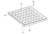
図3は、直下型のバックライトモジュール40の斜視図である。基板58上にLEDユニ
ット30が直列に接続されて、配置されている。また、LEDユニット30の周辺には、
反射シート61が設けられている。なお、図示しないが、LEDユニット30は、コネク
タおよび配線によって、制御回路基板と電気的に接続されている。ここでは、制御回路基
板は、バックライトモジュール40の裏側に配置する。
FIG. 3 is a perspective view of the direct
A
次に、バックライトモジュールの詳細について、図4を用いて説明する。ここでは、図3
に示す破線50のLEDユニットを用いて説明する。
Next, details of the backlight module will be described with reference to FIG. Here, FIG.
It demonstrates using the LED unit of the
配線57が形成される基板58上に、少なくとも赤色波長のピークを有する白色光を発光
するLEDユニット60r、少なくとも緑色波長のピークを有する白色光を発光するLE
Dユニット60g、少なくとも青色波長のピークを有する白色光を発光するLEDユニッ
ト60bを有する。LEDユニット60r、60g、60bはそれぞれ、配線57と導電
性ペースト59で接続されている。基板58及び配線57の露出部上には、反射シート6
1が設けられる。
On the
The
1 is provided.
基板58は、作製工程中の加熱や実際の使用時に生じる発熱に耐えられる基板であれば特
に限定はない。基板58の代表例としては、ガラス基板、プラスチック基板、ガラスエポ
キシ樹脂基板、ポリイミド基板、セラミック基板、アルミナ基板、窒化アルミニウム基板
、プリント基板等がある。あらかじめ、印刷法などで配線が形成されたバックライトモジ
ュール40用のプリント基板を用意すれば、後述する配線57を、蒸着法、スパッタリン
グ法、液滴吐出法(インクジェット法、スクリーン印刷、オフセット印刷等)、または塗
布法などで成膜する必要がないので、歩留まりよく作製することができる。ここでは、基
板58として、ガラスエポキシ樹脂基板を用いる。
The
配線57は、アルミニウム、ニッケル、銅、銀、白金、または金から選ばれた一元素、ま
たは該元素を50%以上含む合金材料で形成される。配線57は、蒸着法、インクジェッ
ト法、印刷法等を用いて形成する。
The
導電性ペースト59は、スズ、銀、ビスマス、銅、インジウム、ニッケル、アンチモン、
亜鉛等を複数含む合金で形成される。
The
It is formed of an alloy containing a plurality of zinc and the like.
本実施の形態では、導電性ペーストを用いたリフロー工程により、基板58上にLEDユ
ニット60r、60b、60gを実装する。代表的には、基板58上に形成される配線5
7上に導電性ペーストをスクリーン印刷やディスペンスにより塗布し、その上にLEDユ
ニット60r、60b、60gをマウンタにより装着する。その後、250〜350℃に
加熱して、導電性ペーストを加熱溶融し、LEDユニット60r、60b、60gの端子
及び配線57を、電気的及び機械的に接続する。
In the present embodiment, the
A conductive paste is applied onto the surface 7 by screen printing or dispensing, and
なお、導電性ペーストを用いたリフロー工程による実装方法の代わりに、異方性導電接着
材を用い、局所的な圧着により基板58にLEDユニット60r、60b、60gを実装
してもよい。
In place of the mounting method by the reflow process using the conductive paste, the
反射シート61は、光反射塗料である白色顔料を有する基板を用いる。反射シート61の
代表例としては、酸化亜鉛、酸化チタン、炭酸カルシウム、酸化シリコン、窒化ホウ素な
ど無機顔料または有機顔料等の白色塗料が表面に印刷または塗装されたプラスチック、上
記無機顔料または有機顔料等の白色塗料が混合されたプラスチック等があり、当該プラス
チックとしては、PET、ポリエステル、ポリオレフィン等がある。また、蛍光材を含む
発泡性PETを用いることができる。または、反射シート61の代わりに、基板58及び
配線57上に白色ソルダーレジストが塗布されてもよい。反射シート61または白色ソル
ダーレジストにより、LEDチップから発光され、基板側に射出した光を、反射させるこ
とができる。
The
LEDユニット60r、60b、60gは、ここでは、図1(A)に示すLEDユニット
30と同様のLEDユニットを用いることができる。
Here, as the
LEDユニット60r、60g、60bにはそれぞれ、微小光共振器43r、43g、4
3bが設けられる。微小光共振器43r、43g、43bは、それぞれLEDチップから
発光した光を干渉させ、赤色光、緑色光、または青色光を発光させる。微小光共振器43
r、43g、43bの光路長は、赤色光、緑色光、または青色光の波長の光の強度を高め
るように決定される。もちろん、これらの波長に限らず、微小光共振器43r、43g、
43bの光路長は、任意の波長の強度を高める光路長に設定しうる。このため、微小光共
振器43r、43g、43bの厚さはそれぞれ異なる。
The
3b is provided. The minute
The optical path lengths of r, 43g, and 43b are determined so as to increase the intensity of light having a wavelength of red light, green light, or blue light. Of course, the
The
また、図5に示すように、LEDユニット60r、60g、60b及び反射シート61上
に透光性を有する有機樹脂層63を設けてもよい。有機樹脂層63は、凸状の透光性を有
する有機樹脂層37で示した有機樹脂を適宜用いることができる。なお、凸状の透光性を
有する有機樹脂層37及び透光性を有する有機樹脂層63の界面に空気が含まれないよう
に形成する。さらに、凸状の透光性を有する有機樹脂層37から射出される光の輝度を、
透光性を有する有機樹脂層63により均一にするような光屈折率を有する材料であり、且
つ凸状の透光性を有する有機樹脂層37の光屈折率に近いものを選択することが好ましい
。透光性を有する有機樹脂層63は、液滴吐出法、塗布法、スピンコート、ディップなど
の方法で形成する。また、ドクターナイフ、ロールコーター、カーテンコーター、ナイフ
コーター等の器具を用いて形成してもよい。
Moreover, as shown in FIG. 5, you may provide the
It is preferable to select a material having a light refractive index that is made uniform by the
以上に示すLEDユニット及びバックライトモジュールを用いることで、着色層を透過し
た光の色純度を高めることができる。
By using the LED unit and the backlight module described above, the color purity of light transmitted through the colored layer can be increased.
(実施の形態2)
本実施の形態では、実施の形態1で説明したバックライトモジュールを用いた液晶表示装
置について説明する。
(Embodiment 2)
In this embodiment, a liquid crystal display device using the backlight module described in
本実施の形態の液晶表示装置は、パッシブマトリクス表示及びアクティブマトリクス表示
どちらにおいても実施可能である。図6(A)は、アクティブマトリクス表示の液晶表示
装置200の構成を示すブロック図である。
The liquid crystal display device of this embodiment can be implemented in both passive matrix display and active matrix display. FIG. 6A is a block diagram illustrating a configuration of a liquid
図6(A)において、液晶表示装置200は、画像を表示する画素部210と、信号線駆
動回路214と、走査線駆動回路211と、画素部210に光を射出するバックライトモ
ジュール40と、バックライトモジュール40に含まれるLEDユニットに送る信号を制
御するLED制御回路212とを有している。さらには、画像処理回路(画像エンジンな
ど)など液晶表示装置を動作させるために必要な回路を有している。これらはすべて実施
の形態1で説明した制御回路基板に設けられている。また、上記駆動回路、処理回路及び
画像処理回路は、論理回路部と、スイッチ部またはバッファ部とに大別されるが、回路の
構成については詳細を省略する。また、上記回路の一部または全部をIC等の半導体装置
で実装してもよい。
6A, a liquid
画素部210は、液晶パネルに設けられた複数の画素215から構成されている。走査線
駆動回路211は、画素215を駆動するための回路であり、パルス信号である複数の表
示選択信号を出力する機能を有する。また、信号線駆動回路214は、入力された画像信
号を元に表示データ信号を生成し、生成した表示データ信号を出力する機能を有する。さ
らに、出力された表示データ信号は対応する画素に入力される。
The
図6(B)は画素215の回路図を示す。画素215には、画素電極の電位を制御するス
イッチング素子としてトランジスタ(主に薄膜トランジスタ:TFT)が配置されている
。ゲートが走査線219に電気的に接続され、第1の電極が信号線217に電気的に接続
された薄膜トランジスタ221と、第1の電極が薄膜トランジスタ221の第2の電極に
電気的に接続され、第2の電極が一定の電位を供給する配線(容量線ともいう。)に電気
的に接続された容量素子223と、一方の電極(画素電極ともいう。)が薄膜トランジス
タ221の第2の電極及び容量素子223の第1の電極に電気的に接続され、他方の電極
(対向電極ともいう。)が対向電位を供給する配線に電気的に接続された液晶素子225
と、を有する。
FIG. 6B shows a circuit diagram of the
And having.
本明細書中において、液晶パネルは、液晶の光学的変調作用によって光の透過または非透
過を制御することで画像を表示する。なお、液晶の光学的変調作用は、液晶にかかる電界
(横方向の電界、縦方向の電界または斜め方向の電界を含む)によって制御される。
In this specification, a liquid crystal panel displays an image by controlling transmission or non-transmission of light by an optical modulation action of liquid crystal. Note that the optical modulation action of the liquid crystal is controlled by an electric field applied to the liquid crystal (including a horizontal electric field, a vertical electric field, or an oblique electric field).
次に、液晶表示装置200の形態について図7に示す液晶表示装置200の断面図を参照
して説明する。図7(A)は、実施の形態1に示すバックライトモジュール40と、バッ
クライトモジュール40に重畳する散乱板301と、バックライトモジュール40及び散
乱板301に重畳する第1の偏光板303と、バックライトモジュール40、散乱板30
1、及び第1の偏光板303と重畳する液晶パネル305と、バックライトモジュール4
0、散乱板301、第1の偏光板303、及び液晶パネル305に重畳する第2の偏光板
307を有している。なお、図示しないが、バックライトモジュール40の外側に、反射
板を設け、バックライトモジュール40から漏れた光を反射し、液晶パネル305に射出
してもよい。
Next, the form of the liquid
1 and the
0, a
液晶表示装置200を動作させるために必要な回路は、液晶パネル305、及びバックラ
イトモジュール40と接続される。なお、走査線駆動回路211及び信号線駆動回路21
4は、液晶パネル305に設けてもよい。
Circuits necessary for operating the liquid
4 may be provided on the
次に、液晶表示装置200を構成する各部材の詳細について示す。
Next, details of each member constituting the liquid
バックライトモジュール40は、実施の形態1に示したバックライトモジュールを用いる
。実施の形態1に示すバックライトモジュールは、任意の波長の強度を高める光路長を有
する微小光共振器を有するため、LEDユニットから射出される光において、従来の白色
光を射出するLEDユニットより、任意の波長の強度を高めることができる。このため、
当該光が、任意の波長において強度を高めた色を透過する着色層を透過すると、従来より
も透過光の色純度が高まる。このため、本実施の形態に示す表示装置の色再現性を高める
ことができる。
The
When the light passes through a colored layer that transmits a color with increased intensity at an arbitrary wavelength, the color purity of the transmitted light is increased as compared with the conventional case. Therefore, color reproducibility of the display device described in this embodiment can be improved.
散乱板301から射出される光を偏光させる第1の偏光板303は、散乱板301から射
出される光を偏光できれば特に限定はない。市販品でもよく、従来から用いられているも
のを使用することができる。例えば、ポリビニルアルコールなどの高分子で構成されてい
る偏光板を用いることができる。第1の偏光板303は板状のものであってもシート状(
フィルム状)のものであってもよい。さらに、液晶表示装置200を構成する他の部材と
、できる限り光屈折率が同程度のものを使用することが好ましい。
The first
(Film form). Furthermore, it is preferable to use a member having the same optical refractive index as that of the other members constituting the liquid
液晶パネル305は、基板315上にスイッチング素子を有する層(以下、素子層317
と示す。)と、素子層317上に形成された画素電極319と、遮光層335、着色層3
37、保護層339、及び共通電極323を有する対向基板321と、シール材325と
、入射される光を透過または遮断させる液晶327とで構成されている。また、図7には
図示していないが、画素電極319と共通電極323との間の距離(セルギャップ)を一
定に制御するために、スペーサが設けられていている。スペーサとしては、ビーズスペー
サや、絶縁層を選択的にエッチングすることで得られるスペーサ(ポストスペーサ)を用
いることができる。
The
It shows. ), The
37, a
基板315及び対向基板321には、透光性を有するものが好ましく、バリウムホウケイ
酸ガラスやアルミノホウケイ酸ガラスなどのガラス基板、石英基板、液晶表示装置200
及び素子層317の作製工程の処理温度に耐えうる程度の耐熱性を有するプラスチック基
板などを用いることができる。また、基板315及び対向基板321として、第3世代(
550mm×650mm)、第3.5世代(600mm×720mm、または620mm
×750mm)、第4世代(680mm×880mm、または730mm×920mm)
、第5世代(1100mm×1300mm)、第6世代(1500mm×1850mm)
、第7世代(1870mm×2200mm)、第8世代(2200mm×2400mm)
、第9世代(2400mm×2800mm、2450mm×3050mm)、第10世代
(2950mm×3400mm)等のガラス基板を用いることができる。
The
Alternatively, a plastic substrate or the like having heat resistance high enough to withstand the processing temperature in the manufacturing process of the
550mm x 650mm), 3.5th generation (600mm x 720mm, or 620mm)
× 750 mm), 4th generation (680 mm × 880 mm, or 730 mm × 920 mm)
, 5th generation (1100mm x 1300mm), 6th generation (1500mm x 1850mm)
, 7th generation (1870mm x 2200mm), 8th generation (2200mm x 2400mm)
, Glass substrates of the ninth generation (2400 mm × 2800 mm, 2450 mm × 3050 mm), the tenth generation (2950 mm × 3400 mm) and the like can be used.
素子層317に形成されるスイッチング素子の代表例として、トランジスタがある。トラ
ンジスタについては後述するが、トランジスタは、さまざまな状況下でも液晶表示装置と
して機能するために必要な特性(例えば、高温下及び低温下で動作する温度特性)を有す
る半導体をチャネルに有することが好ましい。アモルファスシリコンをチャネル領域に用
いることはできるが、より温度特性のよい半導体の代表例としては、複数の結晶領域を持
つ微結晶シリコンや、ポリシリコン等が好ましい。また、酸化物半導体をチャネル領域に
用いることができ、酸化物半導体としては、In−Ga−Zn−O系酸化物等がある。ま
た、これらの半導体を用いたトランジスタは、バックライトモジュール40の発熱や、外
光からの熱によって高温化する場合でも、しきい値電圧の変動が少なく、信頼性が高いた
め、温度変化の大きな環境下においても高性能に動作する。
A typical example of the switching element formed in the
画素電極319及び共通電極323には、酸化タングステンを含むインジウム酸化物、酸
化タングステンを含むインジウム亜鉛酸化物、酸化チタンを含むインジウム酸化物、酸化
チタンを含むインジウム錫酸化物、インジウム錫酸化物、インジウム亜鉛酸化物、または
酸化シリコンを添加したインジウム錫酸化物等の透光性を有する導電性材料を用いて形成
することができる。
The
遮光層335は、光を反射、または吸収し、遮光性を有する材料を用いる。例えば、黒色
の有機樹脂を用いることができ、感光性または非感光性のポリイミドなどの樹脂材料に、
顔料系の黒色樹脂やカーボンブラック、チタンブラック等を混合させて形成すればよい。
また、遮光性の金属層を用いることもでき、例えばクロム、モリブデン、ニッケル、チタ
ン、コバルト、銅、タングステン、またはアルミニウムなどを用いればよい。
The light-
A pigment black resin, carbon black, titanium black, or the like may be mixed.
Alternatively, a light-blocking metal layer can be used, and for example, chromium, molybdenum, nickel, titanium, cobalt, copper, tungsten, aluminum, or the like may be used.
着色層337は、有彩色の透光性樹脂を用いて形成することができる。有彩色の透光性樹
脂の代表例としては、感光性、非感光性の有機樹脂がある。感光性の有機樹脂層を用いる
とレジストマスク数を削減することができるため、工程が簡略化し好ましい。
The
有彩色は、黒、灰、白などの無彩色を除く色であり、着色層はカラーフィルタとして機能
させるため、その着色された有彩色の光のみを透過する材料で形成される。有彩色として
は、赤色、緑色、青色などを用いることができる。また、シアン、マゼンダ、イエロー(
黄)などを用いてもよい。着色された有彩色の光のみを透過するとは、着色層において透
過する光が、その有彩色の光の波長にピークを有するということである。
The chromatic color is a color excluding achromatic colors such as black, gray, and white, and the colored layer is formed of a material that transmits only the colored chromatic light in order to function as a color filter. As the chromatic color, red, green, blue, or the like can be used. Also, cyan, magenta, yellow (
Yellow) or the like may be used. To transmit only colored chromatic light means that the light transmitted through the colored layer has a peak at the wavelength of the chromatic light.
着色層337は、含ませる着色材料の濃度と光の透過率の関係に考慮して、最適な厚さを
適宜制御するとよい。
The thickness of the
保護層339は、平坦性を有する絶縁層で形成する。保護層339の代表例としては、ア
クリル樹脂、エポキシ樹脂等がある。
The
なお、ここでは、着色層337を対向基板321に設けているが、素子層317に含まれ
る層間絶縁層として着色層を作ることもできる。例えば、層間絶縁層に、カラーフィルタ
層として機能する有彩色の透光性樹脂層を用いればよい。
Note that although the
層間絶縁層を着色層として直接素子基板側に形成する場合、着色層と画素領域の位置あわ
せの誤差問題が生じず、より精密な形成領域の制御ができ、微細なパターンの画素にも対
応することができる。また、層間絶縁層と着色層を同一の絶縁層で兼ねるので、工程簡略
化、低コスト化といった利点もある。
When the interlayer insulating layer is formed directly on the element substrate side as a colored layer, there is no error problem in alignment between the colored layer and the pixel region, the formation region can be controlled more precisely, and the pixel with a fine pattern is also supported. be able to. In addition, since the interlayer insulating layer and the colored layer are also used as the same insulating layer, there are also advantages such as process simplification and cost reduction.
液晶327の光学的変調作用は、液晶327にかかる電界(横方向の電界、縦方向の電界
または斜め方向の電界を含む)によって制御される。液晶327の種類及び液晶素子の駆
動モードとしては、ネマチック液晶、コレステリック液晶、スメクチック液晶、ディスコ
チック液晶、サーモトロピック液晶、リオトロピック液晶、低分子液晶、高分子液晶、強
誘電液晶、反強誘電液晶、主鎖型液晶、側鎖型高分子液晶、プラズマアドレス液晶(PA
LC)、バナナ型液晶、TN(Twisted Nematic)モード、STN(Su
per Twisted Nematic)モード、IPS(In−Plane−Swi
tching)モード、FFS(Fringe Field Switching)モー
ド、MVA(Multi−domain Vertical Alignment)モー
ド、PVA(Patterned Vertical Alignment)、ASV(
Advanced Super View)モード、ASM(Axially Symm
etric aligned Micro−cell)モード、OCB(Optical
Compensated Birefringence)モード、ECB(Elect
rically Controlled Birefringence)モード、FLC
(Ferroelectric Liquid Crystal)モード、AFLC(A
ntiFerroelectric Liquid Crystal)モード、PDLC
(Polymer Dispersed Liquid Crystal)モード、ゲス
トホストモード等を用いることができる。ただし、これに限定されず、液晶素子として様
々なものを用いることができる。また、配向膜を用いてラビング工程を行うことで、液晶
327が配向しやすくなる。
The optical modulation action of the
LC), banana liquid crystal, TN (Twisted Nematic) mode, STN (Su
per Twisted Nematic) mode, IPS (In-Plane-Swi)
tching) mode, FFS (Fringe Field Switching) mode, MVA (Multi-domain Vertical Alignment) mode, PVA (Patterned Vertical Alignment), ASV (
Advanced Super View mode, ASM (Axial Symm)
electric aligned Micro-cell (OCB) mode, OCB (Optical
Compensated Birefringence) mode, ECB (Elect
(regularly controlled birefringence) mode, FLC
(Ferroelectric Liquid Crystal) mode, AFLC (A
ntiFerroelectric Liquid Crystal) mode, PDLC
(Polymer Dispersed Liquid Crystal) mode, guest host mode, and the like can be used. However, the present invention is not limited to this, and various liquid crystal elements can be used. In addition, the
液晶327は、配向膜を必要としないブルー相を示す液晶を用いて形成してもよい。ブル
ー相は液晶相の一つであり、コレステリック液晶を昇温していくと、コレステリック相か
ら等方相へ転移する直前に発現する相である。ブルー相は、狭い温度範囲でしか発現しな
いため、温度範囲を改善するために、カイラル剤を混合させた液晶組成物を用いて液晶層
に適用する。ブルー相を示す液晶とカイラル剤とを含む液晶組成物は、応答速度が10μ
s〜100μsと短く、光学的に等方性であるため配向処理が不要であり、視野角依存性
が小さい。
The
Since it is as short as s to 100 μs and is optically isotropic, no alignment treatment is required, and the viewing angle dependency is small.
シール材325は、液晶327を基板315と対向基板321の間で封止する機能を有す
る。
The
シール材325としては、可視光硬化性、紫外線硬化性または熱硬化性の樹脂を用いるの
が好ましい。代表的なものとして、アクリル樹脂、エポキシ樹脂、アミン樹脂などを用い
ることができる。また、光(代表的には紫外線)重合開始剤、熱硬化剤、フィラー、カッ
プリング剤を含んでもよい。
As the
液晶パネル305から射出される光を偏光させる第2の偏光板307は、液晶パネル30
5から射出される光を偏光できれば特に限定はない。第1の偏光板303と同じものを用
いることができる。また、液晶表示装置200を構成する他の部材と、できる限り光屈折
率が同程度のものを使用することが好ましい。第1の偏光板303のスリットに対して、
第2の偏光板307のスリットが直交するように設ける。第2の偏光板307は、板状の
ものであってもシート状(フィルム状)のものであってもよい。
The second
There is no particular limitation as long as the light emitted from 5 can be polarized. The same material as the first
The slits of the second
以上により、液晶表示装置200を作製することができる。
Through the above steps, the liquid
次に、液晶表示装置200の他の形態として、バックライトモジュール40から射出され
、散乱板301で明るさが均一になった光の正面輝度を向上させる光学部材を、散乱板3
01と第1の偏光板303との間に設けた液晶表示装置300について説明する。
Next, as another embodiment of the liquid
A liquid
図7(B)に液晶表示装置300の断面図を示す。液晶表示装置の画素部の正面輝度を向
上させる光学部材333としては、プリズムシートや、マイクロレンズシートなどの輝度
向上シート(フィルム)があり、液晶パネル305に対してできる限り垂直な光を入射さ
せるための光学部材である。
FIG. 7B is a cross-sectional view of the liquid
バックライトモジュール40及び散乱板301は、図7(A)の液晶表示装置200で説
明したものを適宜用いることができる。輝度向上シート(フィルム)は1つだけ用いても
よいが、複数用いることで、液晶表示装置の画素部の正面輝度を向上させることができる
。その際、輝度向上シート(フィルム)間には、空気が含まれるように配置するだけでよ
い。
As the
また、第1の偏光板303、液晶パネル305、及び第2の偏光板307は、液晶表示装
置200で説明したものを適宜用いることができる。
For the first
散乱板301と光学部材333が接着されたバックライトモジュール40に、液晶表示装
置200で説明した液晶パネル305を重畳させることで、液晶表示装置300を作製す
ることができる。
The liquid
次に、上記液晶表示装置200、300において、バックライトモジュールから射出され
る光の明るさを均一にすることが可能な液晶表示装置について、図8を用いて説明する。
Next, a liquid crystal display device capable of making the brightness of light emitted from the backlight module uniform in the liquid
図8に示す液晶表示装置400は、図5に示すような、平坦化され、且つ透光性を有する
有機樹脂層63を有するバックライトモジュール62を有する。また、バックライトモジ
ュール62、散乱板301、第1の偏光板303、液晶パネル305、及び第2の偏光板
307がそれぞれ透光性を有する接着剤311、313、329、331で接着されてい
る。
A liquid
つまり、液晶表示装置400は、バックライトモジュール62、散乱板301、第1の偏
光板303、液晶パネル305、及び第2の偏光板307がそれぞれ重畳し、且つすべて
が接着され、封止されている。全ての部材が接着された液晶表示装置400は、液晶表示
装置400内において、散乱板301、第1の偏光板303、液晶パネル305、及び第
2の偏光板307と比較して、屈折率の小さい空気を有する層を有さず、各々の光屈折率
の差が小さくなっており、液晶表示装置400内での光の反射が抑制されるため、バック
ライトモジュール62から射出される光を効率良く利用することができる。このことによ
り、LEDユニットの消費電力、さらには表示装置の表示電力を低減させることができる
。
That is, in the liquid
透光性を有する接着剤311、313、329、331は、バックライトモジュール62
と散乱板301と、できる限り光屈折率が同程度のものを使用することが好ましい。例え
ば、透光性を有する接着剤311、313、329、331は、エポキシ樹脂を含む接着
剤、ウレタン樹脂を含む接着剤、またはシリコーン樹脂を含む接着剤などを用いることが
できる。選択する材料に応じて、液滴吐出法、塗布法、スピンコート、ディップなどの方
法で形成する。また、ドクターナイフ、ロールコーター、カーテンコーター、ナイフコー
ター等の器具を用いて形成してもよい。
The light-transmitting
It is preferable to use a
次に、本発明の一態様の液晶表示装置におけるLEDユニットの駆動方法について説明す
る。
Next, a method for driving the LED unit in the liquid crystal display device of one embodiment of the present invention is described.
図9は、バックライトモジュールの上面図である。バックライトモジュール410におい
て、LEDユニット411を常に点灯させておき、液晶パネルの液晶によって光の透過ま
たは非透過を制御することで画像を表示させることは、複雑な発光素子制御回路を必要と
しないため簡便である(図9(A)を参照。)。
FIG. 9 is a top view of the backlight module. In the
しかし、LEDユニットの消費電力は、液晶表示装置におけるすべての消費電力のうち、
大部分を占めると言われる。つまり、LEDユニットを常に点灯させておくことは、消費
電力の観点から好ましくない。
However, the power consumption of the LED unit is the total power consumption of the liquid crystal display device.
It is said to occupy the majority. That is, it is not preferable that the LED unit is always lit from the viewpoint of power consumption.
そこで、本発明の一態様である直下型のバックライトモジュールにおいて、有用なLED
ユニットの駆動方法とて、LEDユニットを複数の領域に分け、表示画像の濃淡に合わせ
て、LEDユニット自体も領域ごとに明暗を付けるローカルディミング(局所的調光)と
いう方法がある。
Therefore, in the direct type backlight module which is one embodiment of the present invention, a useful LED is used.
As a method for driving the unit, there is a method called local dimming (local dimming) in which the LED unit is divided into a plurality of regions, and the LED unit itself is also brightened or darkened according to the density of the display image.
図9(B)に示すバックライトモジュール420は、ローカルディミング状態を示す。画
像の暗い部分に対応する領域のLEDユニット421、422の輝度を下げ、画像の明る
い部分に対応する領域のLEDユニット423の輝度を上げる。この方法でLEDユニッ
トを駆動させることにより、画像のコントラスト比を向上させ、LEDユニット低消費電
力化を可能にすることができる。
The
ここで、液晶パネル305の詳細について説明する。まず、アクティブマトリクス型の液
晶パネルについて、図10を用いて説明する。
Here, details of the
図10(A)は、液晶パネル305の上面図であり、2画素分の画素を示している。
FIG. 10A is a top view of the
図10(A)において、複数の信号線405(ソース電極405aを含む)が互いに平行
(図中上下方向に延伸)かつ互いに離間した状態で配置されている。複数の走査線401
(ゲート電極401aを含む)は、信号線405に略直交する方向(図中左右方向)に延
伸し、かつ互いに離間するように配置されている。複数の信号線は、信号線駆動回路21
4(図6(A)参照)に繋がっており、複数の走査線、及び容量配線403は走査線駆動
回路211(図6(A)参照)に繋がっている。
In FIG. 10A, a plurality of signal lines 405 (including the
The
4 (see FIG. 6A), and the plurality of scan lines and the
また、容量配線403は、複数の走査線401それぞれに隣接する位置に配置されており
、走査線401に平行な方向、つまり、信号線405に略直交する方向(図中左右方向)
に延伸している。容量素子406は、図10(A)の一点破線で囲まれた箇所であり、ゲ
ート絶縁層402を誘電体として、容量配線403とドレイン配線409(ドレイン電極
409aを含む)とで構成されている。画素電極319はドレイン配線409と開口部4
50で電気的に接続されている。
The
Is stretched. The
50 is electrically connected.
画素電極319の電位を制御するトランジスタ430は、図中左上の角に配置されている
。画素電極319及びトランジスタ430は、マトリクス状に複数配置されている。
A
また、図10に示す画素構成に限定されず、容量配線を設けず、画素電極と、隣り合う画
素の走査線とゲート絶縁層及び他の絶縁層を介して重ねて、容量素子を形成してもよい。
この場合、容量配線を省略することができ、画素における開口率を高めることができる。
Further, the present invention is not limited to the pixel configuration shown in FIG. 10, and no capacitor wiring is provided, and a capacitor element is formed by overlapping a pixel electrode and a scan line of an adjacent pixel with a gate insulating layer and another insulating layer interposed therebetween. Also good.
In this case, the capacitor wiring can be omitted, and the aperture ratio in the pixel can be increased.
図10(B)は、図10(A)のA−B間における断面図である。また、図10(B)に
おける分断されている箇所は、図10(A)のA−B間において省略されている箇所であ
る。
FIG. 10B is a cross-sectional view taken along a line AB in FIG. 10B is a portion that is omitted between A and B in FIG. 10A.
ここでは、トランジスタ430の構成について説明する。トランジスタ430は逆スタガ
型の薄膜トランジスタ(TFT)であり、絶縁表面を有する基板である基板315上に形
成され、ゲート電極401a、ゲート絶縁層402、半導体層408、ソース電極405
a及びドレイン電極409aを含む。これらは、所望の成膜工程、所望のフォトリソグラ
フィ工程及び所望のエッチング工程によって作製することができる。
Here, the structure of the
a and the
液晶パネル305に適用できるトランジスタの構造は特に限定されず、例えばトップゲー
ト構造及びボトムゲート構造それぞれのスタガ型及びプレーナ型などを用いることができ
る。また、トランジスタはチャネル形成領域が一つ形成されるシングルゲート構造でも、
2つ形成されるダブルゲート構造もしくは3つ形成されるトリプルゲート構造であっても
よい。また、チャネル領域の上下にゲート絶縁層を介して配置された2つのゲート電極を
有する、デュアルゲート型でもよい。本実施の形態のトランジスタはシングルゲート型で
ある。
There is no particular limitation on the structure of the transistor applicable to the
Two double gate structures or three triple gate structures may be formed. Alternatively, a dual gate type having two gate electrodes arranged above and below the channel region with a gate insulating layer interposed therebetween may be used. The transistor in this embodiment is a single gate type.
トランジスタ430を覆い、半導体層408に接する絶縁層407、絶縁層407上に層
間絶縁層413が積層されている。
An insulating
半導体層408は、上記したように、さまざまな状況下でも液晶表示装置として機能する
ために必要な特性(例えば、高温下でも、低温下でも動作する温度特性)を有する半導体
を用いることが好ましい。アモルファスシリコンを用いることはできるが、より温度特性
のよい半導体の代表例としては、複数の結晶領域を持つ微結晶シリコンや、ポリシリコン
等が好ましい。また、酸化物半導体も用いることができ、酸化物半導体としては、In−
Ga−Zn−O系酸化物等がある。また、これらの半導体を用いたトランジスタ素子は、
バックライトモジュールの発熱や、外光からの熱によって高温化する場合でも、しきい値
電圧の変動が少なく、信頼性が高いため、温度変化の大きな環境下においても高性能に動
作する。
As described above, the
There are Ga—Zn—O-based oxides and the like. In addition, transistor elements using these semiconductors are
Even when the backlight module is heated due to heat generation or heat from outside light, the threshold voltage hardly fluctuates and the reliability is high, so that it operates with high performance even in an environment with a large temperature change.
また、点線で示した容量素子406は、上記したように容量配線403とドレイン電極4
09aの間に誘電体としてゲート絶縁層402が積層されている。容量配線403は、ゲ
ート電極401aと同階層であり、同じ条件で形成されるため、ゲート電極401a形成
時に形成される。つまり、トランジスタ430とは別に容量素子406を作り込む必要な
く、所望のフォトリソグラフィによって、トランジスタ430作製する手順で、容量素子
406も作製することができる。
Further, the
A
基板315と対向基板321とを、液晶327を間に挟持させてシール材325(図7参
照)で固着する。シール材325及び液晶327は、上記したものを用いることができる
。液晶327を形成する方法として、ディスペンサ法(滴下法)や、基板315と対向基
板321とを貼り合わせてから毛細管現象等を用いて液晶を注入する注入法を用いること
ができる。シール材325に紫外線などの光硬化樹脂を用い、滴下法で液晶層を形成する
場合など、高分子安定化処理の光照射工程によってシール材325の硬化も行ってもよい
。
The
また、画素電極319と共通電極323との間の距離(セルギャップ)を一定に制御する
ためにスペーサ415が設けられていている。ここでは、ビーズスペーサを用いているが
、絶縁層を選択的にエッチングすることで得られるスペーサ(ポストスペーサ)を用いて
もよい。液晶327を用いる液晶表示装置において、セルギャップは1μm以上20μm
以下とすることが好ましい。なお、本明細書においてセルギャップの厚さとは、液晶の厚
さ(膜厚)の最大値とする。
In addition, a
The following is preferable. In the present specification, the thickness of the cell gap is the maximum value of the thickness (film thickness) of the liquid crystal.
また、トランジスタ430の半導体層や、コンタクトホールと重畳する領域、または画素
間などに遮光層(ブラックマトリクス)を設ける。また、画素電極に対応する領域に着色
層を設ける。
Further, a light-blocking layer (black matrix) is provided in the semiconductor layer of the
次に、画素内のスイッチング素子(トランジスタ)を有するアクティブマトリクスの液晶
パネル305に比べて、簡易に作製することができるパッシブマトリクス表示の液晶パネ
ル305について、図11を用いて説明する。パッシブマトリクス表示の液晶パネル30
5には、画素内のスイッチング素子(トランジスタ)を設ける必要がないために、簡易に
作製することができる。
Next, a passive matrix display
Since it is not necessary to provide a switching element (transistor) in the pixel, it can be easily manufactured.
図11(A)は、パッシブマトリクス表示の液晶パネル305の上面図である。また、図
11(B)は、図11(A)におけるC−D間の断面図である。また、図11(A)には
、液晶327、遮光層335、着色層337、保護層339、及び対向基板321は省略
され図示されていないが、それぞれ、図11(B)で示すように設けられている。
FIG. 11A is a top view of a
対向基板321と基板315との間には、共通電極1706a、1706b、1706c
、絶縁層1707、及び画素電極1701a、1701b、1701cが設けられている
。画素電極1701a、1701b、1701cは、アクティブマトリクス表示の画素電
極319(図7参照。)に相当し、共通電極1706a、1706b、1706cは、ア
クティブマトリクス表示の共通電極323(図7参照)に相当する。さらに、画素電極1
701a、1701b、1701cは、アクティブマトリクス表示の走査線駆動回路に相
当するコモンドライバで制御され、共通電極1706a、1706b、1706cは、ア
クティブマトリクス表示の信号線駆動回路に相当するセグメントドライバで制御される。
Between the
In addition, an insulating
画素電極1701a、1701b、1701c、及び共通電極1706a、1706b、
1706cは開口パターンを有する形状であり、液晶素子の画素領域において長方形の開
口(スリット)を有している。
画素電極1701a、1701b、1701cと共通電極1706a、1706b、17
06cとの間に電界を形成することで、液晶327を制御する。液晶には水平方向の電界
が形成されるため、その電界を用いて液晶分子を制御できる。液晶分子を基板と平行な方
向で制御できるため、視野角が広くなる。
The
また、対向基板321に遮光層335、着色層337、及び保護層339を有する。
In addition, the
図示していないが、上記アクティブマトリクス表示と同様に、セルギャップを保つために
、上記スペーサを用いることができ、液晶327を封止するために上記シール材料を用い
ることができる。
Although not shown, the spacer can be used to maintain the cell gap as in the active matrix display, and the sealing material can be used to seal the
なお、本実施の形態は、他の実施の形態と自由に組み合わせることができる。 Note that this embodiment can be freely combined with any of the other embodiments.
(実施の形態3)
本実施の形態では、MEMS(Micro Electro Mechanical S
ystems)を用いて各画素におけるバックライトからの光の透過量を制御する表示装
置について、図12乃至図14を用いて説明する。
(Embodiment 3)
In the present embodiment, MEMS (Micro Electro Mechanical S) is used.
A display device that controls the amount of light transmitted from the backlight in each pixel using (systems) will be described with reference to FIGS.
図12は、三次元的な立体構造を有し、一部が可動する(即ち、移動可能な)微小構造体
であるMEMSを用いて、各画素におけるバックライトからの光の透過量を制御する表示
装置500の断面図である。
FIG. 12 illustrates the amount of light transmitted from the backlight in each pixel by using a MEMS that is a microstructure having a three-dimensional structure and a part of which is movable (that is, movable). 3 is a cross-sectional view of a
第1の基板501上には、反射層503が形成される。反射層503上には、透光性を有
する絶縁層505が設けられる。透光性を有する絶縁層505上には、MEMSスイッチ
507r、507g、507bが形成される。なお、図示しないが、透光性を有する絶縁
層505は複数の絶縁層で構成され、当該絶縁層の間にMEMSスイッチ507r、50
7g、507bに接続するトランジスタがそれぞれ形成される。当該トランジスタは、実
施の形態2に示すトランジスタを適宜用いることができる。第1の基板501に対向する
第2の基板511は、反射層503に対向する位置に遮光層513が形成され、反射層5
03で囲われた開口部503r、503g、503bそれぞれに対向する位置に着色層5
14r、514g、514bを有する。なお、着色層514rは、赤色光を透過し、着色
層514gは、緑色光を透過し、着色層514bは、青色光を透過する。
A
Transistors connected to 7g and 507b are formed. As the transistor, the transistor described in
The colored layer 5 is located at a position facing each of the
14r, 514g, 514b. Note that the
また、第1の基板501側から順に、散乱板515、輝度向上シート517、及びバック
ライト519を有する。または、第1の基板501側から順に、輝度向上シート517、
散乱板515、及びバックライト519を有してもよい。第1の基板501及び散乱板5
15、散乱板515及び輝度向上シート517、輝度向上シート517及びバックライト
519はそれぞれ、透光性を有する接着剤521、523、525で固着されている。
In addition, a
A
15, the
また、第2の基板511から、バックライト519を覆うように、メタルシートまたは成
型プラスチックを用いた筐体527を有する。
In addition, a
本実施の形態に示す表示装置500は、例えば、反射層503に囲まれた開口部503g
、503bを、MEMSスイッチ507gのシャッタ508gの非開口部、MEMSスイ
ッチ507bのシャッタ508bの非開口部で覆うことで、バックライト519からの光
をシャッタ508g、508bの非開口部で反射し、バックライト519からの光を透過
しない。また、MEMSスイッチ507rのシャッタ508rは、反射層503に囲まれ
た開口部503rを覆わず、反射層503上に移動する。このため、バックライト519
からの光は開口部503rにおいて透過し、着色層の色(ここでは、赤色。)の光が射出
される。
In the
, 503b is covered with the non-opening portion of the
The light from the light passes through the opening 503r, and light of the color of the colored layer (here, red) is emitted.
また、MEMSスイッチ507の開閉回数またはデューティー比により、各画素の輝度や
階調を制御することができる。
In addition, the luminance and gradation of each pixel can be controlled by the number of times of opening / closing the MEMS switch 507 or the duty ratio.
第1の基板501、第2の基板511は、実施の形態2に示す液晶表示装置に用いる基板
と同様の基板を適宜用いることができる。
As the
反射層503は、アルミニウム、銀、モリブデン、タングステン、ニッケル、クロム、及
びこれらの合金、並びにAgPdCu合金等を用いて形成する。反射層503の厚さは、
30nm以上1000nmとする。開口部の形状は、矩形、円形、楕円形、多角形等にす
ることができる。開口部503r、503g、503bは、バックライト519から射出
された光を表示装置の外側へ透過する。なお、反射層503は、バックライト519から
射出された光で、開口部を透過しなかった光を反射し、バックライトモジュールで再度反
射することで、反射光を再利用することができる。
The
30 nm to 1000 nm. The shape of the opening can be rectangular, circular, elliptical, polygonal, or the like. The
反射層503は、スパッタリング法、蒸着法等で成膜した後、フォトリソグラフィ工程に
より一部をエッチングすることで形成することができる。または、反射層503は、印刷
法、インクジェット法等を用いて形成することができる。
The
透光性を有する絶縁層505は、酸化シリコン、窒化シリコン、酸化窒化シリコン、窒化
酸化シリコン等をスパッタリング法、CVD法、蒸着法等で形成する。
The light-transmitting
MEMSスイッチ507r、507g、507bはそれぞれ同じ構造である。ここでは、
MEMSスイッチ507rを代表例に用いて、図12及び図13を用いて説明する。
The MEMS switches 507r, 507g, and 507b have the same structure. here,
The
図13は、MEMSスイッチ507rの斜視図である。MEMSスイッチ507rは、ア
クチュエータ541に結合されたシャッタ543を有する。シャッタ543には開口部が
設けられる。アクチュエータ541は、2つの柔軟性を有するアクチュエータ545を有
する。シャッタ543の一方の辺は、アクチュエータ545に接続されている。アクチュ
エータ545は、シャッタ543を、絶縁層505表面に平行な横方向に移動させる機能
を有する。
FIG. 13 is a perspective view of the
アクチュエータ545は、シャッタ543及び構造体549に接続する可動電極551と
、構造体553に接続する可動電極555とを有する。可動電極555は、可動電極55
1に隣接しており、可動電極555の一端は構造体553に接続し、他端は自由に動くこ
とができる。また、可動電極555の自由に動くことが可能な端部は、可動電極551及
び構造体549の接続部に最も近くなるように、湾曲している。
The
1, one end of the
シャッタ543の他方の辺は、アクチュエータ541によって及ぼされた力に対抗する復
元力を有する、スプリング547に接続されている。スプリング547は、構造体557
に接続されている。
The other side of the
It is connected to the.
構造体549、553、557は、シャッタ543、アクチュエータ545、及びスプリ
ング547を、絶縁層505の表面の近傍において、浮遊させる機械的支持体として機能
する。
The
シャッタ543の下方には、反射層で囲まれる開口部559が設けられる。開口部559
は、図12の開口部503rに相当する。
An
Corresponds to the opening 503r in FIG.
MEMSスイッチ507rに含まれる構造体553は、図示しないトランジスタと接続す
る。このため、構造体553に接続される可動電極555に、トランジスタを介して任意
の電圧を印加することができる。また、構造体549、557は、それぞれ図12に示す
反射層503を介して接地電極(GND)と接続する。このため、構造体549に接続す
る可動電極551及び構造体557に接続するスプリング547の電位は、GNDとなっ
ている。なお、構造体549、557は、任意の電圧を印加できる共通電極に電気的に接
続されてもよい。
The
可動電極555に電圧が印加されると、可動電極551との間の電位差により、可動電極
551及び可動電極555が電気的に引き寄せあう。この結果、可動電極551に接続す
るシャッタ543が、構造体553の方へ引きよせられ、構造体553の方へ横方向に移
動する。可動電極551はスプリングとして働くため、可動電極551及び可動電極55
5との電位間の電圧が除去された場合に、可動電極551は、可動電極551に蓄積され
た応力を解放しながら、シャッタ543をその初期位置に押し戻す。
When a voltage is applied to the
5 is removed, the
MEMSスイッチ507rの作製方法について、以下に説明する。絶縁層505上にフォ
トリソグラフィ工程により所定の形状を有する犠牲層を形成する。犠牲層としては、ポリ
イミド、アクリル等の有機樹脂、酸化シリコン、窒化シリコン、酸化窒化シリコン、窒化
酸化シリコン等の無機絶縁層等で形成することができる。
A method for manufacturing the
次に、犠牲層上に印刷法、スパッタリング法、蒸着法等により導電層を形成した後、選択
的にエッチングをしてMEMSスイッチ507を形成する。または、インクジェット法に
よりMEMSスイッチ507を形成する。
Next, after a conductive layer is formed on the sacrificial layer by a printing method, a sputtering method, an evaporation method, or the like, the MEMS switch 507 is formed by selective etching. Alternatively, the MEMS switch 507 is formed by an inkjet method.
次に、犠牲層を除去することで、空間において可動可能なMEMSスイッチ507rを形
成することができる。なお、この後、MEMSスイッチ507rの表面を酸素プラズマ、
熱酸化等で酸化し、酸化膜を形成することが好ましい。または、原子層蒸着法、CVD法
により、MEMSスイッチ507rの表面に、アルミナ、酸化シリコン、窒化シリコン、
酸化窒化シリコン、窒化酸化シリコン、DLC(ダイヤモンドライクカーボン)等の絶縁
膜を形成することが好ましい。当該絶縁膜をMEMSスイッチ507に設けることで、M
EMSスイッチ507の経年劣化を低減することができる。
Next, by removing the sacrificial layer, the
It is preferable to oxidize by thermal oxidation or the like to form an oxide film. Alternatively, alumina, silicon oxide, silicon nitride, and the like are formed on the surface of the
An insulating film such as silicon oxynitride, silicon nitride oxide, or DLC (diamond-like carbon) is preferably formed. By providing the insulating film on the MEMS switch 507, M
Aging deterioration of the EMS switch 507 can be reduced.
MEMSスイッチ507rは、アルミニウム、銅、ニッケル、クロム、チタン、モリブデ
ン、タンタル、ネオジム等の金属または合金で形成することができる。MEMSスイッチ
507は、厚さ100nm以上5μm以下で形成する。
The
第2の基板511に設けられる遮光層513は、反射層503を覆うように設けられる。
The
第2の基板511に設けられる着色層514r、514g、514bは、実施の形態2に
示す着色層337と同様に形成することができる。なお、着色層は、適宜他の色を透過す
る着色層を設けることができる。
The colored layers 514r, 514g, and 514b provided for the
なお、図示しないが、第1の基板501及び第2の基板511は、シール材で一定間隔を
保持して固定されている。
Note that although not illustrated, the
図12に示す散乱板515及び輝度向上シート517はそれぞれ、実施の形態2に示す散
乱板301及び輝度向上シートを適宜用いることができる。
As the
バックライト519は、実施の形態1に示すバックライトを用いることができる。
As the
実施の形態1に示すバックライトを用いることで、第2の基板511から射出される光の
色純度が高くなる。このため、表示装置の色再現性を高めることができる。また、MEM
Sスイッチを有する表示装置は、バックライト519から射出された光の光利用効率が高
いため、バックライトの輝度を低くしても、十分高いコントラストを得ることができるた
め、表示装置の消費電力を低減することができる。
By using the backlight described in
Since a display device having an S switch has high light use efficiency of light emitted from the
次に、本実施の形態に示す表示装置の回路図及び動作方法について、図13及び図14を
用いて説明する。
Next, a circuit diagram and an operation method of the display device described in this embodiment will be described with reference to FIGS.
図14は、本実施の形態に示す表示装置の回路図を示す。表示装置600は、走査線駆動
回路601と、信号線駆動回路603と、画素部605とを有する。画素部605には、
走査線駆動回路601に接続する走査線609、及び信号線駆動回路603に接続する信
号線611を有する。また、画素部605には、画素607がマトリクス状に配置されて
いる。走査線駆動回路601は、画素607を駆動するための回路であり、パルス信号で
ある複数の表示選択信号を出力する機能を有する。また、信号線駆動回路603は、入力
された画像信号を元にデータ電圧Vdを生成し、生成したデータ電圧Vdを信号線611
に印加する機能を有する。走査線609にゲートが接続し、信号線611に第1の電極が
接続するトランジスタ613と、トランジスタ613の第2の電極と第1の端子が接続す
るMEMSスイッチ615と、トランジスタ613の第2の電極及びMEMSスイッチ6
15の第1の端子に第1の電極が接続する容量素子617とが、各画素607に設けられ
る。MEMSスイッチ615の第2の端子及び容量素子617の第2の電極は、接地電極
に接続する。
FIG. 14 is a circuit diagram of the display device described in this embodiment. The
A
It has the function to apply to. A
Each
トランジスタ613は、MEMSスイッチ615に印加する電圧を制御する。トランジス
タ613は、実施の形態2に示すトランジスタを用いることができる。また、トランジス
タの代わりに、ダイオードまたはMIM(Metal Insulator Metal
)を用いてもよい。
The
) May be used.
MEMSスイッチ615は、図13に示すMEMSスイッチ507rに相当する。
The
MEMSスイッチ615は、2つの可動電極を有するアクチュエータ、及びシャッタを有
する。また、2つの可動電極はそれぞれ、異なる静電容量を有する。
The
トランジスタ613は、MEMSスイッチ615において、より低い静電容量を有する可
動電極555と構造体553を介して接続する。また、MEMSスイッチ507の可動電
極551は面積の大きいシャッタ543に接続されているため、より高い静電容量を有し
、構造体549を介して、共通電極または接地電極に接続される。スプリング547は、
構造体557を介して、共通電極または接地電極に接続される。
The
The
走査線609に書込電圧Vweを次々に印加し、順にトランジスタ613をオンにする。
また、選択された信号線611にデータ電圧Vdを印加する。オン状態のトランジスタ6
13に接続されるMEMSスイッチ615及び容量素子617には、データ電圧Vdが書
き込まれる。このため、可動電極555とシャッタ543との間では、電位差が生じる。
当該電位差の発生に応じて、シャッタが可動電極555の方へ電気的に引き寄せられ、シ
ャッタが移動し、画素部の開口部とシャッタが重複せず、バックライトからの光が当該開
口部を透過する。
The writing voltage Vwe is applied to the
Further, the data voltage Vd is applied to the selected
The data voltage Vd is written into the
In response to the occurrence of the potential difference, the shutter is electrically drawn toward the
アナログ駆動方式の表示装置においては、各信号線611には、各画素607の所望され
る輝度に対応してデータ電圧Vdが印加される。データ電圧Vdに応じて、MEMSスイ
ッチ615のシャッタの移動量が変化する。シャッタの移動量に応じ、画素部の開口部と
シャッタの開口部との重複面積が異なるため、または画素部の開口部とシャッタが重複し
ないため、当該開口部を透過するバックライトからの光量が異なる。
In the analog drive type display device, a data voltage Vd is applied to each
デジタル駆動方式の表示装置においては、データ電圧Vdは、MEMSスイッチ615の
アクチュエータが作動する電圧(作動しきい値電圧)より低い電圧、または作動しきい値
電圧より高い電圧が印加される。作動しきい値電圧より高いデータ電圧Vdの印加により
、MEMSスイッチ615のシャッタが移動し、画素の開口部においてバックライトから
の光が透過する。
In the digital drive type display device, the data voltage Vd is applied with a voltage lower than the voltage (operation threshold voltage) at which the actuator of the
信号線611に印加された電圧は、書込電圧Vweの印加を停止した後も、画素607の
容量素子617に保持される。容量素子617の電圧は、ビデオフレーム全体が書き込ま
れるまで、または新しいデータが信号線611に書き込まれるまで、実質的に蓄積された
ままになる。このため、書込回数を最小限にすることが可能であり、表示装置の消費電力
を低減することができる。
The voltage applied to the
なお、本実施の形態においては、MEMSスイッチ615に接続するトランジスタが一つ
である回路図を示したが、これに限定されるものではなく、適宜トランジスタを設けるこ
とができる。
Note that although a circuit diagram in which one transistor is connected to the
MEMSスイッチを有する表示装置は、バックライトから射出された光の光利用効率が高
いため、バックライトの輝度を低くしても、十分高いコントラストを得ることができるた
め、表示装置の消費電力を低減することができる。
A display device having a MEMS switch has a high light use efficiency of light emitted from a backlight, and thus a sufficiently high contrast can be obtained even when the luminance of the backlight is lowered, thereby reducing power consumption of the display device. can do.
(実施の形態4)
本発明の一態様である表示装置は、さまざまな電子機器に適用することができる。電子機
器としては、例えば、テレビジョン装置(テレビ、またはテレビジョン受信機ともいう)
などが挙げられる。さらには、屋内でのデジタルサイネージ(Digital Sign
age:電子看板)、PID(Public Information Display
)、電車などの乗り物の車内広告等に適用することができる。特に、本発明の一態様であ
る表示装置は、色純度を向上させることができることため、本発明の一態様である表示装
置を、色再現性を求められる上記電子機器として用いることは有用である。そこで、本発
明の一態様である表示装置を用いた電子機器の一例を、図15に示す。
(Embodiment 4)
The display device which is one embodiment of the present invention can be applied to various electronic devices. As an electronic device, for example, a television device (also referred to as a television or a television receiver)
Etc. Digital signage indoors (Digital Sign)
age: Digital signage), PID (Public Information Display)
), In-car advertisements for vehicles such as trains. In particular, since the display device which is one embodiment of the present invention can improve color purity, it is useful to use the display device which is one embodiment of the present invention as the electronic device for which color reproducibility is required. . Thus, an example of an electronic device using the display device which is one embodiment of the present invention is illustrated in FIG.
図15(A)は、テレビジョン装置の一例を示している。テレビジョン装置1000は、
筐体1001に表示部1002が組み込まれている。表示部1002により、映像を表示
することが可能である。また、ここでは、筐体1004により筐体1001を支持した構
成を示している。さらに、テレビジョン装置1000は、スピーカ1003、操作キー1
005(電源スイッチ、または操作スイッチを含む)、接続端子1006、センサ100
7(力、変位、位置、速度、距離、光、温度、音声、時間、電場、電流、電圧、電力、ま
たは赤外線を測定する機能を含むもの)、マイクロフォン1008等が組み込まれている
。
FIG. 15A illustrates an example of a television set. The
A
005 (including power switch or operation switch),
7 (including a function for measuring force, displacement, position, velocity, distance, light, temperature, sound, time, electric field, current, voltage, power, or infrared), a
テレビジョン装置1000の操作は、操作スイッチや、別体のリモコン操作機1010に
より行うことができる。リモコン操作機1010が備える操作キー1009により、チャ
ンネルや音量の操作を行うことができ、表示部1002に表示される映像を操作すること
ができる。また、リモコン操作機1010に、リモコン操作機1010から出力する情報
を表示する表示部1011を設ける構成としてもよい。
The
なお、テレビジョン装置1000は、受信機やモデムなどを備えた構成とする。受信機に
より一般のテレビ放送の受信を行うことができ、さらにモデムを介して有線または無線に
よる通信ネットワークに接続することにより、一方向(送信者から受信者)または双方向
(送信者と受信者間、あるいは受信者間同士など)の情報通信を行うことも可能である。
Note that the
図15(B)は、デジタルサイネージの一例を示している。例えば、デジタルサイネージ
2000は、2つの筐体2002及び筐体2004から構成されている。筐体2002に
は、表示部2006及び2つのスピーカ2008、2010が備わっている。さらに、デ
ジタルサイネージ2000には、ほかにセンサを設けて、人が近くにいないときは画像が
表示されないなど他の構成を設けてもよい。
FIG. 15B illustrates an example of digital signage. For example, the
本発明の一態様である表示装置は、テレビジョン装置1000における表示部1002、
及びデジタルサイネージ2000における表示部2006に用いることができ、色純度を
向上させることができる特徴を有することから、テレビジョン装置1000及びデジタル
サイネージ2000自体の色再現性を高めることができる。
A display device which is one embodiment of the present invention includes a
In addition, since it can be used for the
なお、本実施の形態は、他の実施の形態と自由に組み合わせることができる。 Note that this embodiment can be freely combined with any of the other embodiments.
Claims (4)
バックライトと、有し
前記第1の基板上に、第1の反射層を有し、
前記第1の反射層上に、複数の絶縁層を有し、
前記複数の絶縁層上に、MEMSスイッチを有し、
前記複数の絶縁層の間に、トランジスタを有し、
前記MEMSスイッチは、前記バックライトからの光の透過量を制御する機能を有し、
前記MEMSスイッチは、前記トランジスタと電気的に接続され、
前記トランジスタは、チャネル形成領域を有し、
前記チャネル形成領域は、酸化物半導体を有し、
前記バックライトは、第2の基板と、発光素子ユニットとを有し、
前記発光素子ユニットは、
第3の基板と、
前記第3の基板上に配置された、発光素子チップと、微小光共振器と、
前記発光素子チップ及び前記微小光共振器を覆う蛍光体層と、
を有し、
前記微小光共振器は、
第2の反射層と、
前記第2の反射層上の、透光性を有する層と、
前記透光性を有する層上の、半透過型反射層と、
を有し、
前記微小光共振器は、前記発光素子チップの周辺に配置され、
前記微小光共振器は、特定の発光スペクトルの波長の強度を高める機能を有することを特徴とする表示装置。 A first substrate;
A backlight, and a first reflective layer on the first substrate;
A plurality of insulating layers on the first reflective layer;
A MEMS switch on the plurality of insulating layers;
A transistor between the plurality of insulating layers;
The MEMS switch has a function of controlling the amount of light transmitted from the backlight,
The MEMS switch is electrically connected to the transistor;
The transistor has a channel formation region,
The channel forming region, have a oxide semiconductor,
The backlight includes a second substrate and a light emitting element unit,
The light emitting element unit is:
A third substrate;
A light emitting element chip, a micro optical resonator, and a micro optical resonator disposed on the third substrate;
A phosphor layer covering the light emitting element chip and the minute optical resonator;
Have
The micro-optical resonator is
A second reflective layer;
A translucent layer on the second reflective layer;
A transflective reflective layer on the translucent layer;
Have
The micro optical resonator is disposed around the light emitting element chip,
The micro-optical resonator, a display device characterized in that it have the function of increasing the intensity of the wavelength of a particular emission spectrum.
バックライトと、有し
前記第1の基板の一方の面上に、第1の反射層を有し、
前記第1の反射層上に、複数の絶縁層を有し、
前記複数の絶縁層上に、MEMSスイッチを有し、
前記複数の絶縁層の間に、トランジスタを有し、
前記第1の基板の一方の面と対向する他方の面上に、前記バックライトを有し、
前記MEMSスイッチは、前記バックライトからの光の透過量を制御する機能を有し、
前記MEMSスイッチは、前記トランジスタと電気的に接続され、
前記トランジスタは、チャネル形成領域を有し、
前記チャネル形成領域は、酸化物半導体を有し、
前記バックライトは、第2の基板と、発光素子ユニットとを有し、
前記発光素子ユニットは、
第3の基板と、
前記第3の基板上に配置された、発光素子チップと、微小光共振器と、
前記発光素子チップ及び前記微小光共振器を覆う蛍光体層と、
を有し、
前記微小光共振器は、
第2の反射層と、
前記第2の反射層上の、透光性を有する層と、
前記透光性を有する層上の、半透過型反射層と、
を有し、
前記微小光共振器は、前記発光素子チップの周辺に配置され、
前記微小光共振器は、特定の発光スペクトルの波長の強度を高める機能を有することを特徴とする表示装置。 A first substrate;
A backlight, having a first reflective layer on one surface of the first substrate,
A plurality of insulating layers on the first reflective layer;
A MEMS switch on the plurality of insulating layers;
A transistor between the plurality of insulating layers;
On the other surface facing one surface of the first substrate, the backlight is provided,
The MEMS switch has a function of controlling the amount of light transmitted from the backlight,
The MEMS switch is electrically connected to the transistor;
The transistor has a channel formation region,
The channel forming region, have a oxide semiconductor,
The backlight includes a second substrate and a light emitting element unit,
The light emitting element unit is:
A third substrate;
A light emitting element chip, a micro optical resonator, and a micro optical resonator disposed on the third substrate;
A phosphor layer covering the light emitting element chip and the minute optical resonator;
Have
The micro-optical resonator is
A second reflective layer;
A translucent layer on the second reflective layer;
A transflective reflective layer on the translucent layer;
Have
The micro optical resonator is disposed around the light emitting element chip,
The micro-optical resonator, a display device characterized in that it have the function of increasing the intensity of the wavelength of a particular emission spectrum.
バックライトと、を有し
前記第1の基板の一方の面上に、第1の反射層を有し、
前記第1の反射層上に、複数の絶縁層を有し、
前記複数の絶縁層上に、MEMSスイッチを有し、
前記複数の絶縁層の間に、トランジスタを有し、
前記第1の基板の一方の面と対向する他方の面上に、散乱板を有し、
前記散乱板上に、輝度向上シートを有し、
前記輝度向上シート上に、前記バックライトを有し、
前記MEMSスイッチは、前記バックライトからの光の透過量を制御する機能を有し、
前記MEMSスイッチは、前記トランジスタと電気的に接続され、
前記トランジスタは、チャネル形成領域を有し、
前記チャネル形成領域は、酸化物半導体を有し、
前記バックライトは、第2の基板と、発光素子ユニットとを有し、
前記発光素子ユニットは、
第3の基板と、
前記第3の基板上に配置された、発光素子チップと、微小光共振器と、
前記発光素子チップ及び前記微小光共振器を覆う蛍光体層と、
を有し、
前記微小光共振器は、
第2の反射層と、
前記第2の反射層上の、透光性を有する層と、
前記透光性を有する層上の、半透過型反射層と、
を有し、
前記微小光共振器は、前記発光素子チップの周辺に配置され、
前記微小光共振器は、特定の発光スペクトルの波長の強度を高める機能を有することを特徴とする表示装置。 A first substrate;
A backlight, and a first reflective layer on one surface of the first substrate,
A plurality of insulating layers on the first reflective layer;
A MEMS switch on the plurality of insulating layers;
A transistor between the plurality of insulating layers;
A scattering plate is provided on the other surface facing one surface of the first substrate,
On the scattering plate, having a brightness enhancement sheet,
On the brightness enhancement sheet, having the backlight,
The MEMS switch has a function of controlling the amount of light transmitted from the backlight,
The MEMS switch is electrically connected to the transistor;
The transistor has a channel formation region,
The channel forming region, have a oxide semiconductor,
The backlight includes a second substrate and a light emitting element unit,
The light emitting element unit is:
A third substrate;
A light emitting element chip, a micro optical resonator, and a micro optical resonator disposed on the third substrate;
A phosphor layer covering the light emitting element chip and the minute optical resonator;
Have
The micro-optical resonator is
A second reflective layer;
A translucent layer on the second reflective layer;
A transflective reflective layer on the translucent layer;
Have
The micro optical resonator is disposed around the light emitting element chip,
The micro-optical resonator, a display device characterized in that it have the function of increasing the intensity of the wavelength of a particular emission spectrum.
前記酸化物半導体は、Inと、Gaと、Znと、を有することを特徴とする表示装置。 In any one of Claims 1 thru | or 3,
The display device, wherein the oxide semiconductor includes In, Ga, and Zn.
Applications Claiming Priority (2)
| Application Number | Priority Date | Filing Date | Title |
|---|---|---|---|
| JP2010238723 | 2010-10-25 | ||
| JP2010238723 | 2010-10-25 |
Related Parent Applications (1)
| Application Number | Title | Priority Date | Filing Date |
|---|---|---|---|
| JP2011229456A Division JP5877992B2 (en) | 2010-10-25 | 2011-10-19 | Display device |
Related Child Applications (1)
| Application Number | Title | Priority Date | Filing Date |
|---|---|---|---|
| JP2017084377A Division JP6371437B2 (en) | 2010-10-25 | 2017-04-21 | Light emitting element unit |
Publications (2)
| Publication Number | Publication Date |
|---|---|
| JP2016075959A JP2016075959A (en) | 2016-05-12 |
| JP6134400B2 true JP6134400B2 (en) | 2017-05-24 |
Family
ID=45972748
Family Applications (3)
| Application Number | Title | Priority Date | Filing Date |
|---|---|---|---|
| JP2011229456A Expired - Fee Related JP5877992B2 (en) | 2010-10-25 | 2011-10-19 | Display device |
| JP2016012963A Expired - Fee Related JP6134400B2 (en) | 2010-10-25 | 2016-01-27 | Display device |
| JP2017084377A Active JP6371437B2 (en) | 2010-10-25 | 2017-04-21 | Light emitting element unit |
Family Applications Before (1)
| Application Number | Title | Priority Date | Filing Date |
|---|---|---|---|
| JP2011229456A Expired - Fee Related JP5877992B2 (en) | 2010-10-25 | 2011-10-19 | Display device |
Family Applications After (1)
| Application Number | Title | Priority Date | Filing Date |
|---|---|---|---|
| JP2017084377A Active JP6371437B2 (en) | 2010-10-25 | 2017-04-21 | Light emitting element unit |
Country Status (3)
| Country | Link |
|---|---|
| US (2) | US9306129B2 (en) |
| JP (3) | JP5877992B2 (en) |
| KR (1) | KR20120042691A (en) |
Cited By (1)
| Publication number | Priority date | Publication date | Assignee | Title |
|---|---|---|---|---|
| JP2017168851A (en) * | 2010-10-25 | 2017-09-21 | 株式会社半導体エネルギー研究所 | Light-emitting element unit |
Families Citing this family (26)
| Publication number | Priority date | Publication date | Assignee | Title |
|---|---|---|---|---|
| US8953120B2 (en) | 2011-01-07 | 2015-02-10 | Semiconductor Energy Laboratory Co., Ltd. | Display device |
| KR20120112896A (en) * | 2011-04-04 | 2012-10-12 | 삼성디스플레이 주식회사 | Backlight assembly, method of manufacturing the same and display apparatus having the same |
| US9793444B2 (en) * | 2012-04-06 | 2017-10-17 | Semiconductor Energy Laboratory Co., Ltd. | Display device and electronic device |
| US9711110B2 (en) | 2012-04-06 | 2017-07-18 | Semiconductor Energy Laboratory Co., Ltd. | Display device comprising grayscale conversion portion and display portion |
| TWI611215B (en) | 2012-05-09 | 2018-01-11 | 半導體能源研究所股份有限公司 | Display device and electronic device |
| TWI588540B (en) | 2012-05-09 | 2017-06-21 | 半導體能源研究所股份有限公司 | Display device and electronic device |
| KR102135352B1 (en) * | 2013-08-20 | 2020-07-17 | 엘지전자 주식회사 | Display |
| JP2015118272A (en) * | 2013-12-18 | 2015-06-25 | 株式会社 オルタステクノロジー | Liquid crystal display device for head-up display device, and head-up display device |
| US9541794B2 (en) | 2014-01-10 | 2017-01-10 | Apple Inc. | High dynamic range liquid crystal display |
| JP6250575B2 (en) * | 2015-03-06 | 2017-12-20 | 富士フイルム株式会社 | Backlight unit and image display device |
| KR102373329B1 (en) * | 2015-04-30 | 2022-03-11 | 삼성디스플레이 주식회사 | Organic light emitting diode display |
| KR102377794B1 (en) * | 2015-07-06 | 2022-03-23 | 엘지전자 주식회사 | Display device using semiconductor light emitting device and method for manufacturing |
| KR102396325B1 (en) * | 2015-10-12 | 2022-05-13 | 삼성전자주식회사 | Optical element of led display apparatus and led display apparatus |
| TWI574087B (en) * | 2016-06-21 | 2017-03-11 | 鴻海精密工業股份有限公司 | Light source module and backlight module |
| WO2019138722A1 (en) | 2018-01-12 | 2019-07-18 | 富士フイルム株式会社 | Backlight unit and liquid crystal display |
| KR102105125B1 (en) * | 2018-06-27 | 2020-05-29 | 한국광기술원 | A stretchable patches with double printing wiring structure and a stretchable patch manufacturing method with double printing wiring structure |
| CN109148505B (en) * | 2018-08-23 | 2022-04-29 | 京东方科技集团股份有限公司 | Top-emitting Mircro LED display panel and manufacturing method thereof |
| CN110867507B (en) * | 2018-08-28 | 2021-10-08 | 隆达电子股份有限公司 | Light emitting device and backlight module |
| DE102018126113A1 (en) * | 2018-10-19 | 2020-04-23 | Osram Opto Semiconductors Gmbh | Colored light cell for imaging unit with primary color selection thanks to the oscillating component |
| KR20200118266A (en) * | 2019-04-03 | 2020-10-15 | 삼성디스플레이 주식회사 | Display apparatus and method of manufacturing the same |
| US11428987B2 (en) | 2020-05-22 | 2022-08-30 | Apple Inc. | Electronic device display with a backlight having light-emitting diodes and driver integrated circuits in an active area |
| TWI756061B (en) * | 2021-02-22 | 2022-02-21 | 友達光電股份有限公司 | Display device |
| CN113078190B (en) * | 2021-03-19 | 2022-08-23 | 厦门天马微电子有限公司 | Display panel and display device |
| CN114156306B (en) * | 2021-11-30 | 2023-07-25 | 深圳市华星光电半导体显示技术有限公司 | Display panel manufacturing method, display panel and display device |
| WO2023190475A1 (en) * | 2022-03-30 | 2023-10-05 | 太陽ホールディングス株式会社 | Mounting substrate, connection structure, and electronic component |
| TWI824770B (en) | 2022-10-13 | 2023-12-01 | 財團法人工業技術研究院 | Display element and projector |
Family Cites Families (63)
| Publication number | Priority date | Publication date | Assignee | Title |
|---|---|---|---|---|
| JPS60247622A (en) | 1984-05-23 | 1985-12-07 | Oki Electric Ind Co Ltd | Liquid crystal display device |
| JPH01160063A (en) * | 1987-12-16 | 1989-06-22 | Fujitsu Ltd | Light-emitting element |
| JPH08262438A (en) | 1995-03-23 | 1996-10-11 | Alps Electric Co Ltd | Back light structure for liquid crystal display device |
| JPH0992909A (en) | 1995-09-21 | 1997-04-04 | Casio Comput Co Ltd | Switching device, manufacture of switching device, and display using the switching device |
| US5813753A (en) * | 1997-05-27 | 1998-09-29 | Philips Electronics North America Corporation | UV/blue led-phosphor device with efficient conversion of UV/blues light to visible light |
| US5813752A (en) * | 1997-05-27 | 1998-09-29 | Philips Electronics North America Corporation | UV/blue LED-phosphor device with short wave pass, long wave pass band pass and peroit filters |
| JP2004295141A (en) | 1997-11-20 | 2004-10-21 | Sanyo Electric Co Ltd | Liquid crystal display device |
| US6304304B1 (en) | 1997-11-20 | 2001-10-16 | Sanyo Electric Co., Ltd. | Liquid crystal display having an off driving voltage greater than either zero or an optical characteristics changing voltage |
| JPH11174994A (en) | 1997-12-11 | 1999-07-02 | Sharp Corp | Display device |
| US6037719A (en) | 1998-04-09 | 2000-03-14 | Hughes Electronics Corporation | Matrix-addressed display having micromachined electromechanical switches |
| JP3865942B2 (en) | 1998-07-17 | 2007-01-10 | 富士フイルムホールディングス株式会社 | Active matrix element, light emitting element using the active matrix element, light modulation element, light detection element, exposure element, display device |
| JP3590283B2 (en) | 1999-01-13 | 2004-11-17 | 日本電信電話株式会社 | Manufacturing method of electrostatic movable contact element |
| TW459275B (en) | 1999-07-06 | 2001-10-11 | Semiconductor Energy Lab | Semiconductor device and method of fabricating the same |
| JP3185793B2 (en) | 1999-07-19 | 2001-07-11 | 松下電器産業株式会社 | Liquid crystal display device |
| US6583915B1 (en) | 1999-10-08 | 2003-06-24 | Lg. Philips Lcd Co., Ltd. | Display device using a micro light modulator and fabricating method thereof |
| KR100634831B1 (en) | 1999-12-04 | 2006-10-17 | 엘지.필립스 엘시디 주식회사 | Transparent Type Display Device Using Micro Light Modulator |
| JP2002082652A (en) | 2000-05-18 | 2002-03-22 | Canon Inc | Image display device and method |
| US6998281B2 (en) * | 2000-10-12 | 2006-02-14 | General Electric Company | Solid state lighting device with reduced form factor including LED with directional emission and package with microoptics |
| US20030080839A1 (en) | 2001-10-31 | 2003-05-01 | Wong Marvin Glenn | Method for improving the power handling capacity of MEMS switches |
| US20040031670A1 (en) | 2001-10-31 | 2004-02-19 | Wong Marvin Glenn | Method of actuating a high power micromachined switch |
| JP4164562B2 (en) * | 2002-09-11 | 2008-10-15 | 独立行政法人科学技術振興機構 | Transparent thin film field effect transistor using homologous thin film as active layer |
| US6657525B1 (en) | 2002-05-31 | 2003-12-02 | Northrop Grumman Corporation | Microelectromechanical RF switch |
| TWI351548B (en) | 2003-01-15 | 2011-11-01 | Semiconductor Energy Lab | Manufacturing method of liquid crystal display dev |
| JP4408044B2 (en) | 2003-01-15 | 2010-02-03 | 株式会社半導体エネルギー研究所 | Method for manufacturing liquid crystal display device |
| US7502392B2 (en) | 2003-09-12 | 2009-03-10 | Semiconductor Energy Laboratory Co., Ltd. | Laser oscillator |
| CN102856390B (en) * | 2004-03-12 | 2015-11-25 | 独立行政法人科学技术振兴机构 | Comprise the LCD of thin-film transistor or the transition components of OLED display |
| JP4712413B2 (en) | 2004-04-19 | 2011-06-29 | シチズンホールディングス株式会社 | Variable optical attenuator and optical filter having the same |
| JP2005311153A (en) * | 2004-04-23 | 2005-11-04 | Harison Toshiba Lighting Corp | Envelope for light-emitting element |
| US7416977B2 (en) | 2004-04-28 | 2008-08-26 | Semiconductor Energy Laboratory Co., Ltd. | Method for manufacturing display device, liquid crystal television, and EL television |
| US7985677B2 (en) | 2004-11-30 | 2011-07-26 | Semiconductor Energy Laboratory Co., Ltd. | Method of manufacturing semiconductor device |
| CA2817936A1 (en) | 2005-02-23 | 2006-08-31 | Pixtronix, Inc. | A display utilizing a control matrix to control movement of mems-based light modulators |
| US7304785B2 (en) * | 2005-02-23 | 2007-12-04 | Pixtronix, Inc. | Display methods and apparatus |
| US7271945B2 (en) | 2005-02-23 | 2007-09-18 | Pixtronix, Inc. | Methods and apparatus for actuating displays |
| DE602006003737D1 (en) * | 2005-02-23 | 2009-01-02 | Pixtronix Inc | LIGHT MODULATOR AND METHOD FOR THE PRODUCTION THEREOF |
| JP2006351808A (en) * | 2005-06-15 | 2006-12-28 | Matsushita Electric Works Ltd | Light emitting device |
| TWI261378B (en) * | 2005-09-19 | 2006-09-01 | Ind Tech Res Inst | Polarized light emitting device |
| DE102005062514A1 (en) * | 2005-09-28 | 2007-03-29 | Osram Opto Semiconductors Gmbh | Multi-purpose light emitting diode incorporates selective wavelength trap |
| US8043950B2 (en) | 2005-10-26 | 2011-10-25 | Semiconductor Energy Laboratory Co., Ltd. | Semiconductor device and manufacturing method thereof |
| JP2007165029A (en) * | 2005-12-12 | 2007-06-28 | Hitachi Displays Ltd | Display device |
| JP2007180329A (en) * | 2005-12-28 | 2007-07-12 | Toshiba Lighting & Technology Corp | Light-emitting diode lighting device |
| US7741687B2 (en) | 2006-03-10 | 2010-06-22 | Semiconductor Energy Laboratory Co., Ltd. | Microstructure, semiconductor device, and manufacturing method of the microstructure |
| JP2007273562A (en) | 2006-03-30 | 2007-10-18 | Toshiba Corp | Semiconductor light-emitting device |
| JP2007279480A (en) | 2006-04-10 | 2007-10-25 | Hitachi Displays Ltd | Liquid crystal display device |
| KR101416512B1 (en) | 2006-05-18 | 2014-07-08 | 가부시키가이샤 한도오따이 에네루기 켄큐쇼 | Microstructure, micromachine, and manufacturing method of microstructure and micromachine |
| US7876489B2 (en) | 2006-06-05 | 2011-01-25 | Pixtronix, Inc. | Display apparatus with optical cavities |
| JP2008004645A (en) * | 2006-06-20 | 2008-01-10 | Harison Toshiba Lighting Corp | Light emitting device |
| EP2057693A1 (en) * | 2006-08-29 | 2009-05-13 | Osram-Sylvania Inc. | Enhanced emission from phosphor-converted leds using interferometric filters |
| EP2264507A3 (en) * | 2007-01-19 | 2011-07-20 | Pixtronix Inc. | A display apparatus |
| CN101271869B (en) * | 2007-03-22 | 2015-11-25 | 株式会社半导体能源研究所 | The manufacture method of luminescent device |
| EP1976015B1 (en) | 2007-03-26 | 2014-09-10 | Semiconductor Energy Laboratory Co., Ltd. | Switching element, method for manufacturing the same, and display device including switching element |
| DE102008012316B4 (en) * | 2007-09-28 | 2023-02-02 | OSRAM Opto Semiconductors Gesellschaft mit beschränkter Haftung | Semiconductor light source with a primary radiation source and a luminescence conversion element |
| JP5210901B2 (en) | 2008-02-06 | 2013-06-12 | 株式会社半導体エネルギー研究所 | Liquid crystal display |
| JP2009224245A (en) * | 2008-03-18 | 2009-10-01 | Sony Corp | Light emitting fixture and liquid crystal display device |
| CN102007608B (en) | 2008-05-27 | 2012-11-14 | 夏普株式会社 | Led light source device, backlight device and liquid crystal display device |
| JP2010040976A (en) * | 2008-08-08 | 2010-02-18 | Sony Corp | Light-emitting element, and lighting device and display device using the same |
| JP2010062067A (en) * | 2008-09-05 | 2010-03-18 | Sony Corp | Method of manufacturing display device, and display device |
| RU2473938C1 (en) * | 2009-01-27 | 2013-01-27 | Шарп Кабусики Кайся | Lc display |
| US8461582B2 (en) * | 2009-03-05 | 2013-06-11 | Semiconductor Energy Laboratory Co., Ltd. | Semiconductor device and method for manufacturing the same |
| WO2011025173A2 (en) | 2009-08-27 | 2011-03-03 | Lg Electronics Inc. | Backlight unit and display device |
| JP2011059149A (en) | 2009-09-07 | 2011-03-24 | Hitachi Displays Ltd | Electronic device |
| TWI531088B (en) * | 2009-11-13 | 2016-04-21 | 首爾偉傲世有限公司 | Light emitting diode chip having distributed bragg reflector |
| JP2012033633A (en) * | 2010-07-29 | 2012-02-16 | Fujifilm Corp | Light-emitting device |
| JP5877992B2 (en) * | 2010-10-25 | 2016-03-08 | 株式会社半導体エネルギー研究所 | Display device |
-
2011
- 2011-10-19 JP JP2011229456A patent/JP5877992B2/en not_active Expired - Fee Related
- 2011-10-20 US US13/277,417 patent/US9306129B2/en active Active
- 2011-10-24 KR KR1020110108651A patent/KR20120042691A/en active Search and Examination
-
2016
- 2016-01-27 JP JP2016012963A patent/JP6134400B2/en not_active Expired - Fee Related
- 2016-04-01 US US15/088,174 patent/US20160218258A1/en not_active Abandoned
-
2017
- 2017-04-21 JP JP2017084377A patent/JP6371437B2/en active Active
Cited By (1)
| Publication number | Priority date | Publication date | Assignee | Title |
|---|---|---|---|---|
| JP2017168851A (en) * | 2010-10-25 | 2017-09-21 | 株式会社半導体エネルギー研究所 | Light-emitting element unit |
Also Published As
| Publication number | Publication date |
|---|---|
| US9306129B2 (en) | 2016-04-05 |
| JP5877992B2 (en) | 2016-03-08 |
| JP2017168851A (en) | 2017-09-21 |
| KR20120042691A (en) | 2012-05-03 |
| US20160218258A1 (en) | 2016-07-28 |
| US20120099048A1 (en) | 2012-04-26 |
| JP2012109549A (en) | 2012-06-07 |
| JP6371437B2 (en) | 2018-08-08 |
| JP2016075959A (en) | 2016-05-12 |
Similar Documents
| Publication | Publication Date | Title |
|---|---|---|
| JP6371437B2 (en) | Light emitting element unit | |
| US8891051B2 (en) | Backlight and display device | |
| US10983386B2 (en) | Liquid crystal display and manufacturing method thereof | |
| TWI522708B (en) | Liquid crystal display device | |
| TWI571684B (en) | Liquid crystal display device | |
| TWI484255B (en) | Liquid crystal display device | |
| TWI438529B (en) | Display device | |
| TWI529465B (en) | Liquid crystal display device | |
| KR101334045B1 (en) | Display device | |
| US10120234B2 (en) | Liquid crystal display apparatus | |
| WO2011158424A1 (en) | Thin film transistor substrate and liquid crystal display device | |
| WO2018147279A1 (en) | Reflective polarizing layer, wavelength conversion layer, and liquid crystal display device | |
| JP2007206557A (en) | Liquid crystal display device | |
| US9459491B2 (en) | Mirror display device and manufacturing method thereof | |
| WO2013005644A1 (en) | Display device | |
| US11656504B2 (en) | Liquid crystal apparatus and electronic device | |
| JP5222477B2 (en) | Display device | |
| JP2005284139A (en) | Display device and its manufacturing method | |
| JP2005316001A (en) | Liquid crystal display element and projection display apparatus |
Legal Events
| Date | Code | Title | Description |
|---|---|---|---|
| A131 | Notification of reasons for refusal |
Free format text: JAPANESE INTERMEDIATE CODE: A131 Effective date: 20161018 |
|
| A977 | Report on retrieval |
Free format text: JAPANESE INTERMEDIATE CODE: A971007 Effective date: 20161019 |
|
| A521 | Written amendment |
Free format text: JAPANESE INTERMEDIATE CODE: A523 Effective date: 20161209 |
|
| TRDD | Decision of grant or rejection written | ||
| A01 | Written decision to grant a patent or to grant a registration (utility model) |
Free format text: JAPANESE INTERMEDIATE CODE: A01 Effective date: 20170328 |
|
| A61 | First payment of annual fees (during grant procedure) |
Free format text: JAPANESE INTERMEDIATE CODE: A61 Effective date: 20170421 |
|
| R150 | Certificate of patent or registration of utility model |
Ref document number: 6134400 Country of ref document: JP Free format text: JAPANESE INTERMEDIATE CODE: R150 |
|
| R250 | Receipt of annual fees |
Free format text: JAPANESE INTERMEDIATE CODE: R250 |
|
| LAPS | Cancellation because of no payment of annual fees |