JP6127816B2 - Semiconductor integrated circuit device, electronic device, and memory control method - Google Patents
Semiconductor integrated circuit device, electronic device, and memory control method Download PDFInfo
- Publication number
- JP6127816B2 JP6127816B2 JP2013160206A JP2013160206A JP6127816B2 JP 6127816 B2 JP6127816 B2 JP 6127816B2 JP 2013160206 A JP2013160206 A JP 2013160206A JP 2013160206 A JP2013160206 A JP 2013160206A JP 6127816 B2 JP6127816 B2 JP 6127816B2
- Authority
- JP
- Japan
- Prior art keywords
- clock signal
- signal
- circuit
- write address
- read address
- Prior art date
- Legal status (The legal status is an assumption and is not a legal conclusion. Google has not performed a legal analysis and makes no representation as to the accuracy of the status listed.)
- Active
Links
Images


Landscapes
- Manipulation Of Pulses (AREA)
Description
本発明は、メモリーを内蔵する半導体集積回路装置、及び、そのような半導体集積回路装置を用いた電子機器に関する。さらに、本発明は、メモリー制御方法等に関する。 The present invention relates to a semiconductor integrated circuit device incorporating a memory and an electronic apparatus using such a semiconductor integrated circuit device. Furthermore, the present invention relates to a memory control method and the like.
近年における電子機器の高速化に伴って、電子機器において用いられるクロック信号の周波数が高くなりつつあり、電子機器から放射される電磁放射ノイズの増加が問題となっている。そのような電磁放射ノイズを低減するために、SSCG(スプレッド・スペクトラム・クロック・ジェネレーション)方式が開発されている。SSCG方式によれば、クロック信号を周波数変調してクロック信号のスペクトラムを拡散することにより、電磁放射ノイズのピーク成分が低減される。 With the recent increase in the speed of electronic devices, the frequency of clock signals used in electronic devices is increasing, and an increase in electromagnetic radiation noise radiated from electronic devices has become a problem. In order to reduce such electromagnetic radiation noise, an SSCG (Spread Spectrum Clock Generation) system has been developed. According to the SSCG method, the peak component of electromagnetic radiation noise is reduced by frequency-modulating the clock signal to spread the spectrum of the clock signal.
SSCG方式を採用した半導体集積回路装置においては、一定の周波数を有する基準クロック信号に同期して入力されるデータを、変調クロック信号に同期して動作する内部回路に受け渡すために、データのバッファリング及びフロー制御を行うディジタル回路としてFIFO(First In First Out:ファイフォ)が用いられる場合がある。その場合には、基準クロック信号と変調クロック信号との位相差に相当するデータの入出力時間差を、FIFOによって吸収することができる。 In a semiconductor integrated circuit device employing the SSCG method, a data buffer is used to transfer data input in synchronization with a reference clock signal having a constant frequency to an internal circuit operating in synchronization with the modulation clock signal. A FIFO (First In First Out) may be used as a digital circuit for performing ring and flow control. In that case, the input / output time difference of data corresponding to the phase difference between the reference clock signal and the modulation clock signal can be absorbed by the FIFO.
そのために、FIFOにおいては、ライトアドレスカウンターが、基準クロック信号に同期してライトアドレスを生成し、リードアドレスカウンターが、変調クロック信号に同期してリードアドレスを生成する。ここで、アドレスカウンターを定期的に初期化しない場合には、外部からのノイズ等によって一方のアドレスカウンターが誤動作すると、FIFOが誤動作したまま正常動作に復帰することができない。 Therefore, in the FIFO, the write address counter generates a write address in synchronization with the reference clock signal, and the read address counter generates a read address in synchronization with the modulation clock signal. Here, when the address counter is not periodically initialized, if one address counter malfunctions due to external noise or the like, the normal operation cannot be restored while the FIFO malfunctions.
しかしながら、アドレスカウンターを初期化すると、次のような問題が生じる。第1に、ライトアドレスカウンターとリードアドレスカウンターとを初期化して両者の同期をとった瞬間に、データの出力順が崩れてしまう。第2に、アドレスカウンターを初期化した瞬間の取り込みデータが破壊される可能性がある。従って、アドレスカウンターの初期化は、データの無効期間中に行う必要があり、データが連続して入力される場合には、アドレスカウンターの初期化が困難であった。 However, when the address counter is initialized, the following problems occur. First, at the moment when the write address counter and the read address counter are initialized and synchronized with each other, the data output order is lost. Secondly, there is a possibility that captured data at the moment when the address counter is initialized is destroyed. Therefore, it is necessary to initialize the address counter during the invalid period of data, and it is difficult to initialize the address counter when data is continuously input.
関連する技術として、特許文献1には、FIFO等のメモリーにおいて、外部クロック信号に従ってアドレス値を順次指定し、リセット時に特定アドレスに戻す動作を行う半導体記憶装置が開示されている。この半導体記憶装置は、リードクロック信号に同期してデータが読み出されるメモリーと、リードクロック信号に同期して、リードカウンタークロック信号とメモリーリードアクセス信号とを生成し、かつ、リセット信号がアクティブになった後に、リードクロック信号に同期してアクティブとなるリードカウンターリセット信号を生成するリードコントローラーと、リードクロック信号に同期してアドレス値の異なる第1のリードアドレス信号を順次発生し、リードカウンターリセット信号がアクティブの時にリセットされるリードカウンターと、少なくともリードカウンターからの第1のリードアドレス信号と、リセット信号とに基づいて、第2のリードアドレス信号をメモリーに出力するリードアドレス設定回路とを有し、リードアドレス設定回路からの第2のリードアドレス信号のアドレス値は、リセット信号がノンアクティブの時に第1のリードアドレス信号のアドレス値に基づいて設定され、リセット信号がアクティブの時に第1のリードアドレス信号の論理に拘わらず特定アドレス値に設定される。
As a related technique,
特許文献1によれば、リードクロック信号と非同期のリセット信号が外部から供給されると、リードクロック信号に同期してアクティブとなるリードカウンターリセット信号が内部で生成され、リードカウンターリセット信号によってリードカウンターがリセットされる。しかしながら、リードカウンターがリセットされるとアドレス値が変化するので、メモリーから読み出されるデータの連続性が損なわれてしまう。
According to
そこで、上記の点に鑑み、本発明の目的の1つは、SSCG方式を採用した半導体集積回路装置において、入力データのバッファリングを行うメモリーを、外部からのノイズ等による誤動作から正常動作に復帰させると共に、メモリーが誤動作していない場合には、メモリーから読み出されるデータの連続性を維持することである。 Accordingly, in view of the above points, one of the objects of the present invention is to restore a memory that performs buffering of input data to a normal operation from a malfunction caused by external noise or the like in a semiconductor integrated circuit device adopting an SSCG method. In addition, when the memory does not malfunction, the continuity of data read from the memory is maintained.
以上の課題を解決するため、本発明の1つの観点に係る半導体集積回路装置は、一定の周波数を有する第1のクロック信号に基づいて、変調された周波数を有する第2のクロック信号を生成する変調回路と、第1又は第2のクロック信号のパルスをカウントすることにより、所定の周期毎にアクティブとなるタイミング信号を生成するタイミング信号生成回路と、タイミング信号がアクティブとなる際に第1のクロック信号と第2のクロック信号との位相差を所定の範囲内にすると共に、上記所定の周期において第2のクロック信号の周波数を変化させるように、変調回路を制御する制御回路と、初期状態において設定された第1の初期値を第1のクロック信号に同期してインクリメントすることにより得られる第1のカウント値に基づいて、ライトアドレスを生成するライトアドレスカウンターと、初期状態において設定された第2の初期値を第2のクロック信号に同期してインクリメントすることにより得られる第2のカウント値に基づいて、リードアドレスを生成するリードアドレスカウンターと、第1のクロック信号に同期して、ライトアドレスによって指定されたセルにデータが書き込まれると共に、第2のクロック信号に同期して、リードアドレスによって指定されたセルからデータが読み出されるメモリーとを具備し、ライトアドレスカウンターとリードアドレスカウンターとの内の一方が、タイミング信号によって、ライトアドレスとリードアドレスとの間隔が初期状態となるように同期化される。
In order to solve the above problems, a semiconductor integrated circuit device according to one aspect of the present invention generates a second clock signal having a modulated frequency based on a first clock signal having a constant frequency. A modulation circuit, a timing signal generation circuit that generates a timing signal that becomes active every predetermined period by counting pulses of the first or second clock signal, and a first signal that is activated when the timing signal becomes active A control circuit that controls the modulation circuit so that the phase difference between the clock signal and the second clock signal is within a predetermined range and the frequency of the second clock signal is changed in the predetermined period; and an initial state Based on the first count value obtained by incrementing the first initial value set in
また、本発明の1つの観点に係るメモリー制御方法は、一定の周波数を有する第1のクロック信号に基づいて、変調された周波数を有する第2のクロック信号を生成するステップ(a)と、第1又は第2のクロック信号のパルスをカウントすることにより、所定の周期毎にアクティブとなるタイミング信号を生成するステップ(b)と、タイミング信号がアクティブとなる際に第1のクロック信号と第2のクロック信号との位相差を所定の範囲内にすると共に、上記所定の周期において第2のクロック信号の周波数を変化させるステップ(c)と、ライトアドレスカウンターを用いて、初期状態において設定された第1の初期値を第1のクロック信号に同期してインクリメントすることにより得られる第1のカウント値に基づいて、ライトアドレスを生成するステップ(d)と、リードアドレスカウンターを用いて、初期状態において設定された第2の初期値を第2のクロック信号に同期してインクリメントすることにより得られる第2のカウント値に基づいて、リードアドレスを生成するステップ(e)と、ライトアドレスカウンターとリードアドレスカウンターとの内の一方を、タイミング信号によって、ライトアドレスとリードアドレスとの間隔が初期状態となるように同期化するステップ(f)と、メモリーにおいて、第1のクロック信号に同期して、ライトアドレスによって指定されたセルにデータを書き込むと共に、第2のクロック信号に同期して、リードアドレスによって指定されたセルからデータを読み出すステップ(g)とを具備する。 The memory control method according to one aspect of the present invention includes a step (a) of generating a second clock signal having a modulated frequency based on a first clock signal having a constant frequency; (B) generating a timing signal that becomes active every predetermined period by counting the pulses of the first or second clock signal, and the first clock signal and the second when the timing signal becomes active The phase difference between the first clock signal and the second clock signal is set within the predetermined range and the frequency of the second clock signal is changed in the predetermined cycle, and the initial value is set using the write address counter. Based on the first count value obtained by incrementing the first initial value in synchronization with the first clock signal, the write-in Step (d) of generating a response to the second count value obtained by incrementing the second initial value set in the initial state in synchronization with the second clock signal using the read address counter Based on the step (e) for generating the read address, one of the write address counter and the read address counter is synchronized with the timing signal so that the interval between the write address and the read address becomes the initial state. In step (f), in the memory, data is written to the cell specified by the write address in synchronization with the first clock signal, and from the cell specified by the read address in synchronization with the second clock signal. Reading data (g).
本発明の1つの観点によれば、ライトアドレスカウンターとリードアドレスカウンターとの内の一方を、タイミング信号によって、ライトアドレスとリードアドレスとの間隔が初期状態となるように定期的に同期化することにより、SSCG方式を採用した半導体集積回路装置において入力データのバッファリングを行うメモリーを、外部からのノイズ等による誤動作から正常動作に復帰させることができる。また、タイミング信号がアクティブとなる際には、第1及び第2のクロック信号の位相が揃っているので、メモリーが誤動作していない場合には、メモリーから読み出されるデータの連続性を維持することができる。従って、データの有効期間/無効期間に関わらずアドレスカウンターの同期化を行うことが可能であり、データの無効期間が存在しないアプリケーションにも本発明を適用することができる。 According to one aspect of the present invention, one of the write address counter and the read address counter is periodically synchronized with the timing signal so that the interval between the write address and the read address is in an initial state. Thus, in the semiconductor integrated circuit device adopting the SSCG method, the memory for buffering the input data can be returned to the normal operation from the malfunction due to external noise or the like. In addition, when the timing signal becomes active, the phases of the first and second clock signals are aligned, so that the continuity of data read from the memory is maintained when the memory is not malfunctioning. Can do. Therefore, it is possible to synchronize the address counter regardless of the valid / invalid period of data, and the present invention can be applied to an application in which there is no invalid period of data.
ここで、ライトアドレスカウンターが、タイミング信号によって同期化されたときに、リードアドレスの値に基づいて第1のカウント値を設定し、その後、第1のカウント値を第1のクロック信号に同期してインクリメントすることにより、ライトアドレスを生成しても良い。あるいは、リードアドレスカウンターが、タイミング信号によって同期化されたときに、ライトアドレスの値に基づいて第2のカウント値を設定し、その後、第2のカウント値を第2のクロック信号に同期してインクリメントすることにより、リードアドレスを生成しても良い。これにより、メモリーが誤動作している場合には、ライトアドレスとリードアドレスとの間隔を初期状態に復帰させることができる。 Here, when the write address counter is synchronized by the timing signal, the first count value is set based on the value of the read address, and then the first count value is synchronized with the first clock signal. The write address may be generated by incrementing the address. Alternatively, when the read address counter is synchronized with the timing signal, the second count value is set based on the value of the write address, and then the second count value is synchronized with the second clock signal. The read address may be generated by incrementing. Thereby, when the memory is malfunctioning, the interval between the write address and the read address can be returned to the initial state.
以上において、変調回路が、第1のクロック信号に基づいて、複数の異なる位相を有する多相クロック信号を出力する遅延回路と、選択信号に従って多相クロック信号の内の1つを選択することにより、第2のクロック信号を生成する選択回路とを含み、制御回路が、タイミング信号がアクティブとなる際に第1のクロック信号と第2のクロック信号との位相差を所定の範囲内にすると共に、所定の周期において第2のクロック信号の周波数を変化させるように、選択信号を生成するようにしても良い。これにより、簡単な回路構成で、第2のクロック信号を確実に生成することができる。 In the above, the modulation circuit outputs a multiphase clock signal having a plurality of different phases based on the first clock signal, and selects one of the multiphase clock signals according to the selection signal. A selection circuit that generates a second clock signal, and the control circuit sets the phase difference between the first clock signal and the second clock signal within a predetermined range when the timing signal becomes active. The selection signal may be generated so that the frequency of the second clock signal is changed in a predetermined cycle. Thus, the second clock signal can be reliably generated with a simple circuit configuration.
また、半導体集積回路装置が、第2のクロック信号の生成が停止したときに内部リセット信号をアクティブにするクロック停止検出回路をさらに具備し、タイミング信号生成回路が、内部リセット信号によってリセットされるようにしても良い。これにより、第2のクロック信号の生成が停止するとタイミング信号生成回路がリセットされるので、再びタイミング信号が生成されるようになる。 The semiconductor integrated circuit device further includes a clock stop detection circuit that activates the internal reset signal when the generation of the second clock signal stops, so that the timing signal generation circuit is reset by the internal reset signal. Anyway. Accordingly, when the generation of the second clock signal is stopped, the timing signal generation circuit is reset, so that the timing signal is generated again.
さらに、本発明の1つの観点に係る電子機器は、上記いずれかの半導体集積回路装置を具備する。これにより、携帯電話や液晶テレビ等の電子機器において、SSCG方式を採用した半導体集積回路装置に入力されるデータのバッファリングを行うメモリーの誤動作を防止することができる。 Furthermore, an electronic apparatus according to one aspect of the present invention includes any one of the above semiconductor integrated circuit devices. Thereby, in an electronic device such as a mobile phone or a liquid crystal television, it is possible to prevent malfunction of a memory that buffers data input to a semiconductor integrated circuit device adopting the SSCG method.
以下、本発明の実施形態について、図面を参照しながら詳しく説明する。なお、同一の構成要素には同一の参照符号を付して、重複する説明を省略する。
図1は、本発明の第1の実施形態に係る半導体集積回路装置の構成例を示すブロック図である。この半導体集積回路装置は、クロック信号のスペクトラムを拡散することによって電磁放射ノイズを低減するSSCG方式を採用しており、例えば、携帯電話や液晶テレビ等の電子機器に搭載されて、液晶表示パネルを駆動するために用いられる。
Hereinafter, embodiments of the present invention will be described in detail with reference to the drawings. In addition, the same referential mark is attached | subjected to the same component and the overlapping description is abbreviate | omitted.
FIG. 1 is a block diagram showing a configuration example of a semiconductor integrated circuit device according to the first embodiment of the present invention. This semiconductor integrated circuit device employs an SSCG method that reduces electromagnetic radiation noise by diffusing the spectrum of a clock signal. For example, the semiconductor integrated circuit device is mounted on an electronic device such as a mobile phone or a liquid crystal television to display a liquid crystal display panel. Used to drive.
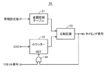
図1に示すように、この半導体集積回路装置は、クロック信号生成回路10と、変調回路20と、クロック停止検出回路30と、論理回路40と、タイミング信号生成回路50と、制御回路60と、FIFO70と、機能ブロック80と、同期化ブロック90と、ドライバー回路100と、複数の入力端子及び出力端子とを含んでいる。
As shown in FIG. 1, the semiconductor integrated circuit device includes a clock
クロック信号生成回路10は、水晶振動子等を用いて、一定の周波数を有する第1のクロック信号(以下、「基準クロック信号」ともいう)CK1を生成する。なお、クロック信号生成回路10を半導体集積回路装置内に設けず、外部からクロック信号入力端子CLKに基準クロック信号CK1を入力するようにしても良い。
The clock
変調回路20〜制御回路60は、SSCG回路ブロック(SSマクロ)を構成している。変調回路20は、基準クロック信号CK1を周波数変調することにより、一定の周波数を有する基準クロック信号CK1に基づいて、変調された周波数を有する第2のクロック信号(以下、「変調クロック信号」ともいう)CK2を生成する。変調回路20は、ディジタル回路で構成しても良いし、アナログ回路で構成しても良い。
The
クロック停止検出回路30は、変調回路20による変調クロック信号CK2の生成が停止したときに、内部リセット信号をアクティブにする。クロック停止検出回路30から出力される内部リセット信号、及び、外部リセット信号入力端子RSTに入力される外部リセット信号がハイアクティブである場合には、論理回路40として、例えば、図1に示すOR回路が用いられる。
The clock
論理回路40は、内部リセット信号と外部リセット信号との論理和を求め、それらの論理和を表すリセット信号をタイミング信号生成回路50及び制御回路60に出力する。従って、タイミング信号生成回路50及び制御回路60は、変調回路20による変調クロック信号CK2の生成が停止したとき、及び、パワーオンリセット等によって外部リセット信号がアクティブになったときに、リセットされることになる。
The
タイミング信号生成回路50は、基準クロック信号CK1又は変調クロック信号CK2のパルスをカウントすることにより、所定の周期(以下においては、「変調周期」ともいう)毎にアクティブとなるタイミング信号を生成する。図1においては、タイミング信号生成回路50が変調クロック信号CK2のパルスをカウントする場合の接続状態が示されている。変調クロック信号CK2の生成が停止するとタイミング信号生成回路50がリセットされて、再びタイミング信号が生成されるようになる。
The timing
制御回路60は、タイミング信号生成回路50によって生成されるタイミング信号がアクティブとなる際に基準クロック信号CK1と変調クロック信号CK2との位相差を所定の範囲内にすると共に、変調周期において変調クロック信号CK2の周波数を変化させるように、変調回路20を制御する。制御回路60は、周期的にアクティブとなるタイミング信号によって一定期間毎に初期化されるので、デッドロックや誤動作から容易に復帰することができる。
The
ここで、所定の範囲とは、例えば、基準クロック信号CK1と変調クロック信号CK2との内のいずれの一方についても他方から位相が360°以上ずれない範囲をいう。本願においては、基準クロック信号CK1と変調クロック信号CK2との位相差が所定の範囲内である場合に、基準クロック信号CK1と変調クロック信号CK2との「位相が揃っている」という表現を用いる。 Here, the predetermined range refers to, for example, a range in which the phase of any one of the reference clock signal CK1 and the modulated clock signal CK2 is not shifted from the other by 360 ° or more. In this application, when the phase difference between the reference clock signal CK1 and the modulation clock signal CK2 is within a predetermined range, the expression “the phases are aligned” between the reference clock signal CK1 and the modulation clock signal CK2 is used.
一定の周波数を有する基準クロック信号CK1に同期して外部からデータ入力端子DINに入力されるデータ(例えば、画像データ、以降においては、画像データを扱う場合について説明する)を、変調クロック信号CK2に同期して動作する内部回路に受け渡すために、画像データのバッファリング及びフロー制御を行う必要がある。そのために、本実施形態においては、FIFO70が設けられている。
Data that is externally input to the data input terminal DIN in synchronization with the reference clock signal CK1 having a certain frequency (for example, image data, and hereinafter, a case where image data is handled) is converted to the modulation clock signal CK2. It is necessary to perform buffering of image data and flow control in order to transfer to an internal circuit that operates in synchronization. Therefore, in this embodiment, a
FIFO70は、ライトアドレスカウンター71と、リードアドレスカウンター72と、画像データのバッファリングを行うメモリーとして、例えば、デュアルポートRAM(ランダムアクセスメモリー)73とを含んでいる。デュアルポートRAM73は、データ書き込み用のポートと、データ読み出し用のポートとを有している。以下においては、デュアルポートRAM73が16ワードの画像データを時系列で格納するために16段の構成を有し、ライトアドレス及びリードアドレスの各々が4ビットであるものとする。
The
ライトアドレスカウンター71は、電源投入時又はリセット時等の初期状態において設定された第1の初期値を、基準クロック信号CK1に同期して1ずつインクリメントすることにより得られる第1のカウント値に基づいて、ライトアドレスWAD[3:0]を生成する。また、リードアドレスカウンター72は、初期状態において設定された第2の初期値を、変調クロック信号CK2に同期して1ずつインクリメントすることにより得られる第2のカウント値に基づいて、リードアドレスRAD[3:0]を生成する。
The
ここで、デュアルポートRAM73が16段の構成を有する場合に、第1の初期値を「0」に設定し、第2の初期値を「8」に設定しても良い。その場合には、ライトアドレスWAD[3:0]とリードアドレスRAD[3:0]との間隔が、デュアルポートRAM73の段数の半分の値である「8」となるので、変調クロック信号CK2の位相の進み及び遅れに対して余裕が得られる。
Here, when the
デュアルポートRAM73には、データ入力端子DINに入力される画像データがライトデータWDTとして供給され、基準クロック信号CK1がライトクロック信号WCKとして供給される。デュアルポートRAM73は、基準クロック信号CK1に同期して、ライトアドレスWAD[3:0]によって指定されたセルに画像データを書き込む。
Image data input to the data input terminal DIN is supplied to the
また、デュアルポートRAM73には、変調クロック信号CK2がリードクロック信号RCKとして供給される。デュアルポートRAM73は、変調クロック信号CK2に同期して、リードアドレスRAD[3:0]によって指定されたセルから、リードデータRDTとして画像データを読み出す。
Further, the modulation clock signal CK2 is supplied to the
第1の実施形態においては、リードアドレスカウンター72が、タイミング信号生成回路50によって生成されるタイミング信号によって、ライトアドレスWAD[3:0]とリードアドレスRAD[3:0]との間隔が初期状態となるように同期化される。これにより、ライトアドレスWAD[3:0]を基準として、リードアドレスRAD[3:0]が定期的に再設定されるので、外部からのノイズ等による誤動作からデュアルポートRAM73を正常動作に復帰させることができる。また、タイミング信号がアクティブとなる際には、基準クロック信号CK1及び変調クロック信号CK2の位相が揃っているので、デュアルポートRAM73が誤動作していない場合には、デュアルポートRAM73から読み出される画像データの連続性を維持することができる。
In the first embodiment, the interval between the write address WAD [3: 0] and the read address RAD [3: 0] is set to the initial state by the read
リードアドレスカウンター72は、タイミング信号によって同期化されたときに、ライトアドレスWAD[3:0]の値に基づいて第2のカウント値を設定し、その後、第2のカウント値を変調クロック信号CK2に同期して1ずつインクリメントすることにより、リードアドレスRAD[3:0]を生成しても良い。これにより、デュアルポートRAM73が誤動作している場合には、ライトアドレスWAD[3:0]とリードアドレスRAD[3:0]との間隔を初期状態に復帰させることができる。
When synchronized with the timing signal, the read
例えば、リードアドレスカウンター72は、タイミング信号によって同期化されたときに、ライトアドレスWAD[3:0]の値に第2の初期値と第1の初期値との差を加算することにより、第2のカウント値を設定する。ここで、第1の初期値が「0」で、第2の初期値が「8」である場合には、第2の初期値と第1の初期値との差は「8」となる。
For example, when the read
従って、ライトアドレスWAD[3:0]の値が「0」である場合に、第2のカウント値として「8」が算出され、ライトアドレスWAD[3:0]の値が「1」である場合に、第2のカウント値として「9」が算出される。ただし、算出された値が「16」以上となった場合には、その値から「16」を減算することにより、第2のカウント値が設定される。 Therefore, when the value of the write address WAD [3: 0] is “0”, “8” is calculated as the second count value, and the value of the write address WAD [3: 0] is “1”. In this case, “9” is calculated as the second count value. However, when the calculated value is “16” or more, the second count value is set by subtracting “16” from the value.
機能ブロック80は、変調クロック信号CK2に同期して、デュアルポートRAM73から読み出される画像データを入力し、画像データを処理することにより、画像処理等の機能を実現する。同期化ブロック90は、変調クロック信号CK2に同期して機能ブロック80から入力される画像データを、基準クロック信号CK1に同期して出力する。ドライバー回路100は、基準クロック信号CK1に同期して、同期化ブロック90から入力される画像データに基づいて表示パネルを駆動するための複数の駆動信号を生成し、それらの駆動信号を出力端子S1〜SJにそれぞれ供給する。
The
次に、SSCG回路ブロックを構成する各回路について詳しく説明する。
図2は、図1に示す変調回路の構成例を示すブロック図である。図2に示すように、変調回路20は、遅延回路21と、選択回路22とを含んでいる。遅延回路21は、基準クロック信号CK1に基づいて、複数の異なる位相を有する多相クロック信号を出力する。選択回路22は、選択信号に従って、遅延回路21から出力される多相クロック信号の内の1つを選択することにより、変調された周波数を有する変調クロック信号CK2を生成する。
Next, each circuit constituting the SSCG circuit block will be described in detail.
FIG. 2 is a block diagram showing a configuration example of the modulation circuit shown in FIG. As shown in FIG. 2, the
図1に示す制御回路60は、タイミング信号生成回路50によって生成されるタイミング信号がアクティブとなる際に基準クロック信号CK1と変調クロック信号CK2との位相差を所定の範囲内にすると共に、変調周期において変調クロック信号CK2の周波数を変化させるように、選択信号を生成する。これにより、簡単な回路構成で、変調クロック信号CK2を確実に生成することができる。
The
図3は、図2に示す遅延回路の構成例を示す図である。遅延回路21は、基準クロック信号CK1を入力するバッファー210と、バッファー210から出力されるクロック信号CK(t)をそれぞれの遅延量で順次遅延させる直列接続された複数の遅延素子211、212、・・・とを含んでいる。ここで、バッファー210は、2つのインバーターを直列に接続して構成しても良い。また、各々の遅延素子は、1つのバッファー又は直列接続された複数のバッファーのゲート遅延によって実現しても良い。
FIG. 3 is a diagram showing a configuration example of the delay circuit shown in FIG. The
図3に示すように、第1番目の遅延素子211〜第K番目の遅延素子214における遅延量をΔT1、ΔT2、・・・、ΔTKで表すと(Kは自然数)、時刻tにおいて多相クロック信号CK(t)、CK(t−T1)、CK(t−T2)、・・・、CK(t−TK)が遅延回路21から出力される。ただし、T1=ΔT1、T2=ΔT1+ΔT2、・・・、TK=ΔT1+ΔT2+・・・+ΔTKである。従って、これらの多相クロック信号の内から1つのクロック信号を順次選択することにより、周波数が変化する変調クロック信号を生成することができる。
As shown in FIG. 3, when the delay amounts in the
例えば、ΔT1=ΔT2=・・・=ΔTKのように位相差を等間隔とすれば、次第に位相が遅れるクロック信号CK(t)、CK(t−T1)、CK(t−T2)、・・・を順次選択している期間において、一定の負の周波数偏移を有する周波数変調を実現することができる。一方、次第に位相が早まるクロック信号CK(t−TK)、CK(t−TK−1)、CK(t−TK−2)、・・・を順次選択している期間においては、一定の正の周波数偏移を有する周波数変調を実現することができる。 For example, if the phase differences are equal intervals, such as ΔT 1 = ΔT 2 =... = ΔT K , the clock signals CK (t), CK (t−T 1 ), and CK (t−T) whose phases are gradually delayed. 2 ) In a period in which... Are sequentially selected, frequency modulation having a constant negative frequency shift can be realized. On the other hand, in the period in which the clock signals CK (t−T K ), CK (t−T K−1 ), CK (t−T K−2 ),. A frequency modulation with a positive frequency deviation of can be realized.
あるいは、ΔTを一定の遅延量としたときに、ΔT1+ΔT=ΔT2、ΔT2+ΔT=ΔT3、・・・のように位相差を累積的とすれば、次第に位相が遅れるクロック信号CK(t)、CK(t−T1)、CK(t−T2)、・・・を順次選択している期間において、時間と共に瞬時周波数が線形に減少する周波数変調を実現することができる。一方、次第に位相が早まるクロック信号CK(t−TK)、CK(t−TK−1)、CK(t−TK−2)、・・・を順次選択している期間においては、時間と共に瞬時周波数が線形に増加する周波数変調を実現することができる。 Alternatively, when ΔT is a fixed delay amount, if the phase difference is cumulative such as ΔT 1 + ΔT = ΔT 2 , ΔT 2 + ΔT = ΔT 3 ,..., The clock signal CK ( t), CK (t−T 1 ), CK (t−T 2 ),... can be realized in a frequency modulation in which the instantaneous frequency linearly decreases with time. On the other hand, in the period in which the clock signals CK (t−T K ), CK (t−T K−1 ), CK (t−T K−2 ),. At the same time, frequency modulation in which the instantaneous frequency increases linearly can be realized.
図4は、図3に示す遅延回路から出力される多相クロック信号の選択動作を説明するための図である。ここでは、例として、3つのクロック信号CK(t)、CK(t−T1)、CK(t−T2)を用いる場合について説明する。図3において(1)〜(5)で示すように、これらのクロック信号の内から1つのクロック信号を順次選択することにより、低い瞬時周波数と高い瞬時周波数とを交互に有する変調クロック信号MCK(t)を生成することができる。 FIG. 4 is a diagram for explaining the selection operation of the multiphase clock signal output from the delay circuit shown in FIG. Here, as an example, a case where three clock signals CK (t), CK (t−T 1 ), and CK (t−T 2 ) are used will be described. As indicated by (1) to (5) in FIG. 3, by sequentially selecting one clock signal from these clock signals, a modulated clock signal MCK having alternating low and high instantaneous frequencies ( t) can be generated.
図5は、図1に示すクロック停止検出回路の構成例を示すブロック図である。図5に示すように、クロック停止検出回路30は、カウンター31と、分周回路32と、エッジ検出回路33と、比較回路34と、閾値設定部35とを含んでいる。
FIG. 5 is a block diagram showing a configuration example of the clock stop detection circuit shown in FIG. As shown in FIG. 5, the clock
カウンター31は、複数のDフリップフロップと、EXOR回路やAND回路等の論理回路とによって構成され、カウント値をリセットするために用いられるリセット端子RSTを有している。カウンター31は、基準クロック信号CK1に同期してカウント値を1ずつインクリメントすることにより、基準クロック信号CK1のパルスをカウントしてカウント値を生成し、生成されたカウント値を比較回路34に出力する。
The
分周回路32は、少なくとも1つのDフリップフロップによって構成され、変調クロック信号CK2を所定の分周比で分周し、分周された変調クロック信号(分周信号)を出力する。なお、分周回路32は、変調クロック信号の波形が乱れている場合においても、矩形波に近い波形を有する分周信号を出力することができる。
The
エッジ検出回路33は、例えば、バッファー等によって構成される遅延回路と、遅延回路の入力信号と出力信号との排他的論理和を求めるEXOR回路とによって構成される。エッジ検出回路33は、分周回路32から出力される分周信号のエッジを検出して、分周信号のエッジ部分においてアクティブとなるエッジ検出信号をカウンター31のリセット端子RSTに出力する。このエッジ検出信号によって、カウンター31におけるカウント値がゼロにリセットされる。
The
比較回路34は、カウンター31から出力されるカウント値を閾値設定部35に設定されている閾値と比較して、カウント値が閾値又はそれ以上となったときに、内部リセット信号をアクティブにする。変調クロック信号CK2が生成されている場合には、分周信号がローレベルとハイレベルとの間で遷移するので、エッジ検出信号が周期的にアクティブとなり、カウンター31が周期的にリセットされる。これにより、カウンター31から出力されるカウント値が閾値以上とならないので、比較回路34は内部リセット信号をアクティブにしない。
The
一方、変調クロック信号CK2の生成が停止した場合には、分周信号がローレベル又はハイレベルに固定されて、エッジ検出信号がアクティブとならないので、カウンター31がリセットされなくなる。その結果、カウンター31から出力されるカウント値が次第に増加して閾値と等しくなる。比較回路34は、カウント値が閾値と等しくなったときに、内部リセット信号をアクティブにする。
On the other hand, when the generation of the modulation clock signal CK2 is stopped, the frequency-divided signal is fixed at the low level or the high level, and the edge detection signal is not activated, so that the
図6は、図1に示すタイミング信号生成回路の構成例を示すブロック図である。タイミング信号生成回路50は、変調周期テーブル51と、カウンター52と、比較回路53と、論理回路54とを含んでいる。
FIG. 6 is a block diagram illustrating a configuration example of the timing signal generation circuit illustrated in FIG. The timing
変調周期テーブル51は、レジスター等によって構成される。図1に示すように、半導体集積回路装置は、周期設定信号を入力する入力端子SETを有しており、タイミング信号生成回路50は、入力端子SETに入力される周期設定信号に従って、周期設定値を変調周期テーブル51に格納する。
The modulation period table 51 is configured by a register or the like. As shown in FIG. 1, the semiconductor integrated circuit device has an input terminal SET for inputting a cycle setting signal, and the timing
カウンター52は、複数のDフリップフロップと、EXOR回路やAND回路等の論理回路とによって構成され、カウント値をリセットするために用いられるリセット端子RSTを有している。カウンター52は、変調クロック信号CK2に同期してカウント値を1ずつインクリメントすることにより、変調クロック信号CK2のパルスをカウントする。
The
比較回路53は、カウンター52から出力されるカウント値を、変調周期テーブル51に格納されている設定値と比較することにより、カウント値が設定値又はそれ以上となったときにタイミング信号をアクティブにする。比較回路53から出力されるタイミング信号、及び、論理回路40(図1)から出力されるリセット信号は、論理回路54に入力される。
The
タイミング信号及びリセット信号がハイアクティブである場合には、論理回路54として、例えば、図6に示すOR回路が用いられる。論理回路54は、タイミング信号とリセット信号との論理和を求め、それらの論理和を表す信号をカウンター52のリセット端子RSTに出力する。
When the timing signal and the reset signal are high active, for example, an OR circuit shown in FIG. 6 is used as the
従って、カウンター52は、カウント値が設定値と等しくなったとき、及び、リセット信号がアクティブになったときに、リセットされる。リセット信号がノンアクティブである場合に、タイミング信号生成回路50がパルス状のタイミング信号を生成する周期は、入力端子SET(図1)に入力される周期設定信号に従って設定される。
Accordingly, the
このように、変調クロック信号CK2に基づいてタイミング信号生成回路50を動作させる場合には、選択回路22(図2)が多相クロック信号を選択するタイミングが変調クロック信号CK2に正確に同期するので、選択回路22よって生成される変調クロック信号CK2の波形が乱れるおそれがない。
Thus, when the timing
図1に示す制御回路60は、カウンター又はシフトレジスター等を含んでおり、入力端子SETに入力される周期設定信号に従って、変調クロック信号CK2の周波数を変化させる変調周期を設定する。以下においては、カウンターを用いる場合について説明する。
The
制御回路60は、周期設定信号に従って、第1の閾値〜第3の閾値を設定する。また、制御回路60は、タイミング信号によって初期化され、カウント値をゼロにリセットした後、基準クロック信号CK1又は変調クロック信号CK2のパルスをカウントしてカウント値を生成する。図1においては、制御回路60が変調クロック信号CK2のパルスをカウントする場合の接続状態が示されている。
The
制御回路60は、カウント値がゼロから第1の閾値に達するまでの期間において、図2に示す選択回路22によって選択されるクロック信号の位相が、図3に示すクロック信号CK(t)、CK(t−T1)、CK(t−T2)、・・・、CK(t−TK)のように順次遅れるように選択信号を生成する。
The
また、制御回路60は、カウント値が第1の閾値を超えてから第2の閾値に達するまでの期間において、選択回路22によって選択されるクロック信号の位相が順次進むように選択信号を生成する。さらに、制御回路60は、カウント値が第2の閾値を超えてから第3の閾値に達するまでの期間において、選択回路22によって選択されるクロック信号の位相が順次遅れるように選択信号を生成する。カウント値が第3の閾値に達したら、1変調周期分の変調動作が完了するので、制御回路60は選択信号を初期値に保つ。
In addition, the
図7は、タイミング信号の1パルスと変調クロック信号の周波数との関係を示す図である。選択回路22が、制御回路60によって生成される選択信号に従って多相クロック信号の内の1つを順次選択することにより、変調クロック信号の周波数が図7に示すように変化する。
FIG. 7 is a diagram illustrating the relationship between one pulse of the timing signal and the frequency of the modulated clock signal. The
図7に示す例においては、タイミング信号の1つのパルスに応答して、変調クロック信号の周波数が1変調周期において減少→増加→減少となるように変化する。なお、タイミング信号の1つのパルスに応答して、変調クロック信号の周波数が複数の変調周期において変化するようにしても良い。 In the example shown in FIG. 7, in response to one pulse of the timing signal, the frequency of the modulation clock signal changes so as to decrease → increase → decrease in one modulation period. Note that the frequency of the modulation clock signal may change in a plurality of modulation periods in response to one pulse of the timing signal.
変調クロック信号の中心周波数f0は、基準クロック信号の周波数と等しく、例えば、20MHzである。変調クロック信号の最小周波数f1は、例えば、15MHzであり、変調クロック信号の最大周波数f2は、例えば、25MHzである。変調周期の開始時点及び終了時点においては、変調クロック信号の周波数が基準クロック信号の周波数と等しくなるように設定される。 The center frequency f 0 of the modulated clock signal is equal to the frequency of the reference clock signal, for example, it is 20MHz. The minimum frequency f 1 of the modulation clock signal is, for example, 15 MHz, and the maximum frequency f 2 of the modulation clock signal is, for example, 25 MHz. At the start time and end time of the modulation cycle, the frequency of the modulation clock signal is set to be equal to the frequency of the reference clock signal.
また、変調周期の開始時点においては、変調クロック信号の位相と基準クロック信号の位相とが揃っている。変調クロック信号の周波数が基準クロック信号の周波数よりも小さい期間においては、変調クロック信号の位相(タイミング信号がアクティブになってから第i番目のパルスの位相)が基準クロック信号の位相(タイミング信号がアクティブになってから同じ第i番目のパルスの位相)に対して累積的に遅れて行く。 Also, at the start of the modulation period, the phase of the modulation clock signal and the phase of the reference clock signal are aligned. In a period in which the frequency of the modulation clock signal is smaller than the frequency of the reference clock signal, the phase of the modulation clock signal (the phase of the i-th pulse after the timing signal becomes active) is the phase of the reference clock signal (the timing signal is It becomes cumulatively delayed with respect to the phase of the same i-th pulse after becoming active).
次に、変調クロック信号の周波数が基準クロック信号の周波数よりも大きい期間においては、基準クロック信号の位相に対する変調クロック信号の位相の遅れが次第に解消されて、変調周期の終了時点においては、変調クロック信号の位相と基準クロック信号の位相とが揃うようになる。 Next, in a period in which the frequency of the modulation clock signal is larger than the frequency of the reference clock signal, the phase delay of the modulation clock signal with respect to the phase of the reference clock signal is gradually eliminated, and at the end of the modulation period, the modulation clock signal is The phase of the signal is aligned with the phase of the reference clock signal.
変調クロック信号の位相と基準クロック信号の位相とが揃っている時点においては、変調クロック信号と基準クロック信号とが同期していると考えることができる。従って、ライトアドレスカウンターとリードアドレスカウンターとの内の一方を同期化しても、読み出される画像データの連続性を維持することができる。 When the phase of the modulation clock signal and the phase of the reference clock signal are aligned, it can be considered that the modulation clock signal and the reference clock signal are synchronized. Therefore, even if one of the write address counter and the read address counter is synchronized, the continuity of the read image data can be maintained.
図8は、タイミング信号の複数のパルスと変調クロック信号の周波数との関係を示す図である。タイミング信号生成回路50がタイミング信号を周期的にアクティブにするので、制御回路60は周期的に初期化されることになる。タイミング信号の第1のパルスに応答して変調クロック信号の周波数が第1の変調周期において変化した後に、タイミング信号の第2のパルスに応答して変調クロック信号の周波数が第2の変調周期において変化し、このようにして、変調クロック信号の周波数が連続的に変調される。
FIG. 8 is a diagram illustrating a relationship between a plurality of pulses of the timing signal and the frequency of the modulation clock signal. Since the timing
このように、制御回路60は、複雑な動作を行うのであるが、デッドロックしたり連続的に誤動作したりしても、タイミング信号生成回路50によって周期的にアクティブにされるタイミング信号によって一定期間毎に初期化されるので、一定期間後には必ず正常状態に復帰することができる。一方、タイミング信号を生成するタイミング信号生成回路50は、Dフリップフロップ及び基本的な組み合わせ論理回路のみによって構成される小規模な回路なので、デッドロックや誤動作のおそれが小さいと共に、確実に動作することを容易に証明できる。
As described above, the
ただし、タイミング信号生成回路50が変調クロック信号CK2に同期して動作する場合には、変調クロック信号CK2の生成が停止するとタイミング信号の生成もできなくなる。そこで、変調クロック信号CK2の生成が停止したときに内部リセット信号を生成するクロック停止検出回路30が設けられている。これにより、変調クロック信号CK2の生成が停止するとタイミング信号生成回路50がリセットされるので、再びタイミング信号が生成されるようになる。クロック停止検出回路30も、タイミング信号生成回路50と同様に、Dフリップフロップ及び基本的な組み合わせ論理回路のみによって構成される小規模な回路なので、デッドロックや誤動作のおそれが小さいと共に、確実に動作することを容易に証明できる。
However, when the timing
次に、本発明の第2の実施形態について説明する。
図9は、本発明の第2の実施形態に係る半導体集積回路装置の構成例を示すブロック図である。第2の実施形態においては、ライトアドレスカウンター71が、タイミング信号生成回路50によって生成されるタイミング信号によって、ライトアドレスWAD[3:0]とリードアドレスRAD[3:0]との間隔が初期状態となるように同期化される。これにより、リードアドレスRAD[3:0]を基準としてライトアドレスWAD[3:0]が定期的に再設定されるので、外部からのノイズ等による誤動作からデュアルポートRAM73を正常動作に復帰させることができる。また、タイミング信号がアクティブとなる際には、基準クロック信号CK1及び変調クロック信号CK2の位相が揃っているので、デュアルポートRAM73が誤動作していない場合には、デュアルポートRAM73から読み出される画像データの連続性を維持することができる。
Next, a second embodiment of the present invention will be described.
FIG. 9 is a block diagram showing a configuration example of a semiconductor integrated circuit device according to the second embodiment of the present invention. In the second embodiment, the
ライトアドレスカウンター71は、タイミング信号によって同期化されたときに、リードアドレスRAD[3:0]の値に基づいて第1のカウント値を設定し、その後、第1のカウント値を基準クロック信号CK1に同期して1ずつインクリメントすることにより、ライトアドレスWAD[3:0]を生成しても良い。これにより、FIFO70が誤動作している場合には、ライトアドレスRAD[3:0]とリードアドレスWAD[3:0]との間隔を初期状態に復帰させることができる。
When synchronized with the timing signal, the
例えば、ライトアドレスカウンター71は、タイミング信号によって同期化されたときに、リードアドレスRAD[3:0]の値から第2の初期値と第1の初期値との差を減算することにより、第1のカウント値を設定する。ここで、第1の初期値が「0」で、第2の初期値が「8」である場合には、第2の初期値と第1の初期値との差は「8」となる。
For example, when synchronized with the timing signal, the
具体的には、リードアドレスRAD[3:0]の値が「15」である場合に、第1のカウント値として「7」が算出され、リードアドレスRAD[3:0]の値が「14」である場合に、第1のカウント値として「6」が算出される。ただし、算出された値が「0」未満となった場合には、その値に「16」を加算することにより、第1のカウント値が設定される。その他の点に関しては、第1の実施形態と同様である。 Specifically, when the value of the read address RAD [3: 0] is “15”, “7” is calculated as the first count value, and the value of the read address RAD [3: 0] is “14”. "6" is calculated as the first count value. However, when the calculated value is less than “0”, the first count value is set by adding “16” to the value. The other points are the same as in the first embodiment.
次に、本発明の一実施形態に係るメモリー制御方法について説明する。
図10は、本発明の一実施形態に係るメモリー制御方法を示すフローチャートである。このメモリー制御方法は、図1又は図9に示す半導体集積回路装置において実施することができる。
Next, a memory control method according to an embodiment of the present invention will be described.
FIG. 10 is a flowchart illustrating a memory control method according to an embodiment of the present invention. This memory control method can be implemented in the semiconductor integrated circuit device shown in FIG. 1 or FIG.
図10のステップS1において、変調回路20が、一定の周波数を有する基準クロック信号CK1に基づいて、変調された周波数を有する変調クロック信号CK2を生成する。ステップS2において、タイミング信号生成回路50が、基準クロック信号CK1又は変調クロック信号CK2のパルスをカウントすることにより、所定の周期毎にアクティブとなるタイミング信号を生成する。
In step S1 of FIG. 10, the
ステップS3において、制御回路60が、タイミング信号生成回路50によって生成されるタイミング信号がアクティブとなる際に基準クロック信号CK1と変調クロック信号CK2との位相差を所定の範囲内にすると共に、所定の周期において変調クロック信号CK2の周波数を変化させるように、変調回路20を制御する。
In step S3, the
ステップS4において、ライトアドレスカウンター71が、初期状態において設定された第1の初期値を基準クロック信号CK1に同期して1ずつインクリメントすることにより得られる第1のカウント値に基づいて、ライトアドレスWAD[3:0]を生成する。また、ステップS5において、リードアドレスカウンター72が、初期状態において設定された第2の初期値を、変調クロック信号CK2に同期して1ずつインクリメントすることにより得られる第2のカウント値に基づいて、リードアドレスRAD[3:0]を生成する。
In step S4, the
ステップS6において、タイミング信号生成回路50が、ライトアドレスカウンター71とリードアドレスカウンター72との内の一方を、タイミング信号によって、ライトアドレスWAD[3:0]とリードアドレスRAD[3:0]との間隔が初期状態となるように同期化する。
In step S6, the timing
ステップS7において、デュアルポートRAM73が、基準クロック信号CK1に同期して、ライトアドレスWAD[3:0]によって指定されたセルに画像データを書き込むと共に、変調クロック信号CK2に同期して、リードアドレスRAD[3:0]によって指定されたセルから画像データを読み出す。
In step S7, the
以上の実施形態においては、半導体集積回路装置において画像データの処理を行う例について説明したが、本発明は、この実施形態に限定されるものではなく、一般的なデータの処理を行う場合に適用可能であると共に、当該技術分野において通常の知識を有する者によって、本発明の技術的思想内で多くの変形が可能である。 In the above embodiment, the example in which image data processing is performed in the semiconductor integrated circuit device has been described. However, the present invention is not limited to this embodiment, and is applied to the case of performing general data processing. Many modifications are possible within the technical idea of the present invention by those having ordinary knowledge in the art.
10…クロック信号生成回路、20…変調回路、21…遅延回路、210…バッファー、211〜214…遅延素子、22…選択回路、30…クロック停止検出回路、31…カウンター、32…分周回路、33…エッジ検出回路、34…比較回路、35…閾値設定部、40…論理回路、50…タイミング信号生成回路、51…変調周期テーブル、52…カウンター、53…比較回路、54…論理回路、60…制御回路、70…FIFO、71…ライトアドレスカウンター、72…リードアドレスカウンター、73…デュアルポートRAM、80…機能ブロック、90…同期化ブロック、100…ドライバー回路
DESCRIPTION OF
Claims (8)
所定の周期毎に前記第1のクロック信号と前記第2のクロック信号との位相差を所定の範囲内にすると共に、前記所定の周期において前記第2のクロック信号の周波数を変化させるように、前記変調回路を制御する制御回路と、
初期状態において設定された第1の初期値に基づいて前記第1のクロック信号に同期するライトアドレスを生成するライトアドレスカウンターと、
初期状態において設定された第2の初期値に基づいて前記第2のクロック信号に同期するリードアドレスを生成するリードアドレスカウンターと、
前記第1のクロック信号に同期して、前記ライトアドレスによって指定されたセルにデータが書き込まれると共に、前記第2のクロック信号に同期して、前記リードアドレスによって指定されたセルからデータが読み出されるメモリーと、
を具備し、前記ライトアドレスカウンターと前記リードアドレスカウンターとの内の一方が、前記所定の周期毎に、前記ライトアドレスと前記リードアドレスとの間隔が初期状態となるように同期化される、半導体集積回路装置。 A modulation circuit for generating a second clock signal having a modulated frequency based on a first clock signal having a constant frequency;
A phase difference between the first clock signal and the second clock signal is set within a predetermined range every predetermined cycle, and the frequency of the second clock signal is changed in the predetermined cycle. A control circuit for controlling the modulation circuit;
A write address counter that generates a write address synchronized with the first clock signal based on a first initial value set in an initial state;
A read address counter that generates a read address synchronized with the second clock signal based on a second initial value set in an initial state;
Data is written to the cell specified by the write address in synchronization with the first clock signal, and data is read from the cell specified by the read address in synchronization with the second clock signal. Memory,
And one of the write address counter and the read address counter is synchronized so that an interval between the write address and the read address is in an initial state every predetermined cycle. Integrated circuit device.
前記制御回路は、前記タイミング信号がアクティブとなる際に前記第1のクロック信号と前記第2のクロック信号との位相差を所定の範囲内にすると共に、前記所定の周期において前記第2のクロック信号の周波数を変化させ、
前記ライトアドレスカウンターは、前記第1の初期値を前記第1のクロック信号に同期してインクリメントすることにより得られる第1のカウント値に基づいて、ライトアドレスを生成し、
前記リードアドレスカウンターは、前記第2の初期値を前記第2のクロック信号に同期してインクリメントすることにより得られる第2のカウント値に基づいて、リードアドレスを生成し、
前記ライトアドレスカウンターと前記リードアドレスカウンターとの内の一方は、前記タイミング信号によって同期化される、請求項1記載の半導体集積回路装置。 A timing signal generating circuit that generates a timing signal that becomes active every predetermined period by counting pulses of the first or second clock signal;
The control circuit sets a phase difference between the first clock signal and the second clock signal within a predetermined range when the timing signal becomes active, and the second clock in the predetermined cycle. Change the frequency of the signal,
The write address counter generates a write address based on a first count value obtained by incrementing the first initial value in synchronization with the first clock signal;
The read address counter generates a read address based on a second count value obtained by incrementing the second initial value in synchronization with the second clock signal,
2. The semiconductor integrated circuit device according to claim 1, wherein one of the write address counter and the read address counter is synchronized by the timing signal.
前記第1のクロック信号に基づいて、複数の異なる位相を有する多相クロック信号を出力する遅延回路と、
選択信号に従って前記多相クロック信号の内の1つを選択することにより、前記第2のクロック信号を生成する選択回路と、
を含み、前記制御回路が、前記所定の周期毎に前記第1のクロック信号と前記第2のクロック信号との位相差を所定の範囲内にすると共に、前記所定の周期において前記第2のクロック信号の周波数を変化させるように、前記選択信号を生成する、請求項1〜4のいずれか1項記載の半導体集積回路装置。 The modulation circuit is
A delay circuit that outputs a multi-phase clock signal having a plurality of different phases based on the first clock signal;
A selection circuit for generating the second clock signal by selecting one of the multiphase clock signals according to a selection signal;
And the control circuit sets a phase difference between the first clock signal and the second clock signal within a predetermined range at each predetermined cycle, and the second clock at the predetermined cycle. The semiconductor integrated circuit device according to claim 1, wherein the selection signal is generated so as to change a frequency of the signal.
前記タイミング信号生成回路が、前記内部リセット信号によってリセットされる、
請求項1〜5のいずれか1項記載の半導体集積回路装置。 A clock stop detection circuit for activating an internal reset signal when generation of the second clock signal is stopped;
The timing signal generation circuit is reset by the internal reset signal;
The semiconductor integrated circuit device according to claim 1.
所定の周期毎に前記第1のクロック信号と前記第2のクロック信号との位相差を所定の範囲内にすると共に、前記所定の周期において前記第2のクロック信号の周波数を変化させるステップと、
初期状態において設定された第1の初期値に基づいて前記第1のクロック信号に同期するライトアドレスを生成するステップと、
初期状態において設定された第2の初期値に基づいて前記第2のクロック信号に同期するリードアドレスを生成するステップと、
前記所定の周期毎に、前記ライトアドレスと前記リードアドレスとの間隔が初期状態となるように同期化するステップと、
メモリーにおいて、前記第1のクロック信号に同期して、前記ライトアドレスによって指定されたセルにデータを書き込むと共に、前記第2のクロック信号に同期して、前記リードアドレスによって指定されたセルからデータを読み出すステップと、
を具備するメモリー制御方法。 Generating a second clock signal having a modulated frequency based on a first clock signal having a constant frequency;
Setting a phase difference between the first clock signal and the second clock signal within a predetermined range every predetermined period, and changing a frequency of the second clock signal in the predetermined period;
Generating a write address synchronized with the first clock signal based on a first initial value set in an initial state;
Generating a read address synchronized with the second clock signal based on a second initial value set in an initial state;
Synchronizing the write address and the read address so that the interval between the write address and the read address is in an initial state for each predetermined period;
In the memory, data is written to the cell specified by the write address in synchronization with the first clock signal, and data is read from the cell specified by the read address in synchronization with the second clock signal. A reading step;
A memory control method comprising:
Priority Applications (1)
| Application Number | Priority Date | Filing Date | Title |
|---|---|---|---|
| JP2013160206A JP6127816B2 (en) | 2013-08-01 | 2013-08-01 | Semiconductor integrated circuit device, electronic device, and memory control method |
Applications Claiming Priority (1)
| Application Number | Priority Date | Filing Date | Title |
|---|---|---|---|
| JP2013160206A JP6127816B2 (en) | 2013-08-01 | 2013-08-01 | Semiconductor integrated circuit device, electronic device, and memory control method |
Publications (3)
| Publication Number | Publication Date |
|---|---|
| JP2015032938A JP2015032938A (en) | 2015-02-16 |
| JP2015032938A5 JP2015032938A5 (en) | 2016-05-12 |
| JP6127816B2 true JP6127816B2 (en) | 2017-05-17 |
Family
ID=52517936
Family Applications (1)
| Application Number | Title | Priority Date | Filing Date |
|---|---|---|---|
| JP2013160206A Active JP6127816B2 (en) | 2013-08-01 | 2013-08-01 | Semiconductor integrated circuit device, electronic device, and memory control method |
Country Status (1)
| Country | Link |
|---|---|
| JP (1) | JP6127816B2 (en) |
Family Cites Families (5)
| Publication number | Priority date | Publication date | Assignee | Title |
|---|---|---|---|---|
| JPH0750856B2 (en) * | 1985-12-05 | 1995-05-31 | 日本電気株式会社 | Delay circuit |
| JP3364943B2 (en) * | 1992-02-25 | 2003-01-08 | 株式会社日立製作所 | Clock skew correction circuit |
| JP2001148690A (en) * | 1999-11-19 | 2001-05-29 | Sony Corp | Clock generator |
| JP5177856B2 (en) * | 2008-03-11 | 2013-04-10 | Necエンジニアリング株式会社 | Clock transfer circuit |
| JP5987292B2 (en) * | 2011-10-31 | 2016-09-07 | セイコーエプソン株式会社 | Semiconductor integrated circuit device and electronic apparatus using the same |
-
2013
- 2013-08-01 JP JP2013160206A patent/JP6127816B2/en active Active
Also Published As
| Publication number | Publication date |
|---|---|
| JP2015032938A (en) | 2015-02-16 |
Similar Documents
| Publication | Publication Date | Title |
|---|---|---|
| JP4504581B2 (en) | Register-controlled delay lock loop using ring delay and counter | |
| US7777543B2 (en) | Duty cycle correction circuit apparatus | |
| US7889581B2 (en) | Digital DLL circuit | |
| US9824731B2 (en) | Data reading circuit | |
| CN111161766B (en) | DDR SDRAM physical layer interface circuit and DDR SDRAM control device | |
| US20150015310A1 (en) | Clock delay detecting circuit and semiconductor apparatus using the same | |
| JP4751178B2 (en) | Synchronous semiconductor device | |
| US20080253203A1 (en) | Data output circuit for semiconductor memory apparatus | |
| JP5987292B2 (en) | Semiconductor integrated circuit device and electronic apparatus using the same | |
| CN110442320B (en) | FIFO circuit for double data rate memory system | |
| JP6313085B2 (en) | Semiconductor device | |
| US7392406B2 (en) | Circuit and method for generating clock signals for clocking digital signal processor and memory | |
| JP6127816B2 (en) | Semiconductor integrated circuit device, electronic device, and memory control method | |
| US7696801B2 (en) | Reset method for clock triggering digital circuit and related signal generating apparatus utilizing the reset method | |
| JP2007243601A (en) | Semiconductor integrated circuit | |
| WO2007125519A2 (en) | Latency optimized resynchronization solution for ddr/ddr2 sdram read path | |
| US7427886B2 (en) | Clock generating method and circuit thereof | |
| EP2391007A2 (en) | Division circuit, division device, and electronic apparatus | |
| CN1983446A (en) | Memory controller and its control method | |
| CN112104822B (en) | Imaging device and method of operating the same | |
| US20250015786A1 (en) | Clock doubler, a clock generating device and a semiconductor system using the same | |
| JP2006302056A (en) | Clock control circuit | |
| KR100592188B1 (en) | Data interface device for SDRAM access | |
| US8514005B2 (en) | Circuit and method for generating multiphase clock signals and corresponding indication signals | |
| US11644861B2 (en) | Information processing apparatus including function blocks and generation units |
Legal Events
| Date | Code | Title | Description |
|---|---|---|---|
| RD04 | Notification of resignation of power of attorney |
Free format text: JAPANESE INTERMEDIATE CODE: A7424 Effective date: 20150113 |
|
| A521 | Written amendment |
Free format text: JAPANESE INTERMEDIATE CODE: A523 Effective date: 20160317 |
|
| A621 | Written request for application examination |
Free format text: JAPANESE INTERMEDIATE CODE: A621 Effective date: 20160317 |
|
| RD04 | Notification of resignation of power of attorney |
Free format text: JAPANESE INTERMEDIATE CODE: A7424 Effective date: 20160616 |
|
| RD03 | Notification of appointment of power of attorney |
Free format text: JAPANESE INTERMEDIATE CODE: A7423 Effective date: 20160624 |
|
| A977 | Report on retrieval |
Free format text: JAPANESE INTERMEDIATE CODE: A971007 Effective date: 20161130 |
|
| A131 | Notification of reasons for refusal |
Free format text: JAPANESE INTERMEDIATE CODE: A131 Effective date: 20161213 |
|
| A521 | Written amendment |
Free format text: JAPANESE INTERMEDIATE CODE: A523 Effective date: 20170120 |
|
| TRDD | Decision of grant or rejection written | ||
| A01 | Written decision to grant a patent or to grant a registration (utility model) |
Free format text: JAPANESE INTERMEDIATE CODE: A01 Effective date: 20170314 |
|
| A61 | First payment of annual fees (during grant procedure) |
Free format text: JAPANESE INTERMEDIATE CODE: A61 Effective date: 20170327 |
|
| R150 | Certificate of patent or registration of utility model |
Ref document number: 6127816 Country of ref document: JP Free format text: JAPANESE INTERMEDIATE CODE: R150 |