JP6099372B2 - 半導体装置及び電子機器 - Google Patents
半導体装置及び電子機器 Download PDFInfo
- Publication number
- JP6099372B2 JP6099372B2 JP2012260451A JP2012260451A JP6099372B2 JP 6099372 B2 JP6099372 B2 JP 6099372B2 JP 2012260451 A JP2012260451 A JP 2012260451A JP 2012260451 A JP2012260451 A JP 2012260451A JP 6099372 B2 JP6099372 B2 JP 6099372B2
- Authority
- JP
- Japan
- Prior art keywords
- transistor
- wiring
- potential
- signal
- gate
- Prior art date
- Legal status (The legal status is an assumption and is not a legal conclusion. Google has not performed a legal analysis and makes no representation as to the accuracy of the status listed.)
- Active
Links
Images


Classifications
-
- H—ELECTRICITY
- H10—SEMICONDUCTOR DEVICES; ELECTRIC SOLID-STATE DEVICES NOT OTHERWISE PROVIDED FOR
- H10D—INORGANIC ELECTRIC SEMICONDUCTOR DEVICES
- H10D86/00—Integrated devices formed in or on insulating or conducting substrates, e.g. formed in silicon-on-insulator [SOI] substrates or on stainless steel or glass substrates
- H10D86/40—Integrated devices formed in or on insulating or conducting substrates, e.g. formed in silicon-on-insulator [SOI] substrates or on stainless steel or glass substrates characterised by multiple TFTs
- H10D86/60—Integrated devices formed in or on insulating or conducting substrates, e.g. formed in silicon-on-insulator [SOI] substrates or on stainless steel or glass substrates characterised by multiple TFTs wherein the TFTs are in active matrices
-
- G—PHYSICS
- G11—INFORMATION STORAGE
- G11C—STATIC STORES
- G11C19/00—Digital stores in which the information is moved stepwise, e.g. shift registers
- G11C19/18—Digital stores in which the information is moved stepwise, e.g. shift registers using capacitors as main elements of the stages
- G11C19/182—Digital stores in which the information is moved stepwise, e.g. shift registers using capacitors as main elements of the stages in combination with semiconductor elements, e.g. bipolar transistors, diodes
- G11C19/184—Digital stores in which the information is moved stepwise, e.g. shift registers using capacitors as main elements of the stages in combination with semiconductor elements, e.g. bipolar transistors, diodes with field-effect transistors, e.g. MOS-FET
-
- G—PHYSICS
- G11—INFORMATION STORAGE
- G11C—STATIC STORES
- G11C19/00—Digital stores in which the information is moved stepwise, e.g. shift registers
- G11C19/28—Digital stores in which the information is moved stepwise, e.g. shift registers using semiconductor elements
-
- H—ELECTRICITY
- H10—SEMICONDUCTOR DEVICES; ELECTRIC SOLID-STATE DEVICES NOT OTHERWISE PROVIDED FOR
- H10D—INORGANIC ELECTRIC SEMICONDUCTOR DEVICES
- H10D84/00—Integrated devices formed in or on semiconductor substrates that comprise only semiconducting layers, e.g. on Si wafers or on GaAs-on-Si wafers
- H10D84/80—Integrated devices formed in or on semiconductor substrates that comprise only semiconducting layers, e.g. on Si wafers or on GaAs-on-Si wafers characterised by the integration of at least one component covered by groups H10D12/00 or H10D30/00, e.g. integration of IGFETs
- H10D84/811—Combinations of field-effect devices and one or more diodes, capacitors or resistors
- H10D84/813—Combinations of field-effect devices and capacitor only
-
- H—ELECTRICITY
- H10—SEMICONDUCTOR DEVICES; ELECTRIC SOLID-STATE DEVICES NOT OTHERWISE PROVIDED FOR
- H10D—INORGANIC ELECTRIC SEMICONDUCTOR DEVICES
- H10D86/00—Integrated devices formed in or on insulating or conducting substrates, e.g. formed in silicon-on-insulator [SOI] substrates or on stainless steel or glass substrates
- H10D86/40—Integrated devices formed in or on insulating or conducting substrates, e.g. formed in silicon-on-insulator [SOI] substrates or on stainless steel or glass substrates characterised by multiple TFTs
- H10D86/441—Interconnections, e.g. scanning lines
-
- H—ELECTRICITY
- H10—SEMICONDUCTOR DEVICES; ELECTRIC SOLID-STATE DEVICES NOT OTHERWISE PROVIDED FOR
- H10D—INORGANIC ELECTRIC SEMICONDUCTOR DEVICES
- H10D86/00—Integrated devices formed in or on insulating or conducting substrates, e.g. formed in silicon-on-insulator [SOI] substrates or on stainless steel or glass substrates
- H10D86/40—Integrated devices formed in or on insulating or conducting substrates, e.g. formed in silicon-on-insulator [SOI] substrates or on stainless steel or glass substrates characterised by multiple TFTs
- H10D86/471—Integrated devices formed in or on insulating or conducting substrates, e.g. formed in silicon-on-insulator [SOI] substrates or on stainless steel or glass substrates characterised by multiple TFTs having different architectures, e.g. having both top-gate and bottom-gate TFTs
-
- H—ELECTRICITY
- H10—SEMICONDUCTOR DEVICES; ELECTRIC SOLID-STATE DEVICES NOT OTHERWISE PROVIDED FOR
- H10D—INORGANIC ELECTRIC SEMICONDUCTOR DEVICES
- H10D86/00—Integrated devices formed in or on insulating or conducting substrates, e.g. formed in silicon-on-insulator [SOI] substrates or on stainless steel or glass substrates
- H10D86/40—Integrated devices formed in or on insulating or conducting substrates, e.g. formed in silicon-on-insulator [SOI] substrates or on stainless steel or glass substrates characterised by multiple TFTs
- H10D86/481—Integrated devices formed in or on insulating or conducting substrates, e.g. formed in silicon-on-insulator [SOI] substrates or on stainless steel or glass substrates characterised by multiple TFTs integrated with passive devices, e.g. auxiliary capacitors
-
- G—PHYSICS
- G09—EDUCATION; CRYPTOGRAPHY; DISPLAY; ADVERTISING; SEALS
- G09G—ARRANGEMENTS OR CIRCUITS FOR CONTROL OF INDICATING DEVICES USING STATIC MEANS TO PRESENT VARIABLE INFORMATION
- G09G2310/00—Command of the display device
- G09G2310/02—Addressing, scanning or driving the display screen or processing steps related thereto
- G09G2310/0264—Details of driving circuits
- G09G2310/0267—Details of drivers for scan electrodes, other than drivers for liquid crystal, plasma or OLED displays
-
- G—PHYSICS
- G09—EDUCATION; CRYPTOGRAPHY; DISPLAY; ADVERTISING; SEALS
- G09G—ARRANGEMENTS OR CIRCUITS FOR CONTROL OF INDICATING DEVICES USING STATIC MEANS TO PRESENT VARIABLE INFORMATION
- G09G2310/00—Command of the display device
- G09G2310/02—Addressing, scanning or driving the display screen or processing steps related thereto
- G09G2310/0264—Details of driving circuits
- G09G2310/0286—Details of a shift registers arranged for use in a driving circuit
-
- G—PHYSICS
- G09—EDUCATION; CRYPTOGRAPHY; DISPLAY; ADVERTISING; SEALS
- G09G—ARRANGEMENTS OR CIRCUITS FOR CONTROL OF INDICATING DEVICES USING STATIC MEANS TO PRESENT VARIABLE INFORMATION
- G09G2320/00—Control of display operating conditions
- G09G2320/04—Maintaining the quality of display appearance
- G09G2320/043—Preventing or counteracting the effects of ageing
-
- G—PHYSICS
- G09—EDUCATION; CRYPTOGRAPHY; DISPLAY; ADVERTISING; SEALS
- G09G—ARRANGEMENTS OR CIRCUITS FOR CONTROL OF INDICATING DEVICES USING STATIC MEANS TO PRESENT VARIABLE INFORMATION
- G09G3/00—Control arrangements or circuits, of interest only in connection with visual indicators other than cathode-ray tubes
- G09G3/20—Control arrangements or circuits, of interest only in connection with visual indicators other than cathode-ray tubes for presentation of an assembly of a number of characters, e.g. a page, by composing the assembly by combination of individual elements arranged in a matrix no fixed position being assigned to or needed to be assigned to the individual characters or partial characters
- G09G3/22—Control arrangements or circuits, of interest only in connection with visual indicators other than cathode-ray tubes for presentation of an assembly of a number of characters, e.g. a page, by composing the assembly by combination of individual elements arranged in a matrix no fixed position being assigned to or needed to be assigned to the individual characters or partial characters using controlled light sources
- G09G3/30—Control arrangements or circuits, of interest only in connection with visual indicators other than cathode-ray tubes for presentation of an assembly of a number of characters, e.g. a page, by composing the assembly by combination of individual elements arranged in a matrix no fixed position being assigned to or needed to be assigned to the individual characters or partial characters using controlled light sources using electroluminescent panels
- G09G3/32—Control arrangements or circuits, of interest only in connection with visual indicators other than cathode-ray tubes for presentation of an assembly of a number of characters, e.g. a page, by composing the assembly by combination of individual elements arranged in a matrix no fixed position being assigned to or needed to be assigned to the individual characters or partial characters using controlled light sources using electroluminescent panels semiconductive, e.g. using light-emitting diodes [LED]
- G09G3/3208—Control arrangements or circuits, of interest only in connection with visual indicators other than cathode-ray tubes for presentation of an assembly of a number of characters, e.g. a page, by composing the assembly by combination of individual elements arranged in a matrix no fixed position being assigned to or needed to be assigned to the individual characters or partial characters using controlled light sources using electroluminescent panels semiconductive, e.g. using light-emitting diodes [LED] organic, e.g. using organic light-emitting diodes [OLED]
- G09G3/3266—Details of drivers for scan electrodes
Landscapes
- Engineering & Computer Science (AREA)
- Microelectronics & Electronic Packaging (AREA)
- Power Engineering (AREA)
- Control Of Indicators Other Than Cathode Ray Tubes (AREA)
- Shift Register Type Memory (AREA)
- Thin Film Transistor (AREA)
- Control Of El Displays (AREA)
- Liquid Crystal (AREA)
- Liquid Crystal Display Device Control (AREA)
- Electronic Switches (AREA)
- Devices For Indicating Variable Information By Combining Individual Elements (AREA)
- Electroluminescent Light Sources (AREA)
Description
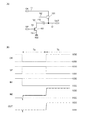
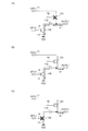
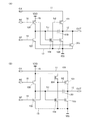
本実施の形態では、本発明の一態様に係る、基本回路、該基本回路を用いた順序回路、及び該順序回路を用いたシフトレジスタ回路について説明する。
本実施の形態では、バッファ回路を設けた基本回路、及び該基本回路を用いた順序回路について説明する。
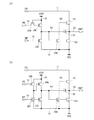
本実施の形態では、実施の形態1及び実施の形態2とは異なる順序回路について説明する。
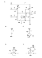
EL表示装置を例に挙げて、本発明の一態様に係る表示装置の、画素と駆動回路の断面構造について、図12を用いて説明する。図12に、画素840と駆動回路841の断面図を一例として示す。
図14に、表示装置の一形態に相当する、パネルの一例について説明する。図14に示すパネルは、基板700と、基板700上の画素部701、信号線駆動回路702、走査線駆動回路703、及び端子704とを有する。
本発明の一態様に係る半導体装置は、表示機器、パーソナルコンピュータ、記録媒体を備えた画像再生装置(代表的にはDVD:Digital Versatile Disc等の記録媒体を再生し、その画像を表示しうるディスプレイを有する装置)に用いることができる。その他に、本発明の一態様に係る半導体装置を用いることができる電子機器として、携帯電話、携帯型を含むゲーム機、携帯情報端末、電子書籍、ビデオカメラやデジタルスチルカメラなどのカメラ、ゴーグル型ディスプレイ(ヘッドマウントディスプレイ)、ナビゲーションシステム、音響再生装置(カーオーディオ、デジタルオーディオプレイヤー等)、複写機、ファクシミリ、プリンター、プリンター複合機、現金自動預け入れ払い機(ATM)、自動販売機などが挙げられる。これら電子機器の具体例を図15に示す。
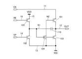
M3 トランジスタ
M7 トランジスタ
N1 ノード
N2 ノード
11 配線
12 配線
13 配線
14 配線
15 配線
16 配線
17 配線
21 配線
21[i] 配線
21[i−1] 配線
21[N] 配線
21[1] 配線
22 配線
23 配線
24 配線
31 配線
100 順序回路
100[1] 順序回路
100[3] 順序回路
101 トランジスタ
102 トランジスタ
103 トランジスタ
104 トランジスタ
105 トランジスタ
110 容量素子
201 トランジスタ
202 トランジスタ
301 容量素子
302 トランジスタ
303 トランジスタ
304 トランジスタ
305 トランジスタ
306 トランジスタ
307 トランジスタ
308 回路
308a トランジスタ
308b トランジスタ
308c トランジスタ
308d トランジスタ
308e トランジスタ
700 基板
701 画素部
702 信号線駆動回路
703 走査線駆動回路
704 端子
800 基板
802 ゲート絶縁膜
812 導電膜
813 半導体膜
814 導電膜
815 導電膜
816 導電膜
817 半導体膜
818 導電膜
819 導電膜
820 絶縁膜
821 絶縁膜
822 導電膜
823 コンタクトホール
824 絶縁膜
825 EL層
826 導電膜
830 トランジスタ
831 トランジスタ
832 発光素子
833 容量素子
840 画素
841 駆動回路
1602 ゲート電極
1603 ゲート絶縁膜
1604 半導体膜
1605 導電膜
1606 導電膜
1607 絶縁膜
1612 ゲート電極
1613 ゲート絶縁膜
1614 半導体膜
1615 導電膜
1616 導電膜
1617 絶縁膜
1618 チャネル保護膜
1622 ゲート電極
1623 ゲート絶縁膜
1624 半導体膜
1625 導電膜
1626 導電膜
1627 絶縁膜
1642 ゲート電極
1643 ゲート絶縁膜
1644 半導体膜
1645 導電膜
1646 導電膜
1647 絶縁膜
5001 筐体
5002 筐体
5003 表示部
5004 表示部
5005 マイクロホン
5006 スピーカー
5007 操作キー
5008 スタイラス
5201 筐体
5202 表示部
5203 支持台
5401 筐体
5402 表示部
5403 キーボード
5404 ポインティングデバイス
5601 筐体
5602 筐体
5603 表示部
5604 表示部
5605 接続部
5606 操作キー
5801 筐体
5802 表示部
5803 音声入力部
5804 音声出力部
5805 操作キー
5806 受光部
Claims (5)
- 第1のトランジスタと、第2のトランジスタと、容量素子と、を有し、
前記第1のトランジスタのソース又はドレインの一方は、第1の配線と電気的に接続され、
前記第1のトランジスタのソース又はドレインの他方は、第2の配線と電気的に接続され、
前記第2のトランジスタのソース又はドレインの一方は、第3の配線と電気的に接続され、
前記第2のトランジスタのゲートは、第4の配線と電気的に接続され、
前記容量素子の第1の電極は、前記第2の配線と電気的に接続され、
前記容量素子の第2の電極は、前記第2のトランジスタのソース又はドレインの他方と電気的に接続され、
前記容量素子の第2の電極は、前記第1のトランジスタのゲートと直接接続されておらず、
前記第1の配線は、第1の信号を供給することができる機能を有し、
前記第4の配線は、第2の信号を供給することができる機能を有することを特徴とする半導体装置。 - 請求項1において、
第3のトランジスタを有し、
前記第3のトランジスタのソース又はドレインの一方は、前記第1のトランジスタのソース又はドレインの一方と電気的に接続され、
前記第3のトランジスタのゲートは、前記第1のトランジスタのゲートと電気的に接続されることを特徴とする半導体装置。 - 請求項1又は請求項2において、
前記第1のトランジスタのW(Wはチャネル幅)/L(Lはチャネル長)比は、前記第2のトランジスタのW/L比よりも大きい値を有することを特徴とする半導体装置。 - 請求項1乃至請求項3のいずれか一項において、
前記第1のトランジスタのソース又はドレインの他方の電位を制御することにより、前記第1のトランジスタをオンにすることを特徴とする半導体装置。 - 請求項1乃至請求項4のいずれか一項に記載の半導体装置と、
筐体、スピーカー、表示部、操作キー又は音声入力部と、
を有する電子機器。
Priority Applications (1)
| Application Number | Priority Date | Filing Date | Title |
|---|---|---|---|
| JP2012260451A JP6099372B2 (ja) | 2011-12-05 | 2012-11-29 | 半導体装置及び電子機器 |
Applications Claiming Priority (3)
| Application Number | Priority Date | Filing Date | Title |
|---|---|---|---|
| JP2011265799 | 2011-12-05 | ||
| JP2011265799 | 2011-12-05 | ||
| JP2012260451A JP6099372B2 (ja) | 2011-12-05 | 2012-11-29 | 半導体装置及び電子機器 |
Related Child Applications (1)
| Application Number | Title | Priority Date | Filing Date |
|---|---|---|---|
| JP2017029767A Division JP2017139049A (ja) | 2011-12-05 | 2017-02-21 | 半導体装置 |
Publications (3)
| Publication Number | Publication Date |
|---|---|
| JP2013140340A JP2013140340A (ja) | 2013-07-18 |
| JP2013140340A5 JP2013140340A5 (ja) | 2016-01-21 |
| JP6099372B2 true JP6099372B2 (ja) | 2017-03-22 |
Family
ID=48523376
Family Applications (8)
| Application Number | Title | Priority Date | Filing Date |
|---|---|---|---|
| JP2012260451A Active JP6099372B2 (ja) | 2011-12-05 | 2012-11-29 | 半導体装置及び電子機器 |
| JP2017029767A Withdrawn JP2017139049A (ja) | 2011-12-05 | 2017-02-21 | 半導体装置 |
| JP2019012730A Withdrawn JP2019106230A (ja) | 2011-12-05 | 2019-01-29 | 半導体装置 |
| JP2021018144A Active JP7048779B2 (ja) | 2011-12-05 | 2021-02-08 | 半導体装置 |
| JP2022048367A Active JP7238188B2 (ja) | 2011-12-05 | 2022-03-24 | 半導体装置 |
| JP2023030780A Active JP7457178B2 (ja) | 2011-12-05 | 2023-03-01 | 半導体装置 |
| JP2024039960A Active JP7631584B2 (ja) | 2011-12-05 | 2024-03-14 | 半導体装置 |
| JP2025017403A Active JP7814573B2 (ja) | 2011-12-05 | 2025-02-05 | 半導体装置 |
Family Applications After (7)
| Application Number | Title | Priority Date | Filing Date |
|---|---|---|---|
| JP2017029767A Withdrawn JP2017139049A (ja) | 2011-12-05 | 2017-02-21 | 半導体装置 |
| JP2019012730A Withdrawn JP2019106230A (ja) | 2011-12-05 | 2019-01-29 | 半導体装置 |
| JP2021018144A Active JP7048779B2 (ja) | 2011-12-05 | 2021-02-08 | 半導体装置 |
| JP2022048367A Active JP7238188B2 (ja) | 2011-12-05 | 2022-03-24 | 半導体装置 |
| JP2023030780A Active JP7457178B2 (ja) | 2011-12-05 | 2023-03-01 | 半導体装置 |
| JP2024039960A Active JP7631584B2 (ja) | 2011-12-05 | 2024-03-14 | 半導体装置 |
| JP2025017403A Active JP7814573B2 (ja) | 2011-12-05 | 2025-02-05 | 半導体装置 |
Country Status (2)
| Country | Link |
|---|---|
| US (2) | US8872299B2 (ja) |
| JP (8) | JP6099372B2 (ja) |
Families Citing this family (9)
| Publication number | Priority date | Publication date | Assignee | Title |
|---|---|---|---|---|
| US8736315B2 (en) | 2011-09-30 | 2014-05-27 | Semiconductor Energy Laboratory Co., Ltd. | Semiconductor device |
| US9742378B2 (en) | 2012-06-29 | 2017-08-22 | Semiconductor Energy Laboratory Co., Ltd. | Pulse output circuit and semiconductor device |
| US9070546B2 (en) | 2012-09-07 | 2015-06-30 | Semiconductor Energy Laboratory Co., Ltd. | Semiconductor device |
| WO2014112299A1 (ja) * | 2013-01-21 | 2014-07-24 | シャープ株式会社 | 表示装置、および表示装置におけるデータ処理方法 |
| JP6475424B2 (ja) | 2013-06-05 | 2019-02-27 | 株式会社半導体エネルギー研究所 | 半導体装置 |
| KR102397388B1 (ko) * | 2014-07-24 | 2022-05-13 | 가부시키가이샤 한도오따이 에네루기 켄큐쇼 | 반도체 장치, 표시 모듈 및 전자 기기 |
| CN105590601B (zh) * | 2015-12-18 | 2018-06-26 | 上海中航光电子有限公司 | 驱动电路、阵列基板及显示装置 |
| CN107958656B (zh) | 2018-01-08 | 2019-07-02 | 武汉华星光电技术有限公司 | Goa电路 |
| JP2020202613A (ja) | 2019-06-06 | 2020-12-17 | 国立大学法人 東京大学 | 静電型デバイスおよび静電型デバイス製造方法 |
Family Cites Families (59)
| Publication number | Priority date | Publication date | Assignee | Title |
|---|---|---|---|---|
| US7030921B2 (en) * | 2000-02-01 | 2006-04-18 | Minolta Co., Ltd. | Solid-state image-sensing device |
| JP4785271B2 (ja) | 2001-04-27 | 2011-10-05 | 株式会社半導体エネルギー研究所 | 液晶表示装置、電子機器 |
| US6788108B2 (en) * | 2001-07-30 | 2004-09-07 | Semiconductor Energy Laboratory Co., Ltd. | Semiconductor device |
| TW564429B (en) * | 2002-08-08 | 2003-12-01 | Au Optronics Corp | Shift register circuit |
| KR100797522B1 (ko) * | 2002-09-05 | 2008-01-24 | 삼성전자주식회사 | 쉬프트 레지스터와 이를 구비하는 액정 표시 장치 |
| JP4425547B2 (ja) * | 2003-01-17 | 2010-03-03 | 株式会社半導体エネルギー研究所 | パルス出力回路、シフトレジスタ、および電子機器 |
| US7369111B2 (en) | 2003-04-29 | 2008-05-06 | Samsung Electronics Co., Ltd. | Gate driving circuit and display apparatus having the same |
| KR100965161B1 (ko) * | 2003-06-12 | 2010-06-24 | 삼성전자주식회사 | 유기전계발광 구동회로와, 이를 갖는 표시패널 및 표시장치 |
| KR101057297B1 (ko) * | 2004-08-31 | 2011-08-22 | 엘지디스플레이 주식회사 | 내장형 게이트 드라이버 및 이를 구비한 표시장치 |
| JP2006164477A (ja) * | 2004-12-10 | 2006-06-22 | Casio Comput Co Ltd | シフトレジスタ、該シフトレジスタの駆動制御方法及び該シフトレジスタを備えた表示駆動装置 |
| JP4111205B2 (ja) * | 2005-05-23 | 2008-07-02 | 日本電気株式会社 | 半導体装置、液晶ディスプレイパネル及び電子機器並びに半導体装置の設計方法及び製造方法 |
| EP1998373A3 (en) | 2005-09-29 | 2012-10-31 | Semiconductor Energy Laboratory Co, Ltd. | Semiconductor device having oxide semiconductor layer and manufacturing method thereof |
| KR101437086B1 (ko) * | 2006-01-07 | 2014-09-03 | 가부시키가이샤 한도오따이 에네루기 켄큐쇼 | 반도체장치와, 이 반도체장치를 구비한 표시장치 및 전자기기 |
| JP5164383B2 (ja) * | 2006-01-07 | 2013-03-21 | 株式会社半導体エネルギー研究所 | 半導体装置、表示装置、液晶表示装置、表示モジュール及び電子機器 |
| TWI347577B (en) * | 2006-09-01 | 2011-08-21 | Au Optronics Corp | Shift register with low stress |
| JP5116277B2 (ja) | 2006-09-29 | 2013-01-09 | 株式会社半導体エネルギー研究所 | 半導体装置、表示装置、液晶表示装置、表示モジュール及び電子機器 |
| JP5468196B2 (ja) * | 2006-09-29 | 2014-04-09 | 株式会社半導体エネルギー研究所 | 半導体装置、表示装置及び液晶表示装置 |
| JP4990034B2 (ja) * | 2006-10-03 | 2012-08-01 | 三菱電機株式会社 | シフトレジスタ回路およびそれを備える画像表示装置 |
| JP5079301B2 (ja) * | 2006-10-26 | 2012-11-21 | 三菱電機株式会社 | シフトレジスタ回路およびそれを備える画像表示装置 |
| JP5241724B2 (ja) * | 2007-09-12 | 2013-07-17 | シャープ株式会社 | シフトレジスタ |
| JP2010033690A (ja) * | 2008-06-30 | 2010-02-12 | Mitsubishi Electric Corp | シフトレジスタ回路 |
| JP5434007B2 (ja) * | 2008-08-01 | 2014-03-05 | カシオ計算機株式会社 | フリップフロップ回路、シフトレジスタ及び電子機器 |
| CN101714546B (zh) | 2008-10-03 | 2014-05-14 | 株式会社半导体能源研究所 | 显示装置及其制造方法 |
| KR101259727B1 (ko) | 2008-10-24 | 2013-04-30 | 가부시키가이샤 한도오따이 에네루기 켄큐쇼 | 반도체 장치 |
| KR101634411B1 (ko) | 2008-10-31 | 2016-06-28 | 가부시키가이샤 한도오따이 에네루기 켄큐쇼 | 구동 회로, 표시 장치 및 전자 장치 |
| JP5436049B2 (ja) * | 2009-05-29 | 2014-03-05 | 三菱電機株式会社 | シフトレジスタ回路、シフトレジスタ回路の設計方法及び半導体装置 |
| WO2011010546A1 (en) * | 2009-07-24 | 2011-01-27 | Semiconductor Energy Laboratory Co., Ltd. | Semiconductor device |
| EP2284891B1 (en) * | 2009-08-07 | 2019-07-24 | Semiconductor Energy Laboratory Co, Ltd. | Semiconductor device and manufacturing method thereof |
| KR101746198B1 (ko) | 2009-09-04 | 2017-06-12 | 가부시키가이샤 한도오따이 에네루기 켄큐쇼 | 표시장치 및 전자기기 |
| CN102012591B (zh) * | 2009-09-04 | 2012-05-30 | 北京京东方光电科技有限公司 | 移位寄存器单元及液晶显示器栅极驱动装置 |
| WO2011043451A1 (en) | 2009-10-09 | 2011-04-14 | Semiconductor Energy Laboratory Co., Ltd. | Shift register and display device |
| JP2011085680A (ja) * | 2009-10-14 | 2011-04-28 | Epson Imaging Devices Corp | 液晶表示装置、走査線駆動回路および電子機器 |
| WO2011046025A1 (en) | 2009-10-16 | 2011-04-21 | Semiconductor Energy Laboratory Co., Ltd. | Logic circuit and semiconductor device |
| KR101591613B1 (ko) | 2009-10-21 | 2016-02-03 | 가부시키가이샤 한도오따이 에네루기 켄큐쇼 | 반도체 장치 |
| CN106057819B (zh) | 2009-10-30 | 2019-03-15 | 株式会社半导体能源研究所 | 半导体装置 |
| WO2011070929A1 (en) | 2009-12-11 | 2011-06-16 | Semiconductor Energy Laboratory Co., Ltd. | Semiconductor device and electronic device |
| KR20120115318A (ko) | 2009-12-23 | 2012-10-17 | 가부시키가이샤 한도오따이 에네루기 켄큐쇼 | 반도체 장치 |
| CN105590646B (zh) | 2009-12-25 | 2019-01-08 | 株式会社半导体能源研究所 | 存储器装置、半导体器件和电子装置 |
| EP2526619B1 (en) | 2010-01-20 | 2016-03-23 | Semiconductor Energy Laboratory Co. Ltd. | Signal processing circuit and method for driving the same |
| WO2011096153A1 (en) * | 2010-02-05 | 2011-08-11 | Semiconductor Energy Laboratory Co., Ltd. | Display device |
| WO2011096286A1 (en) | 2010-02-05 | 2011-08-11 | Semiconductor Energy Laboratory Co., Ltd. | Field effect transistor and semiconductor device |
| JP5465029B2 (ja) * | 2010-02-09 | 2014-04-09 | 株式会社ジャパンディスプレイ | 表示装置および電子機器 |
| KR101774470B1 (ko) * | 2010-02-18 | 2017-09-04 | 가부시키가이샤 한도오따이 에네루기 켄큐쇼 | 표시 장치 및 전자 장치 |
| KR101772246B1 (ko) | 2010-02-23 | 2017-08-28 | 가부시키가이샤 한도오따이 에네루기 켄큐쇼 | 표시 장치, 반도체 장치, 및 그 구동 방법 |
| CN105245218B (zh) * | 2010-03-02 | 2019-01-22 | 株式会社半导体能源研究所 | 脉冲信号输出电路和移位寄存器 |
| KR101570853B1 (ko) * | 2010-03-02 | 2015-11-20 | 가부시키가이샤 한도오따이 에네루기 켄큐쇼 | 펄스 신호 출력 회로 및 시프트 레지스터 |
| KR101817926B1 (ko) | 2010-03-02 | 2018-01-12 | 가부시키가이샤 한도오따이 에네루기 켄큐쇼 | 승압 회로 및 승압 회로를 포함하는 rfid 태그 |
| JP5678730B2 (ja) * | 2010-03-30 | 2015-03-04 | ソニー株式会社 | インバータ回路および表示装置 |
| US8300039B2 (en) * | 2010-03-30 | 2012-10-30 | Sony Corporation | Inverter circuit and display |
| KR101674690B1 (ko) * | 2010-03-30 | 2016-11-09 | 가부시키가이샤 제이올레드 | 인버터 회로 및 표시 장치 |
| TWI427587B (zh) * | 2010-05-11 | 2014-02-21 | Innolux Corp | 顯示器 |
| US8664658B2 (en) | 2010-05-14 | 2014-03-04 | Semiconductor Energy Laboratory Co., Ltd. | Semiconductor device |
| JP5714973B2 (ja) | 2010-05-21 | 2015-05-07 | 株式会社半導体エネルギー研究所 | 半導体装置 |
| JP2013009285A (ja) | 2010-08-26 | 2013-01-10 | Semiconductor Energy Lab Co Ltd | 信号処理回路及びその駆動方法 |
| JP5827520B2 (ja) | 2010-09-13 | 2015-12-02 | 株式会社半導体エネルギー研究所 | 半導体記憶装置 |
| TWI543158B (zh) | 2010-10-25 | 2016-07-21 | 半導體能源研究所股份有限公司 | 半導體儲存裝置及其驅動方法 |
| TWI632551B (zh) | 2010-12-03 | 2018-08-11 | 半導體能源研究所股份有限公司 | 積體電路,其驅動方法,及半導體裝置 |
| JP5859839B2 (ja) | 2011-01-14 | 2016-02-16 | 株式会社半導体エネルギー研究所 | 記憶素子の駆動方法、及び、記憶素子 |
| US8736315B2 (en) * | 2011-09-30 | 2014-05-27 | Semiconductor Energy Laboratory Co., Ltd. | Semiconductor device |
-
2012
- 2012-11-29 JP JP2012260451A patent/JP6099372B2/ja active Active
- 2012-12-04 US US13/693,208 patent/US8872299B2/en active Active
-
2014
- 2014-10-23 US US14/521,513 patent/US9245909B2/en active Active
-
2017
- 2017-02-21 JP JP2017029767A patent/JP2017139049A/ja not_active Withdrawn
-
2019
- 2019-01-29 JP JP2019012730A patent/JP2019106230A/ja not_active Withdrawn
-
2021
- 2021-02-08 JP JP2021018144A patent/JP7048779B2/ja active Active
-
2022
- 2022-03-24 JP JP2022048367A patent/JP7238188B2/ja active Active
-
2023
- 2023-03-01 JP JP2023030780A patent/JP7457178B2/ja active Active
-
2024
- 2024-03-14 JP JP2024039960A patent/JP7631584B2/ja active Active
-
2025
- 2025-02-05 JP JP2025017403A patent/JP7814573B2/ja active Active
Also Published As
| Publication number | Publication date |
|---|---|
| JP7457178B2 (ja) | 2024-03-27 |
| US9245909B2 (en) | 2016-01-26 |
| JP7631584B2 (ja) | 2025-02-18 |
| JP2022104935A (ja) | 2022-07-12 |
| JP2023080066A (ja) | 2023-06-08 |
| JP2019106230A (ja) | 2019-06-27 |
| JP2025065292A (ja) | 2025-04-17 |
| US8872299B2 (en) | 2014-10-28 |
| US20130140617A1 (en) | 2013-06-06 |
| US20150053986A1 (en) | 2015-02-26 |
| JP7814573B2 (ja) | 2026-02-16 |
| JP7048779B2 (ja) | 2022-04-05 |
| JP2024079721A (ja) | 2024-06-11 |
| JP7238188B2 (ja) | 2023-03-13 |
| JP2017139049A (ja) | 2017-08-10 |
| JP2013140340A (ja) | 2013-07-18 |
| JP2021099894A (ja) | 2021-07-01 |
Similar Documents
| Publication | Publication Date | Title |
|---|---|---|
| JP7453439B2 (ja) | 半導体装置 | |
| JP7457178B2 (ja) | 半導体装置 | |
| JP2026074137A (ja) | 半導体装置 |
Legal Events
| Date | Code | Title | Description |
|---|---|---|---|
| A521 | Request for written amendment filed |
Free format text: JAPANESE INTERMEDIATE CODE: A523 Effective date: 20151125 |
|
| A621 | Written request for application examination |
Free format text: JAPANESE INTERMEDIATE CODE: A621 Effective date: 20151125 |
|
| A977 | Report on retrieval |
Free format text: JAPANESE INTERMEDIATE CODE: A971007 Effective date: 20160914 |
|
| A131 | Notification of reasons for refusal |
Free format text: JAPANESE INTERMEDIATE CODE: A131 Effective date: 20160920 |
|
| A521 | Request for written amendment filed |
Free format text: JAPANESE INTERMEDIATE CODE: A523 Effective date: 20161012 |
|
| TRDD | Decision of grant or rejection written | ||
| A01 | Written decision to grant a patent or to grant a registration (utility model) |
Free format text: JAPANESE INTERMEDIATE CODE: A01 Effective date: 20170214 |
|
| A61 | First payment of annual fees (during grant procedure) |
Free format text: JAPANESE INTERMEDIATE CODE: A61 Effective date: 20170221 |
|
| R150 | Certificate of patent or registration of utility model |
Ref document number: 6099372 Country of ref document: JP Free format text: JAPANESE INTERMEDIATE CODE: R150 |
|
| R250 | Receipt of annual fees |
Free format text: JAPANESE INTERMEDIATE CODE: R250 |
|
| R250 | Receipt of annual fees |
Free format text: JAPANESE INTERMEDIATE CODE: R250 |
|
| R250 | Receipt of annual fees |
Free format text: JAPANESE INTERMEDIATE CODE: R250 |
|
| R250 | Receipt of annual fees |
Free format text: JAPANESE INTERMEDIATE CODE: R250 |
|
| R250 | Receipt of annual fees |
Free format text: JAPANESE INTERMEDIATE CODE: R250 |
|
| R250 | Receipt of annual fees |
Free format text: JAPANESE INTERMEDIATE CODE: R250 |
|
| R250 | Receipt of annual fees |
Free format text: JAPANESE INTERMEDIATE CODE: R250 |