JP6095258B2 - Solid-state imaging device and imaging system using solid-state imaging device - Google Patents
Solid-state imaging device and imaging system using solid-state imaging device Download PDFInfo
- Publication number
- JP6095258B2 JP6095258B2 JP2011119258A JP2011119258A JP6095258B2 JP 6095258 B2 JP6095258 B2 JP 6095258B2 JP 2011119258 A JP2011119258 A JP 2011119258A JP 2011119258 A JP2011119258 A JP 2011119258A JP 6095258 B2 JP6095258 B2 JP 6095258B2
- Authority
- JP
- Japan
- Prior art keywords
- gate electrode
- solid
- imaging device
- state imaging
- light shielding
- Prior art date
- Legal status (The legal status is an assumption and is not a legal conclusion. Google has not performed a legal analysis and makes no representation as to the accuracy of the status listed.)
- Expired - Fee Related
Links
- 238000003384 imaging method Methods 0.000 title claims description 65
- 239000004065 semiconductor Substances 0.000 claims description 45
- 239000000758 substrate Substances 0.000 claims description 32
- 238000006243 chemical reaction Methods 0.000 claims description 31
- 238000009792 diffusion process Methods 0.000 claims description 8
- 238000000034 method Methods 0.000 claims description 4
- 238000002955 isolation Methods 0.000 description 7
- 229910052751 metal Inorganic materials 0.000 description 5
- 239000002184 metal Substances 0.000 description 5
- 238000009825 accumulation Methods 0.000 description 4
- 238000010586 diagram Methods 0.000 description 4
- 239000010410 layer Substances 0.000 description 4
- 230000003321 amplification Effects 0.000 description 3
- 238000003199 nucleic acid amplification method Methods 0.000 description 3
- VYPSYNLAJGMNEJ-UHFFFAOYSA-N Silicium dioxide Chemical compound O=[Si]=O VYPSYNLAJGMNEJ-UHFFFAOYSA-N 0.000 description 2
- 239000004020 conductor Substances 0.000 description 2
- 238000007599 discharging Methods 0.000 description 2
- 239000000463 material Substances 0.000 description 2
- 229910052814 silicon oxide Inorganic materials 0.000 description 2
- 229910052782 aluminium Inorganic materials 0.000 description 1
- XAGFODPZIPBFFR-UHFFFAOYSA-N aluminium Chemical compound [Al] XAGFODPZIPBFFR-UHFFFAOYSA-N 0.000 description 1
- 230000015572 biosynthetic process Effects 0.000 description 1
- 238000005530 etching Methods 0.000 description 1
- 239000011229 interlayer Substances 0.000 description 1
- 238000004519 manufacturing process Methods 0.000 description 1
- 239000011159 matrix material Substances 0.000 description 1
- 238000002156 mixing Methods 0.000 description 1
- 230000003647 oxidation Effects 0.000 description 1
- 238000007254 oxidation reaction Methods 0.000 description 1
- 229910021420 polycrystalline silicon Inorganic materials 0.000 description 1
- 229920005591 polysilicon Polymers 0.000 description 1
- 229910052710 silicon Inorganic materials 0.000 description 1
- 239000010703 silicon Substances 0.000 description 1
- WFKWXMTUELFFGS-UHFFFAOYSA-N tungsten Chemical compound [W] WFKWXMTUELFFGS-UHFFFAOYSA-N 0.000 description 1
- 229910052721 tungsten Inorganic materials 0.000 description 1
- 239000010937 tungsten Substances 0.000 description 1
Images


Classifications
-
- H—ELECTRICITY
- H01—ELECTRIC ELEMENTS
- H01L—SEMICONDUCTOR DEVICES NOT COVERED BY CLASS H10
- H01L27/00—Devices consisting of a plurality of semiconductor or other solid-state components formed in or on a common substrate
- H01L27/14—Devices consisting of a plurality of semiconductor or other solid-state components formed in or on a common substrate including semiconductor components sensitive to infrared radiation, light, electromagnetic radiation of shorter wavelength or corpuscular radiation and specially adapted either for the conversion of the energy of such radiation into electrical energy or for the control of electrical energy by such radiation
- H01L27/144—Devices controlled by radiation
- H01L27/146—Imager structures
- H01L27/14601—Structural or functional details thereof
- H01L27/14603—Special geometry or disposition of pixel-elements, address-lines or gate-electrodes
-
- H—ELECTRICITY
- H01—ELECTRIC ELEMENTS
- H01L—SEMICONDUCTOR DEVICES NOT COVERED BY CLASS H10
- H01L27/00—Devices consisting of a plurality of semiconductor or other solid-state components formed in or on a common substrate
- H01L27/14—Devices consisting of a plurality of semiconductor or other solid-state components formed in or on a common substrate including semiconductor components sensitive to infrared radiation, light, electromagnetic radiation of shorter wavelength or corpuscular radiation and specially adapted either for the conversion of the energy of such radiation into electrical energy or for the control of electrical energy by such radiation
- H01L27/144—Devices controlled by radiation
- H01L27/146—Imager structures
- H01L27/14601—Structural or functional details thereof
- H01L27/1462—Coatings
- H01L27/14623—Optical shielding
-
- H—ELECTRICITY
- H01—ELECTRIC ELEMENTS
- H01L—SEMICONDUCTOR DEVICES NOT COVERED BY CLASS H10
- H01L27/00—Devices consisting of a plurality of semiconductor or other solid-state components formed in or on a common substrate
- H01L27/14—Devices consisting of a plurality of semiconductor or other solid-state components formed in or on a common substrate including semiconductor components sensitive to infrared radiation, light, electromagnetic radiation of shorter wavelength or corpuscular radiation and specially adapted either for the conversion of the energy of such radiation into electrical energy or for the control of electrical energy by such radiation
- H01L27/144—Devices controlled by radiation
- H01L27/146—Imager structures
- H01L27/14601—Structural or functional details thereof
- H01L27/14609—Pixel-elements with integrated switching, control, storage or amplification elements
- H01L27/14612—Pixel-elements with integrated switching, control, storage or amplification elements involving a transistor
- H01L27/14614—Pixel-elements with integrated switching, control, storage or amplification elements involving a transistor having a special gate structure
-
- H—ELECTRICITY
- H01—ELECTRIC ELEMENTS
- H01L—SEMICONDUCTOR DEVICES NOT COVERED BY CLASS H10
- H01L27/00—Devices consisting of a plurality of semiconductor or other solid-state components formed in or on a common substrate
- H01L27/14—Devices consisting of a plurality of semiconductor or other solid-state components formed in or on a common substrate including semiconductor components sensitive to infrared radiation, light, electromagnetic radiation of shorter wavelength or corpuscular radiation and specially adapted either for the conversion of the energy of such radiation into electrical energy or for the control of electrical energy by such radiation
- H01L27/144—Devices controlled by radiation
- H01L27/146—Imager structures
- H01L27/14601—Structural or functional details thereof
- H01L27/14609—Pixel-elements with integrated switching, control, storage or amplification elements
- H01L27/14612—Pixel-elements with integrated switching, control, storage or amplification elements involving a transistor
-
- H—ELECTRICITY
- H01—ELECTRIC ELEMENTS
- H01L—SEMICONDUCTOR DEVICES NOT COVERED BY CLASS H10
- H01L27/00—Devices consisting of a plurality of semiconductor or other solid-state components formed in or on a common substrate
- H01L27/14—Devices consisting of a plurality of semiconductor or other solid-state components formed in or on a common substrate including semiconductor components sensitive to infrared radiation, light, electromagnetic radiation of shorter wavelength or corpuscular radiation and specially adapted either for the conversion of the energy of such radiation into electrical energy or for the control of electrical energy by such radiation
- H01L27/144—Devices controlled by radiation
- H01L27/146—Imager structures
- H01L27/14643—Photodiode arrays; MOS imagers
-
- H—ELECTRICITY
- H04—ELECTRIC COMMUNICATION TECHNIQUE
- H04N—PICTORIAL COMMUNICATION, e.g. TELEVISION
- H04N25/00—Circuitry of solid-state image sensors [SSIS]; Control thereof
- H04N25/70—SSIS architectures; Circuits associated therewith
- H04N25/76—Addressed sensors, e.g. MOS or CMOS sensors
Landscapes
- Engineering & Computer Science (AREA)
- Physics & Mathematics (AREA)
- Power Engineering (AREA)
- Electromagnetism (AREA)
- Condensed Matter Physics & Semiconductors (AREA)
- General Physics & Mathematics (AREA)
- Computer Hardware Design (AREA)
- Microelectronics & Electronic Packaging (AREA)
- Multimedia (AREA)
- Signal Processing (AREA)
- Solid State Image Pick-Up Elements (AREA)
- Transforming Light Signals Into Electric Signals (AREA)
Description
本発明は固体撮像装置、及び固体撮像装置を用いた撮像システムに関する。特に、画素に電荷保持部を有する固体撮像装置の遮光部に関するものである。 The present invention relates to a solid-state imaging device and an imaging system using the solid-state imaging device. In particular, the present invention relates to a light shielding unit of a solid-state imaging device having a charge holding unit in a pixel.
CMOSイメージセンサに代表されるアクティブピクセル型の固体撮像装置において、グローバル電子シャッター機能を有する固体撮像装置が提案されている。
グローバル電子シャッター機能とは、行列状に配された複数の画素の光電荷蓄積の開始時刻と終了時刻とを全画素で同時に行う機能である。グローバル電子シャッター機能を有する固体撮像装置は、画素に光電変換部と光電変換された電荷を一定時間保持しておく電荷保持部とを有する。グローバル電子シャッター機能を有する固体撮像装置の電荷保持部では、光電荷の蓄積終了後から読み出しまでの期間に電荷を保持する。この時、光電変換部以外で発生した電荷が電荷保持部に混入するとノイズ信号となり画質が劣化する可能性がある。特許文献1には、画素に光電変換部と電荷保持部とを有し、電荷保持部上に遮光部を設けた構成が開示されている。
In an active pixel type solid-state imaging device represented by a CMOS image sensor, a solid-state imaging device having a global electronic shutter function has been proposed.
The global electronic shutter function is a function that simultaneously performs the start time and the end time of photocharge accumulation of a plurality of pixels arranged in a matrix in all pixels. A solid-state imaging device having a global electronic shutter function includes a photoelectric conversion unit and a charge holding unit that holds photoelectrically converted charges for a certain period of time. In the charge holding unit of the solid-state imaging device having the global electronic shutter function, the charge is held during a period from the end of the accumulation of photocharges to the readout. At this time, if charges generated in other than the photoelectric conversion unit are mixed in the charge holding unit, a noise signal may be generated and the image quality may be deteriorated.
特許文献1に記載の構成において、遮光部は配線層を有する層間絶縁膜の上に配されており、斜め光が遮光部の開口から電荷保持部へと入射しやすい。また、素子への電圧の供給などのためコンタクトを設ける場合には、コンタクトのプラグのために遮光部に開口を設ける必要があり、より斜め光が容易に電荷保持部に入射してしまう。このような斜め光によって生じた電荷が電荷保持部で保持している画像形成用の電荷に混入してしまうと、得られる画像の劣化をもたらしてしまう。
そこで、本発明においては、遮光性能を向上させた電荷保持部を有する固体撮像装置、及びそれを用いた撮像システムを提供することを目的とする。
In the configuration described in
Accordingly, an object of the present invention is to provide a solid-state imaging device having a charge holding unit with improved light shielding performance, and an imaging system using the same.
本発明の固体撮像装置は、半導体基板と、前記半導体基板に配された光電変換部と、前記半導体基板に配され、前記光電変換部で生じた電荷を保持する電荷保持部と、前記半導体基板に配され、前記電荷保持部で保持された電荷が転送されるフローティングディフュージョン部と、前記半導体基板上に配され、前記光電変換部と前記電荷保持部との間に配された第1のゲート電極と、前記半導体基板上に配され、前記電荷保持部と前記フローティングディフュージョン部との間に配された第2のゲート電極と、を有する固体撮像装置において、前記電荷保持部の上と、少なくとも前記第1のゲート電極あるいは前記第2のゲート電極の上とに配された第1の部分と、前記第1のゲート電極と前記第2のゲート電極との間であって、前記半導体基板の表面側に前記第1の部分から延在した第2の部分と、によって構成される遮光部を有する。 The solid-state imaging device of the present invention includes a semiconductor substrate, a photoelectric conversion unit disposed on the semiconductor substrate, a charge holding unit disposed on the semiconductor substrate and holding charges generated in the photoelectric conversion unit, and the semiconductor substrate A floating diffusion portion to which the charge held in the charge holding portion is transferred, and a first gate arranged on the semiconductor substrate and arranged between the photoelectric conversion portion and the charge holding portion In a solid-state imaging device, comprising: an electrode; and a second gate electrode disposed on the semiconductor substrate and disposed between the charge retaining portion and the floating diffusion portion, at least on the charge retaining portion, A first portion disposed on the first gate electrode or the second gate electrode, and between the first gate electrode and the second gate electrode, the semiconductor Has a second portion extending from said first portion on the surface side of the plate, the light shielding portion formed by.
本発明によれば、遮光性能を向上させた電荷保持部を有する固体撮像装置、及びそれを用いた撮像システムを提供することが可能となる。 ADVANTAGE OF THE INVENTION According to this invention, it becomes possible to provide the solid-state imaging device which has the electric charge holding part which improved the light-shielding performance, and an imaging system using the same.
本発明の固体撮像装置は、半導体基板に配された光電変換部と、電荷保持部と、フローティングディフュージョン部とを有する。そして、半導体基板上の光電変換部と電荷保持部との間には第1のゲート電極が配され、半導体基板上の電荷保持部とフローティングディフュージョン部との間には第2のゲート電極が配される。そして、本発明の固体撮像装置は、電荷保持部の上と、少なくとも第1のゲート電極あるいは第2のゲート電極の上に配された第1の部分を有する遮光部を有する。ここで、遮光部は、第1のゲート電極と第2のゲート電極との間に配され、半導体基板の表面側に第1の部分から延在した第2の部分と、を有する。このような構成によって、斜め光の電荷保持部への入射を抑制し、遮光性能を向上させることが可能となる。 The solid-state imaging device of the present invention includes a photoelectric conversion unit, a charge holding unit, and a floating diffusion unit arranged on a semiconductor substrate. A first gate electrode is disposed between the photoelectric conversion unit and the charge holding unit on the semiconductor substrate, and a second gate electrode is disposed between the charge holding unit and the floating diffusion unit on the semiconductor substrate. Is done. The solid-state imaging device according to the present invention includes a light-shielding portion having a first portion disposed on the charge holding portion and at least the first gate electrode or the second gate electrode. Here, the light shielding portion includes a second portion that is disposed between the first gate electrode and the second gate electrode and extends from the first portion on the surface side of the semiconductor substrate. With such a configuration, it is possible to suppress the incidence of oblique light to the charge holding unit and improve the light shielding performance.
以下、ある部材と別の部材との接続のための導電体からなるプラグをコンタクトプラグと称する。また、半導体基板の表面から半導体基板の内部へ向かう方向を下方向とし、その反対を上の方向とする。 Hereinafter, a plug made of a conductor for connecting one member to another member is referred to as a contact plug. The direction from the surface of the semiconductor substrate toward the inside of the semiconductor substrate is the downward direction, and the opposite is the upward direction.
(実施例1)
本実施例の固体撮像装置について、図1乃至3を用いて説明する。
Example 1
The solid-state imaging device of this embodiment will be described with reference to FIGS.
まず、図1は本実施例の固体撮像装置の4画素分の回路図を示している。図1において、画素100は2行2列で配列されている。画素100は、光電変換部101、電荷保持部102、第1の転送用トランジスタ104、第2の転送用トランジスタ105、増幅用トランジスタ106、選択用トランジスタ107、リセット用トランジスタ108と、を含む。更に、画素100は、不要電荷排出用のオーバーフロードレイン(以下OFD)のための第3の転送用トランジスタ109を含む。画素100において、103は浮遊拡散部(フローティングディフュージョン部、以下FD部)を含むノードである。電源線110及び電源線111は所定の電圧を供給する配線である。電源線110はOFD用のトランジスタ109の主電極領域と接続している。電源線111は、リセット用トランジスタ及び選択用トランジスタの主電極領域と接続している。RES、TX1、TX2、SEL、TX3は各トランジスタのゲート電極にパルスを供給する制御線であり、垂直走査回路(不図示)からパルスが供給される。RESはリセット用トランジスタ108、TX1は第1の転送用トランジスタ104、TX2は第2の転送用トランジスタ105のゲート電極にパルスを供給する制御線である。SELは選択用トランジスタ107、TX3は第3の転送用トランジスタ109のゲート電極にパルスを供給する制御線である。OUTは信号線である。図1に示されているnやmは自然数であり、ある行nとその隣の行n+1、ある列mとその隣の列m+1とを示している。信号線OUTから出力された信号は読み出し回路(不図示)に保持され、増幅や加算等の処理がなされ、固体撮像装置の外部へ信号が出力される。この時、信号の加算等の処理や外部への信号出力を制御する制御信号が水平走査回路(不図示)から供給されうる。また、信号線OUTには増幅用トランジスタとソースフォロア回路を構成する定電流源が設けられる。図1において、画素100とは、1つの光電変換部101を含む構成であり、光電変換装置の構成における最小の繰り返し単位である。
First, FIG. 1 shows a circuit diagram for four pixels of the solid-state imaging device of the present embodiment. In FIG. 1, the
図1の画素100における、グローバルシャッターの動作は次のようになる。ある蓄積期間が経過した後に、光電変換部101にて生じた電荷は、第1の転送用トランジスタ104を介して、電荷保持部102へと転送される。電荷保持部102にてある蓄積期間の信号電荷を保持している間、光電変換部101では再び信号電荷の蓄積が始まる。電荷保持部102の信号電荷は第2の転送用トランジスタ105を介してFD部を含むノード103へと転送され、増幅用トランジスタ106から信号として出力される。また、電荷保持部102にて信号電荷を保持している間に光電変換部101にて生じた電荷が電荷保持部102へ混入しないように、第3の転送用トランジスタ109によって光電変換部101の電荷を排出させる場合もある。リセット用トランジスタ108は、電荷保持部102から信号電荷が転送される前にFD部を含むノード103を所定の電位に設定する(リセット動作)。この時のFD部を含むノード103の電位をノイズ信号として増幅用トランジスタ106を介して信号線OUTへ出力する。このノイズ信号と後に出力される信号電荷に基づく信号との差分をとることで、ノイズ信号を除去することが可能となる。
The operation of the global shutter in the
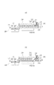
図2(a)は図1の回路図に対応した固体撮像装置の平面模式図であり、図2(b)は図2(a)のAB線における固体撮像装置の断面模式図である。図2(a)および図2(b)において、ゲート電極よりも上に配される配線層、絶縁膜などの一部の構成について省略している。 2A is a schematic plan view of the solid-state imaging device corresponding to the circuit diagram of FIG. 1, and FIG. 2B is a schematic cross-sectional view of the solid-state imaging device taken along line AB of FIG. In FIG. 2A and FIG. 2B, some configurations such as a wiring layer and an insulating film disposed above the gate electrode are omitted.
図2(a)において、画素200は、図1の画素100に対応し、2行2列に配されている。ここでは、画素200の領域を仮想的に矩形に区切っている。画素200の構成について、4つの画素のうちの1つに着目して説明する。画素200には、光電変換部201と、電荷保持部202とが隣接して配されている。光電変換部201と、電荷保持部202との間には、電荷を転送するための第1の転送用トランジスタのゲート電極204が配される。また、本実施例では、平面的に見て、ゲート電極204は電荷保持部202の全面を覆って延在している。このゲート電極204が電荷保持部202の上まで配されていることで、電荷保持部202への光の入射を低減させることが可能となる。また、電荷保持部202の上に配されているゲート電極204に供給される電圧を制御することによって、電荷保持部202の暗電流を低減することが可能である。なお、第1の転送用トランジスタの主電極領域は、光電変換部201と、電荷保持部202とを含む。さらに、画素200には、電荷保持部202から電荷を転送する第2の転送用トランジスタのゲート電極205と、FD部203と、第3の転送用トランジスタのゲート電極209とが配置されている。ゲート電極209の隣には主電極領域207が配される。主電極領域207は、光電変換部で生じた電荷のうち不要な電荷を排出する領域である。ここでゲート電極204を第1のゲート電極とし、ゲート電極205を第2のゲート電極とする。
In FIG. 2A, the
図2(a)において、コンタクトプラグ206はFD部203と増幅用トランジスタのゲート電極との接続、およびFD部203とリセット用トランジスタの主電極領域との接続のために、FD部203に配置されている。コンタクトプラグ208は、主電極領域207と電源線との接続のために、主電極領域207に配置されている。コンタクトプラグ213は、第2のゲート電極205と制御線との接続のために、第2のゲート電極205に配置されている。ここで、図1の画素100に示される画素が含む他の構成については、図2の領域211に配置されているものとする。また、以下の実施例において、信号電荷は電子であり、図1の画素100の複数のトランジスタがN型のMOSトランジスタであるとする。
In FIG. 2A, the
ここで、光電変換部202は少なくとも、電荷蓄積部として機能するN型の半導体領域を含む。電荷保持部は電荷が蓄積可能なN型の半導体領域を有する。FD部はN型の半導体領域を有し、第3の転送用トランジスタの主電極領域206はN型の半導体領域を有する。また、各素子が配置された活性領域の周囲には、素子分離領域210が配置される。素子分離領域210にはSTI(Shallow Trench Isolation)、LOCOS(Local Oxidation of Silicon)、PN接合分離などを用いた分離構造が配されている。
Here, the
図2(a)において、複数の画素200に渡って遮光部212が配されている。遮光部212は、電荷保持部202と、第2のゲート電極205の少なくとも一部の上に配されている。本実施例において遮光部212は、電荷保持部202の上と、第1のゲート電極204の上と、第2のゲート電極205の上と、素子分離領域210の一部の上に配されている。また、図2(a)に示すように、遮光部212が光電変換部の第1のゲート電極204側の一部に延在していてもよい。遮光部212は、複数のコンタクトプラグのために複数の開口214を有し、FD部203の一部と第2のゲート電極205の一部の上には配されていない。遮光部212は、光電変換部201および他のコンタクトプラグが配される領域を除いて、画素の他の構成の上に配置されていてもよい。ここで、ゲート電極204、205の材料としてはポリシリコンなど、遮光部の材料としてはタングステン、アルミニウムなどが挙げられる。
In FIG. 2A, the
図2(b)は、図2(a)のAB線における固体撮像装置の断面模式図である。図2(b)において、表面221を有するP型の半導体基板220に、図2(a)の光電変換部201を構成するN型半導体領域222と、半導体基板220の表面221側に配置されるP型半導体領域223とが配されている。また、半導体基板220に、図2(a)の電荷蓄積部202を構成するN型半導体領域224が配される。そして、半導体基板220上には、第1のゲート電極204と、第2のゲート電極205とが配されている。第2のゲート電極205の上に、第2のゲート電極205と接続するコンタクトプラグ206とが配されている。
FIG. 2B is a schematic cross-sectional view of the solid-state imaging device taken along the line AB in FIG. 2B, a P-
図2(b)において、図2(a)の遮光部212は、第1のゲート電極204および第2のゲート電極205を覆う第1の部分225に加えて、第1のゲート電極204と第2のゲート電極205との間の第2の部分226とを有する。第1の部分225および第2の部分226は、第1の部分225の底面227よりも第2の部分226の底面228は半導体基板の表面221側に位置するように構成されている。このような構成によって、コンタクトプラグ206のための遮光部212の開口214から入射する光、あるいは入射した光に伴う電荷が電荷保持部202や光電変換部201に混入することを低減することが可能となる。
In FIG. 2B, the
ここで、より詳細に第1の部分225と第2の部分226の配置を説明する。第1の部分225は第1のゲート電極204と第2のゲート電極205の上を覆い、第1のゲート電極204と第2のゲート電極205との間にも延在している。第2の部分226は、半導体基板220の表面221の上方から表面221を見た際に、各構成の形状を表面221に投影してみると、第1のゲート電極204と第2のゲート電極205との間に配される。そして、半導体基板220の表面221に対して垂直にとった断面から見ると、第2の部分226は、その底面228が半導体基板の表面221に対して第1のゲート電極204と第2のゲート電極205の底面229と同じ距離となる位置に配置されている。ここで、第2の部分226は、少なくとも、第2の部分226の底面228が第1の部分225の底面227よりも半導体基板の表面221側に位置するように配されていればよい。
ここでは、第1の部分225と第2の部分226とは一体である。よって、遮光部は、第1のゲート電極204から第2のゲート電極205へと、その間の領域を覆いつつ延在し、その間において半導体基板220の表面側に延在しているともいえる。
Here, the arrangement of the
Here, the
また、図2(b)において遮光部212は、FD部203に配されるコンタクトプラグ206(不図示)と同一高さに配され、また、遮光部212は金属で形成される配線層(不図示)の下に配されている。遮光部212を配線層よりも半導体基板の表面221側に配することで、より遮光性能を向上させることが可能となる。
In FIG. 2B, the
図2(b)の第2の部分226は、以下のように形成可能である。第1のゲート電極204と第2のゲート電極205とが形成された後、例えば酸化シリコンからなる絶縁膜を、第1のゲート電極204および第2のゲート電極205を覆い、それらの形状を踏襲するように形成する。ここで、絶縁膜は、第1のゲート電極204および第2のゲート電極205の形状を踏襲するため、その表面に凹部を有する。その後、絶縁膜上に遮光部となる金属膜を形成することで、絶縁膜の凹部に金属膜が形成される。そして、金属膜の残したい部分以外をエッチング等によって除去することで、遮光部212が形成される。
The
次に、図3を用いて、本実施例の構成について更に説明する。図3(a)は図2(b)に示した本実施例の固体撮像装置の断面模式図であり、図3(b)は比較のための固体撮像装置の断面模式図である。図3(a)と図3(b)との違いは、図3(b)は第2の部分226を有さない点である。
Next, the configuration of the present embodiment will be further described with reference to FIG. 3A is a schematic cross-sectional view of the solid-state imaging device of the present embodiment shown in FIG. 2B, and FIG. 3B is a schematic cross-sectional view of the solid-state imaging device for comparison. The difference between FIG. 3A and FIG. 3B is that FIG. 3B does not have the
図3(a)及び図3(b)において、遮光部212の開口214から同様に斜め光が入射した場合を示している。図3(b)の構成においては、光302は電荷蓄積部202などの素子に容易に入射してしまうことが分かる。また、光302が素子には入射しなかったとしても、半導体基板220に入射することで電荷が発生し電荷保持部202や光電変換部201に混入してしまう。このような電荷が電荷保持部202や光電変換部201に混入すると、画像信号にノイズが生じてしまう。一方、図3(a)においては、第2の部分226によって、光301の半導体基板301へ入射を低減することが可能となる。
3A and 3B show a case where oblique light is incident from the
また、本実施例において遮光部212は、電荷保持部202の上と、第1のゲート電極204の上と、第2のゲート電極205の上と、を覆って配置されている。詳細には、それらのコンタクトプラグを除く全面を覆って配置されている。しかし、遮光部は少なくとも第1のゲート電極204あるいは第2のゲート電極205の電荷保持部202側の一部上に配されていればよい。遮光部212は電荷保持部202のみに配置しようとすると、電荷保持部202の第1のゲート電極側の端あるいは第2のゲート電極205側の端に遮光部が覆っていない領域が生じてしまうため、ゲート電極の一部上にも配置することが好ましい。しかし、このような場合においても、図3(b)と同様に光の混入が生じる可能性があるため、図3(a)のように第2の部分226を設けることが望まれている。
In the present embodiment, the
以上、本実施例の固体撮像装置によれば、斜め光の電荷保持部への入射を抑制し、遮光性能を向上させることが可能となる。なお、本実施例においては第1のゲート電極と制御線との接続のためのコンタクトプラグはここでは省略しているが同様に遮光部212に開口214を設けてコンタクトプラグを配することが可能である。また、第1のゲート電極を隣接画素の領域に延在させコンタクトプラグを配置する場所を隣接画素の領域に配してもよい。
As described above, according to the solid-state imaging device of the present embodiment, it is possible to suppress the incidence of oblique light to the charge holding unit and improve the light shielding performance. In this embodiment, a contact plug for connecting the first gate electrode and the control line is omitted here, but it is also possible to dispose a contact plug by providing an
(実施例2)
本実施例の固体撮像装置について、図4を用いて説明する。図4(a)は固体撮像装置の平面模式図であり、図4(b)は図4(a)のCD線における固体撮像装置の断面模式図である。図4(a)および図4(b)は、図2(a)および図2(b)に対応しており、それらと同一の構成については、同じ符号を付し、説明を省略する。
(Example 2)
The solid-state imaging device of the present embodiment will be described with reference to FIG. 4A is a schematic plan view of the solid-state imaging device, and FIG. 4B is a schematic cross-sectional view of the solid-state imaging device taken along the CD line in FIG. 4 (a) and 4 (b) correspond to FIG. 2 (a) and FIG. 2 (b), and the same components are denoted by the same reference numerals and description thereof is omitted.
図4(a)において、実施例1との相違点はコンタクトプラグ401を有する点である。コンタクトプラグ401は遮光部212と第1のゲート電極204とを電気的に接続する。このような構成によって、コンタクトプラグのための遮光部の開口を設ける必要がないため、より遮光性能を高めることが可能となる。また、このような構成によって、遮光部212が第1のゲート電極204へ電圧を供給する制御線を兼ねることが可能となり、配線の数を削減することが可能となる。
In FIG. 4A, the difference from the first embodiment is that a
コンタクトプラグ401は、図4(b)に示すように、第1のゲート電極204と遮光部212の第1の部分225との間に配置されている。第1のゲート電極204と第1の部分225との間に、例えば酸化シリコンからなる絶縁膜が配されている。この絶縁膜にコンタクトホールを形成し、導電体を埋め込むことによってコンタクトプラグ401が形成される。あるいは、絶縁膜にコンタクトホールを形成した後、遮光部212となる金属膜を形成することで、遮光部212と同時にコンタクトプラグ401を形成することも可能である。この工程は一般の半導体製造技術によって形成可能であるため、詳細な説明は省略する。
As shown in FIG. 4B, the
また、図4(b)に示すように、遮光部212は第2の部分226を有することで遮光性能を向上させることが可能となる。なお、図4(b)のN型半導体領域402は図4(a)におけるFD領域203を構成する。
Further, as shown in FIG. 4B, the
以上、本実施例の固体撮像装置によれば、斜め光の電荷保持部への入射を抑制し、遮光性能を向上させることが可能となる。また、遮光部と第1のゲート電極とを接続することで、第1のゲート電極のコンタクトプラグのための遮光部の開口を削減することが可能となり、遮光性能を向上させることが可能となる。 As described above, according to the solid-state imaging device of the present embodiment, it is possible to suppress the incidence of oblique light to the charge holding unit and improve the light shielding performance. Further, by connecting the light shielding portion and the first gate electrode, it is possible to reduce the opening of the light shielding portion for the contact plug of the first gate electrode, and to improve the light shielding performance. .
(実施例3)
本実施例の固体撮像装置について、図5を用いて説明する。図5(a)は固体撮像装置の平面模式図であり、図5(b)は図5(a)のEF線における固体撮像装置の断面模式図である。図5(a)および図5(b)は、図2(a)および図2(b)、図4(a)および図4(b)に対応しており、それらと同一の構成については、同じ符号を付し、説明を省略する。
(Example 3)
The solid-state imaging device of the present embodiment will be described with reference to FIG. FIG. 5A is a schematic plan view of the solid-state imaging device, and FIG. 5B is a schematic cross-sectional view of the solid-state imaging device taken along the line EF in FIG. 5 (a) and FIG. 5 (b) correspond to FIG. 2 (a) and FIG. 2 (b), FIG. 4 (a) and FIG. 4 (b). The same reference numerals are given and description thereof is omitted.
図5(a)において、実施例2との相違点は図4(a)におけるコンタクトプラグ401ではなく、コンタクトプラグ501を有する点である。コンタクトプラグ501は遮光部212と第2のゲート電極205とを電気的に接続する。このような構成によって、コンタクトプラグのための遮光部の開口を設ける必要がないため、より遮光性能を高めることが可能となる。また、このような構成によって、遮光部212が第2のゲート電極204へ電圧を供給する制御線を兼ねることが可能となり、配線の数を削減することが可能となる。
5A, the difference from the second embodiment is that a
図5(b)に示すように、コンタクトプラグ501は、実施例2のコンタクトプラグ401と同様に、第2のゲート電極205と遮光部212の第1の部分225との間の絶縁膜中に配置されている。この構成は実施例2のコンタクトプラグ401と同様であるので詳細な説明は省略する。
As shown in FIG. 5B, the
また、図5(b)においても、遮光部212は第2の部分226を有することで遮光性能を向上させることが可能である。よって、本実施例の固体撮像装置によれば、斜め光の電荷保持部への入射を抑制し、遮光性能を向上させることが可能となる。また、遮光部と第2のゲート電極とを接続することで、コンタクトプラグのための遮光部の開口を削減することが可能となり、遮光性能を向上させることが可能となる。
In FIG. 5B as well, the
(実施例4)
本実施例の固体撮像装置について、図6を用いて説明する。図6(a)は固体撮像装置の平面模式図であり、図6(b)は図6(a)のGH線における固体撮像装置の断面模式図であり、図6(c)は図6(a)のIJ線における固体撮像装置の断面模式図である。図6(a)は図2(a)と対応しており、図6(b)および図6(c)は図2(b)に対応している。図6(a)〜(c)において、図2(a)および図2(b)と同一の構成については、同じ符号を付し、説明を省略する。
Example 4
The solid-state imaging device of the present embodiment will be described with reference to FIG. 6A is a schematic plan view of the solid-state imaging device, FIG. 6B is a schematic cross-sectional view of the solid-state imaging device taken along the line GH in FIG. 6A, and FIG. It is a cross-sectional schematic diagram of the solid-state imaging device in the IJ line of a). 6 (a) corresponds to FIG. 2 (a), and FIGS. 6 (b) and 6 (c) correspond to FIG. 2 (b). 6 (a) to 6 (c), the same components as those in FIGS. 2 (a) and 2 (b) are denoted by the same reference numerals and description thereof is omitted.
本実施例は、図6(a)および図6(c)に示すように、第1のゲート電極204が電荷保持部202の全面を覆っていない点で実施例1と異なる。第1のゲート電極204は、N型半導体領域222の一部およびN型半導体領域224の一部の上に重なるように配置されている。このような構成において、遮光部212は、電荷保持部202の上と第2のゲート電極205の少なくとも一部の上に配される。さらには、遮光部212は、第1のゲート電極204の上と、素子分離領域210の一部の上とに配される。また、遮光部212は第1のゲート電極204を覆い、光電変換部201の第1のゲート電極204側の一部を覆っている。
As shown in FIGS. 6A and 6C, the present embodiment is different from the first embodiment in that the
このような構成においても、図6(b)に示すように、第1のゲート電極204と第2のゲート電極205との間に遮光部212の第2の部分226が配される。第2の部分226によって、斜め光の電荷保持部への入射を抑制し、遮光性能を向上させることが可能となる。なお、図6(a)における601は第1のゲート電極204の上に第1のゲート電極204と接して配された、第1のゲート電極204へ電圧を供給するためのコンタクトプラグである。
Even in such a configuration, as shown in FIG. 6B, the
以下、上記の各実施形態に係る固体撮像装置の応用例として、該固体撮像装置が組み込まれた撮像システムについて例示的に説明する。撮像システムの概念には、スチルカメラやカムコーダ等の撮影を主目的とする装置のみならず、撮影機能を補助的に備える装置(例えば、パーソナルコンピュータ、携帯端末)も含まれる。撮像システムは、上記の実施形態として例示された本発明に係る固体撮像装置と、該固体撮像装置から出力される信号を処理する処理部とを含む。該処理部は、例えば、デジタルデータを処理するプロセッサを含みうる。 Hereinafter, as an application example of the solid-state imaging device according to each of the above embodiments, an imaging system in which the solid-state imaging device is incorporated will be exemplarily described. The concept of the imaging system includes not only devices mainly for photographing such as a still camera and a camcorder but also devices (for example, personal computers and portable terminals) that are supplementarily provided with a photographing function. The imaging system includes the solid-state imaging device according to the present invention exemplified as the above-described embodiment, and a processing unit that processes a signal output from the solid-state imaging device. The processing unit can include, for example, a processor that processes digital data.
以上述べてきたように、本発明の固体撮像装置によれば、光の入射を抑制することが可能となり、遮光部の遮光性能を向上させることが可能となる。よって、ノイズとなる信号の画像信号への混入を低減することが可能となり、高品質な画像を得ることが可能となる。 As described above, according to the solid-state imaging device of the present invention, it is possible to suppress the incidence of light and improve the light shielding performance of the light shielding portion. Therefore, it is possible to reduce the mixing of noise signals into the image signal, and it is possible to obtain a high-quality image.
なお、本発明の固体撮像装置は実施例に限定されるものではなく、トランジスタや半導体領域の導電型を反転させることや、異なる導電型のトランジスタを組み合わせることなども可能である。また、各実施例の構成は適宜組み合わせ可能である。 Note that the solid-state imaging device of the present invention is not limited to the embodiments, and it is possible to invert the conductivity types of transistors and semiconductor regions, or to combine transistors having different conductivity types. Moreover, the structure of each Example can be combined suitably.
200 画素
201 光電変換部
202 電荷保持部
203 FD部
204、205 ゲート電極
212 遮光部
214 遮光部の開口
200
Claims (7)
前記半導体基板に配された光電変換部と、
前記半導体基板に配され、前記光電変換部で生じた電荷を保持する電荷保持部と、
前記半導体基板に配され、前記電荷保持部で保持された電荷が転送されるフローティングディフュージョン部と、
前記半導体基板の上に配され、前記光電変換部と前記電荷保持部との間から前記電荷保持部上に延在した第1のゲート電極と、
前記半導体基板の上に配され、前記電荷保持部と前記フローティングディフュージョン部との間に配された第2のゲート電極と、
を有する固体撮像装置において、
前記電荷保持部と前記第1のゲート電極と前記第2ゲート電極の上に配された第1の部分と、前記第1のゲート電極と前記第2のゲート電極との間であって、前記半導体基板の表面側に前記第1の部分から延在した第2の部分と、によって構成される遮光部を備えた固体撮像装置。 A semiconductor substrate;
A photoelectric conversion unit disposed on the semiconductor substrate;
A charge holding unit disposed on the semiconductor substrate and holding charges generated in the photoelectric conversion unit;
A floating diffusion portion disposed on the semiconductor substrate and to which the charge held in the charge holding portion is transferred;
A first gate electrode disposed on the semiconductor substrate and extending on the charge holding unit from between the photoelectric conversion unit and the charge holding unit;
A second gate electrode disposed on the semiconductor substrate and disposed between the charge holding portion and the floating diffusion portion;
In a solid-state imaging device having
A first portion disposed on the charge holding portion, the first gate electrode and the second gate electrode, and between the first gate electrode and the second gate electrode, A solid-state imaging device comprising: a light-shielding portion configured by a second portion extending from the first portion on a surface side of a semiconductor substrate.
前記遮光部は、前記プラグを囲う開口を有する請求項1に記載の固体撮像装置。 A plug for supplying a voltage to the second gate electrode is disposed on the second gate electrode,
The solid-state imaging device according to claim 1, wherein the light shielding unit has an opening surrounding the plug.
前記遮光部は、前記複数の配線層よりも前記半導体基板側に配されている請求項1乃至5のいずれか1項に記載の固体撮像装置。 The solid-state imaging device has a plurality of wiring layers,
6. The solid-state imaging device according to claim 1, wherein the light shielding portion is disposed closer to the semiconductor substrate than the plurality of wiring layers.
前記固体撮像装置からの出力される信号を処理する処理部と、を有する撮像システム。 A solid-state imaging device according to any one of claims 1 to 6,
A processing unit that processes a signal output from the solid-state imaging device.
Priority Applications (8)
| Application Number | Priority Date | Filing Date | Title |
|---|---|---|---|
| JP2011119258A JP6095258B2 (en) | 2011-05-27 | 2011-05-27 | Solid-state imaging device and imaging system using solid-state imaging device |
| US13/473,442 US8860862B2 (en) | 2011-05-27 | 2012-05-16 | Solid-state image pickup apparatus, and image pickup system using solid-state image pickup apparatus |
| CN201210159799.XA CN102800685B (en) | 2011-05-27 | 2012-05-22 | Solid-state image pickup apparatus and image picking system |
| CN201610218783.XA CN105789230B (en) | 2011-05-27 | 2012-05-22 | Solid-state image pickup apparatus and image picking system |
| US14/493,003 US9224774B2 (en) | 2011-05-27 | 2014-09-22 | Solid-state image pickup apparatus, and image pickup system using solid-state image pickup apparatus |
| US14/957,437 US9553117B2 (en) | 2011-05-27 | 2015-12-02 | Solid-state image pickup apparatus, and image pickup system using solid-state image pickup apparatus |
| US15/382,178 US9893104B2 (en) | 2011-05-27 | 2016-12-16 | Solid-state image pickup apparatus, and image pickup system using solid-state image pickup apparatus |
| US15/861,350 US10418398B2 (en) | 2011-05-27 | 2018-01-03 | Solid-state image pickup apparatus, and image pickup system using solid-state image pickup apparatus having metal film with first and second portions |
Applications Claiming Priority (1)
| Application Number | Priority Date | Filing Date | Title |
|---|---|---|---|
| JP2011119258A JP6095258B2 (en) | 2011-05-27 | 2011-05-27 | Solid-state imaging device and imaging system using solid-state imaging device |
Related Child Applications (1)
| Application Number | Title | Priority Date | Filing Date |
|---|---|---|---|
| JP2016197280A Division JP6407227B2 (en) | 2016-10-05 | 2016-10-05 | Solid-state imaging device and imaging system using solid-state imaging device |
Publications (2)
| Publication Number | Publication Date |
|---|---|
| JP2012248680A JP2012248680A (en) | 2012-12-13 |
| JP6095258B2 true JP6095258B2 (en) | 2017-03-15 |
Family
ID=47199746
Family Applications (1)
| Application Number | Title | Priority Date | Filing Date |
|---|---|---|---|
| JP2011119258A Expired - Fee Related JP6095258B2 (en) | 2011-05-27 | 2011-05-27 | Solid-state imaging device and imaging system using solid-state imaging device |
Country Status (3)
| Country | Link |
|---|---|
| US (5) | US8860862B2 (en) |
| JP (1) | JP6095258B2 (en) |
| CN (2) | CN102800685B (en) |
Families Citing this family (25)
| Publication number | Priority date | Publication date | Assignee | Title |
|---|---|---|---|---|
| JP4759590B2 (en) | 2008-05-09 | 2011-08-31 | キヤノン株式会社 | Photoelectric conversion device and imaging system using the same |
| JP5814625B2 (en) | 2011-05-27 | 2015-11-17 | キヤノン株式会社 | Solid-state imaging device, imaging system using the same, and method for manufacturing solid-state imaging device |
| JP6095258B2 (en) * | 2011-05-27 | 2017-03-15 | キヤノン株式会社 | Solid-state imaging device and imaging system using solid-state imaging device |
| US9478574B2 (en) | 2012-09-19 | 2016-10-25 | Semiconductor Components Industries, Llc | Image sensor pixels with light guides and light shield structures |
| JP2014165270A (en) * | 2013-02-22 | 2014-09-08 | Sony Corp | Image sensor and electronic device |
| JP2015012059A (en) * | 2013-06-27 | 2015-01-19 | ソニー株式会社 | Solid-state image sensor and process of manufacturing the same, and imaging apparatus |
| KR102154184B1 (en) * | 2014-03-10 | 2020-09-09 | 삼성전자 주식회사 | Image sensor and method for manufacturing the same |
| KR102234041B1 (en) * | 2014-06-18 | 2021-04-01 | 삼성전자주식회사 | Image sensor and image processing system including the same |
| JP6650668B2 (en) * | 2014-12-16 | 2020-02-19 | キヤノン株式会社 | Solid-state imaging device |
| JP6518071B2 (en) * | 2015-01-26 | 2019-05-22 | キヤノン株式会社 | Solid-state imaging device and camera |
| JP6664175B2 (en) * | 2015-09-11 | 2020-03-13 | キヤノン株式会社 | Imaging device and method of manufacturing imaging device |
| US9706142B2 (en) | 2015-09-23 | 2017-07-11 | Semiconductor Components Industries, Llc | High dynamic range and global shutter image sensor pixels having charge overflow signal detecting structures |
| CN107833896A (en) * | 2016-09-15 | 2018-03-23 | 精工爱普生株式会社 | Solid camera head and electronic equipment |
| JP7086558B2 (en) * | 2016-10-28 | 2022-06-20 | キヤノン株式会社 | Photoelectric converter and imaging system |
| CN106449687B (en) * | 2016-12-19 | 2019-06-11 | 中国科学院长春光学精密机械与物理研究所 | A kind of imaging sensor and preparation method thereof |
| JP7193907B2 (en) * | 2017-01-23 | 2022-12-21 | キヤノン株式会社 | Solid-state imaging device |
| US10312278B2 (en) * | 2017-03-30 | 2019-06-04 | Taiwan Semiconductor Manufacturing Co., Ltd. | Front side illuminated image sensor device structure and method for forming the same |
| JP6957226B2 (en) * | 2017-06-20 | 2021-11-02 | キヤノン株式会社 | Photoelectric converters and equipment |
| CN109244094A (en) * | 2018-09-06 | 2019-01-18 | 德淮半导体有限公司 | Pixel unit and its manufacturing method, imaging sensor and imaging device |
| CN110289274A (en) * | 2019-04-29 | 2019-09-27 | 德淮半导体有限公司 | Imaging sensor and preparation method thereof |
| KR102657686B1 (en) * | 2019-05-13 | 2024-04-15 | 주식회사 디비하이텍 | An image sensor and the method of manufacturing the same |
| WO2020264331A1 (en) * | 2019-06-28 | 2020-12-30 | Quantum-Si Incorporated | Optical and electrical secondary path rejection |
| JP2021064711A (en) * | 2019-10-15 | 2021-04-22 | ソニーセミコンダクタソリューションズ株式会社 | Imaging device |
| US11791354B2 (en) * | 2020-05-08 | 2023-10-17 | Taiwan Semiconductor Manufacturing Co., Ltd. | Method and apparatus for reducing light leakage at memory nodes in CMOS image sensors |
| CN112768482B (en) * | 2021-01-20 | 2023-03-24 | 联合微电子中心有限责任公司 | Back-illuminated global shutter pixel structure and manufacturing method thereof |
Family Cites Families (30)
| Publication number | Priority date | Publication date | Assignee | Title |
|---|---|---|---|---|
| US5986297A (en) | 1996-05-22 | 1999-11-16 | Eastman Kodak Company | Color active pixel sensor with electronic shuttering, anti-blooming and low cross-talk |
| JP2871640B2 (en) * | 1996-12-18 | 1999-03-17 | 日本電気株式会社 | Driving method of solid-state imaging device |
| JP2000022125A (en) | 1998-07-02 | 2000-01-21 | Sony Corp | Solid-state image-pickup device |
| JP3255116B2 (en) | 1998-07-21 | 2002-02-12 | 日本電気株式会社 | Solid-state imaging device and method of manufacturing the same |
| JP4228887B2 (en) * | 2003-04-02 | 2009-02-25 | ソニー株式会社 | Solid-state imaging device and manufacturing method thereof |
| US7115923B2 (en) | 2003-08-22 | 2006-10-03 | Micron Technology, Inc. | Imaging with gate controlled charge storage |
| JP2005079338A (en) * | 2003-08-29 | 2005-03-24 | Matsushita Electric Ind Co Ltd | Solid state imaging device and its manufacturing method |
| JP2005109021A (en) * | 2003-09-29 | 2005-04-21 | Sony Corp | Solid state imaging device |
| GB2430849B (en) * | 2004-01-09 | 2009-03-25 | Matsushita Electric Ind Co Ltd | IP Device Management Server and Network System |
| CN1860612A (en) * | 2004-05-21 | 2006-11-08 | 富士胶片株式会社 | Manufacturing method for solid-state image pickup element and the image pickup element |
| US7663167B2 (en) * | 2004-12-23 | 2010-02-16 | Aptina Imaging Corp. | Split transfer gate for dark current suppression in an imager pixel |
| CN100557809C (en) * | 2005-05-27 | 2009-11-04 | 伊斯曼柯达公司 | Pinned photodiode pixel with global shutter |
| US7361877B2 (en) | 2005-05-27 | 2008-04-22 | Eastman Kodak Company | Pinned-photodiode pixel with global shutter |
| JP4785433B2 (en) * | 2005-06-10 | 2011-10-05 | キヤノン株式会社 | Solid-state imaging device |
| KR100660866B1 (en) * | 2005-06-20 | 2006-12-26 | 삼성전자주식회사 | Pixel circuit and method for implementing low noise global shutter operation in image sensor |
| JP2008004692A (en) | 2006-06-21 | 2008-01-10 | Nikon Corp | Solid-state imaging device |
| JP5176453B2 (en) * | 2007-09-27 | 2013-04-03 | ソニー株式会社 | Solid-state imaging device, method for manufacturing solid-state imaging device, and imaging device |
| JP5371330B2 (en) * | 2008-08-29 | 2013-12-18 | キヤノン株式会社 | Solid-state imaging device |
| JP5406537B2 (en) * | 2009-01-13 | 2014-02-05 | キヤノン株式会社 | Photoelectric conversion device, imaging system, and method of manufacturing photoelectric conversion device |
| JP5476745B2 (en) | 2009-03-05 | 2014-04-23 | ソニー株式会社 | SOLID-STATE IMAGING DEVICE, ITS MANUFACTURING METHOD, AND ELECTRONIC DEVICE |
| JP5558916B2 (en) | 2009-06-26 | 2014-07-23 | キヤノン株式会社 | Method for manufacturing photoelectric conversion device |
| JP5402349B2 (en) | 2009-07-23 | 2014-01-29 | ソニー株式会社 | Solid-state imaging device, driving method thereof, and electronic apparatus |
| US8321746B2 (en) | 2009-07-30 | 2012-11-27 | Lsi Corporation | Systems and methods for quasi-cyclic LDPC code production and decoding |
| JP2011071437A (en) * | 2009-09-28 | 2011-04-07 | Sony Corp | Solid-state image sensing device and method for manufacturing the same, and electronic apparatus |
| JP5546198B2 (en) | 2009-10-09 | 2014-07-09 | キヤノン株式会社 | Solid-state imaging device |
| JP5651982B2 (en) | 2010-03-31 | 2015-01-14 | ソニー株式会社 | Solid-state imaging device, method for manufacturing solid-state imaging device, and electronic apparatus |
| JP5641287B2 (en) * | 2010-03-31 | 2014-12-17 | ソニー株式会社 | Solid-state imaging device, driving method of solid-state imaging device, and electronic apparatus |
| JP5814625B2 (en) | 2011-05-27 | 2015-11-17 | キヤノン株式会社 | Solid-state imaging device, imaging system using the same, and method for manufacturing solid-state imaging device |
| JP6095258B2 (en) * | 2011-05-27 | 2017-03-15 | キヤノン株式会社 | Solid-state imaging device and imaging system using solid-state imaging device |
| JP2013012556A (en) * | 2011-06-28 | 2013-01-17 | Sony Corp | Solid-state image pickup device, manufacturing method of the same and electronic apparatus |
-
2011
- 2011-05-27 JP JP2011119258A patent/JP6095258B2/en not_active Expired - Fee Related
-
2012
- 2012-05-16 US US13/473,442 patent/US8860862B2/en not_active Expired - Fee Related
- 2012-05-22 CN CN201210159799.XA patent/CN102800685B/en active Active
- 2012-05-22 CN CN201610218783.XA patent/CN105789230B/en active Active
-
2014
- 2014-09-22 US US14/493,003 patent/US9224774B2/en not_active Expired - Fee Related
-
2015
- 2015-12-02 US US14/957,437 patent/US9553117B2/en active Active
-
2016
- 2016-12-16 US US15/382,178 patent/US9893104B2/en active Active
-
2018
- 2018-01-03 US US15/861,350 patent/US10418398B2/en active Active
Also Published As
| Publication number | Publication date |
|---|---|
| US20120300106A1 (en) | 2012-11-29 |
| US8860862B2 (en) | 2014-10-14 |
| US20160086993A1 (en) | 2016-03-24 |
| US20170098676A1 (en) | 2017-04-06 |
| JP2012248680A (en) | 2012-12-13 |
| CN102800685B (en) | 2016-04-27 |
| US9224774B2 (en) | 2015-12-29 |
| US20150009388A1 (en) | 2015-01-08 |
| US10418398B2 (en) | 2019-09-17 |
| US9553117B2 (en) | 2017-01-24 |
| US20180130840A1 (en) | 2018-05-10 |
| CN102800685A (en) | 2012-11-28 |
| US9893104B2 (en) | 2018-02-13 |
| CN105789230B (en) | 2019-03-29 |
| CN105789230A (en) | 2016-07-20 |
Similar Documents
| Publication | Publication Date | Title |
|---|---|---|
| JP6095258B2 (en) | Solid-state imaging device and imaging system using solid-state imaging device | |
| US10700112B2 (en) | Solid-state image pickup device image pickup system using solid-state image pickup device and method of manufacturing solid-state image pickup device | |
| US8803062B2 (en) | Photoelectric conversion device having a light-shielding film | |
| JP4759590B2 (en) | Photoelectric conversion device and imaging system using the same | |
| JP5335271B2 (en) | Photoelectric conversion device and imaging system using the same | |
| JP5812692B2 (en) | Method for manufacturing solid-state imaging device | |
| JP2012094719A (en) | Solid-state imaging device, method of manufacturing the same and electronic device | |
| JP6132891B2 (en) | Solid-state imaging device, imaging system using the same, and method for manufacturing solid-state imaging device | |
| US8553125B2 (en) | Solid-state image sensor and camera having image sensor with planarized insulative film | |
| JP5241886B2 (en) | Photoelectric conversion device and imaging system using the same | |
| JP6407227B2 (en) | Solid-state imaging device and imaging system using solid-state imaging device | |
| JP6661723B2 (en) | Solid-state imaging device and imaging system using solid-state imaging device | |
| JP5700945B2 (en) | Photoelectric conversion device and manufacturing method thereof | |
| JP2015111728A (en) | Photoelectric converter and imaging system using the same | |
| JP6039773B2 (en) | Method for manufacturing solid-state imaging device | |
| JP5501503B2 (en) | Photoelectric conversion device and imaging system using the same |
Legal Events
| Date | Code | Title | Description |
|---|---|---|---|
| A621 | Written request for application examination |
Free format text: JAPANESE INTERMEDIATE CODE: A621 Effective date: 20140526 |
|
| A977 | Report on retrieval |
Free format text: JAPANESE INTERMEDIATE CODE: A971007 Effective date: 20150219 |
|
| A131 | Notification of reasons for refusal |
Free format text: JAPANESE INTERMEDIATE CODE: A131 Effective date: 20150303 |
|
| A521 | Request for written amendment filed |
Free format text: JAPANESE INTERMEDIATE CODE: A523 Effective date: 20150430 |
|
| A131 | Notification of reasons for refusal |
Free format text: JAPANESE INTERMEDIATE CODE: A131 Effective date: 20150915 |
|
| A521 | Request for written amendment filed |
Free format text: JAPANESE INTERMEDIATE CODE: A523 Effective date: 20151116 |
|
| A02 | Decision of refusal |
Free format text: JAPANESE INTERMEDIATE CODE: A02 Effective date: 20160705 |
|
| A521 | Request for written amendment filed |
Free format text: JAPANESE INTERMEDIATE CODE: A523 Effective date: 20161005 |
|
| A911 | Transfer to examiner for re-examination before appeal (zenchi) |
Free format text: JAPANESE INTERMEDIATE CODE: A911 Effective date: 20161014 |
|
| A131 | Notification of reasons for refusal |
Free format text: JAPANESE INTERMEDIATE CODE: A131 Effective date: 20161115 |
|
| A521 | Request for written amendment filed |
Free format text: JAPANESE INTERMEDIATE CODE: A523 Effective date: 20161213 |
|
| TRDD | Decision of grant or rejection written | ||
| A01 | Written decision to grant a patent or to grant a registration (utility model) |
Free format text: JAPANESE INTERMEDIATE CODE: A01 Effective date: 20170117 |
|
| A61 | First payment of annual fees (during grant procedure) |
Free format text: JAPANESE INTERMEDIATE CODE: A61 Effective date: 20170214 |
|
| R151 | Written notification of patent or utility model registration |
Ref document number: 6095258 Country of ref document: JP Free format text: JAPANESE INTERMEDIATE CODE: R151 |
|
| LAPS | Cancellation because of no payment of annual fees |