JP2013012556A - Solid-state image pickup device, manufacturing method of the same and electronic apparatus - Google Patents
Solid-state image pickup device, manufacturing method of the same and electronic apparatus Download PDFInfo
- Publication number
- JP2013012556A JP2013012556A JP2011143581A JP2011143581A JP2013012556A JP 2013012556 A JP2013012556 A JP 2013012556A JP 2011143581 A JP2011143581 A JP 2011143581A JP 2011143581 A JP2011143581 A JP 2011143581A JP 2013012556 A JP2013012556 A JP 2013012556A
- Authority
- JP
- Japan
- Prior art keywords
- semiconductor substrate
- thickness
- photoelectric conversion
- solid
- imaging device
- Prior art date
- Legal status (The legal status is an assumption and is not a legal conclusion. Google has not performed a legal analysis and makes no representation as to the accuracy of the status listed.)
- Abandoned
Links
- 238000004519 manufacturing process Methods 0.000 title claims description 57
- 239000004065 semiconductor Substances 0.000 claims abstract description 292
- 239000000758 substrate Substances 0.000 claims abstract description 176
- 238000006243 chemical reaction Methods 0.000 claims abstract description 130
- 239000012535 impurity Substances 0.000 claims abstract description 86
- 238000009826 distribution Methods 0.000 claims abstract description 26
- 238000003384 imaging method Methods 0.000 claims description 82
- 238000012546 transfer Methods 0.000 claims description 39
- 238000012545 processing Methods 0.000 claims description 27
- 238000005468 ion implantation Methods 0.000 claims description 21
- 230000003287 optical effect Effects 0.000 claims description 9
- 238000005530 etching Methods 0.000 claims description 6
- 239000007787 solid Substances 0.000 claims description 2
- 230000015572 biosynthetic process Effects 0.000 abstract description 8
- 238000005286 illumination Methods 0.000 abstract 1
- 239000010410 layer Substances 0.000 description 203
- 238000000034 method Methods 0.000 description 22
- 238000005516 engineering process Methods 0.000 description 19
- 238000003860 storage Methods 0.000 description 13
- 238000009792 diffusion process Methods 0.000 description 12
- XUIMIQQOPSSXEZ-UHFFFAOYSA-N Silicon Chemical compound [Si] XUIMIQQOPSSXEZ-UHFFFAOYSA-N 0.000 description 9
- 230000003321 amplification Effects 0.000 description 9
- 238000003199 nucleic acid amplification method Methods 0.000 description 9
- 229910052710 silicon Inorganic materials 0.000 description 9
- 239000010703 silicon Substances 0.000 description 9
- 238000009825 accumulation Methods 0.000 description 8
- 238000005036 potential barrier Methods 0.000 description 8
- 239000000463 material Substances 0.000 description 7
- 238000002161 passivation Methods 0.000 description 7
- 238000001312 dry etching Methods 0.000 description 6
- 230000008569 process Effects 0.000 description 6
- 239000003086 colorant Substances 0.000 description 5
- 238000010586 diagram Methods 0.000 description 5
- MROCJMGDEKINLD-UHFFFAOYSA-N dichlorosilane Chemical compound Cl[SiH2]Cl MROCJMGDEKINLD-UHFFFAOYSA-N 0.000 description 4
- OAICVXFJPJFONN-UHFFFAOYSA-N Phosphorus Chemical compound [P] OAICVXFJPJFONN-UHFFFAOYSA-N 0.000 description 3
- 229910052785 arsenic Inorganic materials 0.000 description 3
- RQNWIZPPADIBDY-UHFFFAOYSA-N arsenic atom Chemical compound [As] RQNWIZPPADIBDY-UHFFFAOYSA-N 0.000 description 3
- 230000004888 barrier function Effects 0.000 description 3
- 150000002500 ions Chemical class 0.000 description 3
- 229910052698 phosphorus Inorganic materials 0.000 description 3
- 239000011574 phosphorus Substances 0.000 description 3
- 239000010936 titanium Substances 0.000 description 3
- QGZKDVFQNNGYKY-UHFFFAOYSA-N Ammonia Chemical compound N QGZKDVFQNNGYKY-UHFFFAOYSA-N 0.000 description 2
- ZOXJGFHDIHLPTG-UHFFFAOYSA-N Boron Chemical compound [B] ZOXJGFHDIHLPTG-UHFFFAOYSA-N 0.000 description 2
- KRHYYFGTRYWZRS-UHFFFAOYSA-N Fluorane Chemical compound F KRHYYFGTRYWZRS-UHFFFAOYSA-N 0.000 description 2
- MHAJPDPJQMAIIY-UHFFFAOYSA-N Hydrogen peroxide Chemical compound OO MHAJPDPJQMAIIY-UHFFFAOYSA-N 0.000 description 2
- 229910052796 boron Inorganic materials 0.000 description 2
- 239000013078 crystal Substances 0.000 description 2
- 230000007547 defect Effects 0.000 description 2
- 238000001514 detection method Methods 0.000 description 2
- 230000006866 deterioration Effects 0.000 description 2
- 239000000975 dye Substances 0.000 description 2
- 230000006870 function Effects 0.000 description 2
- RHZWSUVWRRXEJF-UHFFFAOYSA-N indium tin Chemical compound [In].[Sn] RHZWSUVWRRXEJF-UHFFFAOYSA-N 0.000 description 2
- 238000010030 laminating Methods 0.000 description 2
- 238000002156 mixing Methods 0.000 description 2
- 230000000149 penetrating effect Effects 0.000 description 2
- 230000002093 peripheral effect Effects 0.000 description 2
- 239000000126 substance Substances 0.000 description 2
- 229910052719 titanium Inorganic materials 0.000 description 2
- 229910052721 tungsten Inorganic materials 0.000 description 2
- 229910018072 Al 2 O 3 Inorganic materials 0.000 description 1
- VEXZGXHMUGYJMC-UHFFFAOYSA-N Hydrochloric acid Chemical compound Cl VEXZGXHMUGYJMC-UHFFFAOYSA-N 0.000 description 1
- NRCMAYZCPIVABH-UHFFFAOYSA-N Quinacridone Chemical compound N1C2=CC=CC=C2C(=O)C2=C1C=C1C(=O)C3=CC=CC=C3NC1=C2 NRCMAYZCPIVABH-UHFFFAOYSA-N 0.000 description 1
- 229910003902 SiCl 4 Inorganic materials 0.000 description 1
- RTAQQCXQSZGOHL-UHFFFAOYSA-N Titanium Chemical compound [Ti] RTAQQCXQSZGOHL-UHFFFAOYSA-N 0.000 description 1
- NRTOMJZYCJJWKI-UHFFFAOYSA-N Titanium nitride Chemical compound [Ti]#N NRTOMJZYCJJWKI-UHFFFAOYSA-N 0.000 description 1
- 238000010521 absorption reaction Methods 0.000 description 1
- 239000000980 acid dye Substances 0.000 description 1
- 229910052782 aluminium Inorganic materials 0.000 description 1
- 229910021529 ammonia Inorganic materials 0.000 description 1
- 229910052787 antimony Inorganic materials 0.000 description 1
- WATWJIUSRGPENY-UHFFFAOYSA-N antimony atom Chemical compound [Sb] WATWJIUSRGPENY-UHFFFAOYSA-N 0.000 description 1
- SLLGVCUQYRMELA-UHFFFAOYSA-N chlorosilicon Chemical compound Cl[Si] SLLGVCUQYRMELA-UHFFFAOYSA-N 0.000 description 1
- 238000007796 conventional method Methods 0.000 description 1
- 238000013461 design Methods 0.000 description 1
- 238000000605 extraction Methods 0.000 description 1
- 239000007789 gas Substances 0.000 description 1
- 229910000449 hafnium oxide Inorganic materials 0.000 description 1
- WIHZLLGSGQNAGK-UHFFFAOYSA-N hafnium(4+);oxygen(2-) Chemical compound [O-2].[O-2].[Hf+4] WIHZLLGSGQNAGK-UHFFFAOYSA-N 0.000 description 1
- CJNBYAVZURUTKZ-UHFFFAOYSA-N hafnium(iv) oxide Chemical compound O=[Hf]=O CJNBYAVZURUTKZ-UHFFFAOYSA-N 0.000 description 1
- 229910052739 hydrogen Inorganic materials 0.000 description 1
- 239000001257 hydrogen Substances 0.000 description 1
- 125000004435 hydrogen atom Chemical class [H]* 0.000 description 1
- 239000007943 implant Substances 0.000 description 1
- 239000011229 interlayer Substances 0.000 description 1
- 238000002955 isolation Methods 0.000 description 1
- 238000011068 loading method Methods 0.000 description 1
- 229910052751 metal Inorganic materials 0.000 description 1
- 239000002184 metal Substances 0.000 description 1
- 239000007769 metal material Substances 0.000 description 1
- 238000012986 modification Methods 0.000 description 1
- 230000004048 modification Effects 0.000 description 1
- 150000004767 nitrides Chemical class 0.000 description 1
- 230000003647 oxidation Effects 0.000 description 1
- 238000007254 oxidation reaction Methods 0.000 description 1
- TWNQGVIAIRXVLR-UHFFFAOYSA-N oxo(oxoalumanyloxy)alumane Chemical compound O=[Al]O[Al]=O TWNQGVIAIRXVLR-UHFFFAOYSA-N 0.000 description 1
- 239000002245 particle Substances 0.000 description 1
- 238000000206 photolithography Methods 0.000 description 1
- 239000001007 phthalocyanine dye Substances 0.000 description 1
- 238000005498 polishing Methods 0.000 description 1
- 229910021420 polycrystalline silicon Inorganic materials 0.000 description 1
- 229920005591 polysilicon Polymers 0.000 description 1
- 238000012805 post-processing Methods 0.000 description 1
- 230000009467 reduction Effects 0.000 description 1
- 230000002040 relaxant effect Effects 0.000 description 1
- 239000001022 rhodamine dye Substances 0.000 description 1
- 230000035945 sensitivity Effects 0.000 description 1
- 230000003595 spectral effect Effects 0.000 description 1
- 238000004611 spectroscopical analysis Methods 0.000 description 1
- 238000001228 spectrum Methods 0.000 description 1
- 230000001629 suppression Effects 0.000 description 1
- TVIVIEFSHFOWTE-UHFFFAOYSA-K tri(quinolin-8-yloxy)alumane Chemical compound [Al+3].C1=CN=C2C([O-])=CC=CC2=C1.C1=CN=C2C([O-])=CC=CC2=C1.C1=CN=C2C([O-])=CC=CC2=C1 TVIVIEFSHFOWTE-UHFFFAOYSA-K 0.000 description 1
- WFKWXMTUELFFGS-UHFFFAOYSA-N tungsten Chemical compound [W] WFKWXMTUELFFGS-UHFFFAOYSA-N 0.000 description 1
- 239000010937 tungsten Substances 0.000 description 1
- YVTHLONGBIQYBO-UHFFFAOYSA-N zinc indium(3+) oxygen(2-) Chemical compound [O--].[Zn++].[In+3] YVTHLONGBIQYBO-UHFFFAOYSA-N 0.000 description 1
Images


Classifications
-
- H—ELECTRICITY
- H01—ELECTRIC ELEMENTS
- H01L—SEMICONDUCTOR DEVICES NOT COVERED BY CLASS H10
- H01L27/00—Devices consisting of a plurality of semiconductor or other solid-state components formed in or on a common substrate
- H01L27/14—Devices consisting of a plurality of semiconductor or other solid-state components formed in or on a common substrate including semiconductor components sensitive to infrared radiation, light, electromagnetic radiation of shorter wavelength or corpuscular radiation and specially adapted either for the conversion of the energy of such radiation into electrical energy or for the control of electrical energy by such radiation
- H01L27/144—Devices controlled by radiation
- H01L27/146—Imager structures
- H01L27/14601—Structural or functional details thereof
- H01L27/1464—Back illuminated imager structures
-
- H—ELECTRICITY
- H01—ELECTRIC ELEMENTS
- H01L—SEMICONDUCTOR DEVICES NOT COVERED BY CLASS H10
- H01L27/00—Devices consisting of a plurality of semiconductor or other solid-state components formed in or on a common substrate
- H01L27/14—Devices consisting of a plurality of semiconductor or other solid-state components formed in or on a common substrate including semiconductor components sensitive to infrared radiation, light, electromagnetic radiation of shorter wavelength or corpuscular radiation and specially adapted either for the conversion of the energy of such radiation into electrical energy or for the control of electrical energy by such radiation
- H01L27/144—Devices controlled by radiation
- H01L27/146—Imager structures
- H01L27/14601—Structural or functional details thereof
- H01L27/14603—Special geometry or disposition of pixel-elements, address-lines or gate-electrodes
-
- H—ELECTRICITY
- H01—ELECTRIC ELEMENTS
- H01L—SEMICONDUCTOR DEVICES NOT COVERED BY CLASS H10
- H01L27/00—Devices consisting of a plurality of semiconductor or other solid-state components formed in or on a common substrate
- H01L27/14—Devices consisting of a plurality of semiconductor or other solid-state components formed in or on a common substrate including semiconductor components sensitive to infrared radiation, light, electromagnetic radiation of shorter wavelength or corpuscular radiation and specially adapted either for the conversion of the energy of such radiation into electrical energy or for the control of electrical energy by such radiation
- H01L27/144—Devices controlled by radiation
- H01L27/146—Imager structures
- H01L27/14643—Photodiode arrays; MOS imagers
-
- H—ELECTRICITY
- H01—ELECTRIC ELEMENTS
- H01L—SEMICONDUCTOR DEVICES NOT COVERED BY CLASS H10
- H01L27/00—Devices consisting of a plurality of semiconductor or other solid-state components formed in or on a common substrate
- H01L27/14—Devices consisting of a plurality of semiconductor or other solid-state components formed in or on a common substrate including semiconductor components sensitive to infrared radiation, light, electromagnetic radiation of shorter wavelength or corpuscular radiation and specially adapted either for the conversion of the energy of such radiation into electrical energy or for the control of electrical energy by such radiation
- H01L27/144—Devices controlled by radiation
- H01L27/146—Imager structures
- H01L27/14683—Processes or apparatus peculiar to the manufacture or treatment of these devices or parts thereof
- H01L27/14687—Wafer level processing
-
- H—ELECTRICITY
- H01—ELECTRIC ELEMENTS
- H01L—SEMICONDUCTOR DEVICES NOT COVERED BY CLASS H10
- H01L27/00—Devices consisting of a plurality of semiconductor or other solid-state components formed in or on a common substrate
- H01L27/14—Devices consisting of a plurality of semiconductor or other solid-state components formed in or on a common substrate including semiconductor components sensitive to infrared radiation, light, electromagnetic radiation of shorter wavelength or corpuscular radiation and specially adapted either for the conversion of the energy of such radiation into electrical energy or for the control of electrical energy by such radiation
- H01L27/144—Devices controlled by radiation
- H01L27/146—Imager structures
- H01L27/14683—Processes or apparatus peculiar to the manufacture or treatment of these devices or parts thereof
- H01L27/14689—MOS based technologies
-
- H—ELECTRICITY
- H01—ELECTRIC ELEMENTS
- H01L—SEMICONDUCTOR DEVICES NOT COVERED BY CLASS H10
- H01L27/00—Devices consisting of a plurality of semiconductor or other solid-state components formed in or on a common substrate
- H01L27/14—Devices consisting of a plurality of semiconductor or other solid-state components formed in or on a common substrate including semiconductor components sensitive to infrared radiation, light, electromagnetic radiation of shorter wavelength or corpuscular radiation and specially adapted either for the conversion of the energy of such radiation into electrical energy or for the control of electrical energy by such radiation
- H01L27/144—Devices controlled by radiation
- H01L27/146—Imager structures
- H01L27/14643—Photodiode arrays; MOS imagers
- H01L27/14645—Colour imagers
- H01L27/14647—Multicolour imagers having a stacked pixel-element structure, e.g. npn, npnpn or MQW elements
Abstract
Description
本技術は、固体撮像装置とその製造方法、および電子機器に関し、特に、半導体基板内の裏面側に高濃度の不純物領域を形成することができるようにする固体撮像装置とその製造方法、および電子機器に関する。 The present technology relates to a solid-state imaging device, a manufacturing method thereof, and an electronic device, and in particular, a solid-state imaging device capable of forming a high-concentration impurity region on a back surface side in a semiconductor substrate, a manufacturing method thereof, and an electronic device Regarding equipment.
従来の一般的なCCDや、CMOSイメージセンサでは、GRN(緑色)、Red(赤色)、Blue(青色)の画素を平面上に配列させて、各画素から、GRN、Red、またはBlueの光電変換信号を得るような構成が採用されている。GRN、Red、Blueの画素の配列方式には、例えばGRNの2画素とRed及びBlueそれぞれ1画素の組で配列するベイヤー配列などがある。 In conventional general CCD and CMOS image sensors, GRN (green), Red (red), and Blue (blue) pixels are arranged on a plane, and photoelectric conversion of GRN, Red, or Blue is performed from each pixel. A configuration for obtaining a signal is employed. As an arrangement method of GRN, Red, and Blue pixels, for example, there is a Bayer arrangement in which two GRN pixels and one Red and Blue pixel are arranged.
従って、従来のCCDや、CMOSイメージセンサでは、各画素からは単一の色の信号しか得られないため、たとえばGRNの画素においては、隣接するBlueおよびRedの画素の信号から、Blue、Redの信号を補間するデモザイク処理と呼ばれる信号処理を行う必要があった。しかし、このような信号処理を行うと、偽色と呼ばれる画質の劣化を招く。この偽色による画質の劣化を避けるためには、光電変換層を縦方向に3層積層し、1画素から3色の光電変換信号が得られればよい。 Therefore, in a conventional CCD or CMOS image sensor, only a single color signal can be obtained from each pixel. For example, in a GRN pixel, Blue and Red signals are obtained from adjacent Blue and Red pixel signals. It was necessary to perform signal processing called demosaic processing for interpolating signals. However, when such signal processing is performed, image quality deterioration called false color is caused. In order to avoid the deterioration of the image quality due to the false color, it is only necessary to stack three photoelectric conversion layers in the vertical direction and obtain photoelectric conversion signals of three colors from one pixel.
そこで、例えば、半導体基板上に、GRN、Red、及びBlueの光電変換膜を積層させることにより、1画素で、GRN、Red、及びBlueの光電変換信号を得ることができるようにしたものがある(例えば、特許文献1参照)。 Therefore, for example, there is one in which GRN, Red, and Blue photoelectric conversion signals can be obtained with one pixel by laminating GRN, Red, and Blue photoelectric conversion films on a semiconductor substrate. (For example, refer to Patent Document 1).
また、半導体基板上に1色(GRN)の光電変換膜を設け、半導体層に2色(Blue,Red)の光電変換部を設けることにより、1画素で、GRN、Red、及びBlueの光電変換信号を得ることができるようにしたものもある(例えば、特許文献2参照)。 In addition, by providing a one-color (GRN) photoelectric conversion film on a semiconductor substrate and a two-color (Blue, Red) photoelectric conversion section on the semiconductor layer, GRN, Red, and Blue photoelectric conversion in one pixel There is also one that can obtain a signal (see, for example, Patent Document 2).
しかし、上記のいずれの技術も、半導体基板上の配線が形成されている表面に、光電変換層を積層させた構造(表面側の積層型イメージセンサ)になっており、積層された光電変換層の信号電荷が一度半導体層に蓄積されることを特徴としている。その際、積層された光電変換層で得られた信号の電荷を貯める半導体領域に光が入射してしまうと、光電変換層の成分以外の成分による信号が半導体領域の光電変換信号に混入してしまい、混色が生じる。そのために、上記のような積層型のイメージセンサでは、積層された光電変換からの信号を蓄積する半導体領域に光が漏れ込まないように、遮光レイヤを形成する必要がある。 However, any of the above technologies has a structure in which a photoelectric conversion layer is stacked on the surface on which a wiring on a semiconductor substrate is formed (stacked image sensor on the surface side). The signal charge is accumulated once in the semiconductor layer. At that time, if light enters the semiconductor region that stores the charge of the signal obtained in the stacked photoelectric conversion layer, a signal due to a component other than the component of the photoelectric conversion layer is mixed into the photoelectric conversion signal of the semiconductor region. As a result, color mixing occurs. Therefore, in the stacked image sensor as described above, it is necessary to form a light shielding layer so that light does not leak into a semiconductor region that accumulates signals from stacked photoelectric conversions.
しかし、上記のような表面型の積層型イメージセンサでは、遮光レイヤを実現するのは難しい。そこで、本出願人により、裏面照射型で、半導体基板上に、有機光電変換膜からなる1色用の光電変換層を積層し、半導体基板内に、2色用の光電変換層を積層させた構造が提案されている(例えば、特許文献3参照)。この構造においては、有機光電変換膜からの信号電荷を取り出すためのコンタクトプラグと、オーミックコンタクトをとる必要があるため、半導体基板の裏面側の界面近傍に、高濃度の不純物領域を形成する必要がある。 However, it is difficult to realize a light-shielding layer in the surface-type stacked image sensor as described above. Therefore, the present applicant has laminated a one-color photoelectric conversion layer made of an organic photoelectric conversion film on a semiconductor substrate and laminated a two-color photoelectric conversion layer on the semiconductor substrate in a back-illuminated type. A structure has been proposed (see, for example, Patent Document 3). In this structure, since it is necessary to make ohmic contact with the contact plug for taking out signal charges from the organic photoelectric conversion film, it is necessary to form a high-concentration impurity region near the interface on the back side of the semiconductor substrate. is there.
しかしながら、半導体基板の裏面側は製造工程では半導体層の深い領域となるため、高濃度の不純物領域を形成することが難しかった。 However, since the back surface side of the semiconductor substrate becomes a deep region of the semiconductor layer in the manufacturing process, it is difficult to form a high concentration impurity region.
本技術は、このような状況に鑑みてなされたものであり、半導体基板内の裏面側に高濃度の不純物領域を形成することができるようにするものである。 The present technology has been made in view of such a situation, and makes it possible to form a high-concentration impurity region on the back surface side in a semiconductor substrate.
本技術の第1の側面の固体撮像装置は、裏面側が光入射面とされ、表面側が回路形成面とされた半導体基板と、前記裏面側の前記半導体基板上で生成された信号電荷を前記半導体基板内に転送するコンタクトプラグと接続される接続部であって、前記裏面側の前記半導体基板の界面近傍に不純物濃度分布のピークを有する接続部と、前記半導体基板内に形成された1以上の第1光電変換部とを備える。 The solid-state imaging device according to the first aspect of the present technology includes a semiconductor substrate having a light incident surface on the back side and a circuit forming surface on the front side, and signal charges generated on the semiconductor substrate on the back side. A connection portion connected to a contact plug for transfer into the substrate, the connection portion having a peak of an impurity concentration distribution in the vicinity of the interface of the semiconductor substrate on the back side, and one or more formed in the semiconductor substrate A first photoelectric conversion unit.
本技術の第1の側面の固体撮像装置においては、裏面側の半導体基板上で生成された信号電荷がコンタクトプラグと接続される半導体基板内の接続部に転送され、接続部では、裏面側の半導体基板の界面近傍が不純物濃度分布のピークとなっている。 In the solid-state imaging device according to the first aspect of the present technology, the signal charges generated on the semiconductor substrate on the back surface side are transferred to the connection portion in the semiconductor substrate connected to the contact plug. The vicinity of the interface of the semiconductor substrate has a peak of impurity concentration distribution.
本技術の第2の側面の固体撮像装置の製造方法は、第1の厚みの半導体基板の第1の領域に不純物をイオン注入することにより、前記半導体基板の光入射面となる裏面側で生成された信号電荷を前記半導体基板内に転送するコンタクトプラグと接続される接続部であって、前記裏面側の前記半導体基板の界面近傍に不純物濃度分布のピークを有する接続部を形成する接続部形成工程と、前記第1の厚みの半導体基板をエピタキシャル成長により第2の厚さまで積み増す第1の半導体層形成工程と、前記第2の厚みの半導体基板の、前記接続部と水平方向の位置が異なる第2の領域に、第1の波長の光を光電変換する第1の光電変換層を形成する第1の光電変換層形成工程と、前記第2の厚みの半導体基板を、エピタキシャル成長により、第3の厚みまで積み増す第2の半導体層形成工程とを含む。 The manufacturing method of the solid-state imaging device according to the second aspect of the present technology is generated on the back surface side that becomes the light incident surface of the semiconductor substrate by ion-implanting impurities into the first region of the semiconductor substrate having the first thickness. Forming a connection portion connected to a contact plug for transferring the signal charge into the semiconductor substrate, the connection portion having a peak of an impurity concentration distribution in the vicinity of the interface of the semiconductor substrate on the back surface side A step, a first semiconductor layer forming step of stacking the first thickness semiconductor substrate to a second thickness by epitaxial growth, and a position of the second thickness semiconductor substrate in a horizontal direction different from the connecting portion. A first photoelectric conversion layer forming step of forming a first photoelectric conversion layer for photoelectrically converting light of the first wavelength in the second region, and a semiconductor substrate having the second thickness by epitaxial growth, And a second semiconductor layer forming step to increase loading to a thickness.
本技術の第2の側面の固体撮像装置の製造方法においては、第1の厚みの半導体基板の第1の領域に不純物をイオン注入することにより、半導体基板の光入射面となる裏面側で生成された信号電荷を半導体基板内に転送するコンタクトプラグと接続される接続部であって、裏面側の半導体基板の界面近傍に不純物濃度分布のピークを有する接続部が形成され、第1の厚みの半導体基板がエピタキシャル成長により第2の厚さまで積み増しされ、第2の厚みの半導体基板の、接続部と水平方向の位置が異なる第2の領域に、第1の波長の光を光電変換する第1の光電変換層が形成され、第2の厚みの半導体基板が、エピタキシャル成長により、第3の厚みまで積み増しされる。 In the manufacturing method of the solid-state imaging device according to the second aspect of the present technology, the impurity is ion-implanted into the first region of the semiconductor substrate having the first thickness, thereby generating the light incident surface of the semiconductor substrate on the back surface side. A connection portion connected to a contact plug for transferring the signal charge into the semiconductor substrate, wherein a connection portion having a peak of impurity concentration distribution is formed in the vicinity of the interface of the semiconductor substrate on the back surface side. A semiconductor substrate is stacked up to a second thickness by epitaxial growth, and a first wavelength that photoelectrically converts light of the first wavelength into a second region of the second thickness semiconductor substrate having a horizontal position different from that of the connection portion A photoelectric conversion layer is formed, and the semiconductor substrate having the second thickness is stacked up to the third thickness by epitaxial growth.
本技術の第3の側面の電子機器は、光学レンズで集光された光が入射される固体撮像装置と、前記固体撮像装置の出力信号を処理する信号処理回路とを備え、前記固体撮像装置は、裏面側が光入射面とされ、表面側が回路形成面とされた半導体基板と、前記裏面側の前記半導体基板上で生成された信号電荷を前記半導体基板内に転送するコンタクトプラグと接続される接続部であって、前記裏面側の前記半導体基板の界面近傍に不純物濃度分布のピークを有する接続部と、前記半導体基板内に形成された1以上の光電変換部とを備える。 An electronic apparatus according to a third aspect of the present technology includes a solid-state imaging device into which light collected by an optical lens is incident, and a signal processing circuit that processes an output signal of the solid-state imaging device, and the solid-state imaging device Are connected to a semiconductor substrate having a light incident surface on the back side and a circuit forming surface on the front side, and a contact plug for transferring signal charges generated on the semiconductor substrate on the back surface side into the semiconductor substrate. A connection part, comprising a connection part having a peak of an impurity concentration distribution near the interface of the semiconductor substrate on the back surface side, and one or more photoelectric conversion parts formed in the semiconductor substrate.
本技術の第3の側面の電子機器においては、光学レンズで集光された光が固体撮像装置に入射され、固体撮像装置の出力信号が信号処理回路で処理される。固体撮像装置では、裏面側の半導体基板上で生成された信号電荷がコンタクトプラグと接続される半導体基板内の接続部に転送され、接続部では、裏面側の半導体基板の界面近傍が不純物濃度分布のピークとなっている。 In the electronic device according to the third aspect of the present technology, the light collected by the optical lens is incident on the solid-state imaging device, and the output signal of the solid-state imaging device is processed by the signal processing circuit. In a solid-state imaging device, signal charges generated on the semiconductor substrate on the back side are transferred to a connection part in the semiconductor substrate connected to the contact plug, and the impurity concentration distribution is near the interface of the semiconductor substrate on the back side in the connection part. It has become a peak.
本技術の第1ないし第3の側面によれば、半導体基板内の裏面側に高濃度の不純物領域を形成することができる。 According to the first to third aspects of the present technology, a high-concentration impurity region can be formed on the back surface side in the semiconductor substrate.
以下、本技術を実施するための形態(以下、実施の形態という)について説明する。なお、説明は以下の順序で行う。
1.第1の実施の形態:固体撮像装置
1−1 全体構成
1−2 画素の概略平面構成
1−3 画素の概略断面構成
1−4 従来の問題
1−5 第1の製造方法
1−6 第2の製造方法
1−7 第3の製造方法
1−8 第4の製造方法
1−9 半導体基板の裏面側の製造工程
1−10 駆動方法
2.第2の実施の形態:3色用の光電変換部を半導体層に形成する例
3.第3の実施の形態:電子機器
Hereinafter, modes for carrying out the present technology (hereinafter referred to as embodiments) will be described. The description will be given in the following order.
1. First Embodiment: Solid-State Imaging Device 1-1 Overall Configuration 1-2 Schematic Plane Configuration of Pixel 1-3 Schematic Sectional Configuration of Pixel 1-4 Conventional Problems 1-5 First Manufacturing Method 1-6 Second Manufacturing method 1-7 Third manufacturing method 1-8 Fourth manufacturing method 1-9 Manufacturing process on back side of semiconductor substrate 1-10 Driving method 2. 2. Second embodiment: Example of forming photoelectric conversion units for three colors in a semiconductor layer Third embodiment: electronic device
<1.第1の実施の形態>
まず、本技術が適用された第1の実施の形態に係る固体撮像装置について説明する。
<1. First Embodiment>
First, the solid-state imaging device according to the first embodiment to which the present technology is applied will be described.
[1−1 固体撮像装置の全体構成]
図1は、第1の実施の形態に係る固体撮像装置1の全体を示す概略構成図である。図1の固体撮像装置1は、裏面照射型のCMOS型固体撮像装置である。
[1-1 Overall Configuration of Solid-State Imaging Device]
FIG. 1 is a schematic configuration diagram illustrating the entire solid-state imaging device 1 according to the first embodiment. A solid-state imaging device 1 in FIG. 1 is a back-illuminated CMOS solid-state imaging device.
図1の固体撮像装置1は、シリコンからなる基板11上に配列された複数の画素2から構成される画素領域3と、垂直駆動回路4と、カラム信号処理回路5と、水平駆動回路6と、出力回路7と、制御回路8等を有して構成される。
A solid-state imaging device 1 in FIG. 1 includes a pixel region 3 including a plurality of pixels 2 arranged on a substrate 11 made of silicon, a vertical drive circuit 4, a column signal processing circuit 5, and a
画素2は、光電変換素子であるフォトダイオードと、複数の画素トランジスタとから構成され、基板11上に、2次元アレイ状に規則的に複数配列される。画素2を構成する画素トランジスタは、転送トランジスタ、リセットトランジスタ、選択トランジスタ、増幅トランジスタで構成される4つの画素トランジスタであってもよく、また、選択トランジスタを除いた3つのトランジスタであってもよい。 The pixels 2 are composed of photodiodes that are photoelectric conversion elements and a plurality of pixel transistors, and a plurality of pixels 2 are regularly arranged in a two-dimensional array on the substrate 11. The pixel transistors constituting the pixel 2 may be four pixel transistors including a transfer transistor, a reset transistor, a selection transistor, and an amplification transistor, or may be three transistors excluding the selection transistor.
画素領域3は、2次元アレイ状に規則的に複数配列された画素2から構成される。画素領域3は、実際に光を受光し光電変換によって生成された信号電荷を増幅してカラム信号処理回路5に読み出す有効画素領域(図示せず)と、黒レベルの基準になる光学的黒を出力するための黒基準画素領域(図示せず)とから構成されている。黒基準画素領域は、通常は、有効画素領域の外周部に形成される。 The pixel area 3 is composed of pixels 2 regularly arranged in a two-dimensional array. The pixel region 3 includes an effective pixel region (not shown) that actually receives light, amplifies the signal charge generated by photoelectric conversion, and reads it to the column signal processing circuit 5, and optical black that serves as a reference for the black level. It comprises a black reference pixel area (not shown) for output. The black reference pixel region is normally formed on the outer periphery of the effective pixel region.
制御回路8は、垂直同期信号、水平同期信号及びマスタクロックに基づいて、垂直駆動回路4、カラム信号処理回路5、及び水平駆動回路6等の動作の基準となるクロック信号や制御信号などを生成する。そして、制御回路8で生成されたクロック信号や制御信号などは、垂直駆動回路4、カラム信号処理回路5及び水平駆動回路6等に入力される。
The
垂直駆動回路4は、例えばシフトレジスタによって構成され、画素領域3の各画素2を行単位で順次垂直方向に選択走査する。そして、各画素2のフォトダイオードにおいて受光量に応じて生成した信号電荷に基づく画素信号を、垂直信号線9を通してカラム信号処理回路5に供給する。
The vertical drive circuit 4 is configured by a shift register, for example, and selectively scans each pixel 2 in the pixel region 3 in the vertical direction sequentially in units of rows. Then, a pixel signal based on the signal charge generated according to the amount of light received in the photodiode of each pixel 2 is supplied to the column signal processing circuit 5 through the
カラム信号処理回路5は、例えば、画素2の列毎に配置されており、1行分の画素2から出力される信号を画素列毎に黒基準画素領域(図示しないが、有効画素領域の周囲に形成される)からの信号によって、ノイズ除去や信号増幅等の信号処理を行う。カラム信号処理回路5の出力段には、水平選択スイッチ(図示せず)が水平信号線10とのあいだに設けられている。 The column signal processing circuit 5 is arranged, for example, for each column of the pixels 2, and a signal output from the pixels 2 for one row is sent to the black reference pixel region (not shown, but around the effective pixel region) for each pixel column. Signal processing such as noise removal and signal amplification. A horizontal selection switch (not shown) is provided between the output stage of the column signal processing circuit 5 and the horizontal signal line 10.
水平駆動回路6は、例えばシフトレジスタによって構成され、水平走査パルスを順次出力することによって、カラム信号処理回路5の各々を順番に選択し、カラム信号処理回路5の各々から画素信号を水平信号線10に出力させる。
The
出力回路7は、カラム信号処理回路5の各々から水平信号線10を通して、順次に供給される信号に対し信号処理を行い出力する。 The output circuit 7 performs signal processing on signals sequentially supplied from each of the column signal processing circuits 5 through the horizontal signal line 10 and outputs the signals.
[1−2 画素2の概略平面構成]
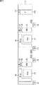
図2は、固体撮像装置1の画素2の概略平面構成を示している。図2に示すように、画素2は、赤色(Red)、緑色(GRN)、青色(Blue)のそれぞれの波長の光を光電変換する第1ないし第3光電変換部が3層に積層された光電変換領域15と、各光電変換部に対応する電荷読み出し部とから構成されている。本実施の形態においては、電荷読み出し部は、第1ないし第3光電変換部に対応した第1ないし第3画素トランジスタTrA,TrB,TrCで構成されている。本実施の形態の固体撮像装置1では、画素2において縦方向の分光がなされる。
[1-2 Outline Plane Configuration of Pixel 2]
FIG. 2 shows a schematic plan configuration of the pixel 2 of the solid-state imaging device 1. As shown in FIG. 2, the pixel 2 has first to third photoelectric conversion units that photoelectrically convert light of each wavelength of red (Red), green (GRN), and blue (Blue) stacked in three layers. The
第1ないし第3画素トランジスタTrA,TrB,TrCは、光電変換領域15の周辺に形成されており、それぞれ4つのMOS型トランジスタで構成されている。第1画素トランジスタTrAは、後述する第1光電変換部で生成、蓄積された信号電荷を画素信号として出力するもので、第1転送トランジスタTr1、リセットトランジスタTr4、増幅トランジスタTr5、及び、選択トランジスタTr6で構成されている。第2画素トランジスタTrBは、後述する第2光電変換部で生成、蓄積された信号電荷を画素信号として出力するもので、第2転送トランジスタTr2、リセットトランジスタTr7、増幅トランジスタTr8、及び、選択トランジスタTr9で構成されている。第3画素トランジスタTrCは、後述する第3光電変換部で生成、蓄積された信号電荷を画素信号として出力するもので、第3転送トランジスタTr3、リセットトランジスタTr10、増幅トランジスタTr11、及び、選択トランジスタTr12で構成されている。
The first to third pixel transistors TrA, TrB, TrC are formed in the periphery of the
リセットトランジスタTr4,Tr7,Tr10は、ソース・ドレイン領域43,44とゲート電極40とで構成されている。増幅トランジスタTr5,Tr8,Tr11は、ソース・ドレイン領域44,45、ゲート電極41とで構成されている。選択トランジスタTr6,Tr9,Tr12は、ソース・ドレイン領域45,46と、ゲート電極42とで構成されている。そしてこれらの画素トランジスタTrA,TrB,TrCにおいては、フローティングディフュージョン部FD1,FD2,FD3が対応するリセットトランジスタTr4,Tr7,Tr10の一方のソース・ドレイン領域43に接続されている。さらに、フローティングディフュージョン部FD1,FD2,FD3は、対応する増幅トランジスタTr5,Tr8,Tr11のゲート電極41に接続されている。また、リセットトランジスタTr4,Tr7,Tr10と増幅トランジスタTr5,Tr8,Tr11とで共通のソース・ドレイン領域44には、電源電圧配線Vddが接続されている。また、選択トランジスタTr6,Tr9,Tr12の一方のソース・ドレイン領域46には、選択信号配線VSLが接続されている。
The reset transistors Tr4, Tr7, Tr10 are composed of source /
[1−3 画素2の概略断面構成]
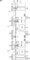
図3は、固体撮像装置1の画素2の概略断面構成を示している。図3では、第1ないし第3画素トランジスタTrA,TrB,TrCのうち第1ないし第3転送トランジスタTr1,Tr2,Tr3のみ図示し、他の画素トランジスタの図示を省略する。
[1-3 Schematic Cross-sectional Configuration of Pixel 2]
FIG. 3 shows a schematic cross-sectional configuration of the pixel 2 of the solid-state imaging device 1. In FIG. 3, only the first to third transfer transistors Tr1, Tr2, Tr3 of the first to third pixel transistors TrA, TrB, TrC are shown, and the other pixel transistors are not shown.
本実施の形態の固体撮像装置1は、半導体基板17の表面側である画素トランジスタが形成された側とは反対側の裏面側から光が入射される裏面照射型の固体撮像装置である。図3では、上側が裏面側の受光面側(光入射面側)であり、下側が表面側であり、画素トランジスタや、ロジック回路等の周辺回路などが形成された回路形成面である。
The solid-state imaging device 1 according to the present embodiment is a back-illuminated solid-state imaging device in which light is incident from the back side opposite to the side on which the pixel transistor is formed, which is the front side of the
光電変換領域15は、半導体基板17に形成される第1及び第2フォトダイオードPD1及びPD2からなる第1及び第2光電変換部と、半導体基板17の裏面側に形成された有機光電変換膜36aからなる第3光電変換部とが光の入射方向に積層された構成とされる。
The
第1及び第2フォトダイオードPD1及びPD2は、シリコンからなる半導体基板17の、第1導電型(本実施の形態ではp型とする)の半導体領域からなるウェル領域16に形成されている。第1フォトダイオードPD1は、半導体基板17の受光面側に形成された第2導電型(本実施の形態ではn型とする)不純物によるn型半導体領域19と、その一部が半導体基板の表面側に達するように延長して形成された延長部19aを有する。延長部19aは、3層の光電変換部が積層された部分で構成される光電変換領域15の周辺に形成されるもので、その延長部19aの表面(半導体基板の表面)には、ホール蓄積層となる高濃度のp型半導体領域20が形成されている。また、この延長部19aは、第1フォトダイオードのn型半導体領域19に蓄積された信号電荷を半導体基板17の表面側に抜き出すための抜き出し層として形成されるものである。
The first and second photodiodes PD1 and PD2 are formed in a
第2フォトダイオードPD2は、半導体基板17の表面側に形成されたn型半導体領域21と、その表面側の半導体基板17界面に形成されたホール蓄積層となる高濃度のp型半導体領域22とで構成されている。第1フォトダイオードPD1及び第2フォトダイオードPD2において、半導体基板17の界面にp型半導体領域20及び22が形成されることにより、半導体基板17界面で発生する暗電流の抑制が図られる。
The second photodiode PD2 includes an n-
受光面から一番離れた領域に形成された第2フォトダイオードPD2は、赤色の波長の光を光電変換する光電変換部とされる。また、受光面側に形成された第1フォトダイオードPD1は、青色の波長の光を光電変換する光電変換部とされる。 The second photodiode PD2 formed in a region farthest from the light receiving surface is a photoelectric conversion unit that photoelectrically converts light having a red wavelength. The first photodiode PD1 formed on the light receiving surface side is a photoelectric conversion unit that photoelectrically converts light having a blue wavelength.
図3の画素2において、緑色の波長の光を光電変換する光電変換部は、裏面側の半導体基板17上の有機光電変換膜36aにより構成されている。有機光電変換膜36aには、例えば、ローダーミン系色素、メラシアニン系色素、キナクリドン等を含む有機光電変換材料が用いられる。
In the pixel 2 in FIG. 3, the photoelectric conversion unit that photoelectrically converts light having a green wavelength is configured by an organic
有機光電変換膜36aの上面はパッシベーション膜(窒化膜)36bで覆われ、有機光電変換膜36aとパッシベーション膜36bが、上部電極34a及び下部電極34bで挟まれた構成とされている。
The upper surface of the organic
上部電極34aの上側には平坦化膜51が形成され、平坦化膜51の上にオンチップレンズ52が設けられる。一方、下部電極34bと同一平面で、下部電極34bが形成されていない領域には、下部電極34bのエッジの段差を緩和するための絶縁膜35が設けられる。上部電極34a及び下部電極34bは、光透過性の材料で構成され、例えば、インジウム錫(ITO)膜、酸化インジウム亜鉛膜等の透明導電膜で構成される。
A
本実施の形態では、有機光電変換膜36aの材料を緑色の光を光電変換する材料で構成したが、青色あるいは赤色の波長の光を光電変換する材料で構成し、第1フォトダイオードPD1及び第2フォトダイオードPD2をその他の波長に対応させて構成してもよい。
In the present embodiment, the organic
例えば、有機光電変換膜36aで青色の光を吸収させる場合には、半導体基板17の受光面側に形成される第1フォトダイオードPD1を、緑色の光を光電変換する光電変換部として設定し、第2フォトダイオードPD2を、赤色の光を光電変換する光電変換部として設定することができる。
For example, when blue light is absorbed by the organic
また、有機光電変換膜36aで赤色の光を吸収させる場合には、半導体基板17の受光面側に形成される第1フォトダイオードPD1を、青色の光を光電変換する光電変換部として設定し、第2フォトダイオードPD2を、緑色の光を光電変換する光電変換部として設定することができる。
When the organic
青色の光を光電変換する有機光電変換膜としては、クマリン酸色素、トリス−8−ヒドリキシキノリAl(Alq3)、メラシアニン系色素等を含む有機光電変換材料を用いることができる。また、赤色の光を光電変換する有機光電変換膜としては、フタロシアニン系色素を含む有機光電変換材料を用いることができる。 As an organic photoelectric conversion film that photoelectrically converts blue light, an organic photoelectric conversion material containing a coumaric acid dye, tris-8-hydroxyquinori Al (Alq3), a melocyanine dye, or the like can be used. Moreover, as an organic photoelectric conversion film that photoelectrically converts red light, an organic photoelectric conversion material containing a phthalocyanine dye can be used.
なお、本実施の形態のように、半導体基板17内で光電変換する光を、青色及び赤色とし、有機光電変換膜36aで光電変換する光を緑色と設定することが望ましい。第1及び第2フォトダイオードPD1,PD2間における分光特性を向上させることができるからである。
As in the present embodiment, it is desirable to set the light photoelectrically converted in the
上述の有機光電変換膜36aの半導体基板17側に形成される下部電極34bは、絶縁膜33を貫通するコンタクトプラグ32aを介して、遮光膜と配線を兼ねる導電膜32と接続されている。導電膜32には、例えばAl、Ti、W等を用いることができる。そして、導電膜32は、反射防止層30を貫通するコンタクトプラグ31を介して、半導体基板17裏面側から表面側にかけて形成された縦型転送路60の接続部23に接続されている。
The
縦型転送路60は、半導体基板17の裏面側から表面側にかけて縦方向に形成された接続部23、電位障壁層24、電荷蓄積層25、及びp型半導体領域26の積層構造により構成されている。
The
接続部23は、コンタクトプラグ31とのオーミックコンタクトのために、高不純物濃度のn型不純物領域により構成されている。電位障壁層24は、低濃度のp型不純物領域からなり、接続部23と電荷蓄積層25間においてポテンシャルバリアを構成する。電荷蓄積層25は、有機光電変換膜36aから転送された信号電荷を蓄積する層であり、接続部23よりも低濃度のn型不純物領域で構成される。半導体基板17の最表面に形成されたp型半導体領域26は、高濃度のp型不純物領域で構成され、これにより半導体基板17界面における暗電流の発生が抑制される。
The
図4を参照して、縦型転送路60について説明する。
The
図4Aは、縦型転送路60の拡大図を示し、図4Bは、図4Aにおけるx−x’線上に沿う断面構成図を示している。
4A shows an enlarged view of the
本実施の形態における縦型転送路60では、図4Bに示すようなポテンシャル勾配が形成される。このため、有機光電変換膜36aからコンタクトプラグ31等を介して接続部23に転送されてきた信号電荷eは、電位障壁層24で形成されるオーバーフローバリア(OFB)を超えて電荷蓄積層25に蓄積されていく。電荷蓄積層25に蓄積された信号電荷eが、半導体基板17の回路形成面となる表面側に読み出されることとなる。
In the
そして、半導体基板17の回路形成面となる表面側には、図2で示したように、第1フォトダイオードPD1、第2フォトダイオードPD2及び有機光電変換膜36aに対応する第1ないし第3画素トランジスタTrA,TrB,TrCが構成されている。
As shown in FIG. 2, the first to third pixels corresponding to the first photodiode PD1, the second photodiode PD2, and the organic
図3に戻り、第1転送トランジスタTr1は、第1フォトダイオードPD1の延長部19aに隣接する半導体基板17の表面側に形成されたフローティングディフュージョン部FD1と、半導体基板17上にゲート絶縁膜を介して形成された転送ゲート電極37とで構成される。第2転送トランジスタTr2は、第2フォトダイオードPD2に隣接する半導体基板17の表面側に形成されたフローティングディフュージョン部FD2と、半導体基板17上にゲート絶縁膜を介して形成された転送ゲート電極38とで構成される。第3転送トランジスタTr3は、縦型転送路60に隣接する半導体基板17の表面側に形成されたフローティングディフュージョン部FD3と、半導体基板17上にゲート絶縁膜を介して形成された転送ゲート電極39とで構成される。
Returning to FIG. 3, the first transfer transistor Tr1 includes a floating diffusion portion FD1 formed on the surface side of the
フローティングディフュージョン部FD1、FD2、及びFD3は、いずれもn型の高濃度不純物領域で構成され、転送ゲート電極37ないし39は、例えばポリシリコンで構成される。
The floating diffusion portions FD1, FD2, and FD3 are all formed of n-type high concentration impurity regions, and the
半導体基板17の表面側には、層間絶縁膜29を介して複数層(本実施の形態では3層)に積層された配線28を有する多層配線層27が形成されている。また、多層配線層27の表面には、製造段階において形成される支持基板61が形成されている。
On the surface side of the
以上のように、本実施の形態の固体撮像装置1では、画素2において縦方向に分光がなされるので、カラーフィルタは構成されていない。 As described above, in the solid-state imaging device 1 of the present embodiment, the color filter is not configured because the pixels 2 perform the spectrum in the vertical direction.
[1−4 従来の問題]
図3および図4を参照して説明した画素2の構造において、接続部23は、コンタクトプラグ31とオーミックコンタクトを取る必要があるため、高濃度のn型不純物領域とする必要がある。具体的には、1×10¹⁹ないし1×10²⁰/cm3の濃度にする必要がある。
[1-4 Conventional problems]
In the structure of the pixel 2 described with reference to FIGS. 3 and 4, the
図5を参照して、従来の接続部23の形成方法について説明する。
With reference to FIG. 5, a conventional method of forming the
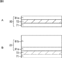
まず、図5Aに示されるようなSOI基板70が用意される。SOI基板70は、シリコンからなる支持基板71上に、BOX層72(埋め込み酸化膜)、及び、シリコンからなる半導体層73が順に積層されて構成される。SOI基板70の半導体層73が、図3の半導体基板17に対応する。半導体層73は、例えば、n型の半導体層とされ、その厚みは、例えば、3μmに形成されている。
First, an
そして、図5Bに示されるように、SOI基板70の半導体層73のBOX層72界面近傍の深い領域に、n型の不純物を高濃度にイオン注入することで、接続部23が形成される。
Then, as shown in FIG. 5B, the
その後、図5Cに示されるように、電位障壁層24、電荷蓄積層25、p型半導体領域26が、順にイオン注入により形成され、支持基板71およびBOX層72が除去された後、上下に反転された状態が、図3および図4の縦型転送路60に相当する。
Thereafter, as shown in FIG. 5C, the
従来の製造方法では、上述したように、半導体層73のBOX層72界面近傍の深い領域に、n型の不純物を高濃度にイオン注入する必要があるが、半導体層73の深い領域に、不純物濃度分布が急峻になるように接続部23を形成するのは困難であった。
In the conventional manufacturing method, as described above, it is necessary to ion-implant n-type impurities at a high concentration in a deep region near the interface of the
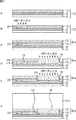
[1−5 第1の製造方法]
そこで、例えば、本実施の形態では、以下の第1ないし第4の製造方法により、高濃度の不純物領域である接続部23が形成される。
[1-5 First production method]
Thus, for example, in the present embodiment, the
以下に後述する第1ないし第4の製造方法では、最初に、図6Aに示されるように、図5Aの3μmより薄膜の半導体層81aを有するSOI基板80が用意される。SOI基板80は、支持基板71上に、BOX層72と半導体層81aが順に積層されて構成されている。なお、半導体層81aの厚みは、10ないし500nmの範囲内で適宜決定することができる。
In first to fourth manufacturing methods to be described later, first, as shown in FIG. 6A, an
そして、所定の工程後、図6Bに示されるように、エピタキシャル成長により半導体層81bが積み増しされる。図6Bの半導体層81aと81bとからなる半導体層81が、図5の半導体層73に相当する。本実施の形態では、最初に形成されるときの半導体層81aと81bの導電型は、例えば、第2導電型(n型)であるとする。
Then, after the predetermined process, as shown in FIG. 6B, the semiconductor layers 81b are stacked by epitaxial growth. The semiconductor layer 81 composed of the semiconductor layers 81a and 81b in FIG. 6B corresponds to the
図7を参照して、接続部23の第1の製造方法について説明する。
With reference to FIG. 7, the 1st manufacturing method of the
第1の製造方法では、薄膜の半導体層81a上の接続部23となる領域が開口するようにレジスト81が形成される。そして、高ドーズ量(Dose量)で照射エネルギーを高くして、イオンの注入深さRp(Projection Range)を、BOX層72界面近傍に設定し、n型不純物を高濃度にイオン注入することで、接続部23が形成される。イオンの注入深さRpは、不純物濃度分布(プロファイル)のピークとなる位置に対応する。第1の製造方法において、薄膜の半導体層81aの厚みは、例えば、200ないし300nmとし、イオンの注入深さRpは、例えば、BOX層72界面から100nm以内の範囲とすることができる。
In the first manufacturing method, the resist 81 is formed so that a region to be the
しかし、このような第1の製造方法によれば、高エネルギーのイオンにより接続部23の結晶性を破壊し、回復するのが難しい。また、高エネルギーのイオンがレジスト82にも照射されることにより、レジスト82が硬化し、剥離するのが難しくなる。
However, according to such a first manufacturing method, it is difficult to recover and destroy the crystallinity of the
[1−6 第2の製造方法]
そこで、図8Aに示す第2の製造方法のように、ドーズ量を増加させて、イオンの注入深さRpを、浅く、即ち、薄膜の半導体層81aの表面側に設定して、n型不純物を高濃度にイオン注入することで、接続部23を形成する方法もある。
[1-6 Second production method]
Therefore, as in the second manufacturing method shown in FIG. 8A, the dose is increased, and the ion implantation depth Rp is set shallow, that is, on the surface side of the
しかし、この場合には、半導体層81bを形成するための高温のエピタキシャル成長により、半導体層81aの表面の不純物濃度が上がる。そのため、図8Bに示されるように、エピタキシャル成長により形成された活性層である半導体層81bに、オートドープにより活性層が低抵抗化したオードドープ領域83が発生する。この結果、フォトダイオードのポテンシャル設計が難しくなる。さらに、エピタキシャル成長により形成された活性層である半導体層81bの、接続部23の上方部分に局所的な凹み84が発生し、STI(Shallow Trench Isolation)形成時のSiN残が発生してコンタクト形成時の問題になりやすい。
However, in this case, the impurity concentration on the surface of the
一方、オートドープを抑制できる程度の低温のエピタキシャル成長により、半導体層81bを形成した場合には、図8Cに示されるように、半導体層81b自体に結晶欠陥が生じやすい。
On the other hand, when the
また、オートドープを抑制できる程度に、ドーズ量を少なくした場合には、コンタクト抵抗が増大する。 Further, when the dose is reduced to such an extent that autodoping can be suppressed, the contact resistance increases.
従って、第1及び第2の製造方法は、従来の製造方法よりも、不純物濃度分布が急峻になるように接続部23を形成することはできるが、最良の方法とは言えない。
Therefore, the first and second manufacturing methods can form the
[1−7 第3の製造方法]
次に、図9および図10を参照して、接続部23の第3の製造方法について説明する。
[1-7 Third Production Method]
Next, with reference to FIG. 9 and FIG. 10, the 3rd manufacturing method of the
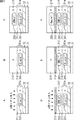
最初に、図9Aに示されるように、半導体層81a、BOX層72、及び支持基板71からなるSOI基板80上に、ハードマスクの酸化膜91が成膜される。酸化膜91は、例えば、熱酸化膜やLP-TEOSとすることができる。なお、第3の製造方法において、薄膜の半導体層81aの厚みは、例えば、200ないし300nmとすることができる。
First, as shown in FIG. 9A, a hard
次に、図9Bに示されるように、酸化膜91上にレジスト92が塗布された後、半導体層81aの接続部23となる領域が、フォトリソグラフィ及びドライエッチングにより開口される。
Next, as shown in FIG. 9B, after a resist 92 is applied on the
トレンチ(開口部)のエッチングには、例えば、枚葉のドライエッチング装置において、圧力を50ないし150mTorr、RFパワーを500ないし900W、エッチングガスとして、HBr、SF6、O2のそれぞれを100ないし300sccm、10ないし30sccm、0ないし10sccmとする条件で処理を行うことができる。ドライエッチングの後、ドライエッチングによるシリコンのダメージ除去、つまりシリコン結晶欠陥や不純物を除去する後処理が行われる。この後処理としては、例えば、ダメージレスエッチングのCDE(Chemical Dry Etching)や、アンモニアと過酸化水素水からなるHot SC1犠牲酸化処理とDHF(希フッ酸)処理を追加することが望ましい。 In the etching of the trench (opening), for example, in a single wafer dry etching apparatus, the pressure is 50 to 150 mTorr, the RF power is 500 to 900 W, the etching gas is HBr, SF 6 , and O 2 is 100 to 300 sccm The treatment can be performed under the conditions of 10 to 30 sccm and 0 to 10 sccm. After dry etching, silicon damage removal by dry etching, that is, post-processing for removing silicon crystal defects and impurities is performed. As this post-treatment, for example, CDE (Chemical Dry Etching) for damageless etching, Hot SC1 sacrificial oxidation treatment consisting of ammonia and hydrogen peroxide, and DHF (dilute hydrofluoric acid) treatment are preferably added.
次に、酸化膜91上のレジスト92が剥離された後、図9Cに示されるように、開口された半導体層81aの接続部23となる領域に、n型の不純物が高濃度にイオン注入され、接続部23が形成される。有機光電変換膜36aからの信号電荷を取り出すためのコンタクトプラグ31とオーミックコンタクトをとる必要があるため、接続部23の不純物濃度は、1×10¹⁹ないし1×10²⁰/cm3程度の濃度とされる。注入されるn型の不純物は、例えば、リン(P)やヒ素(As)とすることができる。
Next, after the resist 92 on the
次に、図10Aに示されるように、酸化膜91除去後、イオン注入により形成した接続部23の上のエッチングされた領域のみを選択した選択的低温エピタキシャル成長により、半導体層81a’(シリコン)が形成される。即ち、エッチングされた領域が、選択的低温エピタキシャル成長により、元の半導体層81aの厚みに埋め戻される。ここでの低温エピタキシャル成長の条件としては、例えば、温度を600℃ないし950℃、圧力を10Torrないし760Torr、ジクロロシラン(DCS)の流量を10ないし100sccm、塩化水素(HCl)の流量を10ないし300sccm、水素(H2)の流量を10ないし50slmとすることができる。半導体層81a’は、低温のエピタキシャル成長により形成されるため、接続部23の不純物がドープすることはない。「低温」の条件としては、上述のように950℃以下であることとするが900℃以下が望ましい。また、上記のジクロロシラン(DCS)の代わりに、SiH4,SiH3Cl,SiH2Cl2,SiHCl3,SiCl4などでもよい。なお、200nmの膜厚の半導体層81a’を、低温のエピタキシャル成長により形成するのに必要な時間は、20分程度である。
Next, as shown in FIG. 10A, after the
次に、図10Bに示されるように、半導体層81aの、水平方向の位置が接続部23と異なる領域に、リンまたはヒ素などのn型の不純物がイオン注入され、n型半導体領域19が形成される。このn型半導体領域19が、上述した第1フォトダイオードPD1を構成する。
Next, as shown in FIG. 10B, an n-type impurity such as phosphorus or arsenic is ion-implanted into a region of the
なお、図10Cに示されるように、第1フォトダイオードPD1となるn型半導体領域19とBOX層72との間の半導体層81aの領域に、p型の不純物を高濃度にイオン注入することで、ピニング層101を形成するようにしてもよい。半導体層81aにピニング層101を設けない場合には、支持基板71及びBOX層72が除去された後に成膜される反射防止層30として負の固定電荷を有する膜を用いて、ピニング膜とすることができる。負の固定電荷を持つピニング膜は、例えば、酸化ハフニウム(HfO2)、酸化アルミニウム(Al2O3)などである。ピニング層101またはピニング膜により、半導体基板17裏面側の界面にホールの蓄積状態が強化され、暗電流の発生を抑制することができる。
As shown in FIG. 10C, a p-type impurity is ion-implanted at a high concentration in the region of the
そして、最後に、図10Dに示されるように、高温のエピタキシャル成長により、n型の半導体層81bが形成される。高温のエピタキシャル成長によるn型の半導体層81bと、SOI基板80の半導体層81aとを合わせた厚みが、従来の半導体層73と同様の厚み(3μm)になるまで、半導体層81bがエピタキシャル成長される。高温のエピタキシャル成長によりn型の半導体層81bを形成しても、低温のエピタキシャル成長により形成された半導体層81a’で接続部23は覆われているため、高濃度不純物領域である接続部23の不純物がドープすることはない。
Finally, as shown in FIG. 10D, an n-
以上説明した第3の製造方法によれば、例えば、200ないし300nm程度の厚みの半導体層81aをドライエッチングによりさらに薄膜化した上で、イオン注入により接続部23となる高濃度の不純物領域が形成される。そして、形成された高濃度の不純物領域である接続部23の上部が選択的低温エピタキシャル成長により、半導体層81a’(シリコン)が積み増しされた後、高温エピタキシャル成長により、さらに、半導体層81bが積み増しされる。
According to the third manufacturing method described above, for example, the
[1−8 第4の製造方法]
次に、図11を参照して、接続部23の第4の製造方法について説明する。
[1-8 Fourth Manufacturing Method]
Next, with reference to FIG. 11, the 4th manufacturing method of the
第4の製造方法では、図11Aに示されるように、BOX層72上に形成されるn型の半導体層111の厚みが、上述したSOI基板80よりも、さらに薄膜であるSOI基板112が用いられる。n型の半導体層111の厚みは、例えば、100nm程度である。
In the fourth manufacturing method, as shown in FIG. 11A, an
そして、図11Bに示されるように、半導体層111の所定の領域に、p型の不純物が高濃度にイオン注入され、接続部23が形成される。有機光電変換膜36aからの信号電荷を取り出すためのコンタクトプラグ31とオーミックコンタクトをとる必要があるため、接続部23の不純物濃度は、1×10¹⁹ないし1×10²⁰/cm3程度の濃度とされる。注入されるp型の不純物は、例えば、リン(P)やヒ素(As)である。
Then, as shown in FIG. 11B, a p-type impurity is ion-implanted at a high concentration in a predetermined region of the
次に、図11Cに示されるように、高温のエピタキシャル成長により、第1フォトダイオードPD1となるn型半導体領域19の形成が可能となる厚みまで、具体的には、図6Aで説明した200ないし300nmの厚みとなるまで、n型の半導体層121が形成される。換言すれば、高温のエピタキシャル成長により積み増しされた半導体層121と、半導体層111とからなる半導体層によって、図6Aの半導体層81aが形成される。
Next, as shown in FIG. 11C, the thickness is such that the n-
その後の工程は、上述した第3の製造方法と同様である。即ち、図11Dに示されるように、n型の不純物が高濃度にイオン注入され、第1フォトダイオードPD1のためのn型半導体領域19が形成される。そして、図11Eに示されるように、p型のイオン注入により、ピニング層101が必要に応じて形成され、図11Fに示されるように、高温のエピタキシャル成長により、n型の半導体層81bが形成される。
The subsequent steps are the same as in the third manufacturing method described above. That is, as shown in FIG. 11D, n-type impurities are ion-implanted at a high concentration to form an n-
以上説明した第4の製造方法によれば、例えば、100nm程度の厚みの半導体層111に対して、イオン注入により接続部23としての高濃度の不純物領域が形成される。そして、半導体層111全面に対して、高温のエピタキシャル成長により半導体層121(シリコン)が積み増しされた後、高温のエピタキシャル成長により、半導体層81bが形成される。
According to the fourth manufacturing method described above, for example, a high-concentration impurity region is formed as the
第3及び第4の製造方法のいずれにおいても、高濃度の不純物領域である接続部23が形成され、BOX層72の界面が接続部23で覆われる。そして、形成された接続部23が、エピタキシャル成長により積み増した半導体層81a’または121で覆われる。さらに、接続部23が半導体層81a’または121で覆われた状態から、高温のエピタキシャル成長によりさらに半導体層81bが形成される。従って、オートドープを抑制することができる。
In both the third and fourth manufacturing methods, the
また、薄く形成された半導体層81aに対して、コンタクトプラグ31とオーミックコンタクトをとる必要がある接続部23や、第1フォトダイオードPD1となるn型半導体領域19を形成するためのイオン注入を行うことができるので、BOX層72の界面近傍に不純物濃度分布(プロファイル)のピークRpが存在する高濃度不純物領域の形成が可能となる。即ち、従来の3μm程度の厚みの半導体層73でいうところの深い領域に、不純物濃度分布(プロファイル)のピークRpが存在する接続部23とn型半導体領域19を形成することができる。これにより、オートドープの抑制とコンタクト抵抗の低減を両立させることができる。また、接続部23以外の結晶性も改善することができ、白点、暗電流特性を改善することができる。
Also, ion implantation is performed on the thinly formed
なお、不純物濃度分布(プロファイル)のピークRpが存在するBOX層72の界面近傍とは、具体的には、電位障壁層24より界面側であり、BOX層72の界面から100nm以内を意味する。
Note that the vicinity of the interface of the
[1−9 半導体基板の裏面側の製造工程]
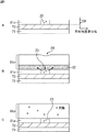
図12ないし図15を参照して、光入射面となる半導体基板17の裏面側の製造工程について、簡単に説明する。
[1-9 Manufacturing Process on Back Side of Semiconductor Substrate]
With reference to FIGS. 12 to 15, a manufacturing process on the back surface side of the
図12は、半導体層81aと81bとからなる半導体基板17に、第2フォトダイオードPD2となるn型半導体領域21、縦型転送路60を構成する電位障壁層24及び電荷蓄積層25等を形成し、素子反転して、支持基板71とBOX層72が除去された状態を示している。
In FIG. 12, the n-
なお、図12ないし図15において、図3と対応する部分については同一の符号を付してあるので、その説明は省略する。また、図12ないし図14は概略の構成であるので、図3では図示されているが、図12ないし図15では図示されていないものもある。 12 to 15, the same reference numerals are given to the portions corresponding to those in FIG. 3, and the description thereof is omitted. Also, FIGS. 12 to 14 are schematic configurations, so that they are shown in FIG. 3, but some are not shown in FIGS.
一方、図12の接続部141とコンタクトプラグ142は、図3では図示されていないので簡単に説明する。接続部141は、最終的に、上部電極34a(図3)と接続される。上部電極34aは、ホールを引き抜くので、接続部141は、高濃度のp型の不純物領域で構成される。また、コンタクトプラグ142は、半導体基板17を貫通し、上部電極34aに所定の電位を与えるための表面側の回路と接続されている。コンタクトプラグ142は、p型の不純物領域で構成することができる。
On the other hand, the
図12の状態の後、図13に示されるように、半導体基板17の裏面側に反射防止層30が形成され、接続部23および接続部141の上部にコンタクトホールが形成される。そして、形成されたコンタクトホールに導電膜を埋め込むことで、コンタクトプラグ31が形成されるとともに、反射防止層30の上面にも同一の導電膜が積層される。
After the state of FIG. 12, as shown in FIG. 13, the
反射防止層30の上面に積層された導電膜は、図14に示されるように、遮光したい領域だけを残すように加工され、遮光膜32となる。従って、遮光膜32は、配線を兼用したものとなり、コンタクトプラグ31の材料をそのまま遮光膜32として残すことで、工程を増やすことなく、コンタクトプラグ31と遮光膜32を形成することができる。コンタクトプラグ31及び遮光膜32となる導電膜には、バリアメタル膜としてチタン(Ti)と窒化チタン(TiN)の積層膜、コンタクトホールに埋め込む金属材料としては、タングステン(W)を用いることが好ましい。
As shown in FIG. 14, the conductive film laminated on the upper surface of the
次に、図15に示されるように、遮光膜32上に絶縁膜33が形成され、CMP(chemical mechanical polishing:化学的機械研磨)を用いて、絶縁膜33が平坦化される。
Next, as shown in FIG. 15, an insulating
そして、平坦化された絶縁膜33のうち、遮光膜32かつコンタクトプラグ31の上部が開口され、そこにコンタクトプラグ32aが形成された後、下部電極34bと、そのエッジの段差を緩和するための絶縁膜35が形成される。この絶縁膜35は、全面に成膜した後に、テーパ形状を持ち、下部電極34bの表面を露出するようなエッチングを行うことで形成される。
Then, in the planarized insulating
次に、緑色の光を光電変換する有機光電変換膜36a、パッシベーション膜36b、及び上部電極34aが積層される。このとき、有機光電変換膜36aとパッシベーション膜36bは、下部電極34bおよび絶縁膜35の上部の全面に形成されるが、上部電極34aは、図15で有機光電変換膜36aとパッシベーション膜36bが形成されている一部の領域のみ形成される。そして、一部の領域のみに形成された上部電極34aをハードマスクとして、有機光電変換膜36aとパッシベーション膜36bが、図15で示される領域のみにエッチングされる。その後、上部電極34aの残りの領域、即ち、図15右端の接続部141に接続する下部電極34bとその両側の絶縁膜35の上面の上部電極34aが、形成される。また、黒基準画素領域の画素については、さらに、遮光膜151も形成される。
Next, an organic
[1−10 駆動方法]
次に、固体撮像装置1の駆動方法について説明する。駆動方法については、図2及び図3を用いて説明する。
[1-10 Driving method]
Next, a method for driving the solid-state imaging device 1 will be described. The driving method will be described with reference to FIGS.
有機光電変換膜36aの受光面側に形成された上部電極34aには、固定の負電圧VLが印加され、コンタクトプラグ31に接続されている下部電極34bに電荷蓄積時において、電圧VLよりも高い電圧VHが印加されている。電圧VHはオーバーフローバリアの電位によって決定される。
A fixed negative voltage VL is applied to the
電荷蓄積時において、1つの画素2に光が入射すると、緑の波長の光は、緑の波長光に吸収特性を有する有機光電変換膜36aにおいて光電変換され、有機光電変換膜36aにおいて電子・ホール対が形成される。この光電変換により生成された電子・ホール対のうち、信号電荷となる電子が、高い電圧VHが印加されている下部電極34bに引かれ、コンタクトプラグ31を通って接続部23に転送される。そして、接続部23の飽和電荷量を超えた信号電荷は、電位障壁層24を超えて、電荷蓄積層25にオーバーフローされ、電荷蓄積層25において蓄積される。このとき、ホールは負電圧VLが印加された上部電極34aに引かれ、図示しない所要の配線を通じて排出される。また、本実施形態例においては、下部電極34bには高い電圧VHが印加されているので、半導体基板17の裏面側界面に暗電流が発生するバイアス電圧の極性に相当する。しかしながら、反射防止層30において酸化ハフニウムなどを用いることにより半導体基板17裏面にホールが励起された状態とされる。このため、下部電極34bに印加する電圧VHに起因して半導体基板17界面に発生する暗電流を抑制することができる。
When light is incident on one pixel 2 during charge accumulation, light having a green wavelength is photoelectrically converted by the organic
また、青色の波長の光は、受光面に近い半導体基板17内に形成された第1フォトダイオードPD1に吸収され光電変換される。これにより、青色の光に対応する信号電荷が第1フォトダイオードPD1のn型半導体領域19に蓄積される。赤色の波長の光は、受光面から深さ方向に深い半導体基板17内に形成された第2フォトダイオードPD2に吸収され光電変換される。これにより、赤色の光に対応する信号電荷が第2フォトダイオードPD2のn型半導体領域21に蓄積される。
The blue wavelength light is absorbed and photoelectrically converted by the first photodiode PD1 formed in the
そして、電荷蓄積が終了した後、第1ないし第3転送トランジスタTr1,Tr2,Tr3の転送ゲート電極37,38,39に所望の転送パルスが印加されることにより、電荷の読み出しが開始される。第1転送トランジスタTr1では、第1フォトダイオードPD1のn型半導体領域19に蓄積された青色の光に対応する信号電荷が延長部19aを通ってフローティングディフュージョン部FD1に読み出される。また、第2転送トランジスタTr2では、第2フォトダイオードPD2のn型半導体領域21に蓄積された赤色の光に対応する信号電荷がフローティングディフュージョン部FD2に読み出される。また、第3転送トランジスタTr3では、縦型転送路60の電荷蓄積層25に蓄積された緑色の光に対応する信号電荷がフローティングディフュージョン部FD3に読み出される。
After the charge accumulation is completed, a desired transfer pulse is applied to the
そして、それぞれの信号電荷がそれぞれのフローティングディフュージョン部FD1,FD2,FD3に読み出されることによる電位変化が増幅トランジスタTr5,Tr8,Tr11によって増幅され、画素信号とされて図示しない垂直信号配線に読み出される。垂直信号配線に読み出されるタイミングは、選択トランジスタTr6,Tr9,Tr12によって決定される。 Then, potential changes caused by reading out the respective signal charges to the respective floating diffusion portions FD1, FD2, and FD3 are amplified by the amplification transistors Tr5, Tr8, and Tr11, and are converted into pixel signals and read out to a vertical signal wiring (not shown). The timing for reading out to the vertical signal wiring is determined by the selection transistors Tr6, Tr9, Tr12.
信号電荷の読み出し、転送後は、リセットトランジスタTr4,Tr7,Tr10によって、フローティングディフュージョン部FD1,FD2,FD3に読み出された信号電荷がリセットされる。 After reading and transferring the signal charges, the reset transistors Tr4, Tr7, Tr10 reset the signal charges read to the floating diffusion portions FD1, FD2, FD3.
本実施の形態によれば、有機光電変換膜36aで生成された信号電荷を半導体基板17に形成した縦型転送路60において、接続部23から電荷蓄積層25内に縦方向にオーバーフローさせて転送し、電荷蓄積層25内に蓄積することができる。このような縦方向のオーバーフロー構造を有する縦型転送路60の形成は、上述したように、イオン注入のエネルギーによって精密に制御できるため、横方向のオーバーフロー構造よりも製造し易く、プロセスの制御性を向上させることができる。また、縦型転送路60は、半導体基板17の裏面側から表面側にかけて縦方向に形成されるため、画素サイズの増大を伴うことがなく、有機光電変換膜36aで生成された信号電荷を半導体基板17の裏面側から表面側に読み出すことができる。
According to the present embodiment, in the
また、電荷蓄積層25は転送ゲート電極39に近接して形成できることから、電荷蓄積層25からフローティングディフュージョン部FD3への転送にも有利な構成である。さらに、裏面照射型の固体撮像装置であるため、受光面となる半導体基板17の裏面側には多層配線層27が形成されないので、有機光電変換膜36aと半導体基板17に形成された第1及び第2フォトダイオードPD1,PD2とを近い距離に形成できる。これにより、有機光電変換膜36aと第1及び第2フォトダイオードPD1,PD2の距離が遠い場合に発生するF値による色毎の感度変動の影響も低減することができる。
In addition, since the
本実施の形態では、図2に示すような画素2の構成としたが、各画素トランジスタを複数の画素で共有する例としてもよい。 In this embodiment, the pixel 2 is configured as shown in FIG. 2, but each pixel transistor may be shared by a plurality of pixels.
<2.第2の実施の形態>
[3色用の光電変換部を半導体層に形成する例]
上述した第1の実施の形態では、裏面照射型で半導体基板17上に1色用の光電変換層(有機光電変換膜36a)と、半導体基板17内に2色用の光電変換層(第1及び第2フォトダイオードPD1,PD2)とからなる構造が採用された。
<2. Second Embodiment>
[Example of forming photoelectric conversion portion for three colors in semiconductor layer]
In the first embodiment described above, the back-illuminated type one-color photoelectric conversion layer (organic
しかしながら、上述した第1ないし第4の製造方法のように、エピタキシャル成長により半導体層を積み増す方法によれば、図16に示されるような3色用(3層)の光電変換層201ないし203を半導体基板17内に形成することも可能である。
However, according to the method of stacking semiconductor layers by epitaxial growth as in the first to fourth manufacturing methods described above, the three-color (three-layer) photoelectric conversion layers 201 to 203 as shown in FIG. It is also possible to form it in the
図17は、半導体基板17内に3層の光電変換層を形成する第1の製造方法を示している。
FIG. 17 shows a first manufacturing method in which three photoelectric conversion layers are formed in the
青色の光電変換層201を形成するまでの工程、即ち、SOI基板80の半導体層81aに、n型の不純物領域として青色の光電変換層201を形成するまでの工程は、上述した第3および第4の製造方法と同様であるので、その説明は省略する。
The steps until the blue
そして、n型の高濃度不純物領域として青色の光電変換層201が形成された半導体層81aに対して、図17Aに示されるように、ホウ素(B)などのp型の不純物のイオン注入が行われ、p型の高濃度不純物領域211が形成される。このp型の高濃度不純物領域211は、その上部に形成される緑色の光電変換層202と電気的に絶縁させ、混色を防止するためのものである。
Then, as shown in FIG. 17A, ion implantation of a p-type impurity such as boron (B) is performed on the
次に、図17Bに示されるように、エピタキシャル成長によりn型の半導体層212が積み増しされて形成され、そこに、p型の不純物がイオン注入されることで、半導体層212が、低濃度のp型の不純物領域とされる。
Next, as shown in FIG. 17B, the n-
次に、図17Cに示されるように、n型の不純物が高濃度にイオン注入されることにより、緑色の光電変換層202が形成される。
Next, as illustrated in FIG. 17C, the green
そして、図17Dに示されるように、図17Aと同様に、緑色の光電変換層202と、その上部に形成される赤色の光電変換層203とを電気的に絶縁させるp型の高濃度不純物領域213がイオン注入により形成される。
17D, as in FIG. 17A, a p-type high concentration impurity region that electrically insulates the green
さらに、図17Eに示されるように、エピタキシャル成長によりn型の半導体層214が積み増しされて形成され、そこに、p型の不純物がイオン注入されることで、半導体層214が、低濃度のp型の不純物領域とされる。
Further, as shown in FIG. 17E, n-type semiconductor layers 214 are formed by being epitaxially grown, and p-type impurities are ion-implanted therein, so that the
そして、図17Fに示されるように、n型の不純物が高濃度にイオン注入されることにより、赤色の光電変換層203が形成される。
Then, as shown in FIG. 17F, the red
図18は、半導体基板17内に3層の光電変換層を形成する第2の製造方法を示している。
FIG. 18 shows a second manufacturing method in which three photoelectric conversion layers are formed in the
図18Aに示される青色の光電変換層201を形成するまでの工程は、図17Aを参照して説明した方法と同様である。
The process until the blue
次に、図18Bに示されるように、エピタキシャル成長により、緑色と赤色の光電変換層202および203を形成可能な程度の厚みとなるまで、n型の半導体層221が積み増しされて形成され、そこに、p型の不純物がイオン注入されることで、半導体層221が低濃度のp型の不純物領域とされる。
Next, as shown in FIG. 18B, n-type semiconductor layers 221 are stacked and formed by epitaxial growth until the thickness is such that green and red photoelectric conversion layers 202 and 203 can be formed. , P-type impurities are ion-implanted, so that the
以下、図17Cないし図17Fを参照して説明した方法と同様の方法で、順次、緑色の光電変換層202、p型の高濃度不純物領域213、赤色の光電変換層203が形成され、図18Cに示されるように、3色の光電変換層201、202、および203が形成される。
Thereafter, a green
以上のように、エピタキシャル成長により半導体層を積み増す方法によって、3層の光電変換層を半導体基板17内に形成することも可能である。エピタキシャル成長により半導体層を積み増し、複数の光電変換層を半導体基板17内に形成する方法は、上述した裏面照射型の固体撮像装置のほか、表面照射型の固体撮像装置であっても適用可能である。
As described above, it is possible to form three photoelectric conversion layers in the
上述した実施の形態では、第1に、SOI基板80,112の予め形成された半導体層81a,111に、高濃度の不純物をイオン注入して、接続部23およびn型半導体領域19が形成される。そして、第2に、エピタキシャル成長により半導体層81bが積み増しされる。これにより、半導体層の光入射面から浅い領域に、不純物濃度分布のピークRpを有する高濃度不純物領域を形成することができる。
In the above-described embodiment, first, the
なお、上述した実施の形態では、半導体基板としてSOI基板(80,112)を採用した例について説明した。しかし、BOX層72に代わりに、ホウ素(B)やアンチモン(Sb)などのドープ層でもよい。また、ドープ層がなくてもよい。
In the above-described embodiment, the example in which the SOI substrate (80, 112) is employed as the semiconductor substrate has been described. However, instead of the
また、上述した実施の形態では、半導体層の光入射面から浅い領域にある高濃度不純物領域の例として、接続部23およびn型半導体領域19を説明したが、その他の領域にも適用できることは言うまでもない。例えば、上部電極34aと接続される接続部141(図15)や、画素領域3以外の周辺回路のコンタクトの形成にも適用することができる。
In the above-described embodiment, the
さらに、上述した実施形態では、電子を信号電荷としたもので、第1導電型をp型、第2導電型をn型としているが、本技術は正孔を信号電荷とする固体撮像装置にも適用することができる。すなわち、第1導電型をn型とし、第2導電型をp型として、前述の各半導体領域を逆の導電型の半導体領域で構成することができる。 Furthermore, in the above-described embodiment, electrons are used as signal charges, and the first conductivity type is p-type and the second conductivity type is n-type. However, the present technology is applied to a solid-state imaging device using holes as signal charges. Can also be applied. That is, the first conductivity type can be an n-type, the second conductivity type can be a p-type, and each of the semiconductor regions described above can be composed of semiconductor regions of opposite conductivity types.
また、本技術は、可視光の入射光量の分布を検知して画像として撮像する固体撮像装置への適用に限らず、赤外線やX線、あるいは粒子等の入射量の分布を画像として撮像する固体撮像装置にも適用可能である。また、広義の意味として、圧力や静電容量など、他の物理量の分布を検知して画像として撮像する指紋検出センサ等の固体撮像装置(物理量分布検知装置)全般に対して適用可能である。 In addition, the present technology is not limited to application to a solid-state imaging device that detects the distribution of the amount of incident light of visible light and captures it as an image, but is a solid that captures the distribution of the incident amount of infrared rays, X-rays, or particles as an image. The present invention can also be applied to an imaging device. In a broad sense, the present invention can be applied to all solid-state imaging devices (physical quantity distribution detection devices) such as a fingerprint detection sensor that senses other physical quantity distributions such as pressure and capacitance and captures images as images.
さらに、本技術は、画素部の各単位画素を行単位で順に走査して各単位画素から画素信号を読み出す固体撮像装置に限られるものではない。画素単位で任意の画素を選択して、当該選択画素から画素単位で信号を読み出すX−Yアドレス型の固体撮像装置に対しても適用可能である。なお、固体撮像装置はワンチップとして形成された形態であってもよいし、画素部と、信号処理部または光学系とがまとめてパッケージングされた撮像機能を有するモジュール状の形態であってもよい。 Furthermore, the present technology is not limited to the solid-state imaging device that sequentially scans each unit pixel of the pixel unit in units of rows and reads a pixel signal from each unit pixel. The present invention is also applicable to an XY address type solid-state imaging device that selects an arbitrary pixel in pixel units and reads out signals from the selected pixels in pixel units. Note that the solid-state imaging device may be formed as a single chip, or may be in a modular form having an imaging function in which a pixel portion and a signal processing portion or an optical system are packaged together. Good.
また、本技術は、固体撮像装置への適用に限られるものではなく、撮像装置にも適用可能である。ここで、撮像装置とは、デジタルスチルカメラやビデオカメラ等のカメラシステムや、携帯電話機などの撮像機能を有する電子機器のことを言う。なお、電子機器に搭載される上記モジュール状の形態、即ちカメラモジュールを撮像装置とする場合もある。 Further, the present technology is not limited to application to a solid-state imaging device, and can also be applied to an imaging device. Here, the imaging apparatus refers to a camera system such as a digital still camera or a video camera, or an electronic device having an imaging function such as a mobile phone. Note that the above-described module form mounted on an electronic device, that is, a camera module may be used as an imaging device.
<3.第3の実施の形態>
次に、第3の実施形態に係る電子機器について説明する。
<3. Third Embodiment>
Next, an electronic apparatus according to the third embodiment will be described.
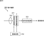
図19は、本技術が適用された第3の実施の形態に係る電子機器300の概略構成図である。 FIG. 19 is a schematic configuration diagram of an electronic apparatus 300 according to the third embodiment to which the present technology is applied.
図19の電子機器300は、上述した第1の実施形態における固体撮像装置1を電子機器(カメラ)に用いており、固体撮像装置1と、光学レンズ310と、シャッタ装置311と、駆動回路312と、信号処理回路313とを有する。
An electronic device 300 in FIG. 19 uses the solid-state imaging device 1 in the first embodiment described above as an electronic device (camera). The solid-state imaging device 1, the
光学レンズ310は、被写体からの像光(入射光)を固体撮像装置1の撮像面上に結像させる。これにより固体撮像装置1内に一定期間当該信号電荷が蓄積される。シャッタ装置311は、固体撮像装置1への光照射期間および遮光期間を制御する。駆動回路312は、固体撮像装置1の転送動作およびシャッタ装置311のシャッタ動作を制御する駆動信号を供給する。駆動回路312から供給される駆動信号(タイミング信号)により、固体撮像装置1の信号転送を行う。信号処理回路313は、各種の信号処理を行う。信号処理が行われた撮像信号は、メモリなどの記憶媒体に記憶され、あるいはモニタに出力される。
The
本実施の形態の電子機器300では、固体撮像装置1において画素サイズを微細化及び転送効率が向上されるので、画素特性が向上する。固体撮像装置1を適用できる電子機器300としては、カメラに限られるものではなく、デジタルスチルカメラ、さらには携帯電話機等のモバイル機器向けカメラモジュールなどの撮像装置に適用可能である。 In the electronic apparatus 300 according to the present embodiment, the pixel size is reduced in the solid-state imaging device 1 and the transfer efficiency is improved, so that the pixel characteristics are improved. The electronic device 300 to which the solid-state imaging device 1 can be applied is not limited to a camera, and can be applied to an imaging device such as a digital still camera and a camera module for mobile devices such as a mobile phone.
本技術の実施の形態は、上述した実施の形態に限定されるものではなく、本技術の要旨を逸脱しない範囲において種々の変更が可能である。 Embodiments of the present technology are not limited to the above-described embodiments, and various modifications can be made without departing from the gist of the present technology.
なお、本技術は以下のような構成も取ることができる。
(1)
裏面側が光入射面とされ、表面側が回路形成面とされた半導体基板と、
前記裏面側の前記半導体基板上で生成された信号電荷を前記半導体基板内に転送するコンタクトプラグと接続される接続部であって、前記裏面側の前記半導体基板の界面近傍に不純物濃度分布のピークを有する接続部と、
前記半導体基板内に形成された1以上の第1光電変換部と
を備える固体撮像装置。
(2)
前記光入射面側の前記半導体基板上に積層され、下部電極及び上部電極で挟持された第1色用の第2光電変換部をさらに備え、
前記1以上の第1光電変換部は、前記半導体基板の深さ方向に積層された、第2色用の光電変換部と第3色用の光電変換部とからなり、
前記接続部には、前記第1色用の第2光電変換部で生成された前記信号電荷が供給される
前記(1)に記載の固体撮像装置。
(3)
前記接続部は、第1の厚みの半導体層の第1の領域を選択的にエッチングして第2の厚みにした後、不純物をイオン注入することにより形成され、
前記イオン注入後に、エッチングされた前記第1の領域がエピタキシャル成長により前記第1の厚みに埋め戻された後、前記第1の厚みの半導体層が、エピタキシャル成長により第3の厚みにさらに積み増しされて、前記半導体基板とされる
前記(1)または(2)に記載の固体撮像装置。
(4)
エピタキシャル成長により前記第1の厚みに埋め戻された後、前記第1の厚みの半導体層の、水平方向の位置が前記接続部と異なる第2の領域に、1つの前記第1光電変換部が形成される
前記(3)に記載の固体撮像装置。
(5)
前記接続部は、第1の厚みの半導体層の第1の領域に対して、不純物をイオン注入することにより形成され、
前記イオン注入後に、前記第1の厚みの半導体層が、エピタキシャル成長により第2の厚みに積み増しされ、
前記第2の厚みの半導体層が、さらに、エピタキシャル成長により第3の厚みに積み増しされて、前記半導体基板とされる
前記(1)乃至(4)のいずれかに記載の固体撮像装置。
(6)
エピタキシャル成長により前記第2の厚みに積み増しされた後、前記第2の厚みの半導体層の、水平方向の位置が前記接続部と異なる第2の領域に、1つの前記第1光電変換部が形成される
前記(5)に記載の固体撮像装置。
(7)
前記不純物濃度分布のピークが、前記裏面側の前記半導体基板の界面から100nm以内の位置にある
前記(1)乃至(6)のいずれかに記載の固体撮像装置。
(8)
第1の厚みの半導体基板の第1の領域に不純物をイオン注入することにより、前記半導体基板の光入射面となる裏面側で生成された信号電荷を前記半導体基板内に転送するコンタクトプラグと接続される接続部であって、前記裏面側の前記半導体基板の界面近傍に不純物濃度分布のピークを有する接続部を形成する接続部形成工程と、
前記第1の厚みの半導体基板をエピタキシャル成長により第2の厚さまで積み増す第1の半導体層形成工程と、
前記第2の厚みの半導体基板の、前記接続部と水平方向の位置が異なる第2の領域に、第1の波長の光を光電変換する第1の光電変換層を形成する第1の光電変換層形成工程と、
前記第2の厚みの半導体基板を、エピタキシャル成長により、第3の厚みまで積み増す第2の半導体層形成工程と
を含む固体撮像装置の製造方法。
(9)
前記接続部形成工程は、前記第1の厚みより厚い第4の厚みから選択的にエッチングされ前記第1の厚みとされた前記半導体基板の前記第1の領域に不純物をイオン注入することにより、前記接続部を形成し、
前記第1の半導体層形成工程は、前記イオン注入後に、エッチングされた前記第1の領域を、エピタキシャル成長により前記第1の厚みと同じ前記第2の厚さに埋め戻す
前記(8)に記載の固体撮像装置の製造方法。
(10)
前記第3の厚みの半導体基板の、前記第1の光電変換層よりも前記裏面側から離れた深さ方向の位置に、第2の波長の光を光電変換する第2の光電変換層を形成する第2の光電変換層形成工程をさらに備える
前記(8)または(9)のいずれかに記載の固体撮像装置の製造方法。
(11)
光学レンズで集光された光が入射される固体撮像装置と、
前記固体撮像装置の出力信号を処理する信号処理回路と
を備え、
前記固体撮像装置は、
裏面側が光入射面とされ、表面側が回路形成面とされた半導体基板と、
前記裏面側の前記半導体基板上で生成された信号電荷を前記半導体基板内に転送するコンタクトプラグと接続される接続部であって、前記裏面側の前記半導体基板の界面近傍に不純物濃度分布のピークを有する接続部と、
前記半導体基板内に形成された1以上の光電変換部と
を備える電子機器。
In addition, this technique can also take the following structures.
(1)
A semiconductor substrate whose back side is a light incident surface and whose front side is a circuit forming surface;
A connection portion connected to a contact plug for transferring the signal charge generated on the semiconductor substrate on the back surface side into the semiconductor substrate, and a peak of impurity concentration distribution near the interface of the semiconductor substrate on the back surface side A connection having
A solid-state imaging device comprising: one or more first photoelectric conversion units formed in the semiconductor substrate.
(2)
A second photoelectric conversion unit for the first color, which is laminated on the semiconductor substrate on the light incident surface side and sandwiched between the lower electrode and the upper electrode;
The one or more first photoelectric conversion units include a second color photoelectric conversion unit and a third color photoelectric conversion unit, which are stacked in the depth direction of the semiconductor substrate.
The solid-state imaging device according to (1), wherein the signal charge generated by the second photoelectric conversion unit for the first color is supplied to the connection unit.
(3)
The connecting portion is formed by ion-implanting impurities after selectively etching the first region of the first-thickness semiconductor layer to the second thickness,
After the ion implantation, the etched first region is backfilled to the first thickness by epitaxial growth, and then the semiconductor layer of the first thickness is further stacked to a third thickness by epitaxial growth, The solid-state imaging device according to (1) or (2), wherein the solid-state imaging device is used as the semiconductor substrate.
(4)
After being backfilled to the first thickness by epitaxial growth, one first photoelectric conversion unit is formed in a second region where the horizontal position of the semiconductor layer of the first thickness is different from the connection unit. The solid-state imaging device according to (3).
(5)
The connection portion is formed by ion-implanting impurities into the first region of the first thickness semiconductor layer;
After the ion implantation, the first-thickness semiconductor layer is stacked to a second thickness by epitaxial growth,
The solid-state imaging device according to any one of (1) to (4), wherein the semiconductor layer having the second thickness is further stacked to a third thickness by epitaxial growth to be the semiconductor substrate.
(6)
After being stacked to the second thickness by epitaxial growth, one first photoelectric conversion unit is formed in a second region where the horizontal position of the semiconductor layer of the second thickness is different from the connection unit. The solid-state imaging device according to (5).
(7)
The solid-state imaging device according to any one of (1) to (6), wherein the peak of the impurity concentration distribution is at a position within 100 nm from the interface of the semiconductor substrate on the back surface side.
(8)
Impurities are ion-implanted into the first region of the semiconductor substrate having the first thickness, thereby connecting to a contact plug that transfers signal charges generated on the back surface side, which is the light incident surface of the semiconductor substrate, into the semiconductor substrate. A connecting portion forming step of forming a connecting portion having a peak of impurity concentration distribution in the vicinity of the interface of the semiconductor substrate on the back surface side,
A first semiconductor layer forming step of stacking the semiconductor substrate having the first thickness to a second thickness by epitaxial growth;
First photoelectric conversion for forming a first photoelectric conversion layer for photoelectrically converting light of a first wavelength in a second region of the second thickness semiconductor substrate having a horizontal position different from that of the connection portion. A layer forming step;
And a second semiconductor layer forming step of increasing the semiconductor substrate having the second thickness to a third thickness by epitaxial growth.
(9)
In the connecting portion forming step, impurities are ion-implanted into the first region of the semiconductor substrate that is selectively etched from the fourth thickness that is thicker than the first thickness and is set to the first thickness, Forming the connecting portion;
The said 1st semiconductor layer formation process backfills the said 1st area | region etched after the said ion implantation to the said 2nd thickness same as the said 1st thickness by epitaxial growth. Said (8). Manufacturing method of solid-state imaging device.
(10)
A second photoelectric conversion layer that photoelectrically converts light of the second wavelength is formed at a position in the depth direction of the third thickness semiconductor substrate that is farther from the back surface side than the first photoelectric conversion layer. The manufacturing method of the solid-state imaging device in any one of said (8) or (9) further provided with the 2nd photoelectric converting layer formation process to do.
(11)
A solid-state imaging device on which the light condensed by the optical lens is incident;
A signal processing circuit for processing an output signal of the solid-state imaging device,
The solid-state imaging device
A semiconductor substrate whose back side is a light incident surface and whose front side is a circuit forming surface;
A connection portion connected to a contact plug for transferring the signal charge generated on the semiconductor substrate on the back surface side into the semiconductor substrate, and a peak of impurity concentration distribution near the interface of the semiconductor substrate on the back surface side A connection having
An electronic apparatus comprising: one or more photoelectric conversion units formed in the semiconductor substrate.
1 固体撮像装置, 2 画素, 3 画素領域, 16 ウェル領域, 17 半導体基板(半導体層), 19 n型半導体領域, 20 p型半導体領域, 21 n型半導体領域, PD1 第1フォトダイオード, PD2 第2フォトダイオード, 23 接続部, 34a 上部電極, 34b 下部電極, 36a 有機光電変換膜, 36b パッシベーション膜, 31 コンタクトプラグ, 32 遮光膜, 32a コンタクトプラグ, 300 電子機器, 310 光学レンズ, 313 信号処理回路 1 solid-state imaging device, 2 pixels, 3 pixel region, 16 well region, 17 semiconductor substrate (semiconductor layer), 19 n type semiconductor region, 20 p type semiconductor region, 21 n type semiconductor region, PD1 first photodiode, PD2 first 2 photodiodes, 23 connection part, 34a upper electrode, 34b lower electrode, 36a organic photoelectric conversion film, 36b passivation film, 31 contact plug, 32 light shielding film, 32a contact plug, 300 electronic device, 310 optical lens, 313 signal processing circuit
Claims (11)
前記裏面側の前記半導体基板上で生成された信号電荷を前記半導体基板内に転送するコンタクトプラグと接続される接続部であって、前記裏面側の前記半導体基板の界面近傍に不純物濃度分布のピークを有する接続部と、
前記半導体基板内に形成された1以上の第1光電変換部と
を備える固体撮像装置。 A semiconductor substrate whose back side is a light incident surface and whose front side is a circuit forming surface;
A connection portion connected to a contact plug for transferring the signal charge generated on the semiconductor substrate on the back surface side into the semiconductor substrate, and a peak of impurity concentration distribution near the interface of the semiconductor substrate on the back surface side A connection having
A solid-state imaging device comprising: one or more first photoelectric conversion units formed in the semiconductor substrate.
前記1以上の第1光電変換部は、前記半導体基板の深さ方向に積層された、第2色用の光電変換部と第3色用の光電変換部とからなり、
前記接続部には、前記第1色用の第2光電変換部で生成された前記信号電荷が供給される
請求項1に記載の固体撮像装置。 A second photoelectric conversion unit for the first color, which is laminated on the semiconductor substrate on the light incident surface side and sandwiched between the lower electrode and the upper electrode;
The one or more first photoelectric conversion units include a second color photoelectric conversion unit and a third color photoelectric conversion unit, which are stacked in the depth direction of the semiconductor substrate.
The solid-state imaging device according to claim 1, wherein the signal charges generated by the second photoelectric conversion unit for the first color are supplied to the connection unit.
前記イオン注入後に、エッチングされた前記第1の領域がエピタキシャル成長により前記第1の厚みに埋め戻された後、前記第1の厚みの半導体層が、エピタキシャル成長により第3の厚みにさらに積み増しされて、前記半導体基板とされる
請求項1に記載の固体撮像装置。 The connecting portion is formed by ion-implanting impurities after selectively etching the first region of the first-thickness semiconductor layer to the second thickness,
After the ion implantation, the etched first region is backfilled to the first thickness by epitaxial growth, and then the semiconductor layer of the first thickness is further stacked to a third thickness by epitaxial growth, The solid-state imaging device according to claim 1, wherein the solid-state imaging device is the semiconductor substrate.
請求項3に記載の固体撮像装置。 After being backfilled to the first thickness by epitaxial growth, one first photoelectric conversion unit is formed in a second region where the horizontal position of the semiconductor layer of the first thickness is different from the connection unit. The solid-state imaging device according to claim 3.
前記イオン注入後に、前記第1の厚みの半導体層が、エピタキシャル成長により第2の厚みに積み増しされ、
前記第2の厚みの半導体層が、さらに、エピタキシャル成長により第3の厚みに積み増しされて、前記半導体基板とされる
請求項1に記載の固体撮像装置。 The connection portion is formed by ion-implanting impurities into the first region of the first thickness semiconductor layer;
After the ion implantation, the first-thickness semiconductor layer is stacked to a second thickness by epitaxial growth,
The solid-state imaging device according to claim 1, wherein the semiconductor layer having the second thickness is further stacked to a third thickness by epitaxial growth to form the semiconductor substrate.
請求項5に記載の固体撮像装置。 After being stacked to the second thickness by epitaxial growth, one first photoelectric conversion unit is formed in a second region where the horizontal position of the semiconductor layer of the second thickness is different from the connection unit. The solid-state imaging device according to claim 5.
請求項1に記載の固体撮像装置。 The solid-state imaging device according to claim 1, wherein the peak of the impurity concentration distribution is at a position within 100 nm from the interface of the semiconductor substrate on the back surface side.
前記第1の厚みの半導体基板をエピタキシャル成長により第2の厚さまで積み増す第1の半導体層形成工程と、
前記第2の厚みの半導体基板の、前記接続部と水平方向の位置が異なる第2の領域に、第1の波長の光を光電変換する第1の光電変換層を形成する第1の光電変換層形成工程と、
前記第2の厚みの半導体基板を、エピタキシャル成長により、第3の厚みまで積み増す第2の半導体層形成工程と
を含む固体撮像装置の製造方法。 Impurities are ion-implanted into the first region of the semiconductor substrate having the first thickness, thereby connecting to a contact plug that transfers signal charges generated on the back surface side, which is the light incident surface of the semiconductor substrate, into the semiconductor substrate. A connecting portion forming step of forming a connecting portion having a peak of impurity concentration distribution in the vicinity of the interface of the semiconductor substrate on the back surface side,
A first semiconductor layer forming step of stacking the semiconductor substrate having the first thickness to a second thickness by epitaxial growth;
First photoelectric conversion for forming a first photoelectric conversion layer for photoelectrically converting light of a first wavelength in a second region of the second thickness semiconductor substrate having a horizontal position different from that of the connection portion. A layer forming step;
And a second semiconductor layer forming step of increasing the semiconductor substrate having the second thickness to a third thickness by epitaxial growth.
前記第1の半導体層形成工程は、前記イオン注入後に、エッチングされた前記第1の領域を、エピタキシャル成長により前記第1の厚みと同じ前記第2の厚さに埋め戻す
請求項8に記載の固体撮像装置の製造方法。 In the connecting portion forming step, impurities are ion-implanted into the first region of the semiconductor substrate that is selectively etched from the fourth thickness that is thicker than the first thickness and is set to the first thickness, Forming the connecting portion;
9. The solid according to claim 8, wherein in the first semiconductor layer forming step, after the ion implantation, the etched first region is backfilled to the second thickness same as the first thickness by epitaxial growth. Manufacturing method of imaging apparatus.
請求項8に記載の固体撮像装置の製造方法。 A second photoelectric conversion layer that photoelectrically converts light of the second wavelength is formed at a position in the depth direction of the third thickness semiconductor substrate that is farther from the back surface side than the first photoelectric conversion layer. The manufacturing method of the solid-state imaging device according to claim 8, further comprising: a second photoelectric conversion layer forming step.
前記固体撮像装置の出力信号を処理する信号処理回路と
を備え、
前記固体撮像装置は、
裏面側が光入射面とされ、表面側が回路形成面とされた半導体基板と、
前記裏面側の前記半導体基板上で生成された信号電荷を前記半導体基板内に転送するコンタクトプラグと接続される接続部であって、前記裏面側の前記半導体基板の界面近傍に不純物濃度分布のピークを有する接続部と、
前記半導体基板内に形成された1以上の光電変換部と
を備える電子機器。 A solid-state imaging device on which the light condensed by the optical lens is incident;
A signal processing circuit for processing an output signal of the solid-state imaging device,
The solid-state imaging device
A semiconductor substrate whose back side is a light incident surface and whose front side is a circuit forming surface;
A connection portion connected to a contact plug for transferring the signal charge generated on the semiconductor substrate on the back surface side into the semiconductor substrate, and a peak of impurity concentration distribution near the interface of the semiconductor substrate on the back surface side A connection having
An electronic apparatus comprising: one or more photoelectric conversion units formed in the semiconductor substrate.
Priority Applications (3)
| Application Number | Priority Date | Filing Date | Title |
|---|---|---|---|
| JP2011143581A JP2013012556A (en) | 2011-06-28 | 2011-06-28 | Solid-state image pickup device, manufacturing method of the same and electronic apparatus |
| CN201210206114.2A CN102856333B (en) | 2011-06-28 | 2012-06-18 | Solid camera head, its manufacture method and electronic equipment |
| US13/527,713 US9202839B2 (en) | 2011-06-28 | 2012-06-20 | Solid-state imaging device, method for manufacturing the same, and electronic apparatus to form high-concentration impurity region in semiconductor substrate |
Applications Claiming Priority (1)
| Application Number | Priority Date | Filing Date | Title |
|---|---|---|---|
| JP2011143581A JP2013012556A (en) | 2011-06-28 | 2011-06-28 | Solid-state image pickup device, manufacturing method of the same and electronic apparatus |
Publications (2)
| Publication Number | Publication Date |
|---|---|
| JP2013012556A true JP2013012556A (en) | 2013-01-17 |
| JP2013012556A5 JP2013012556A5 (en) | 2014-07-31 |
Family
ID=47389735
Family Applications (1)
| Application Number | Title | Priority Date | Filing Date |
|---|---|---|---|
| JP2011143581A Abandoned JP2013012556A (en) | 2011-06-28 | 2011-06-28 | Solid-state image pickup device, manufacturing method of the same and electronic apparatus |
Country Status (3)
| Country | Link |
|---|---|
| US (1) | US9202839B2 (en) |
| JP (1) | JP2013012556A (en) |
| CN (1) | CN102856333B (en) |
Cited By (15)
| Publication number | Priority date | Publication date | Assignee | Title |
|---|---|---|---|---|
| KR20140113098A (en) * | 2013-03-15 | 2014-09-24 | 삼성전자주식회사 | Image sensor and method of forming the same |
| JP5604703B1 (en) * | 2013-09-10 | 2014-10-15 | 弘一 関根 | Solid-state imaging device |
| JP2014199898A (en) * | 2013-03-11 | 2014-10-23 | ソニー株式会社 | Solid-state imaging element and method of manufacturing the same, and electronic equipment |
| JP2015037121A (en) * | 2013-08-13 | 2015-02-23 | 株式会社東芝 | Solid state image pickup element |
| JP2015038931A (en) * | 2013-08-19 | 2015-02-26 | ソニー株式会社 | Solid-state imaging element and electronic device |
| WO2016076138A1 (en) * | 2014-11-14 | 2016-05-19 | ソニー株式会社 | Solid-state imaging element, manufacturing method, and electronic device |
| WO2016103315A1 (en) * | 2014-12-22 | 2016-06-30 | オリンパス株式会社 | Solid-state image pickup device, and image pickup device |
| WO2016194653A1 (en) * | 2015-06-05 | 2016-12-08 | ソニー株式会社 | Imaging element, electronic device, and manufacturing device and method |
| JP2017112376A (en) * | 2015-12-15 | 2017-06-22 | 三星電子株式会社Samsung Electronics Co.,Ltd. | Image sensor and method of manufacturing the same |
| JP2017183562A (en) * | 2016-03-31 | 2017-10-05 | ソニー株式会社 | Solid-state imaging device, and electronic apparatus |
| WO2019044103A1 (en) * | 2017-08-31 | 2019-03-07 | ソニーセミコンダクタソリューションズ株式会社 | Imaging element, laminated imaging element, and solid-state imaging device |
| WO2019097971A1 (en) * | 2017-11-14 | 2019-05-23 | マッハコーポレーション株式会社 | Solid-state imaging element and method for forming same |
| JPWO2018169009A1 (en) * | 2017-03-16 | 2020-01-16 | シャープ株式会社 | Imaging device and X-ray imaging device |
| JP2021100253A (en) * | 2018-12-27 | 2021-07-01 | 株式会社ニコン | Image pickup device and image pickup apparatus |
| US11973103B2 (en) | 2016-03-31 | 2024-04-30 | Sony Group Corporation | Solid-state imaging element and electronic device |
Families Citing this family (14)
| Publication number | Priority date | Publication date | Assignee | Title |
|---|---|---|---|---|
| JP6095258B2 (en) * | 2011-05-27 | 2017-03-15 | キヤノン株式会社 | Solid-state imaging device and imaging system using solid-state imaging device |
| JP6018376B2 (en) * | 2011-12-05 | 2016-11-02 | キヤノン株式会社 | Solid-state imaging device and camera |
| US20140077324A1 (en) * | 2012-09-20 | 2014-03-20 | Sony Corporation | Solid-state image pickup device, method of manufacturing solid-state image pickup device, and electronic apparatus |
| JP6171997B2 (en) * | 2014-03-14 | 2017-08-02 | ソニー株式会社 | Solid-state imaging device, driving method thereof, and electronic apparatus |
| JP6541313B2 (en) * | 2014-07-31 | 2019-07-10 | キヤノン株式会社 | Photoelectric conversion device and imaging system |
| KR102346956B1 (en) * | 2014-08-01 | 2022-01-03 | 삼성전자주식회사 | Image sensor and electronic device including the same |
| KR102356695B1 (en) * | 2014-08-18 | 2022-01-26 | 삼성전자주식회사 | Image sensor having light guide members |
| JP6764571B2 (en) * | 2015-03-12 | 2020-10-07 | ソニー株式会社 | Solid-state image sensor, image sensor, and electronic equipment |
| JP6711573B2 (en) * | 2015-08-10 | 2020-06-17 | ソニーセミコンダクタソリューションズ株式会社 | Solid-state image sensor |
| US20200127039A1 (en) * | 2017-01-24 | 2020-04-23 | Sony Semiconductor Solutions Corporation | Light-receiving device, method of manufacturing light receiving device, imaging device, and electronic apparatus |
| JP7090087B2 (en) * | 2017-08-16 | 2022-06-23 | ソニーグループ株式会社 | Image sensor, stacked image sensor and solid-state image sensor |
| KR20210098208A (en) | 2020-01-31 | 2021-08-10 | 삼성전자주식회사 | Image sensor and electronic device |
| CN111785748A (en) * | 2020-08-10 | 2020-10-16 | 联合微电子中心有限责任公司 | Method and structure for reducing dark current of back-illuminated image sensor |
| CN117596908B (en) * | 2024-01-19 | 2024-04-05 | 武汉楚兴技术有限公司 | Pixel unit, image sensor and manufacturing method thereof |
Family Cites Families (4)
| Publication number | Priority date | Publication date | Assignee | Title |
|---|---|---|---|---|
| US6930336B1 (en) * | 2001-06-18 | 2005-08-16 | Foveon, Inc. | Vertical-color-filter detector group with trench isolation |
| JP4799835B2 (en) | 2004-07-09 | 2011-10-26 | 東レ・ダウコーニング株式会社 | Room temperature curable organopolysiloxane composition and electrical / electronic equipment |
| JP4839008B2 (en) * | 2005-03-28 | 2011-12-14 | 富士フイルム株式会社 | Single-plate color solid-state image sensor |
| JP5564847B2 (en) * | 2009-07-23 | 2014-08-06 | ソニー株式会社 | SOLID-STATE IMAGING DEVICE, ITS MANUFACTURING METHOD, AND ELECTRONIC DEVICE |
-
2011
- 2011-06-28 JP JP2011143581A patent/JP2013012556A/en not_active Abandoned
-
2012
- 2012-06-18 CN CN201210206114.2A patent/CN102856333B/en active Active
- 2012-06-20 US US13/527,713 patent/US9202839B2/en active Active
Cited By (39)
| Publication number | Priority date | Publication date | Assignee | Title |
|---|---|---|---|---|
| JP2014199898A (en) * | 2013-03-11 | 2014-10-23 | ソニー株式会社 | Solid-state imaging element and method of manufacturing the same, and electronic equipment |
| KR102214822B1 (en) * | 2013-03-11 | 2021-02-09 | 소니 주식회사 | Solid-state imaging device, method of manufacturing the same, and electronic apparatus |
| KR20150130266A (en) * | 2013-03-11 | 2015-11-23 | 소니 주식회사 | Solid-state imaging device, method of manufacturing the same, and electronic apparatus |
| KR102083550B1 (en) * | 2013-03-15 | 2020-04-14 | 삼성전자주식회사 | Image sensor and method of forming the same |
| KR20140113098A (en) * | 2013-03-15 | 2014-09-24 | 삼성전자주식회사 | Image sensor and method of forming the same |
| JP2015037121A (en) * | 2013-08-13 | 2015-02-23 | 株式会社東芝 | Solid state image pickup element |
| US11862655B2 (en) | 2013-08-19 | 2024-01-02 | Sony Group Corporation | Solid-state imaging device having through electrode provided therein and electronic apparatus incorporating the solid-state imaging device |
| JP2015038931A (en) * | 2013-08-19 | 2015-02-26 | ソニー株式会社 | Solid-state imaging element and electronic device |
| WO2015025723A1 (en) * | 2013-08-19 | 2015-02-26 | ソニー株式会社 | Solid-state imaging element and electronic device |
| US9698188B2 (en) | 2013-08-19 | 2017-07-04 | Sony Corporation | Solid-state imaging device and electronic apparatus |
| WO2015037547A1 (en) * | 2013-09-10 | 2015-03-19 | Sekine Hirokazu | Solid-state imaging device |
| JP2015056408A (en) * | 2013-09-10 | 2015-03-23 | 関根 弘一 | Solid-state image pickup device |
| US10008521B2 (en) | 2013-09-10 | 2018-06-26 | Setech Co., Ltd. | Solid-state imaging device |
| JP5604703B1 (en) * | 2013-09-10 | 2014-10-15 | 弘一 関根 | Solid-state imaging device |
| WO2016076138A1 (en) * | 2014-11-14 | 2016-05-19 | ソニー株式会社 | Solid-state imaging element, manufacturing method, and electronic device |
| WO2016103315A1 (en) * | 2014-12-22 | 2016-06-30 | オリンパス株式会社 | Solid-state image pickup device, and image pickup device |
| JPWO2016194653A1 (en) * | 2015-06-05 | 2018-03-29 | ソニー株式会社 | Imaging device, electronic device, and manufacturing apparatus and method |
| CN107615487A (en) * | 2015-06-05 | 2018-01-19 | 索尼公司 | Image-forming component, electronic device, manufacturing equipment and manufacture method |
| WO2016194653A1 (en) * | 2015-06-05 | 2016-12-08 | ソニー株式会社 | Imaging element, electronic device, and manufacturing device and method |
| CN107615487B (en) * | 2015-06-05 | 2022-04-15 | 索尼公司 | Imaging element, electronic device, manufacturing apparatus, and manufacturing method |
| US10727264B2 (en) | 2015-06-05 | 2020-07-28 | Sony Corporation | Imaging element, electronic device, manufacturing apparatus, and manufacturing method |
| JP7006268B2 (en) | 2015-06-05 | 2022-01-24 | ソニーグループ株式会社 | Image sensors, electronic devices, and manufacturing equipment and methods |
| JP2017112376A (en) * | 2015-12-15 | 2017-06-22 | 三星電子株式会社Samsung Electronics Co.,Ltd. | Image sensor and method of manufacturing the same |
| JP7048207B2 (en) | 2015-12-15 | 2022-04-05 | 三星電子株式会社 | Image sensor and its manufacturing method |
| US11335732B2 (en) | 2015-12-15 | 2022-05-17 | Samsung Electronics Co., Ltd. | Image sensors and methods of forming image sensors |
| JP2022002331A (en) * | 2016-03-31 | 2022-01-06 | ソニーグループ株式会社 | Solid-state imaging device, and electronic apparatus |
| JP7388416B2 (en) | 2016-03-31 | 2023-11-29 | ソニーグループ株式会社 | Solid-state image sensors and electronic equipment |
| US11973103B2 (en) | 2016-03-31 | 2024-04-30 | Sony Group Corporation | Solid-state imaging element and electronic device |
| JP7005886B2 (en) | 2016-03-31 | 2022-01-24 | ソニーグループ株式会社 | Solid-state image sensor and electronic equipment |
| JP2017183562A (en) * | 2016-03-31 | 2017-10-05 | ソニー株式会社 | Solid-state imaging device, and electronic apparatus |
| JPWO2018169009A1 (en) * | 2017-03-16 | 2020-01-16 | シャープ株式会社 | Imaging device and X-ray imaging device |
| WO2019044103A1 (en) * | 2017-08-31 | 2019-03-07 | ソニーセミコンダクタソリューションズ株式会社 | Imaging element, laminated imaging element, and solid-state imaging device |
| JP7164532B2 (en) | 2017-08-31 | 2022-11-01 | ソニーセミコンダクタソリューションズ株式会社 | Imaging device, stacked imaging device and solid-state imaging device |
| US11621290B2 (en) | 2017-08-31 | 2023-04-04 | Sony Semiconductor Solutions Corporation | Imaging element, laminated imaging element, and solid-state imaging device |
| JPWO2019044103A1 (en) * | 2017-08-31 | 2020-10-15 | ソニーセミコンダクタソリューションズ株式会社 | Image sensor, stacked image sensor and solid-state image sensor |
| JP7078919B2 (en) | 2017-11-14 | 2022-06-01 | マッハコーポレーション株式会社 | Solid-state image sensor and its formation method |
| WO2019097971A1 (en) * | 2017-11-14 | 2019-05-23 | マッハコーポレーション株式会社 | Solid-state imaging element and method for forming same |
| JP2019091788A (en) * | 2017-11-14 | 2019-06-13 | マッハコーポレーション株式会社 | Solid-state imaging device and forming method thereof |
| JP2021100253A (en) * | 2018-12-27 | 2021-07-01 | 株式会社ニコン | Image pickup device and image pickup apparatus |
Also Published As
| Publication number | Publication date |
|---|---|
| CN102856333A (en) | 2013-01-02 |
| US20130001730A1 (en) | 2013-01-03 |
| US9202839B2 (en) | 2015-12-01 |
| CN102856333B (en) | 2016-09-21 |
Similar Documents
| Publication | Publication Date | Title |
|---|---|---|
| JP2013012556A (en) | Solid-state image pickup device, manufacturing method of the same and electronic apparatus | |
| US20230154965A1 (en) | Solid-state imaging device, manufacturing method thereof, and electronic apparatus | |
| US9087757B2 (en) | Semiconductor device, solid-state imaging device, method for manufacturing semiconductor device, method for manufacturing solid-state imaging device, and electronic apparatus | |
| JP5564847B2 (en) | SOLID-STATE IMAGING DEVICE, ITS MANUFACTURING METHOD, AND ELECTRONIC DEVICE | |
| US8618458B2 (en) | Back-illuminated CMOS image sensors | |
| JP2012199489A (en) | Solid state image pickup device, solid state image pickup device manufacturing method and electronic apparatus | |
| TW201630173A (en) | Solid-state image pickup device and method for manufacturing a solid-state image pickup device | |
| KR20150071768A (en) | Image sensor and method for fabricating the same | |
| US20100148230A1 (en) | Trench isolation regions in image sensors | |
| JP2013016676A (en) | Solid state image pickup device, manufacturing method of the same and electronic apparatus | |
| US10854660B2 (en) | Solid-state image capturing element to suppress dark current, manufacturing method thereof, and electronic device | |
| JP5579931B2 (en) | Solid-state imaging device | |
| US20090065829A1 (en) | Image Sensor and Method for Manufacturing the Same | |
| KR101476035B1 (en) | Manufacturing method of solid-state image pickup device and solid-state image pickup device | |
| JP5407282B2 (en) | SOLID-STATE IMAGING DEVICE, ITS MANUFACTURING METHOD, AND ELECTRONIC DEVICE | |
| TW201628176A (en) | Solid-state imaging device and method of manufacturing solid-state imaging device | |
| TWI556423B (en) | Image sensor device and semiconductor structure | |
| JP2009188380A (en) | Image sensor and method for manufacturing the same | |
| US9978787B1 (en) | Image sensor and method for fabricating the same | |
| JP2016082067A (en) | Solid-state imaging device and method of manufacturing solid-state imaging device | |
| TWI511278B (en) | Image sensor with reduced noise by blocking nitridation using photoresist | |
| JP2013162077A (en) | Solid-state imaging device | |
| JP2014053431A (en) | Manufacturing method of solid-state imaging apparatus | |
| JP2013239473A (en) | Solid-state imaging device, and method of manufacturing the same | |
| US20100120194A1 (en) | Method of manufacturing image sensor |
Legal Events
| Date | Code | Title | Description |
|---|---|---|---|
| A521 | Request for written amendment filed |
Free format text: JAPANESE INTERMEDIATE CODE: A523 Effective date: 20140618 |
|
| A621 | Written request for application examination |
Free format text: JAPANESE INTERMEDIATE CODE: A621 Effective date: 20140618 |
|
| A762 | Written abandonment of application |
Free format text: JAPANESE INTERMEDIATE CODE: A762 Effective date: 20150402 |