JP2005109021A - Solid state imaging device - Google Patents
Solid state imaging device Download PDFInfo
- Publication number
- JP2005109021A JP2005109021A JP2003338169A JP2003338169A JP2005109021A JP 2005109021 A JP2005109021 A JP 2005109021A JP 2003338169 A JP2003338169 A JP 2003338169A JP 2003338169 A JP2003338169 A JP 2003338169A JP 2005109021 A JP2005109021 A JP 2005109021A
- Authority
- JP
- Japan
- Prior art keywords
- shielding film
- voltage
- imaging device
- receiving sensor
- state imaging
- Prior art date
- Legal status (The legal status is an assumption and is not a legal conclusion. Google has not performed a legal analysis and makes no representation as to the accuracy of the status listed.)
- Pending
Links
Images


Abstract
Description
本発明は、固体撮像素子に関する。 The present invention relates to a solid-state imaging device.
従来の固体撮像素子、例えばインターライントランスファ(IT)型の固体撮像素子(例えばCCD型の固体撮像素子)の構成を図6に示す。
この固体撮像素子41は、画素を構成する例えばフォトダイオードからなる受光センサ部42が多数マトリクス状に配列され、受光センサ部42の各列の一方の側に垂直方向に延びる垂直転送レジスタ43が形成されて、撮像領域44が構成されている。さらに、撮像領域44の垂直方向の端部に水平転送レジスタ45が配置され、この水平転送レジスタ45に電荷電圧変換手段(図示せず)を介して出力部46が接続されて構成される。
FIG. 6 shows a configuration of a conventional solid-state imaging device, for example, an interline transfer (IT) type solid-state imaging device (for example, a CCD type solid-state imaging device).
In this solid-
このような構成の固体撮像素子41では、例えば、各受光センサ部42において受光量に応じて光電変換された信号電荷が、垂直転送レジスタ43に読み出され、垂直転送レジスタ43に読み出された信号電荷は、1水平ライン毎に水平転送レジスタ45に転送され、水平転送部レジスタ45内を順次転送されて出力部46を通じて出力される。
In the solid-
次に、図6の撮像領域44のA―A線上における断面図を図7に示す。
撮像領域44では、第1導電型、例えばN型のシリコン半導体基板50内に、第2導電型、例えばP型の第1の半導体ウェル領域51が形成され、半導体基板50の表面側には、受光センサ部42を構成するN+の半導体領域(所謂電荷蓄積領域)52と、その上の表面のP++の半導体領域(正電荷蓄積領域)53からなるフォトダイオードが形成される。受光センサ部42列の一方の側には、垂直転送レジスタ43を構成するN+の転送チャネル領域55が形成され、N+の転送チャネル領域55の下には、P+の第2の半導体ウェル領域56が形成されている。受光センサ部42列の他方の側には、水平方向に隣り合う画素間を分離するための画素分離領域、即ち、高濃度のP型のチャネルストップ領域57が形成されている。受光センサ部42と垂直転送レジスタ43との間には、受光センサ部42に蓄積された信号電荷を垂直転送レジスタ43に読み出すための、読み出しゲート部58が形成されている。
Next, FIG. 7 shows a cross-sectional view of the
In the
半導体基板50の表面上には、絶縁膜59が形成され、読み出しゲート部58、N+の転送チャネル領域55及びチャネルストップ領域57上に、例えば多結晶シリコン層よりなる転送電極60が形成されている。そして、転送チャネル領域55、転送電極60とにより垂直転送レジスタ43が構成される。この転送電極60上には、層間絶縁膜61を介して例えばAlからなる遮光膜62が形成される。
An
遮光膜62上には、全面を覆ってプラズマSiN膜63が形成され、プラズマSiN膜63上には、全面を覆って平坦化膜64が形成され、この平坦化膜64上にはカラーフィルタ65が形成される。そして、このカラーフィルタ65上の受光センサ部42と対応する位置には、オンチップレンズ66が形成されている。
A plasma SiN
ここで、このような構成の固体撮像素子41においては、例えばブルーミングの発生を抑制するために、読み出しゲート部58の表面部に、例えばP型の不純物よりなる不純物領域(ポテンシャルバリア)67を設けるようにしている(特許文献1参照)。
Here, in the solid-
この不純物領域(図7の場合では、高濃度のP型不純物領域)67は、読み出し時以外、即ち受光センサ部42に信号電荷が蓄積されている間は、受光センサ部42から垂直転送レジスタ43への信号電荷の流出を抑えており、読み出し時、即ち受光センサ部42に蓄積された信号電荷を垂直転送レジスタ43へ読み出す際は、転送電極60に不純物領域67が潰されるような電圧(読み出し電圧)が印加されることで、受光センサ部42から垂直転送レジスタ43への信号電荷の流れを許容している。
This impurity region (in the case of FIG. 7, a high-concentration P-type impurity region) 67 is from the light
また、このような構成の固体撮像素子41においては、例えば遮光膜62の端から入射する光によって、垂直転送レジスタ43にスミアが発生することを防止するために、遮光膜62に、受光センサ部42上に一部跨るような張り出し部621を設けている(特許文献2参照)。
Further, in the solid-
即ち、例えば受光センサ部42に斜めに入射した光が半導体基板50表面と遮光膜62との間の絶縁膜59中に入り込んだ場合、光を半導体基板50表面と張り出し部621との間で多重反射させるようにして、例えば垂直転送レジスタ43に到達する前に光が減衰されるようにすることで、スミアの発生要因となる垂直転送レジスタ43に入射する光を低減するようにしている。
ところで、このような構成の固体撮像素子41においては、P型の不純物の注入量により、ブルーミング特性と読み出し電圧が影響を受ける。
即ち、例えば、P型の不純物の注入量を多くした場合には、不純物濃度が高くなり、ポテンシャルバリア67が深くなるので、読み出し時以外では、受光センサ部42から垂直転送レジスタ43への信号電荷の流出を抑える効果を増大させて、ブルーミング特性を有利にできるが、読み出し時では、深いポテンシャルバリア67を潰せるような高い読み出し電圧を転送電極60に印加する必要があり、読み出し電圧が高くなってしまう。
By the way, in the solid-
That is, for example, when the injection amount of the P-type impurity is increased, the impurity concentration is increased and the
一方、例えばP型の不純物の注入量を少なくした場合には、不純物濃度が低くなり、ポテンシャルバリア67が浅くなるので、読み出し時では、低い電圧でポテンシャルバリア67を潰すことができ、読み出し電圧を低く下げられるが、読み出し時以外では、受光センサ部42から垂直転送レジスタ43への信号電荷の流出を抑える効果が低減されて、ブルーミング特性が悪くなってしまう。
On the other hand, for example, when the implantation amount of the P-type impurity is reduced, the impurity concentration becomes low and the
つまり、上述した従来の固体撮像素子41においては、ブルーミング特性と、読み出し電圧との関係が、所謂トレードオフの関係となっている。
That is, in the conventional solid-
また、固体撮像素子41を製造する際に、不純物領域67の不純物濃度にばらつきがあると、ブルーミング特性にもばらつきを生じる。
そして、不純物領域67の不純物濃度にばらつきがあっても、充分なブルーミング特性を得るようにするためには、不純物濃度を高めに設定することになる。
このため、生産マージンを考慮すると共に、充分なブルーミング特性を確保しようとすると、不純物領域67の不純物濃度が高くなって、高い読み出し電圧が必要となってしまう。
Further, when the solid-
In order to obtain sufficient blooming characteristics even if the impurity concentration of the
For this reason, in consideration of the production margin and securing sufficient blooming characteristics, the impurity concentration of the
また、近年、固体撮像素子に対する微細化の要求が強くなってきている。しかしながら、上述した固体撮像素子41において、さらに微細化を図ろうとすると、スミア特性が悪化してしまう。
In recent years, demands for miniaturization of solid-state imaging devices have increased. However, in the above-described solid-
即ち、例えばある程度の感度を維持して微細化しようとする場合、受光センサ部42の開口面積をあまり小さくすることができないため、例えば受光センサ部42上に跨る、遮光膜62の張り出し部621の長さDを短くせざるを得ない。
That is, for example, when trying to miniaturize while maintaining a certain degree of sensitivity, the opening area of the light
しかし、張り出し部621の長さDを短くした場合、半導体基板50表面と遮光膜62との間の絶縁膜59中に入り込んだ光は、張り出し部621の長さDが長い場合に比べて多重反射が少なく、例えば光を垂直転送レジスタ43に到達する前に減衰させることが困難となる。
However, when the length D of the
これにより、スミアの発生要因となる垂直転送レジスタ43に入射する光を低減できず、
スミア特性が悪化する。
As a result, the light incident on the
Smear characteristics deteriorate.
上述した点に鑑み、本発明は、ブルーミング特性を確保すると共に読み出し電圧も低くすることができ、且つ微細化されても、スミア特性を確保することができる構成の固体撮像素子を提供するものである。 In view of the above points, the present invention provides a solid-state imaging device having a configuration capable of ensuring blooming characteristics, reducing read voltage, and ensuring smear characteristics even when miniaturized. is there.
本発明に係る固体撮像素子は、受光センサ部と垂直転送レジスタとが形成され、受光センサ部と垂直転送レジスタとの間に、読み出しゲート部が形成されて撮像領域が構成され、撮像領域において、受光センサ部を除く領域が遮光膜で覆われ、遮光膜が、受光センサ部に蓄積された信号電荷を、垂直転送レジスタに読み出すための読み出し電極を兼ね、信号電荷の読み出し時以外は、遮光膜に、読み出しゲート部の表面に反転層が形成されるような電圧が印加され、信号電荷の読み出し時は、遮光膜に、反転層が消去されるような電圧が印加される構成とする。 In the solid-state imaging device according to the present invention, a light receiving sensor unit and a vertical transfer register are formed, and a reading gate unit is formed between the light receiving sensor unit and the vertical transfer register to form an imaging region. The area excluding the light receiving sensor part is covered with a light shielding film, and the light shielding film also serves as a readout electrode for reading the signal charges accumulated in the light receiving sensor part to the vertical transfer register. In addition, a voltage is applied so that an inversion layer is formed on the surface of the read gate portion, and a voltage that erases the inversion layer is applied to the light-shielding film when reading signal charges.
本発明の固体撮像素子によれば、撮像領域において、受光センサ部を除く領域が遮光膜で覆われ、遮光膜が、受光センサ部に蓄積された信号電荷を、垂直転送レジスタに読み出すための読み出し電極を兼ね、信号電荷の読み出し時以外は、遮光膜に、読み出しゲート部の表面に反転層が形成されるような電圧が印加され、信号電荷の読み出し時は、遮光膜に、反転層が消去されるような電圧が印加される構成とするので、信号電荷の読み出し時以外では、反転層により、受光センサ部から垂直転送レジスタへの信号電荷の流出を抑えることができ、信号電荷の読み出し時では、反転層が消去されて、低い電圧で信号電荷を読み出すことができる。これにより、読み出し電圧を低減することが可能になる。 According to the solid-state imaging device of the present invention, in the imaging region, the region excluding the light receiving sensor unit is covered with the light shielding film, and the light shielding film reads out the signal charges accumulated in the light receiving sensor unit to read out to the vertical transfer register. Also serves as an electrode, except when reading out signal charges, a voltage is applied to the light shielding film so that an inversion layer is formed on the surface of the readout gate. When reading out signal charges, the inversion layer is erased from the light shielding film. Therefore, when the signal charge is read, the inversion layer can suppress the outflow of the signal charge from the light receiving sensor unit to the vertical transfer register except when reading the signal charge. Then, the inversion layer is erased, and the signal charge can be read out with a low voltage. As a result, the read voltage can be reduced.
また、本発明の固体撮像素子によれば、遮光膜が読み出し電極を兼ねているので、読み出しゲート部上に遮光膜が形成されることになる。従って、受光センサ部上の一部に跨るように遮光膜が形成された固体撮像素子に比べて、受光センサ部上の開口面積を大きくして、高い感度の固体撮像素子を得ることができる。 Further, according to the solid-state imaging device of the present invention, since the light shielding film also serves as the readout electrode, the light shielding film is formed on the readout gate portion. Therefore, compared with the solid-state image sensor in which the light-shielding film is formed so as to straddle a part on the light-receiving sensor unit, it is possible to obtain a highly sensitive solid-state image sensor by increasing the opening area on the light-receiving sensor unit.
本発明によれば、ブルーミング特性が確保できると共に読み出し電圧が低い構成の固体撮像素子を提供することが可能になる。
これにより、生産マージンを考慮すると共に、ブルーミング特性を確保しようとする場合でも、読み出し電圧を高くする必要がなくなる。この場合は、歩留まりを向上させることが可能になる。
According to the present invention, it is possible to provide a solid-state imaging device that can ensure blooming characteristics and has a low readout voltage.
This eliminates the need to increase the read voltage even when considering the production margin and securing blooming characteristics. In this case, the yield can be improved.
また、本発明によれば、受光センサ部上の開口面積が大きく、高い感度の固体撮像素子が得られるので、微細化してもスミア特性を確保することができる固体撮像素子を提供することができる。
また、受光センサ部上の開口面積が大きく、感度の高い構成の固体撮像素子が得られるので、さらなる微細化に対応することが可能な固体撮像素子を提供することもできる。
In addition, according to the present invention, a solid-state imaging device having a large opening area on the light-receiving sensor portion and a high sensitivity can be obtained. Therefore, it is possible to provide a solid-state imaging device that can ensure smear characteristics even when miniaturized. .
In addition, since a solid-state imaging device having a large opening area on the light-receiving sensor portion and a high sensitivity can be obtained, a solid-state imaging device capable of coping with further miniaturization can be provided.
以下、図面を参照して、本発明の実施の形態を説明する。
先ず、本発明に係る固体撮像素子を、例えばインターライントランスファ(IT)型の固体撮像素子(例えばCCD型の固体撮像素子)に適用した場合を、図1に示す。
本実施の形態の固体撮像素子1は、画素を構成する例えばフォトダイオードからなる受光センサ部2が多数マトリクス状に配列され、受光センサ部2の各列の一方の側に垂直方向に延びる垂直転送レジスタ3が形成されて、撮像領域4が構成されている。さらに、撮像領域4の垂直方向の端部に水平転送レジスタ5が配置され、この水平転送レジスタ5に電荷電圧変換手段(図示せず)を介して出力部6が接続されて構成される。
Embodiments of the present invention will be described below with reference to the drawings.
First, FIG. 1 shows a case where the solid-state imaging device according to the present invention is applied to, for example, an interline transfer (IT) type solid-state imaging device (for example, a CCD type solid-state imaging device).
In the solid-state imaging device 1 according to the present embodiment, a plurality of light receiving
このような構成の固体撮像素子1では、例えば、各受光センサ部2において受光量に応じて光電変換された信号電荷が、垂直転送レジスタ3に読み出され、垂直転送レジスタ3に読み出された信号電荷は、1水平ライン毎に水平転送でレジスタ5に転送され、この水平転送部レジスタ5内を順次転送されて出力部6を通じて出力される。
In the solid-state imaging device 1 having such a configuration, for example, the signal charges photoelectrically converted according to the amount of received light in each light receiving
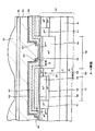
次に、図1の撮像領域4の、A―A線上における拡大断面図を図2に示す。
撮像領域4では、第1導電型、例えばN型のシリコン半導体基板10内に、第2導電型、例えばP型の第1の半導体ウェル領域11が形成され、シリコン半導体基板10の表面側には、受光センサ部2を構成するN+の半導体領域(所謂電荷蓄積領域)12とその上の表面のP++の半導体領域(正電荷蓄積領域)13からなるフォトダイオードが形成される。受光センサ部12列の一方の側には、垂直転送レジスタ3を構成するN+の転送チャネル領域15が形成され、N+の転送チャネル領域15の下には、P+の第2の半導体ウェル領域16が形成されている。受光センサ部12列の他方の側には、水平方向に隣り合う画素間を分離するための画素分離領域、即ち、高濃度のP型のチャネルストップ領域17が形成されている。受光センサ部12と垂直転送レジスタ13との間のN型の半導体基板10には、受光センサ部12に蓄積された信号電荷を、垂直転送レジスタ13に読み出すための、読み出しゲート部18が形成されている。
尚、P型の第1の半導体ウェル領域11は、例えばN型のシリコン基板10の所定の領域に、後からP型の不純物が注入されることで形成される。
Next, FIG. 2 shows an enlarged cross-sectional view of the imaging region 4 in FIG. 1 on the line AA.
In the imaging region 4, a first
The P-type first
半導体基板10の表面上には、絶縁膜19が形成され、読み出しゲート部18、N+の転送チャネル領域15及びチャネルストップ領域17上に、例えば多結晶シリコン層よりなる転送電極20が形成されている。尚、転送電極20は、3層構造で形成されている。
そして、N+の転送チャネル領域15、転送電極20とにより垂直転送レジスタ3が構成される。この転送電極20上には層間絶縁膜21を介して例えばAlからなる遮光膜22が形成される。
遮光膜22には、前述したように、例えば遮光膜22の端から入射する光によって、垂直転送レジスタ3にスミアが発生することを防止するために、張り出し部221が設けられている。
An insulating
The N +
As described above, the
遮光膜22上には、全面を覆ってプラズマSiN膜23が形成され、プラズマSiN膜23上には、全面を覆って平坦化膜24が形成され、この平坦化膜24上には、カラーフィルタ25が形成される。そして、このカラーフィルタ25上の受光センサ部2と対応する位置には、オンチップレンズ26が形成されている。
A
そして、本実施の形態の固体撮像素子1では、特に、遮光膜22が読み出しゲート部18の上方に形成され、受光センサ部2に蓄積された信号電荷を垂直転送レジスタ3へ読み出す際の読み出し電極を兼ねるように構成されている。
即ち、従来の固体撮像素子では、読み出しゲート部では、基板上にゲート絶縁膜を介して、転送電極が形成された構成であるが(図7参照)、本実施の形態の固体撮像素子1では、読み出しゲート部18では、基板上にゲート絶縁膜19を介して、遮光膜22の張り出し部221が形成された構成であり、遮光膜22が読み出し電極を兼ねる構成となっている。この遮光膜22には、読み出し電圧を印加するための配線27が接続されている。
In the solid-state imaging device 1 according to the present embodiment, in particular, the
That is, in the conventional solid-state imaging device, the readout gate portion has a configuration in which the transfer electrode is formed on the substrate via the gate insulating film (see FIG. 7), but in the solid-state imaging device 1 of the present embodiment, The
そして、さらに、本実施の形態の固体撮像素子1では、信号電荷の読み出し時以外は、遮光膜22に、読み出しゲート部に反転層(障壁)が形成されるような電圧が印加され、信号電荷の読み出し時は、遮光膜22に、反転層が消去されるような電圧が印加される。
Further, in the solid-state imaging device 1 of the present embodiment, a voltage that causes an inversion layer (barrier) to be formed in the readout gate portion is applied to the
以下、本実施の形態の固体撮像素子1における、読み出し動作を、図2〜図5を用いて具体的に説明する。
尚、図2及び図3は信号電荷の読み出し時以外を、図4及び図5は信号電荷の読み出し時を示している。
Hereinafter, the reading operation in the solid-state imaging device 1 of the present embodiment will be specifically described with reference to FIGS.
FIGS. 2 and 3 show the signal charges other than when reading, and FIGS. 4 and 5 show the signal charges when read.
先ず、信号電荷の読み出し時以外では、図2に示すように、配線27を介して、遮光膜22に、反転層が形成されるような電圧φVが印加される。ここで、本実施の形態の固体撮像素子1では、読み出しゲート部18がN型の不純物より形成されているので、反転層が形成されるような電圧φVとしては、負電圧が印加される。
First, at a time other than reading signal charges, a voltage φV that forms an inversion layer is applied to the
この際、読み出しゲート部18では、図3Aに示すように、負の電荷を持つ電子が半導体基板10の界面から半導体基板10の底部へと遠ざけられることにより、半導体基板10の界面近傍が正孔のみとなり、空乏化領域29が形成される。そして、さらに、伝導型が反転して、正の電荷をもつ正孔が読み出しゲート部18の表面部に誘起される。このようにして、図2及び図3Bに示すような反転層28が形成される。
At this time, in the read
一方、信号電荷の読み出し時では、図4に示すように、配線27を介して、遮光膜22に、上記反転層28が消去されるような読み出し電圧φVRが印加される。ここで、本実施の形態の固体撮像素子1では、反転層28は、負電圧φVが印加されることで形成されるので、反転層28が消去されるような読み出し電圧φVRとしては、正電圧が印加される。
尚、この正電圧としては、0V以上の電圧であれば、反転層28を消去することが可能である。これにより、高い読み出し電圧を印加する必要がなくなる。
On the other hand, at the time of reading the signal charge, as shown in FIG. 4, a read voltage φVR that erases the
Note that the
この際、読み出しゲート部18では、図5Aに示すように、正孔が半導体基板10の界面から半導体基板10の底部へと遠ざけられることにより、半導体基板10の界面近傍が負の電荷を持つ電子のみとなる。これにより、上述した空乏化領域29が消滅されて、図4及び図5Bに示すように、読み出しゲート部18の表面部から反転層28が消去された状態となる。
At this time, in the read
このように、本実施の形態の固体撮像素子1によれば、遮光膜22が、読み出し電極を兼ねる構成として、読み出し時以外では、この遮光膜22に読み出しゲート部18に反転層28が形成されるような電圧φV(負電圧)が印加されることで、読み出しゲート部18の表面部に反転層28が形成され、読み出し時では、遮光膜22に上記反転層28が消去されるような電圧φVR(正電圧)が印加されることで、読み出しゲート部18の表面部からは反転層28が消去されるようにしたので、信号電荷の読み出し時以外では、反転層28により、受光センサ部2から垂直転送レジスタ3への信号電荷の流出を抑えることができ、信号電荷の読み出し時では、遮光膜22に印加される読み出し電圧φVRが高くなることを抑えることができる。
As described above, according to the solid-state imaging device 1 of the present embodiment, the
また、本実施の形態の固体撮像素子1によれば、読み出しゲート部18では、基板10上に絶縁膜19を介して、遮光膜22の張り出し部221が設けられ、遮光膜22が読み出し電極を兼ねるように構成されているので、従来のように、遮光膜の張り出し部が受光センサ部上に跨るように形成されている構成に比べて、受光センサ部上に遮光膜の張り出し部がない分、開口面積が大きく、感度の高い構成にすることができる。
これにより、従来のように、受光センサ部22上の遮光膜221の張り出し部を短くしなくとも、スミア特性に影響を与えることなく、微細化することができる。
Further, according to the solid-state imaging device 1 of the present embodiment, the
As a result, it is possible to reduce the size without affecting the smear characteristics without shortening the protruding portion of the
上述した実施の形態の固体撮像素子1では、読み出しゲート部18が、N型の不純物より形成された場合において、読み出し時以外では、配線27を介して遮光膜22に負電圧が印加されることで読み出しゲート部18の表面に反転層28が形成され、読み出し時では、遮光膜22に正電圧が印加されることで反転層28が消去される構成を示したが、例えば、読み出しゲート部18が、P型の不純物より形成された場合は、読み出し時以外と読み出し時に遮光膜22に印加される電圧の極性が逆になる。
In the solid-state imaging device 1 according to the above-described embodiment, when the
即ち、このような構成の固体撮像素子の場合、読み出しゲート部18がP型の不純物より形成されているので、読み出し時以外では、反転層が形成されるような電圧φVとしては、正電圧が印加される。
一方、読み出し時では、反転層28は、正電圧が印加されることで形成されているので、反転層28が消去されるような読み出し電圧φVRとしては、負電圧が印加される。
That is, in the case of the solid-state imaging device having such a configuration, since the
On the other hand, at the time of reading, since the
このような構成とされた固体撮像素子においても、上述した実施の形態の場合と同様に、読み出し時以外では、反転層28により、受光センサ部2から垂直転送レジスタ3への信号電荷の流出を抑えることができ、読み出し時では、遮光膜22に印加される読み出し電圧φVRが高くなることを抑えることができる。
また、上述した実施の形態の場合と同様に、読み出しゲート部18では、基板10上に絶縁膜19を介して、遮光膜22の張り出し部221が設けられ、遮光膜22が読み出し電極を兼ねるように構成されているので、開口面積が広く感度の高い構成となる。これにより、受光センサ部2上の遮光膜22の張り出し部221を短くしなくとも、スミア特性に影響を与えることなく微細化することができる。
Also in the solid-state imaging device having such a configuration, as in the case of the above-described embodiment, the signal charge flows from the light receiving
Further, as in the case of the above-described embodiment, in the read
尚、本実施の形態の固体撮像素子1においては、遮光膜22が、撮像領域4において、受光センサ部2を除く領域を覆っているので、例えば、信号電荷の読み出し時に、遮光膜22に配線27を介して読み出し電圧が印加された場合、全ての受光センサ部2に蓄積された信号電荷が読み出されることになる。即ち、本実施の形態の固体撮像素子1では、全画素読み出しで信号電荷の読み出し動作が行われる。
In the solid-state imaging device 1 of the present embodiment, since the
しかしながら、例えば、遮光膜22の形状を変形させることで、本実施の形態の固体撮像素子1においても、フィールド読み出しやフレーム読み出しにより、信号電荷の読み出し動作を行うことができる。
However, for example, by changing the shape of the light-shielding
このような場合は、先ず、本実施の形態の固体撮像素子1において、例えば遮光膜22が受光センサ部2の各行毎で分断されるような構成として、読み出し電圧が受光センサ部の各行毎に印加される構成とする。そして、このような構成の固体撮像素子1において、転送電極の構成を変化させたり、読み出し電圧を印加するタイミングを、奇数行、偶数行でそれぞれ変化させたりすることで行うことができる。
尚、受光センサ部の各行毎に分断された遮光膜22は、例えば、遮光膜22の形成工程において、マスクパターンの形状を、受光センサ部の各行毎で分断された形状とすることで形成することができる。
In such a case, first, in the solid-state imaging device 1 of the present embodiment, for example, the
The
上述した実施の形態では、本発明を、IT型の固体撮像素子に適用して説明したが、IT型の固体撮像素子に限られず、例えばフレームインターライントランスファ(FIT)型の固体撮像素子にも適用することができる。 In the above-described embodiments, the present invention is applied to the IT solid-state image sensor. However, the present invention is not limited to the IT solid-state image sensor. For example, the present invention is applied to a frame interline transfer (FIT) solid-state image sensor. Can be applied.
尚、本発明は、上述の実施の形態に限定されるものではなく、本発明の要旨を逸脱しない範囲でその他様々な構成が取り得る。 The present invention is not limited to the above-described embodiment, and various other configurations can be taken without departing from the gist of the present invention.
1・・・固体撮像素子、2・・・受光センサ部、3・・・垂直転送レジスタ、4・・・撮像領域、5・・・水平転送レジスタ部、6・・・出力部、7・・・、8・・・、10・・・N型のシリコン半導体基板、11・・・P型の第1の半導体ウェル領域、12・・・N+の半導体領域、13・・・P++の読み出しゲート部、15・・・N+の転送チャネル領域、16・・・P+の第2の半導体ウェル領域、17・・・P+のチャネルストップ領域、18・・・読み出しゲート部、19・・・絶縁膜、20・・・転送電極、21・・・層間絶縁膜、22・・・遮光膜、221・・・張り出し部、23・・・プラズマSiN膜、24・・・平坦化膜、25・・・カラーフィルタ、26・・・オンチップレンズ、27・・・配線、28・・・反転層 DESCRIPTION OF SYMBOLS 1 ... Solid-state image sensor, 2 ... Light-receiving sensor part, 3 ... Vertical transfer register, 4 ... Imaging area, 5 ... Horizontal transfer register part, 6 ... Output part, 7 ... 8 ... 10 ... N-type silicon semiconductor substrate, 11 ... P-type first semiconductor well region, 12 ... N + semiconductor region, 13 ... P ++ readout Gate portion, 15... N + transfer channel region, 16... P + second semiconductor well region, 17... P + channel stop region, 18. Insulating film, 20 ... transfer electrode, 21 ... interlayer insulating film, 22 ... light shielding film, 221 ... overhang, 23 ... plasma SiN film, 24 ... flattening film, 25 ... Color filters, 26 ... On-chip lenses, 27 ... Wiring, 28 ... Rolling layer
Claims (3)
前記撮像領域において、前記受光センサ部を除く領域が遮光膜で覆われ、
前記遮光膜が、前記受光センサ部に蓄積された信号電荷を、前記垂直転送レジスタに読み出すための読み出し電極を兼ね、
前記信号電荷の読み出し時以外は、前記遮光膜に、前記読み出しゲート部の表面に反転層が形成されるような電圧が印加され、
前記信号電荷の読み出し時は、前記遮光膜に、前記反転層が消去されるような電圧が印加される
ことを特徴とする固体撮像素子。 A light receiving sensor unit and a vertical transfer register are formed, and a reading gate unit is formed between the light receiving sensor unit and the vertical transfer register to form an imaging region,
In the imaging region, the region excluding the light receiving sensor portion is covered with a light shielding film,
The light shielding film also serves as a readout electrode for reading the signal charge accumulated in the light receiving sensor unit to the vertical transfer register,
Except at the time of reading out the signal charge, a voltage is applied to the light shielding film so that an inversion layer is formed on the surface of the readout gate portion.
At the time of reading out the signal charge, a voltage that erases the inversion layer is applied to the light shielding film.
The read gate portion is formed of a P-type semiconductor region, and a positive voltage is applied to the light shielding film so that an inversion layer is formed on the surface of the read gate portion except when the signal charge is read. The solid-state imaging device according to claim 1, wherein a negative voltage is applied so that the inversion layer is erased when reading out the electric charge.
Priority Applications (1)
| Application Number | Priority Date | Filing Date | Title |
|---|---|---|---|
| JP2003338169A JP2005109021A (en) | 2003-09-29 | 2003-09-29 | Solid state imaging device |
Applications Claiming Priority (1)
| Application Number | Priority Date | Filing Date | Title |
|---|---|---|---|
| JP2003338169A JP2005109021A (en) | 2003-09-29 | 2003-09-29 | Solid state imaging device |
Publications (2)
| Publication Number | Publication Date |
|---|---|
| JP2005109021A true JP2005109021A (en) | 2005-04-21 |
| JP2005109021A5 JP2005109021A5 (en) | 2006-06-22 |
Family
ID=34533763
Family Applications (1)
| Application Number | Title | Priority Date | Filing Date |
|---|---|---|---|
| JP2003338169A Pending JP2005109021A (en) | 2003-09-29 | 2003-09-29 | Solid state imaging device |
Country Status (1)
| Country | Link |
|---|---|
| JP (1) | JP2005109021A (en) |
Cited By (8)
| Publication number | Priority date | Publication date | Assignee | Title |
|---|---|---|---|---|
| US7714404B2 (en) | 2007-09-06 | 2010-05-11 | Fujifilm Corporation | Solid-state imaging device |
| US7772616B2 (en) | 2007-09-11 | 2010-08-10 | Fujifilm Corporation | Solid-state imaging device and imaging apparatus |
| CN102034844A (en) * | 2009-09-28 | 2011-04-27 | 索尼公司 | Solid-state image pickup device, method for manufacturing the same, and electronic apparatus |
| JP2011129723A (en) * | 2009-12-17 | 2011-06-30 | Sharp Corp | Method of manufacturing solid-state imaging device |
| US7994461B2 (en) | 2008-07-01 | 2011-08-09 | Fujifilm Corporation | Solid-state imaging device and imaging apparatus |
| US8085331B2 (en) | 2007-12-21 | 2011-12-27 | Panasonic Corporation | Solid-state imaging device, driving method thereof, and camera |
| CN102800685A (en) * | 2011-05-27 | 2012-11-28 | 佳能株式会社 | Solid-state image pickup apparatus and image pickup system |
| US8593554B2 (en) | 2008-10-17 | 2013-11-26 | Sony Corporation | Solid-state imaging apparatus, camera, and method of manufacturing solid-state imaging apparatus |
Citations (3)
| Publication number | Priority date | Publication date | Assignee | Title |
|---|---|---|---|---|
| JPH04245679A (en) * | 1991-01-31 | 1992-09-02 | Toshiba Corp | Solid-state imaging device |
| JP2002289534A (en) * | 2001-03-26 | 2002-10-04 | Sony Corp | Method for fabricating semiconductor device and method for sorting solid-state imaging device |
| JP2003234463A (en) * | 2002-02-08 | 2003-08-22 | Sony Corp | Charge coupled device |
-
2003
- 2003-09-29 JP JP2003338169A patent/JP2005109021A/en active Pending
Patent Citations (3)
| Publication number | Priority date | Publication date | Assignee | Title |
|---|---|---|---|---|
| JPH04245679A (en) * | 1991-01-31 | 1992-09-02 | Toshiba Corp | Solid-state imaging device |
| JP2002289534A (en) * | 2001-03-26 | 2002-10-04 | Sony Corp | Method for fabricating semiconductor device and method for sorting solid-state imaging device |
| JP2003234463A (en) * | 2002-02-08 | 2003-08-22 | Sony Corp | Charge coupled device |
Cited By (12)
| Publication number | Priority date | Publication date | Assignee | Title |
|---|---|---|---|---|
| US7714404B2 (en) | 2007-09-06 | 2010-05-11 | Fujifilm Corporation | Solid-state imaging device |
| US7772616B2 (en) | 2007-09-11 | 2010-08-10 | Fujifilm Corporation | Solid-state imaging device and imaging apparatus |
| US8085331B2 (en) | 2007-12-21 | 2011-12-27 | Panasonic Corporation | Solid-state imaging device, driving method thereof, and camera |
| US7994461B2 (en) | 2008-07-01 | 2011-08-09 | Fujifilm Corporation | Solid-state imaging device and imaging apparatus |
| US8593554B2 (en) | 2008-10-17 | 2013-11-26 | Sony Corporation | Solid-state imaging apparatus, camera, and method of manufacturing solid-state imaging apparatus |
| CN102034844A (en) * | 2009-09-28 | 2011-04-27 | 索尼公司 | Solid-state image pickup device, method for manufacturing the same, and electronic apparatus |
| JP2011129723A (en) * | 2009-12-17 | 2011-06-30 | Sharp Corp | Method of manufacturing solid-state imaging device |
| CN102800685A (en) * | 2011-05-27 | 2012-11-28 | 佳能株式会社 | Solid-state image pickup apparatus and image pickup system |
| US9224774B2 (en) | 2011-05-27 | 2015-12-29 | Canon Kabushiki Kaisha | Solid-state image pickup apparatus, and image pickup system using solid-state image pickup apparatus |
| US9553117B2 (en) | 2011-05-27 | 2017-01-24 | Canon Kabushiki Kaisha | Solid-state image pickup apparatus, and image pickup system using solid-state image pickup apparatus |
| US9893104B2 (en) | 2011-05-27 | 2018-02-13 | Canon Kabushiki Kaisha | Solid-state image pickup apparatus, and image pickup system using solid-state image pickup apparatus |
| US10418398B2 (en) | 2011-05-27 | 2019-09-17 | Canon Kabushiki Kaisha | Solid-state image pickup apparatus, and image pickup system using solid-state image pickup apparatus having metal film with first and second portions |
Similar Documents
| Publication | Publication Date | Title |
|---|---|---|
| TWI479647B (en) | A solid-state imaging device, a manufacturing method of a solid-state imaging device, and an electronic device | |
| JP4621719B2 (en) | Back-illuminated image sensor | |
| JP5537523B2 (en) | Solid-state imaging device | |
| JP4224036B2 (en) | Image sensor with embedded photodiode region and method of manufacturing the same | |
| KR101159032B1 (en) | Solid-state imaging device | |
| JP2006245499A (en) | Solid state imaging apparatus | |
| JP4371145B2 (en) | Solid-state imaging device and imaging device | |
| US20100214464A1 (en) | Solid-state imaging apparatus | |
| JP2007115787A (en) | Solid-state imaging element | |
| JP2005109021A (en) | Solid state imaging device | |
| JP2005217302A (en) | Solid-state imaging device | |
| JP2005268644A (en) | Back irradiation type solid-state image pickup element, electronic equipment module, and camera module | |
| JP2011054596A (en) | Ccd image sensor | |
| JP2001057421A (en) | Solid state image sensor | |
| JP4784655B2 (en) | Solid-state imaging device and electronic apparatus | |
| JP2007035950A (en) | Solid-state image pickup device, manufacturing method thereof and camera | |
| JP2008193050A (en) | Solid-state imaging apparatus and imaging apparatus | |
| JP4867309B2 (en) | Solid-state imaging device, manufacturing method thereof, and camera | |
| JP2013145933A (en) | Solid state imaging element, solid state imaging device and electronic apparatus | |
| JP2006319184A (en) | Solid-state imaging device and camera | |
| JP2003347537A (en) | Solid-state image pickup element | |
| JP2007184467A (en) | Solid-state imaging element | |
| JP2005093915A (en) | Solid state imaging device | |
| JP2009272338A (en) | Solid-state image sensor and imaging device | |
| JP5002941B2 (en) | Solid-state imaging device, manufacturing method thereof, and camera |
Legal Events
| Date | Code | Title | Description |
|---|---|---|---|
| A521 | Request for written amendment filed |
Free format text: JAPANESE INTERMEDIATE CODE: A523 Effective date: 20060508 |
|
| A621 | Written request for application examination |
Free format text: JAPANESE INTERMEDIATE CODE: A621 Effective date: 20060508 |
|
| A977 | Report on retrieval |
Free format text: JAPANESE INTERMEDIATE CODE: A971007 Effective date: 20090601 |
|
| A131 | Notification of reasons for refusal |
Free format text: JAPANESE INTERMEDIATE CODE: A131 Effective date: 20090609 |
|
| A521 | Request for written amendment filed |
Free format text: JAPANESE INTERMEDIATE CODE: A523 Effective date: 20090727 |
|
| A131 | Notification of reasons for refusal |
Free format text: JAPANESE INTERMEDIATE CODE: A131 Effective date: 20091020 |
|
| A521 | Request for written amendment filed |
Free format text: JAPANESE INTERMEDIATE CODE: A523 Effective date: 20091214 |
|
| A02 | Decision of refusal |
Free format text: JAPANESE INTERMEDIATE CODE: A02 Effective date: 20100330 |