JP6091550B2 - 撮像素子及び撮像装置 - Google Patents
撮像素子及び撮像装置 Download PDFInfo
- Publication number
- JP6091550B2 JP6091550B2 JP2015115593A JP2015115593A JP6091550B2 JP 6091550 B2 JP6091550 B2 JP 6091550B2 JP 2015115593 A JP2015115593 A JP 2015115593A JP 2015115593 A JP2015115593 A JP 2015115593A JP 6091550 B2 JP6091550 B2 JP 6091550B2
- Authority
- JP
- Japan
- Prior art keywords
- column
- region
- circuit
- semiconductor substrate
- pixel
- Prior art date
- Legal status (The legal status is an assumption and is not a legal conclusion. Google has not performed a legal analysis and makes no representation as to the accuracy of the status listed.)
- Active
Links
Images


Landscapes
- Solid State Image Pick-Up Elements (AREA)
- Transforming Light Signals Into Electric Signals (AREA)
Description
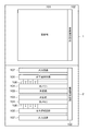
2 領域
101 画素部
102 垂直選択回路
103 列回路
104 列メモリ
105 水平選択回路
106 出力信号線
107 出力回路
Claims (10)
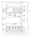
- 互いに積層された第1の半導体基板および第2の半導体基板と、
複数の画素が行列状に配列された画素部と、
前記画素部の複数の画素から列毎に信号が出力される複数の列信号線と、
各々が少なくともAD変換器を備え、前記列信号線に出力された信号に所定の処理を施すために列毎に設けられた複数の列回路と、
前記複数の列回路で所定の処理を施された信号を保持するために列毎に設けられた複数の列メモリと、を有する撮像素子において、
前記撮像素子を光入射面側から見た場合に、前記複数の列回路および前記複数の列メモリが前記画素部の下に重なる位置になるように、前記画素部が前記第1の半導体基板の領域に形成されるとともに前記複数の列回路および前記複数の列メモリが前記第2の半導体基板の領域に形成され、
前記第2の半導体基板の領域に形成された前記複数の列回路および前記複数の列メモリが、行に沿う方向または列に沿う方向の少なくとも一方において、少なくとも隣接する2列で異なる位置に配置されていることを特徴とする撮像素子。 - 前記第2の半導体基板の領域に形成された前記複数の列回路および前記複数の列メモリが、行に沿う方向および列に沿う方向において、少なくとも隣接する2列で異なる位置に配置されていることを特徴とする請求項1に記載の撮像素子。
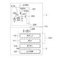
- 前記第1の半導体基板の領域と前記第2の半導体基板の領域を電気的に接続する列毎の接続ポイントが、列に沿う方向において、少なくとも隣接する2列で異なる位置に設けられることを特徴とする請求項1又は2に記載の撮像素子。
- 前記列毎の接続ポイントがそれぞれ前記複数の列信号線にあることを特徴とする請求項3記載の撮像素子。
- 前記第2の半導体基板の領域に所定の画像処理を施すデジタル回路が配置されていることを特徴とする請求項1乃至4のいずれか1項に記載の撮像素子。
- 前記画素部を駆動する駆動回路をさらに備え、
前記駆動回路の少なくとも一部が前記第1の半導体基板の領域及び前記第2の半導体基板の領域に別々に形成されていることを特徴とする請求項1乃至5のいずれか1項に記載の撮像素子。 - 前記駆動回路の少なくとも一部が前記第1の半導体基板の領域に形成されていることを特徴とする請求項6記載の撮像素子。
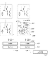
- 前記画素部の前記複数の画素の各々は、光電変換により電荷を発生する光電変換素子と、前記光電変換素子で発生した電荷を一時的に蓄えるフローティングディフュージョン部と、前記フローティングディフュージョン部の電位に応じた信号を出力する増幅部とを有することを特徴とする請求項1乃至7のいずれか1項に記載の撮像素子。
- 前記画素部の各々は、さらに、前記光電変換素子から前記フローティングディフュージョン部に電荷を転送する転送部と、前記フローティングディフュージョン部に接続され前記フローティングディフュージョン部をリセットするリセット部とを備えることを特徴とする請求項8記載の撮像素子。
- 請求項1乃至9の何れか1項に記載の撮像素子を備えることを特徴とする撮像装置。
Priority Applications (1)
| Application Number | Priority Date | Filing Date | Title |
|---|---|---|---|
| JP2015115593A JP6091550B2 (ja) | 2011-08-02 | 2015-06-08 | 撮像素子及び撮像装置 |
Applications Claiming Priority (3)
| Application Number | Priority Date | Filing Date | Title |
|---|---|---|---|
| JP2011169291 | 2011-08-02 | ||
| JP2011169291 | 2011-08-02 | ||
| JP2015115593A JP6091550B2 (ja) | 2011-08-02 | 2015-06-08 | 撮像素子及び撮像装置 |
Related Parent Applications (1)
| Application Number | Title | Priority Date | Filing Date |
|---|---|---|---|
| JP2012159605A Division JP5791571B2 (ja) | 2011-08-02 | 2012-07-18 | 撮像素子及び撮像装置 |
Related Child Applications (1)
| Application Number | Title | Priority Date | Filing Date |
|---|---|---|---|
| JP2017021967A Division JP6355773B2 (ja) | 2011-08-02 | 2017-02-09 | 撮像素子及び撮像装置 |
Publications (2)
| Publication Number | Publication Date |
|---|---|
| JP2015213327A JP2015213327A (ja) | 2015-11-26 |
| JP6091550B2 true JP6091550B2 (ja) | 2017-03-08 |
Family
ID=54697333
Family Applications (6)
| Application Number | Title | Priority Date | Filing Date |
|---|---|---|---|
| JP2015115593A Active JP6091550B2 (ja) | 2011-08-02 | 2015-06-08 | 撮像素子及び撮像装置 |
| JP2017021967A Expired - Fee Related JP6355773B2 (ja) | 2011-08-02 | 2017-02-09 | 撮像素子及び撮像装置 |
| JP2018041821A Active JP6666047B2 (ja) | 2011-08-02 | 2018-03-08 | 撮像素子及び撮像装置 |
| JP2020023422A Active JP6907358B2 (ja) | 2011-08-02 | 2020-02-14 | 撮像素子及び撮像装置 |
| JP2021107806A Active JP7135167B2 (ja) | 2011-08-02 | 2021-06-29 | 撮像素子及び撮像装置 |
| JP2022137140A Active JP7497396B2 (ja) | 2011-08-02 | 2022-08-30 | 撮像素子及び撮像装置 |
Family Applications After (5)
| Application Number | Title | Priority Date | Filing Date |
|---|---|---|---|
| JP2017021967A Expired - Fee Related JP6355773B2 (ja) | 2011-08-02 | 2017-02-09 | 撮像素子及び撮像装置 |
| JP2018041821A Active JP6666047B2 (ja) | 2011-08-02 | 2018-03-08 | 撮像素子及び撮像装置 |
| JP2020023422A Active JP6907358B2 (ja) | 2011-08-02 | 2020-02-14 | 撮像素子及び撮像装置 |
| JP2021107806A Active JP7135167B2 (ja) | 2011-08-02 | 2021-06-29 | 撮像素子及び撮像装置 |
| JP2022137140A Active JP7497396B2 (ja) | 2011-08-02 | 2022-08-30 | 撮像素子及び撮像装置 |
Country Status (1)
| Country | Link |
|---|---|
| JP (6) | JP6091550B2 (ja) |
Families Citing this family (6)
| Publication number | Priority date | Publication date | Assignee | Title |
|---|---|---|---|---|
| JP6856983B2 (ja) * | 2016-06-30 | 2021-04-14 | キヤノン株式会社 | 光電変換装置及びカメラ |
| JP7278209B2 (ja) * | 2017-04-25 | 2023-05-19 | ヌヴォトンテクノロジージャパン株式会社 | 固体撮像装置および撮像装置 |
| JP7102119B2 (ja) | 2017-09-29 | 2022-07-19 | キヤノン株式会社 | 半導体装置および機器 |
| US20230299109A1 (en) * | 2022-03-18 | 2023-09-21 | Taiwan Semiconductor Manufacturing Company, Ltd. | Stacked image sensors and methods of manufacturing thereof |
| US12225304B2 (en) * | 2022-04-27 | 2025-02-11 | Semiconductor Components Industries, Llc | Expanded image sensor pixel array |
| JP2025133575A (ja) | 2024-03-01 | 2025-09-11 | ソニーセミコンダクタソリューションズ株式会社 | 光検出装置および電子機器 |
Family Cites Families (14)
| Publication number | Priority date | Publication date | Assignee | Title |
|---|---|---|---|---|
| US6466265B1 (en) | 1998-06-22 | 2002-10-15 | Eastman Kodak Company | Parallel output architectures for CMOS active pixel sensors |
| JP2000324397A (ja) * | 1999-05-12 | 2000-11-24 | Sony Corp | 固体撮像素子 |
| JP4349232B2 (ja) * | 2004-07-30 | 2009-10-21 | ソニー株式会社 | 半導体モジュール及びmos型固体撮像装置 |
| US8144227B2 (en) * | 2004-09-02 | 2012-03-27 | Sony Corporation | Image pickup device and image pickup result outputting method |
| JP4687139B2 (ja) * | 2005-02-23 | 2011-05-25 | ソニー株式会社 | 固体撮像装置、固体撮像装置の駆動方法および撮像装置 |
| TW201101476A (en) * | 2005-06-02 | 2011-01-01 | Sony Corp | Semiconductor image sensor module and method of manufacturing the same |
| JP4289377B2 (ja) * | 2006-08-21 | 2009-07-01 | ソニー株式会社 | 物理量検出装置及び撮像装置 |
| JP2008235478A (ja) | 2007-03-19 | 2008-10-02 | Nikon Corp | 撮像素子 |
| JP4941490B2 (ja) * | 2009-03-24 | 2012-05-30 | ソニー株式会社 | 固体撮像装置、及び電子機器 |
| JP2010283787A (ja) * | 2009-06-08 | 2010-12-16 | Panasonic Corp | 撮像装置 |
| JP5521721B2 (ja) | 2009-08-28 | 2014-06-18 | ソニー株式会社 | 撮像素子およびカメラシステム |
| TWI515885B (zh) | 2009-12-25 | 2016-01-01 | 新力股份有限公司 | 半導體元件及其製造方法,及電子裝置 |
| JP5685898B2 (ja) * | 2010-01-08 | 2015-03-18 | ソニー株式会社 | 半導体装置、固体撮像装置、およびカメラシステム |
| JP5633323B2 (ja) * | 2010-11-11 | 2014-12-03 | ソニー株式会社 | 固体撮像装置及び電子機器 |
-
2015
- 2015-06-08 JP JP2015115593A patent/JP6091550B2/ja active Active
-
2017
- 2017-02-09 JP JP2017021967A patent/JP6355773B2/ja not_active Expired - Fee Related
-
2018
- 2018-03-08 JP JP2018041821A patent/JP6666047B2/ja active Active
-
2020
- 2020-02-14 JP JP2020023422A patent/JP6907358B2/ja active Active
-
2021
- 2021-06-29 JP JP2021107806A patent/JP7135167B2/ja active Active
-
2022
- 2022-08-30 JP JP2022137140A patent/JP7497396B2/ja active Active
Also Published As
| Publication number | Publication date |
|---|---|
| JP2022171700A (ja) | 2022-11-11 |
| JP7497396B2 (ja) | 2024-06-10 |
| JP6666047B2 (ja) | 2020-03-13 |
| JP2018102002A (ja) | 2018-06-28 |
| JP6355773B2 (ja) | 2018-07-11 |
| JP7135167B2 (ja) | 2022-09-12 |
| JP6907358B2 (ja) | 2021-07-21 |
| JP2017092990A (ja) | 2017-05-25 |
| JP2015213327A (ja) | 2015-11-26 |
| JP2021166395A (ja) | 2021-10-14 |
| JP2020108152A (ja) | 2020-07-09 |
Similar Documents
| Publication | Publication Date | Title |
|---|---|---|
| JP5791571B2 (ja) | 撮像素子及び撮像装置 | |
| JP7135167B2 (ja) | 撮像素子及び撮像装置 | |
| JP5633323B2 (ja) | 固体撮像装置及び電子機器 | |
| JP4941490B2 (ja) | 固体撮像装置、及び電子機器 | |
| CN101510552B (zh) | 固态成像装置、照相机和电子装置 | |
| JP2015012303A (ja) | 固体撮像装置および電子機器 | |
| JP4985862B2 (ja) | 固体撮像装置の駆動方法 | |
| JP5072466B2 (ja) | 撮像装置 |
Legal Events
| Date | Code | Title | Description |
|---|---|---|---|
| A977 | Report on retrieval |
Free format text: JAPANESE INTERMEDIATE CODE: A971007 Effective date: 20160620 |
|
| A131 | Notification of reasons for refusal |
Free format text: JAPANESE INTERMEDIATE CODE: A131 Effective date: 20160712 |
|
| A521 | Request for written amendment filed |
Free format text: JAPANESE INTERMEDIATE CODE: A523 Effective date: 20160912 |
|
| TRDD | Decision of grant or rejection written | ||
| A01 | Written decision to grant a patent or to grant a registration (utility model) |
Free format text: JAPANESE INTERMEDIATE CODE: A01 Effective date: 20170110 |
|
| A61 | First payment of annual fees (during grant procedure) |
Free format text: JAPANESE INTERMEDIATE CODE: A61 Effective date: 20170207 |
|
| R151 | Written notification of patent or utility model registration |
Ref document number: 6091550 Country of ref document: JP Free format text: JAPANESE INTERMEDIATE CODE: R151 |