JP6073383B2 - Small rotatable sputter device for sputter deposition - Google Patents
Small rotatable sputter device for sputter deposition Download PDFInfo
- Publication number
- JP6073383B2 JP6073383B2 JP2014561293A JP2014561293A JP6073383B2 JP 6073383 B2 JP6073383 B2 JP 6073383B2 JP 2014561293 A JP2014561293 A JP 2014561293A JP 2014561293 A JP2014561293 A JP 2014561293A JP 6073383 B2 JP6073383 B2 JP 6073383B2
- Authority
- JP
- Japan
- Prior art keywords
- sputter device
- sputter
- rotatable
- coating
- deposition
- Prior art date
- Legal status (The legal status is an assumption and is not a legal conclusion. Google has not performed a legal analysis and makes no representation as to the accuracy of the status listed.)
- Expired - Fee Related
Links
- 238000004544 sputter deposition Methods 0.000 title claims description 11
- 238000000151 deposition Methods 0.000 claims description 133
- 230000008021 deposition Effects 0.000 claims description 118
- 238000000576 coating method Methods 0.000 claims description 89
- 239000011248 coating agent Substances 0.000 claims description 85
- 239000000463 material Substances 0.000 claims description 81
- 238000000034 method Methods 0.000 claims description 49
- 229910052581 Si3N4 Inorganic materials 0.000 claims description 3
- VYPSYNLAJGMNEJ-UHFFFAOYSA-N Silicium dioxide Chemical compound O=[Si]=O VYPSYNLAJGMNEJ-UHFFFAOYSA-N 0.000 claims description 3
- GWEVSGVZZGPLCZ-UHFFFAOYSA-N Titan oxide Chemical compound O=[Ti]=O GWEVSGVZZGPLCZ-UHFFFAOYSA-N 0.000 claims description 3
- 239000011810 insulating material Substances 0.000 claims description 3
- TWNQGVIAIRXVLR-UHFFFAOYSA-N oxo(oxoalumanyloxy)alumane Chemical compound O=[Al]O[Al]=O TWNQGVIAIRXVLR-UHFFFAOYSA-N 0.000 claims description 3
- HQVNEWCFYHHQES-UHFFFAOYSA-N silicon nitride Chemical compound N12[Si]34N5[Si]62N3[Si]51N64 HQVNEWCFYHHQES-UHFFFAOYSA-N 0.000 claims description 3
- 229910052814 silicon oxide Inorganic materials 0.000 claims description 3
- OGIDPMRJRNCKJF-UHFFFAOYSA-N titanium oxide Inorganic materials [Ti]=O OGIDPMRJRNCKJF-UHFFFAOYSA-N 0.000 claims description 3
- 239000000758 substrate Substances 0.000 description 84
- 230000008569 process Effects 0.000 description 18
- 239000002245 particle Substances 0.000 description 9
- 239000007789 gas Substances 0.000 description 6
- 238000005137 deposition process Methods 0.000 description 5
- 238000005240 physical vapour deposition Methods 0.000 description 5
- 238000010586 diagram Methods 0.000 description 4
- 229910052710 silicon Inorganic materials 0.000 description 4
- 239000010703 silicon Substances 0.000 description 4
- 238000005546 reactive sputtering Methods 0.000 description 3
- IJGRMHOSHXDMSA-UHFFFAOYSA-N Atomic nitrogen Chemical compound N#N IJGRMHOSHXDMSA-UHFFFAOYSA-N 0.000 description 2
- 229910004298 SiO 2 Inorganic materials 0.000 description 2
- QVGXLLKOCUKJST-UHFFFAOYSA-N atomic oxygen Chemical compound [O] QVGXLLKOCUKJST-UHFFFAOYSA-N 0.000 description 2
- 238000001816 cooling Methods 0.000 description 2
- 239000001301 oxygen Substances 0.000 description 2
- 229910052760 oxygen Inorganic materials 0.000 description 2
- 239000013077 target material Substances 0.000 description 2
- XUIMIQQOPSSXEZ-UHFFFAOYSA-N Silicon Chemical compound [Si] XUIMIQQOPSSXEZ-UHFFFAOYSA-N 0.000 description 1
- RTAQQCXQSZGOHL-UHFFFAOYSA-N Titanium Chemical compound [Ti] RTAQQCXQSZGOHL-UHFFFAOYSA-N 0.000 description 1
- 229910052782 aluminium Inorganic materials 0.000 description 1
- XAGFODPZIPBFFR-UHFFFAOYSA-N aluminium Chemical compound [Al] XAGFODPZIPBFFR-UHFFFAOYSA-N 0.000 description 1
- 239000000919 ceramic Substances 0.000 description 1
- 150000001875 compounds Chemical class 0.000 description 1
- 230000001419 dependent effect Effects 0.000 description 1
- 238000009826 distribution Methods 0.000 description 1
- 230000003628 erosive effect Effects 0.000 description 1
- 239000011888 foil Substances 0.000 description 1
- 239000011521 glass Substances 0.000 description 1
- 238000010438 heat treatment Methods 0.000 description 1
- 238000004519 manufacturing process Methods 0.000 description 1
- 230000007246 mechanism Effects 0.000 description 1
- 229910052751 metal Inorganic materials 0.000 description 1
- 239000002184 metal Substances 0.000 description 1
- 238000004377 microelectronic Methods 0.000 description 1
- 238000012986 modification Methods 0.000 description 1
- 230000004048 modification Effects 0.000 description 1
- 229910052757 nitrogen Inorganic materials 0.000 description 1
- 230000008092 positive effect Effects 0.000 description 1
- 239000004065 semiconductor Substances 0.000 description 1
- 239000007790 solid phase Substances 0.000 description 1
- 239000010936 titanium Substances 0.000 description 1
- 229910052719 titanium Inorganic materials 0.000 description 1
Images


Classifications
-
- H—ELECTRICITY
- H01—ELECTRIC ELEMENTS
- H01J—ELECTRIC DISCHARGE TUBES OR DISCHARGE LAMPS
- H01J37/00—Discharge tubes with provision for introducing objects or material to be exposed to the discharge, e.g. for the purpose of examination or processing thereof
- H01J37/32—Gas-filled discharge tubes
- H01J37/34—Gas-filled discharge tubes operating with cathodic sputtering
- H01J37/3411—Constructional aspects of the reactor
- H01J37/3414—Targets
-
- C—CHEMISTRY; METALLURGY
- C23—COATING METALLIC MATERIAL; COATING MATERIAL WITH METALLIC MATERIAL; CHEMICAL SURFACE TREATMENT; DIFFUSION TREATMENT OF METALLIC MATERIAL; COATING BY VACUUM EVAPORATION, BY SPUTTERING, BY ION IMPLANTATION OR BY CHEMICAL VAPOUR DEPOSITION, IN GENERAL; INHIBITING CORROSION OF METALLIC MATERIAL OR INCRUSTATION IN GENERAL
- C23C—COATING METALLIC MATERIAL; COATING MATERIAL WITH METALLIC MATERIAL; SURFACE TREATMENT OF METALLIC MATERIAL BY DIFFUSION INTO THE SURFACE, BY CHEMICAL CONVERSION OR SUBSTITUTION; COATING BY VACUUM EVAPORATION, BY SPUTTERING, BY ION IMPLANTATION OR BY CHEMICAL VAPOUR DEPOSITION, IN GENERAL
- C23C14/00—Coating by vacuum evaporation, by sputtering or by ion implantation of the coating forming material
- C23C14/22—Coating by vacuum evaporation, by sputtering or by ion implantation of the coating forming material characterised by the process of coating
- C23C14/34—Sputtering
- C23C14/35—Sputtering by application of a magnetic field, e.g. magnetron sputtering
-
- H—ELECTRICITY
- H01—ELECTRIC ELEMENTS
- H01J—ELECTRIC DISCHARGE TUBES OR DISCHARGE LAMPS
- H01J37/00—Discharge tubes with provision for introducing objects or material to be exposed to the discharge, e.g. for the purpose of examination or processing thereof
- H01J37/32—Gas-filled discharge tubes
- H01J37/32431—Constructional details of the reactor
- H01J37/32733—Means for moving the material to be treated
- H01J37/32752—Means for moving the material to be treated for moving the material across the discharge
- H01J37/32761—Continuous moving
- H01J37/3277—Continuous moving of continuous material
-
- H—ELECTRICITY
- H01—ELECTRIC ELEMENTS
- H01J—ELECTRIC DISCHARGE TUBES OR DISCHARGE LAMPS
- H01J37/00—Discharge tubes with provision for introducing objects or material to be exposed to the discharge, e.g. for the purpose of examination or processing thereof
- H01J37/32—Gas-filled discharge tubes
- H01J37/34—Gas-filled discharge tubes operating with cathodic sputtering
- H01J37/3402—Gas-filled discharge tubes operating with cathodic sputtering using supplementary magnetic fields
- H01J37/3405—Magnetron sputtering
-
- H—ELECTRICITY
- H01—ELECTRIC ELEMENTS
- H01J—ELECTRIC DISCHARGE TUBES OR DISCHARGE LAMPS
- H01J37/00—Discharge tubes with provision for introducing objects or material to be exposed to the discharge, e.g. for the purpose of examination or processing thereof
- H01J37/32—Gas-filled discharge tubes
- H01J37/34—Gas-filled discharge tubes operating with cathodic sputtering
- H01J37/3411—Constructional aspects of the reactor
- H01J37/3414—Targets
- H01J37/3417—Arrangements
-
- H—ELECTRICITY
- H01—ELECTRIC ELEMENTS
- H01J—ELECTRIC DISCHARGE TUBES OR DISCHARGE LAMPS
- H01J37/00—Discharge tubes with provision for introducing objects or material to be exposed to the discharge, e.g. for the purpose of examination or processing thereof
- H01J37/32—Gas-filled discharge tubes
- H01J37/34—Gas-filled discharge tubes operating with cathodic sputtering
- H01J37/3411—Constructional aspects of the reactor
- H01J37/3414—Targets
- H01J37/342—Hollow targets
Description
本発明の実施形態は、堆積チャンバ内のスパッタデバイスおよび堆積プロセスで材料を堆積させる方法に関する。本発明の実施形態は、詳細には、回転可能なスパッタデバイス、特にスパッタ堆積チャンバ内の回転可能なスパッタデバイスに関する。 Embodiments of the invention relate to a sputter device in a deposition chamber and a method for depositing material with a deposition process. Embodiments of the present invention relate specifically to a rotatable sputter device, and more particularly to a rotatable sputter device in a sputter deposition chamber.
基板上に材料を堆積させるには、いくつかの方法が知られている。たとえば、スパッタプロセスなどの物理的気相堆積(PVD)プロセスによって、基板を被覆することができる。典型的には、このプロセスは、プロセス装置またはプロセスチャンバ内で実行され、被覆すべき基板はこの装置内に配置される、または装置を通るように案内される。堆積材料は、装置内に提供される。PVDプロセスが実行される場合、堆積材料は典型的には固相であり、プロセス中に反応ガスを添加することができる。基板上の堆積には複数の材料を使用することができ、とりわけセラミックを使用することができる。 Several methods are known for depositing material on a substrate. For example, the substrate can be coated by a physical vapor deposition (PVD) process such as a sputter process. Typically, the process is performed in a process apparatus or process chamber, and the substrate to be coated is placed in or guided through the apparatus. The deposition material is provided in the apparatus. When a PVD process is performed, the deposition material is typically a solid phase, and a reactive gas can be added during the process. Multiple materials can be used for deposition on the substrate, especially ceramic.
被覆された材料は、いくつかの用途およびいくつかの技術分野で使用することができる。たとえば、半導体デバイスの生成などのマイクロエレクトロニクスの分野で利用される。また、ディスプレイ向けの基板も、PVDプロセスによって被覆されることが多い。さらなる用途には、絶縁パネル、有機発光ダイオード(OLED)パネルだけでなく、ハードディスク、CD、DVDなどを含むことができる。 The coated material can be used in several applications and several technical fields. For example, it is used in the field of microelectronics such as production of semiconductor devices. Also, substrates for displays are often coated by a PVD process. Further applications can include hard disks, CDs, DVDs, etc., as well as insulating panels, organic light emitting diode (OLED) panels.
被覆プロセスを実行するために、基板は堆積チャンバ内に配置される、または堆積チャンバを通るように案内される。たとえば、被覆ドラムなどのいくつかの案内デバイスによって、堆積チャンバを通るように被覆すべきウエブを案内することができる。スパッタデバイスは、基板上に堆積させるべき材料から作られたターゲットを提供する。被覆すべき基板は、スパッタデバイスを通り過ぎて案内され、したがってターゲットから放出された材料は、スパッタデバイスを通過しながら基板に到達する。被覆ドラム上で基板を案内することは非常に空間効率がよいが、被覆ドラムのため、被覆すべき基板は短時間しかスパッタデバイスに面することがなく、その結果、ターゲットから放出された材料が被覆すべき基板上に堆積する割合が低くなる。したがって、堆積させるべき材料の大部分は、基板に到達することなく、堆積装置内で無駄になる。 To perform the coating process, the substrate is placed in or guided through the deposition chamber. For example, several guiding devices, such as a coating drum, can guide the web to be coated through the deposition chamber. A sputter device provides a target made of a material to be deposited on a substrate. The substrate to be coated is guided past the sputter device, so that the material released from the target reaches the substrate while passing through the sputter device. Guiding the substrate on the coating drum is very space efficient, but because of the coating drum, the substrate to be coated only faces the sputter device for a short time, so that the material released from the target is The rate of deposition on the substrate to be coated is low. Thus, most of the material to be deposited is wasted in the deposition apparatus without reaching the substrate.
上記を考慮して、本発明の目的は、当技術分野の問題の少なくともいくつかを克服する、堆積装置およびウエブ上に材料を堆積させる方法を提供することである。 In view of the above, it is an object of the present invention to provide a deposition apparatus and method for depositing material on a web that overcomes at least some of the problems in the art.
上記に照らして、独立請求項1に記載の堆積装置、および独立請求項12に記載の堆積材料を堆積させる方法が提供される。本発明のさらなる態様、利点、および特徴は、従属請求項、明細書、および添付の図面から明らかである。 In light of the above, a deposition apparatus according to independent claim 1 and a method for depositing a deposition material according to independent claim 12 are provided. Further aspects, advantages and features of the invention will be apparent from the dependent claims, the description and the attached drawings.
一実施形態によれば、ウエブ上に堆積材料を堆積させる堆積装置が提供される。この堆積装置は、第1の回転可能なスパッタデバイスに対する第1の軸を画定する第1のスパッタデバイス支持体と、第2の回転可能なスパッタデバイスに対する第2の軸を画定する第2のスパッタデバイス支持体と、被覆窓とを含む。第1のスパッタデバイス支持体および第2のスパッタデバイス支持体は、被覆ドラムの上のウエブ上に堆積させるべき少なくとも堆積材料の成分を提供するために第1の回転可能なスパッタデバイスおよび第2の回転可能なスパッタデバイスを支持するように適合されてもよい。さらに、第1の軸と第2の軸との間の距離は、約200mmより小さくすることができる。 According to one embodiment, a deposition apparatus is provided for depositing deposition material on a web. The deposition apparatus includes a first sputter device support that defines a first axis for a first rotatable sputter device and a second sputter that defines a second axis for a second rotatable sputter device. A device support and a covering window are included. The first sputter device support and the second sputter device support comprise a first rotatable sputter device and a second to provide at least a component of the deposition material to be deposited on the web on the coating drum. It may be adapted to support a rotatable sputter device. Further, the distance between the first axis and the second axis can be less than about 200 mm.
別の実施形態によれば、ウエブ上に堆積材料を堆積させる方法が提供される。この方法は、被覆ドラム上で第1のスパッタデバイスおよび第2のスパッタデバイスを通り過ぎてウエブを案内することを含む。第1のスパッタデバイスおよび第2のスパッタデバイスは、回転可能なツインスパッタデバイスであり、少なくとも堆積材料の成分を提供することができる。さらに、第1の回転可能なスパッタデバイスおよび第2の回転可能なスパッタデバイスは、第1のスパッタデバイスの回転軸と第2のスパッタデバイスの回転軸との間の距離が約200mmより小さくなるように配置される。この方法は、第1の回転可能なスパッタデバイスおよび第2の回転可能なスパッタデバイスを通り過ぎてウエブを案内しながら1回の被覆でウエブを堆積材料で被覆することをさらに含む。 According to another embodiment, a method for depositing a deposition material on a web is provided. The method includes guiding a web past a first sputter device and a second sputter device on a coating drum. The first sputter device and the second sputter device are rotatable twin sputter devices and can provide at least a component of the deposition material. Further, the first rotatable sputter device and the second rotatable sputter device are such that the distance between the rotation axis of the first sputter device and the rotation axis of the second sputter device is less than about 200 mm. Placed in. The method further includes coating the web with the deposition material in a single coating while guiding the web past the first rotatable sputter device and the second rotatable sputter device.
実施形態はまた、開示の方法を実施する装置を対象とし、記載の各方法ステップを実行する装置の部品を含む。これらの方法ステップは、ハードウェア構成要素、適当なソフトウェアによってプログラムされたコンピュータ、これら2つの任意の組合せ、または任意の他の方法を用いて実行することができる。さらに、本発明による実施形態はまた、記載の装置が動作する方法を対象とする。本発明は、この装置のすべての機能を実施する方法ステップを含む。 Embodiments are also directed to an apparatus for performing the disclosed method and include parts of the apparatus for performing each described method step. These method steps may be performed using hardware components, a computer programmed with appropriate software, any combination of the two, or any other method. Furthermore, embodiments according to the invention are also directed to a method by which the described apparatus operates. The present invention includes method steps that implement all the functions of this apparatus.
本発明の上記の特徴を詳細に理解できるように、上記で簡単に要約した本発明のより詳細な説明は、実施形態を参照することによって得ることができる。添付の図面は本発明の実施形態に関し、以下に説明する。 In order that the above features of the present invention may be understood in detail, a more detailed description of the invention, briefly summarized above, may be obtained by reference to the embodiments. The accompanying drawings relate to embodiments of the invention and are described below.
次に、本発明の様々な実施形態について詳細に参照し、これらの実施形態の1つまたは複数の例を図に示す。以下の図面の説明では、同じ参照番号が同じ構成要素を指す。概して、個々の実施形態に関する違いについてのみ説明する。各例は、本発明の説明を目的として提供されるものであり、本発明の限定を意味するものではない。さらに、一実施形態の一部として図示または説明する特徴を、他の実施形態で、または他の実施形態とともに使用して、さらなる実施形態を得ることができる。この説明は、そのような修正形態および変形形態を含むことが意図される。 Reference will now be made in detail to various embodiments of the invention, one or more examples of which are illustrated in the drawings. In the following description of the drawings, the same reference numbers refer to the same components. Generally, only the differences with respect to the individual embodiments are described. Each example is provided by way of explanation of the invention, and is not meant as a limitation of the invention. Further, features illustrated or described as part of one embodiment can be used in other embodiments or in conjunction with other embodiments to yield further embodiments. This description is intended to include such modifications and variations.
さらに、以下の説明で、「スパッタデバイス」とは、基板上に堆積させるべき堆積材料または堆積材料の成分をターゲットの形で含むデバイスとして理解されたい。ターゲットは、堆積させるべき材料または少なくとも堆積させるべき材料の成分から作ることができる。さらに、スパッタデバイスは、回転軸を有する回転可能なスパッタデバイスとして設計することができる。いくつかの実施形態によれば、スパッタデバイスはバッキング管を含むことができ、バッキング管上に、堆積材料または堆積材料の成分から作られたターゲットを配置することができる。スパッタデバイスは、スパッタデバイスの動作中に磁場を生成する磁石アレンジメント(magnet arrangement)を含むことができる。スパッタデバイス内に磁石アレンジメントが設けられる場合、このスパッタデバイスをスパッタマグネトロンと呼ぶことができる。さらに、スパッタデバイスまたはスパッタデバイスの部品を冷却するために、スパッタデバイス内に冷却チャネルを設けることができる。いくつかの実施形態によれば、スパッタデバイスは、堆積装置または堆積チャンバのスパッタデバイス支持体に連結されるように適合されてもよい、たとえばスパッタデバイスの端部にフランジを設けることができる。いくつかの実施形態によれば、スパッタデバイスは、カソードまたはアノードとして動作させることができる。 Further, in the following description, a “sputter device” should be understood as a device that includes, in the form of a target, a deposition material or a component of the deposition material to be deposited on a substrate. The target can be made from the material to be deposited or at least a component of the material to be deposited. Furthermore, the sputter device can be designed as a rotatable sputter device having a rotation axis. According to some embodiments, the sputter device can include a backing tube, and a target made from the deposition material or a component of the deposition material can be disposed on the backing tube. The sputter device can include a magnet arrangement that generates a magnetic field during operation of the sputter device. If a magnet arrangement is provided within the sputter device, this sputter device can be referred to as a sputter magnetron. In addition, cooling channels can be provided in the sputter device to cool the sputter device or components of the sputter device. According to some embodiments, the sputter device may be adapted to be coupled to a sputter device support of a deposition apparatus or deposition chamber, eg, a flange may be provided at the end of the sputter device. According to some embodiments, the sputter device can be operated as a cathode or an anode.
「ツインスパッタデバイス」という用語は、1対のスパッタデバイスを指す。第1のスパッタデバイスおよび第2のスパッタデバイスが、ツインスパッタデバイス対を形成することができる。たとえば、ツインスパッタデバイス対の両方のスパッタデバイスを同じ堆積プロセスで同時に使用して、同じ基板を被覆することができる。ツインスパッタデバイスを使用して、基板の同じ区間を同時に被覆することもできる。さらに、ツインスパッタデバイスは、同様に設計することができ、すなわち、同じ材料をターゲットとして提供することができ、実質的に同じ寸法および実質的に同じ形状などを有することができる。場合によっては、ツインスパッタデバイスは、堆積装置内で互いに隣接して配置される。たとえば、ツインスパッタデバイスは、被覆窓内の基板上に堆積させるべき材料を提供するように、堆積チャンバ内で1つまたは複数のスパッタデバイス支持体によって保持することができる。本明細書に記載する他の実施形態と組み合わせることができるいくつかの実施形態によれば、ツインスパッタデバイスの2つのスパッタデバイスは、同じ材料をターゲットの形で含む。 The term “twin sputter device” refers to a pair of sputter devices. The first sputter device and the second sputter device can form a twin sputter device pair. For example, both sputter devices of a twin sputter device pair can be used simultaneously in the same deposition process to coat the same substrate. A twin sputter device can be used to simultaneously coat the same section of the substrate. Furthermore, twin sputter devices can be similarly designed, i.e., can be provided with the same material as a target, have substantially the same dimensions, substantially the same shape, and the like. In some cases, twin sputter devices are placed adjacent to each other in a deposition apparatus. For example, a twin sputter device can be held by one or more sputter device supports in a deposition chamber to provide material to be deposited on a substrate in a coating window. According to some embodiments that can be combined with other embodiments described herein, the two sputter devices of the twin sputter device comprise the same material in the form of a target.
「被覆窓」という用語は、堆積装置のうち、スパッタデバイスから放出された材料が基板に到達する区域として理解することができる。より詳細には、堆積させるべき材料は、スパッタデバイスのターゲットから放出される。いくつかの実施形態によれば、被覆窓は、2つ以上のスパッタデバイスの堆積材料分配特性によって画定することができ、かつ/または堆積材料の一部を遮蔽するマスクもしくは遮蔽部分によって画定することができる。本明細書に記載する実施形態によれば、被覆窓の寸法は、基板平面内で画定される。基板平面は、基板が動かされる平面とすることができる。さらに、基板が被覆ドラム上で案内されるとき、基板平面は、特定の点で基板に対して実質的に接線方向の平面とすることができる。基板上で基板に対して接線方向の平面を決定することができる点は、基板上でスパッタデバイスに対して最短距離を有する点とすることができる。さらなる実施形態によれば、被覆窓はまた、被覆ドラムの区間によって、すなわちスパッタデバイスに面する被覆ドラムの区間によって画定することができる。たとえば、被覆すべきウエブが被覆ドラムの上で案内される場合、基板平面に対して突出したドラム上のウエブの第1の位置と、基板平面に対して突出したドラム上のウエブの第2の位置とが存在する。図2に関して以下で詳細に説明するように、基板が第1の位置と第2の位置との間、すなわち基板平面内で測定されている被覆窓内に配置されたとき、堆積材料の粒子は基板に到達する。別の例では、被覆窓は、基板が通る被覆ドラムの角度区間、たとえば典型的には約10°〜約90°、より典型的には約10°〜約40°、さらに典型的には約10°〜約20°の範囲、たとえば16°を含む角度区間によって画定することができる。 The term “coating window” can be understood as the area of the deposition apparatus where the material released from the sputter device reaches the substrate. More particularly, the material to be deposited is released from the target of the sputter device. According to some embodiments, the coated window can be defined by the deposited material distribution characteristics of two or more sputter devices and / or defined by a mask or shielding portion that shields a portion of the deposited material. Can do. According to the embodiments described herein, the dimensions of the covering window are defined in the substrate plane. The substrate plane can be a plane on which the substrate is moved. Further, when the substrate is guided on the coating drum, the substrate plane can be a plane that is substantially tangential to the substrate at a particular point. The point at which a plane tangential to the substrate can be determined on the substrate can be the point having the shortest distance to the sputter device on the substrate. According to a further embodiment, the coating window can also be defined by a section of the coating drum, ie by a section of the coating drum facing the sputter device. For example, if the web to be coated is guided on the coating drum, the first position of the web on the drum protruding relative to the substrate plane and the second position of the web on the drum protruding relative to the substrate plane. Position. As described in detail below with respect to FIG. 2, when the substrate is placed between a first position and a second position, i.e., within a coating window being measured in the plane of the substrate, the particles of deposited material are Reach the board. In another example, the coating window is an angular section of the coating drum through which the substrate passes, such as typically about 10 ° to about 90 °, more typically about 10 ° to about 40 °, and more typically about It can be defined by an angular interval comprising a range of 10 ° to about 20 °, for example 16 °.
「堆積プロセス」という用語は、概して、スパッタデバイスのターゲットから材料を放出させて基板上に堆積させる任意のプロセス、たとえばPVDプロセス、反応性スパッタプロセスなどを指すことができる。さらに、本明細書で「実質的に」という用語は、「実質的に」を伴って記載される特性からの特定の逸脱がありうることを意味することができる。たとえば、「実質的に接線方向」という用語は、正確な接線方向からの特定の逸脱、たとえば正確な接線方向の位置から約1%〜約10%の逸脱を有する場合がある位置を指す。 The term “deposition process” can generally refer to any process that releases material from a target of a sputter device and deposits it on a substrate, such as a PVD process, a reactive sputter process, and the like. Furthermore, the term “substantially” herein may mean that there may be certain deviations from the properties described with “substantially”. For example, the term “substantially tangential” refers to a location that may have a particular deviation from the exact tangential direction, such as from about 1% to about 10% deviation from the exact tangential position.
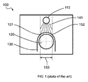
図1は、当技術分野で知られている堆積装置を示す。堆積装置100は、回転可能なスパッタデバイス110および被覆ドラム120を提供する。ウエブ130などの被覆すべき基板が、被覆ドラムによって案内される。堆積装置の動作中、堆積させるべき材料、すなわち堆積材料が、スパッタデバイス110から放出される。粒子140がスパッタデバイスから広がり、ウエブ130上に堆積する。さらに、図1では被覆窓150を見ることができる。被覆窓は、被覆ドラム120の第1の位置151から被覆ドラム120の第2の位置152に及ぶ。被覆窓内では、堆積させる材料の約99%が、被覆すべき基板に到達する。
FIG. 1 shows a deposition apparatus known in the art. The
しかし、基板が丸い被覆ドラムの上を進んでいるため、ウエブ被覆プロセスにおける図1の堆積装置などのスパッタ区画は、制限された寸法を有する。小さいチャンバ寸法が望ましいため、被覆窓も制限された寸法を提供する。図1の例では、被覆窓は、基板平面内で約220mmの寸法を有する。すなわち、前述の堆積装置内では、収集効率、すなわち放出された材料が基板に到達する割合は、約30%である。スパッタデバイスから放出された材料の残りは無駄になる。約400mmの寸法まで被覆窓を広げることで、堆積効率を増大させることができるが、1つの堆積機械内のカソードの数を低減させる。したがって、いくつかの被覆装置を有する堆積機械の全体的な効率は低下することになる。さらに、ガラス基板など、堆積チャンバ内を案内されている平面の基板に対して2つのスパッタデバイスを使用することが知られている。しかし、空間的な制限により、ウエブ被覆プロセスで2つのスパッタデバイスを使用することはできない。 However, because the substrate is traveling over a round coating drum, the sputter section, such as the deposition apparatus of FIG. 1, in the web coating process has limited dimensions. Since small chamber dimensions are desirable, the coated window also provides limited dimensions. In the example of FIG. 1, the covering window has a dimension of about 220 mm in the substrate plane. That is, in the above-described deposition apparatus, the collection efficiency, that is, the rate at which the released material reaches the substrate is about 30%. The remainder of the material released from the sputter device is wasted. Widening the coating window to a dimension of about 400 mm can increase the deposition efficiency, but reduces the number of cathodes in one deposition machine. Thus, the overall efficiency of a deposition machine having several coating devices will be reduced. In addition, it is known to use two sputter devices for a planar substrate guided in a deposition chamber, such as a glass substrate. However, due to space limitations, two sputter devices cannot be used in the web coating process.
本明細書に記載する実施形態は、いくつかの堆積装置を有する堆積機械の全体的な効率を低下させることなく堆積装置の収集効率を増大させる堆積装置を提供する。本明細書に記載する実施形態によれば、被覆すべきウエブが被覆ドラムによって案内されるウエブ被覆プロセスに対して、ツインスパッタデバイスが使用される。標準的な回転可能なツインカソードは、ウエブ被覆装置の典型的なスパッタ区画内に収まらない。既知の回転可能なツインスパッタデバイスを設置するには、より大きなカソード区画が必要とされ、それによって1つの被覆ドラム上で堆積させることができる様々な層の量が低減される。これは経済的ではない。本明細書に記載する実施形態は、ウエブ被覆装置内でツインスパッタデバイスを使用することを可能にするツインスパッタデバイスの設計を提供する。したがって、本明細書に記載する実施形態による堆積装置は、ウエブ被覆装置のスパッタ区画内にうまく収まる小さい回転可能なツインカソードを提供する。さらに、回転可能なスパッタデバイス内の磁石システムは、堆積率をさらに改善するように適合されてもよい。 The embodiments described herein provide a deposition apparatus that increases the collection efficiency of the deposition apparatus without reducing the overall efficiency of a deposition machine having several deposition apparatuses. According to the embodiments described herein, a twin sputter device is used for a web coating process in which the web to be coated is guided by a coating drum. Standard rotatable twin cathodes do not fit within the typical sputter compartment of a web coater. Installing a known rotatable twin sputter device requires a larger cathode compartment, thereby reducing the amount of different layers that can be deposited on one coating drum. This is not economical. The embodiments described herein provide a twin sputter device design that allows the use of a twin sputter device in a web coating apparatus. Accordingly, the deposition apparatus according to the embodiments described herein provides a small rotatable twin cathode that fits well within the sputter compartment of the web coating apparatus. Furthermore, the magnet system in the rotatable sputter device may be adapted to further improve the deposition rate.
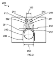
図2は、本明細書に記載する実施形態による堆積装置を示す。堆積装置200は、被覆ドラム220を提供し、被覆ドラム220上に、被覆すべき基板230が案内される。ツインスパッタデバイスをともに形成する第1のスパッタデバイス211および第2のスパッタデバイス212によって、堆積材料または堆積材料の成分が提供される。
FIG. 2 illustrates a deposition apparatus according to embodiments described herein. The
既知の回転可能なツインスパッタデバイス設計は、ウエブ被覆装置の区画の典型的な寸法内に収まらない。したがって、ウエブ被覆装置内の回転可能なツインスパッタデバイスがまだ利用可能ではなかったため、以前は平面のツインスパッタデバイスのみが使用された。したがって、本明細書に記載する実施形態は、ウエブ被覆装置に対する標準的なスパッタ区画内に収まる回転可能なツインスパッタデバイスの特別な設計について説明する。 Known rotatable twin sputter device designs do not fit within the typical dimensions of a web coater section. Thus, only a planar twin sputter device has been used previously because a rotatable twin sputter device in a web coater was not yet available. Thus, the embodiments described herein describe a special design of a rotatable twin sputter device that fits within a standard sputter compartment for a web coater.
図2に見ることができるように、第1のスパッタデバイス211は第1の軸213を有し、第1の軸213は、第1のスパッタデバイスの回転軸とすることができる。第2のスパッタデバイス212は第2の軸214を有し、第2の軸214もまた、第2のスパッタデバイスの回転軸とすることができる。これらのスパッタデバイスは、堆積材料、すなわち被覆すべき基板上に堆積させる材料を、ターゲットの形で提供する。反応性堆積プロセスの場合、基板上に最後に堆積させる材料は、処理ガスの化合物をさらに含むことができる。したがって、当業者であれば、たとえばシリコンまたはドープされたシリコンからなるターゲットは堆積材料としてシリコンを含み、例示的には、処理ガスとして酸素を添加して、最終的にSiO2を堆積させることができることを理解するであろう。
As can be seen in FIG. 2, the
図2に例示するいくつかの実施形態によれば、被覆すべき基板はウエブ230であり、ウエブは、ローラまたはドラム220によってツインスパッタデバイス211および212を通り過ぎて案内される。概して、被覆すべきウエブは、箔またはプラスチックのウエブなど、可撓性の構造を提供することができる。被覆窓250は、基板平面253に対して突出したドラム220上のウエブ230の第1の位置251および基板平面253に対して突出したドラム220上のウエブ230の第2の位置252によって制限される。さらに、被覆窓は、基板のうち材料が堆積する区域を画定する。図2に見ることができるように、第1のスパッタデバイス211から放出された堆積材料の粒子241および第2のスパッタデバイス212から放出された堆積材料の粒子242は、被覆窓250を通って基板230に到達する。図2に見ることができるように、被覆窓250は基板平面内で測定される。基板平面は、1つの点で基板に対して実質的に接線方向の平面253とすることができる。
According to some embodiments illustrated in FIG. 2, the substrate to be coated is a
本明細書に記載する実施形態による堆積装置200は、第1のスパッタデバイス211の第1の軸213から第2のスパッタデバイス212の第2の軸214までの約200mmより小さい距離260を提供するように適合される。典型的には、第1のスパッタデバイス211の第1の軸213から第2のスパッタデバイス212の第2の軸214までの距離260は、150mm〜200mm、より典型的には160mm〜190mm、さらに典型的には170mm〜185mm、たとえば180mmである。
The
図3は、本明細書に記載する実施形態による堆積装置の概略上面図を示す。堆積装置300は、図2に関して説明した堆積装置とすることができる。図3では、ツインスパッタデバイスを保持するスパッタデバイス支持体を見ることができる。特に、第1のスパッタデバイス支持体301が第1のスパッタデバイス311を保持し、第2のスパッタデバイス支持体302が第2のスパッタデバイス312を保持する。いくつかの実施形態によれば、第1のスパッタデバイス支持体301および第2のスパッタデバイス支持体302は、互いに対して画定された距離で第1のスパッタデバイス311および第2のスパッタデバイス312を保持するように適合されてもよい。たとえば、第1のスパッタデバイス支持体301および第2のスパッタデバイス支持体302は、これらのスパッタデバイス間で所望の距離を提供するように相互に連結することができる。他の実施形態によれば、堆積装置のスパッタデバイス支持体は、2つの区間、すなわち第1のスパッタデバイスに対する区間(第1のスパッタデバイス支持体など)と、第2のスパッタデバイスに対する区間(第2のスパッタデバイス支持体など)とに分割された1つのスパッタデバイス支持体とすることができる。概して、スパッタデバイス支持体は、スパッタデバイスを保持して回転させることを可能にする機構(図示せず)を有することができる。たとえば、スパッタデバイス支持体は軸受を提供することができ、軸受は、スパッタデバイスの回転を可能にするが、それと同時にスパッタデバイスの長手方向および径方向に対して画定された位置でスパッタデバイスを保持する。
FIG. 3 shows a schematic top view of a deposition apparatus according to embodiments described herein. The
いくつかの実施形態によれば、スパッタデバイス支持体は、第1のスパッタデバイスおよび第2のスパッタデバイスの軸を画定する。たとえば、スパッタデバイスを保持してこれらのスパッタデバイスの回転を同時に可能にすることによって、スパッタデバイス支持体は、第1のスパッタデバイスおよび第2のスパッタデバイスの回転軸を画定することができる。さらに、スパッタデバイス支持体は、スパッタデバイス間に画定された距離を提供する。図3では、第1のスパッタデバイス311の第1の軸313と第2のスパッタデバイス312の第2の軸314との間の距離360(スパッタデバイス支持体301および302によって画定される)は、約200mmより小さく、典型的には150mm〜200mm、より典型的には160mm〜190mm、さらに典型的には170mm〜185mm、たとえば180mmである。
According to some embodiments, the sputter device support defines an axis of the first sputter device and the second sputter device. For example, by holding the sputter devices and allowing these sputter devices to rotate simultaneously, the sputter device support can define the rotation axes of the first sputter device and the second sputter device. Further, the sputter device support provides a defined distance between the sputter devices. In FIG. 3, the distance 360 (defined by sputter device supports 301 and 302) between the
いくつかの実施形態によれば、第1のスパッタデバイスおよび第2のスパッタデバイスの外径は、典型的には約90mm〜約120mmの範囲、より典型的には約95mm〜約115mm、さらに典型的には約100mm〜約110mm、たとえば105mmとすることができる。概して、第1のスパッタデバイスおよび第2のスパッタデバイスの外径は、あらゆるスパッタリング動作が行われる前に決定することができる。さらに、スパッタデバイス支持体301および302は、図3に示すように、堆積プロセス前のスパッタデバイスの外面間の距離を指す距離370が、典型的には約50mm〜約100mmの範囲内、より典型的には約60mm〜約90mm、さらに典型的には約70mm〜約80mm、たとえば75mmになるように適合される。
According to some embodiments, the outer diameter of the first sputter device and the second sputter device typically ranges from about 90 mm to about 120 mm, more typically from about 95 mm to about 115 mm, and more typically Specifically, it can be about 100 mm to about 110 mm, for example, 105 mm. In general, the outer diameter of the first sputter device and the second sputter device can be determined before any sputtering operation is performed. In addition, the sputter device supports 301 and 302, as shown in FIG. 3, typically have a
図4では、堆積装置の概略側面図を見ることができる。堆積装置400は、図2または図3に関して説明した堆積装置とすることができる。図4の側面図は、堆積チャンバ400内のツインスパッタデバイスの第1のスパッタデバイス411を示す。スパッタデバイス支持体401は、スパッタデバイス411の軸413を画定する。さらに、被覆ドラム420を見ることができ、基板430がその上を案内されてもよい。図4の実施形態では、スパッタデバイス411の外面から被覆すべきウエブ430までの最短距離を指す距離480が示されている。ウエブとスパッタデバイスの表面との間の最短距離は、典型的には50mm〜200mm、より典型的には70mm〜190mm、さらに典型的には約80mm〜約180mmとすることができる。一実施形態では、スパッタデバイスの表面と被覆すべき表面との間の最短距離は、約100mmである。
In FIG. 4, a schematic side view of the deposition apparatus can be seen. The
これらの図では、スパッタデバイスは、基板より上に配向されている。しかし、これは単なる一例であり、スパッタデバイスおよび基板の配向は、別の方法で定めることができ、たとえばスパッタデバイスを基板の隣に配置することができ、またはスパッタデバイスより上で基板を案内することができることを理解されたい。 In these figures, the sputter device is oriented above the substrate. However, this is only an example, and the orientation of the sputter device and the substrate can be defined in another way, for example, the sputter device can be placed next to the substrate, or the substrate is guided above the sputter device Please understand that you can.
図5は、本発明の実施形態による堆積装置内で使用することができるツインスパッタデバイスおよびウエブを有する被覆ドラムの構成500を示す。第1のスパッタデバイス511および第2のスパッタデバイス512が設けられ、第1のスパッタデバイス511に対する第1の軸513および第2のスパッタデバイス513に対する第2の軸514に配置される。ツインスパッタデバイス511および512は、堆積させるべき材料または堆積させるべき材料の成分から作られたターゲットを含むことができ、被覆窓550を通って基板530に対する堆積材料を提供するように適合される。基板530は、被覆ドラム520によって案内することができる。被覆窓550は、ツインスパッタデバイスから放出された粒子540が基板に到達する区域によって画定される。被覆ドラム520が湾曲していることは、基板530の小さい区間のみがターゲット材料粒子540に露出されることを意味する。基板の小さい区間は、基板平面553に対して突出した被覆ドラム520上のウエブ530の第1の位置551および基板平面553に対して突出した被覆ドラム530上のウエブ530の第2の位置552によって制限することができる。第1の位置551および第2の位置552はまた、被覆窓550の始端および末端を指すことができる。いくつかの実施形態によれば、被覆窓550の寸法は、平面553などの基板平面内で測定することができ、平面553は、少なくとも1つの点で被覆ドラム520上の基板に対して実質的に接線方向である。基板に対して実質的に接線方向の基板平面553を形成することができる点は、基板のうちスパッタデバイスの少なくとも1つに対して最短距離を有する点とすることができる。
FIG. 5 illustrates a
さらに、いくつかの実施形態によれば、第1のスパッタデバイス511内に第1の磁石アレンジメント515が位置し、第2のスパッタデバイス512内に第2の磁石アレンジメント516が位置する。第1の磁石アレンジメントおよび第2の磁石アレンジメントはそれぞれ、磁場を生成する。磁石アレンジメント515および516によって生成される磁場は、概して、堆積効率を増大させるのに役立つ。さらに、スパッタデバイス内で磁石アレンジメントを使用することによって、堆積率に良い影響を与えることができる。
Further, according to some embodiments, a
図6では、ツインスパッタデバイス、被覆ドラム、および被覆すべき基板を含む構成600の一実施形態が示されている。構成600は、たとえば、図2〜図4に関して上記で説明した堆積装置内で使用することができる。構成600は、第1のスパッタデバイス611と、第2のスパッタデバイス612と、被覆ドラム620と、被覆すべき基板630とを含む。被覆すべき基板630は、被覆ドラム620上でスパッタデバイス611および612を通り過ぎて案内され、したがって被覆窓650を通過する。被覆窓650は、基板平面653に対して突出したドラム630上の基板620の第1の位置651および基板平面653に対して突出したドラム630上の基板620の第2の位置652によって制限される。被覆窓650を通って、ツインスパッタデバイスから放出された粒子640が基板620に到達する。
In FIG. 6, one embodiment of a
図6に示す実施形態では、第1のスパッタデバイス611は第1の磁石アレンジメント515を備え、第2のスパッタデバイス512は第2の磁石アレンジメント516を備える。磁石アレンジメント615および616は、それぞれ堆積効率を改善するために磁場を生成する磁石ヨークとすることができる。いくつかの実施形態によれば、これらの磁石アレンジメントは、互いの方へ傾斜させることができる。これは、磁石アレンジメント515および516によって図6に示されている。いくつかの実施形態によれば、これらの磁石アレンジメントは、第1のスパッタデバイス、第2のスパッタデバイス、第1の磁石アレンジメント、および/または第2の磁石アレンジメントをそれぞれ配置することによって、互いの方へ傾斜させることができる。
In the embodiment shown in FIG. 6, the
この文脈で、磁石アレンジメントが互いの方へ傾斜して配置されることは、磁石アレンジメントによって生成される磁場が互いの方へ誘導されることを意味する。たとえば、スパッタデバイスの回転軸から磁石アレンジメントまたは磁石アレンジメントの実質的に中心へ進む径方向軸は、他方のスパッタデバイスの対応する軸に対して角度を形成することができる。第1のスパッタデバイス611および第2のスパッタデバイス612の径方向軸は、図6に見ることができる。第1の径方向軸617は、第1のスパッタデバイス611の第1の回転軸613から第1の磁石アレンジメント615の中心へ延びる。第2の径方向軸618は、第2のスパッタデバイス612の第2の回転軸614から第2の磁石アレンジメント616の中心へ延びる。径方向軸617と径方向軸618との間には、磁石アレンジメントの互いの方への傾斜を示す角度619が示されている。いくつかの実施形態によれば、磁石アレンジメント間の角度、たとえば図6の角度619は、典型的には約5°〜約50°の範囲内、より典型的には約10°〜約40°、さらに典型的には約10°〜約30°とすることができる。
In this context, the arrangement of the magnet arrangements inclined towards each other means that the magnetic fields generated by the magnet arrangements are induced towards each other. For example, a radial axis that travels from the rotational axis of the sputter device to the magnet arrangement or substantially the center of the magnet arrangement can form an angle with respect to the corresponding axis of the other sputter device. The radial axes of the
いくつかの実施形態によれば、前述のスパッタデバイスを使用して、ウエブ上に絶縁材料を堆積させることができる。たとえば、スパッタデバイスは、シリコン、チタン、アルミニウムなどのターゲット材料を提供することができる。ガス入り口ともに、たとえば反応性スパッタリングプロセスによって、酸化ケイ素、窒化ケイ素、酸化チタン、酸化アルミニウムなどの材料を基板上に堆積させることができる。さらに、上記の堆積装置は、SiO2の反応性スパッタリングなどの反応性スパッタプロセスに使用することができる。したがって、本明細書に記載する他の実施形態と組み合わせることができるいくつかの実施形態によれば、堆積装置は、真空ポンプ、プロセスガス(酸素または窒素など)に対するガス入り口、加熱手段、冷却手段、ドライバなどのさらなる機器を備えることができる。 According to some embodiments, the aforementioned sputter device can be used to deposit an insulating material on the web. For example, a sputter device can provide a target material such as silicon, titanium, aluminum. Along with the gas inlet, materials such as silicon oxide, silicon nitride, titanium oxide, aluminum oxide can be deposited on the substrate, for example by a reactive sputtering process. Furthermore, the deposition apparatus described above can be used for reactive sputtering processes such as reactive sputtering of SiO 2 . Thus, according to some embodiments that can be combined with other embodiments described herein, the deposition apparatus comprises a vacuum pump, a gas inlet for a process gas (such as oxygen or nitrogen), a heating means, a cooling means. Additional devices such as drivers can be provided.
いくつかの実施形態によれば、上記の堆積装置および構成は、2つの金属スパッタデバイスが約10kHz〜約50kHzの周波数範囲などの中間周波数(MF)で動作するプロセスで使用することができる。一実施形態では、堆積装置および/または堆積装置のスパッタデバイス支持体は、スパッタデバイスのうちの一方をアノードとして使用し、他方をカソードとして使用するように適合されてもよい。概して、堆積装置は、アノードおよびカソードとしてのスパッタデバイスの動作を交互にすることができるように適合される。すなわち、前にアノードとして使用されているスパッタデバイスをカソードとして使用することができ、前にカソードとして使用されているスパッタデバイスをアノードとして動作させることができる。 According to some embodiments, the deposition apparatus and configuration described above can be used in processes where two metal sputter devices operate at an intermediate frequency (MF), such as a frequency range of about 10 kHz to about 50 kHz. In one embodiment, the deposition apparatus and / or sputter device support of the deposition apparatus may be adapted to use one of the sputter devices as an anode and the other as a cathode. In general, the deposition apparatus is adapted to be able to alternate the operation of the sputter device as the anode and cathode. That is, the sputter device previously used as the anode can be used as the cathode, and the sputter device previously used as the cathode can be operated as the anode.
一実施形態では、上記の堆積装置は、1つのスパッタデバイス支持体に対して1つのスパッタデバイスを設けることができる。すなわち、1つのスパッタデバイス支持体内に1つの回転可能なスパッタデバイスのみが設けられる。たとえば、第1のスパッタデバイス支持体内に1つの第1のスパッタデバイスが配置され、第2のスパッタデバイス支持体内に1つの第2のスパッタデバイスが配置される。いくつかの実施形態によれば、1対のツインスパッタデバイス、すなわち1つの第1のスパッタデバイスおよび1つの第2のスパッタデバイスが、1つの被覆窓に対して設けられる。堆積装置は、概して、いくつかの被覆窓を有することができ、各被覆窓に対して、それぞれ1つの第1のスパッタデバイスおよび1つの第2のスパッタデバイスのみを使用することができる。被覆窓は、堆積させるべき材料が基板に到達する区間として画定されると理解することができる。それによって、基板は、被覆窓を通過することによって第1のスパッタデバイスおよび第2のスパッタデバイスを通過する。 In one embodiment, the deposition apparatus described above can provide one sputter device for one sputter device support. That is, only one rotatable sputter device is provided in one sputter device support. For example, one first sputter device is disposed in the first sputter device support, and one second sputter device is disposed in the second sputter device support. According to some embodiments, a pair of twin sputter devices, one first sputter device and one second sputter device, are provided for one coated window. The deposition apparatus can generally have several coating windows, and only one first sputter device and one second sputter device can be used for each coating window. It can be understood that the coating window is defined as the section where the material to be deposited reaches the substrate. Thereby, the substrate passes through the first sputter device and the second sputter device by passing through the coating window.
図7は、本明細書に記載する実施形態によるウエブ上に堆積材料を堆積させる方法の流れ図を示す。いくつかの実施形態によれば、この方法は、図2〜図4に関して上述した堆積装置または図5および図6に示す構成を動作させるために使用することができる。この方法は、ブロック710で、被覆ドラム上で第1のスパッタデバイスおよび第2のスパッタデバイスを通り過ぎてウエブを案内することを含むことができる。いくつかの実施形態によれば、これらのスパッタデバイスは、ウエブなどの基板上に堆積させるべき材料を提供する上記のスパッタデバイスとすることができる。たとえば、本明細書に記載する実施形態によるウエブは、ブロック715に示すように、ツインスパッタデバイスを通過する。スパッタデバイスは、それぞれ回転軸を有する回転可能なスパッタデバイスとすることができる。いくつかの実施形態によれば、第1の回転可能なスパッタデバイスおよび第2の回転可能なスパッタデバイスは、図7にブロック720として示すように、第1のスパッタデバイスの回転軸と第2のスパッタデバイスの回転軸との間の距離が約200mmより小さくなるように配置される。いくつかの実施形態では、第1のスパッタデバイスの回転軸と第2のスパッタデバイスの回転軸との間の距離は、150mm〜200mm、より典型的には160mm〜190mm、さらに典型的には170mm〜185mm、たとえば180mmである。
FIG. 7 shows a flow diagram of a method for depositing a deposition material on a web according to embodiments described herein. According to some embodiments, the method can be used to operate the deposition apparatus described above with respect to FIGS. 2-4 or the configurations shown in FIGS. The method can include, at
さらに、本明細書に記載する実施形態による方法は、ブロック730で、第1のスパッタデバイスおよび第2のスパッタデバイスからの堆積材料でウエブを被覆することを含む。概して、ウエブ上に堆積させる材料は、スパッタデバイスから放出され、1つの被覆窓内でウエブ上に堆積する。被覆窓は、基板平面内で堆積材料が通過して基板に到達する区間として画定することができる。ウエブが被覆窓を通過するとき、ウエブは、スパッタデバイスから放出された粒子に露出される。いくつかの実施形態によれば、ウエブが被覆ドラム上で第1のスパッタデバイスおよび第2の回転可能なスパッタデバイスを通り過ぎて案内される間に、被覆が行われる。
Further, the method according to embodiments described herein includes coating the web with deposition material from the first sputter device and the second sputter device at
いくつかの実施形態によれば、被覆窓は、基板平面内で典型的には約150mm〜約250mm、より典型的には約180mm〜約240mm、さらに典型的には約200mm〜230mm、たとえば220mmの寸法を有することができる。被覆窓の幅は、基板平面に対して突出して被覆窓を制限する被覆ドラム上の第1の位置および第2の位置によってさらに画定することができる。たとえば、被覆窓の幅は、図2〜図6で被覆窓250、350、450、550、および650として見ることができる。
According to some embodiments, the coated window is typically about 150 mm to about 250 mm, more typically about 180 mm to about 240 mm, more typically about 200 mm to 230 mm, such as 220 mm in the substrate plane. Can have the following dimensions: The width of the coating window can be further defined by a first position and a second position on the coating drum that project relative to the substrate plane to limit the coating window. For example, the width of the covering window can be seen as covering
本明細書に記載する実施形態による方法は、第1のスパッタデバイスおよび第2のスパッタデバイスのうちの一方をアノードとして使用し、第1のスパッタデバイスおよび第2のスパッタデバイスのうちの他方をカソードとして使用することをさらに含むことができる。本明細書に記載する他の実施形態と組み合わせることができる本明細書に記載するいくつかの実施形態によれば、堆積装置、特に堆積装置のスパッタデバイス支持体は、対応する機能を提供するように適合することができ、すなわち一方のスパッタデバイスをアノードとして、他方のスパッタデバイスをカソードとして、交互に使用することを可能にする。 A method according to embodiments described herein uses one of a first sputter device and a second sputter device as an anode and the other of a first sputter device and a second sputter device as a cathode. Can be further included. According to some embodiments described herein that can be combined with other embodiments described herein, the deposition apparatus, particularly the sputter device support of the deposition apparatus, provides a corresponding function. That is, it is possible to use one sputter device as an anode and the other as a cathode alternately.
一実施形態では、ウエブ上に材料を堆積させる方法は、第1のスパッタデバイス内の第1の磁石アレンジメントによって第1の磁場を生成し、第2のスパッタデバイス内の第2の磁石アレンジメントによって第2の磁場を生成することをさらに含む。上記の構成は、図5に例示されている。さらに、いくつかの実施形態によれば、これらの磁石アレンジメントは、第1のスパッタデバイス、第2のスパッタデバイス、第1の磁石アレンジメント、および/または第2の磁石アレンジメントをそれぞれ配置することによって、互いの方へ傾斜させて配置することができる。そのような構成は図6に示されており、径方向軸617および618は、角度619とともに、傾斜した構成を示す。
In one embodiment, a method of depositing material on a web generates a first magnetic field with a first magnet arrangement in a first sputter device and a first magnet arrangement in a second sputter device. Further comprising generating two magnetic fields. The above configuration is illustrated in FIG. Further, according to some embodiments, these magnet arrangements are arranged by placing a first sputter device, a second sputter device, a first magnet arrangement, and / or a second magnet arrangement, respectively. They can be tilted towards each other. Such a configuration is shown in FIG. 6, with
本明細書に記載する実施形態による堆積装置および堆積材料を堆積させる方法を使用することで、高いスパッタデバイスの利用率(最大約80%)および再堆積のない浸食プロファイルが可能になる。これにより、材料コストが節約され、プロセスがより効率的になる。さらに、ウエブ被覆装置で使用される上向きのスパッタを利用した場合、粒子がスパッタデバイス上に落下する可能性がなく、それによってアークを発生させ、したがって層の特性を制限することがないため、スパッタプロセスの品質を改善することができる。さらに、本明細書に記載する実施形態は、スパッタカソードに対して制限された寸法を有し、空間的な制限のために回転可能なツインスパッタデバイスを使用することができないシステムにも適用することができる。 Using the deposition apparatus and method of depositing deposition material according to embodiments described herein allows for high sputter device utilization (up to about 80%) and erosion profiles without redeposition. This saves material costs and makes the process more efficient. In addition, when utilizing the upward sputter used in web coating equipment, there is no possibility of particles falling onto the sputter device, thereby generating an arc and thus not limiting the properties of the layer. Process quality can be improved. Further, the embodiments described herein also apply to systems that have limited dimensions with respect to the sputter cathode and cannot use a rotatable twin sputter device due to space limitations. Can do.
一態様では、ウエブ上に堆積材料を堆積させる堆積装置が提供される。堆積装置は、第1の回転可能なスパッタデバイスに対する第1の軸を画定する第1のスパッタデバイス支持体と、第2の回転可能なスパッタデバイスに対する第2の軸を画定する第2のスパッタデバイス支持体と、被覆窓とを含むことができる。いくつかの実施形態によれば、第1のスパッタデバイス支持体および第2のスパッタデバイス支持体は、被覆ドラムの上のウエブ上に堆積させるべき堆積材料を提供するために第1の回転可能なスパッタデバイスおよび第2の回転可能なスパッタデバイスを支持するように適合される。第1の軸と第2の軸との間の距離は、約200mmより小さくすることができる。さらに、本明細書に記載する他の実施形態と組み合わせることができるいくつかの実施形態によれば、堆積装置は、第1の回転可能なスパッタデバイスおよび第2の回転可能なスパッタデバイスのうちの一方の回転可能なスパッタデバイスをアノードとして使用し、第1の回転可能なスパッタデバイスおよび第2の回転可能なスパッタデバイスのうちの他方の回転可能なスパッタデバイスをカソードとして使用するように適合されてもよい。一実施形態では、堆積装置は、第1の回転可能なスパッタデバイスおよび第2の回転可能なスパッタデバイスをさらに含むことができる。本明細書に記載する他の実施形態と組み合わせることができるいくつかの実施形態によれば、第1の磁場を生成する第1の磁石アレンジメントを第1の回転可能なスパッタデバイス内に配置することができ、第2の磁場を生成する第2の磁石アレンジメントを第2の回転可能なスパッタデバイス内に配置することができる。第1の磁石アレンジメントおよび第2の磁石アレンジメントは、被覆窓内の堆積材料の堆積を増大させるようにさらに適合されてもよい。一実施形態では、第1の磁石アレンジメントおよび第2の磁石アレンジメントが互いの方へ傾斜して配置されるように、第1の回転可能なスパッタデバイスおよび第2の回転可能なスパッタデバイスを配置することができる。本明細書に記載する他の実施形態と組み合わせることができるいくつかの実施形態によれば、第1のスパッタデバイス支持体および第2のスパッタデバイス支持体のうちの少なくとも1つは、約100mmと約120mmの間、特に約105mmの外径を有する回転可能なスパッタデバイスを保持するように適合されてもよい。さらに、一実施形態では、第1のスパッタデバイス支持体および第2のスパッタデバイス支持体は、1つの被覆窓に対して、第1のスパッタデバイス支持体内に1つの第1の回転可能なスパッタデバイスのみを提供し、第2のスパッタデバイス支持体内に1つの第2の回転可能なスパッタデバイスのみを提供するように適合されてもよい。さらなる実施形態によれば、第1のスパッタデバイス支持体は第1のスパッタデバイスを保持するように適合され、第2のスパッタデバイス支持体は第2のスパッタデバイスを保持するように適合され、第1のスパッタデバイスおよび第2のスパッタデバイスはツインスパッタデバイスである。概して、被覆窓は、約200mmと約250mmの間、特に約220mmの幅を提供することができる。本明細書に記載する他の実施形態と組み合わせることができる一実施形態では、堆積させるべき材料は、絶縁材料とすることができる。たとえば、堆積させるべき材料は、酸化ケイ素、窒化ケイ素、酸化チタン、および酸化アルミニウムの群から選択することができる。 In one aspect, a deposition apparatus is provided for depositing a deposition material on a web. The deposition apparatus includes a first sputter device support that defines a first axis for the first rotatable sputter device and a second sputter device that defines a second axis for the second rotatable sputter device. A support and a coated window can be included. According to some embodiments, the first sputter device support and the second sputter device support are first rotatable to provide a deposition material to be deposited on the web on the coating drum. Adapted to support the sputter device and the second rotatable sputter device. The distance between the first axis and the second axis can be less than about 200 mm. Further, according to some embodiments that can be combined with other embodiments described herein, the deposition apparatus includes a first rotatable sputter device and a second rotatable sputter device. Adapted to use one rotatable sputter device as the anode and the other rotatable sputter device of the first rotatable sputter device and the second rotatable sputter device as the cathode. Also good. In one embodiment, the deposition apparatus can further include a first rotatable sputter device and a second rotatable sputter device. According to some embodiments that can be combined with other embodiments described herein, a first magnet arrangement that generates a first magnetic field is disposed within a first rotatable sputter device. And a second magnet arrangement for generating a second magnetic field can be disposed in the second rotatable sputter device. The first magnet arrangement and the second magnet arrangement may be further adapted to increase the deposition of deposition material within the coating window. In one embodiment, the first rotatable sputter device and the second rotatable sputter device are arranged such that the first magnet arrangement and the second magnet arrangement are inclined toward each other. be able to. According to some embodiments that can be combined with other embodiments described herein, at least one of the first sputter device support and the second sputter device support is about 100 mm and It may be adapted to hold a rotatable sputter device having an outer diameter between about 120 mm, in particular about 105 mm. Further, in one embodiment, the first sputter device support and the second sputter device support are one first rotatable sputter device within the first sputter device support relative to one coating window. May be adapted to provide only one second rotatable sputter device within the second sputter device support. According to a further embodiment, the first sputter device support is adapted to hold the first sputter device, the second sputter device support is adapted to hold the second sputter device, The first sputter device and the second sputter device are twin sputter devices. In general, the coated window can provide a width of between about 200 mm and about 250 mm, especially about 220 mm. In one embodiment that can be combined with other embodiments described herein, the material to be deposited can be an insulating material. For example, the material to be deposited can be selected from the group of silicon oxide, silicon nitride, titanium oxide, and aluminum oxide.
さらなる態様では、ウエブ上に堆積材料を堆積させる方法が提供される。この方法は、被覆ドラム上で第1のスパッタデバイスおよび第2のスパッタデバイスを通り過ぎてウエブを案内することを含むことができ、第1のスパッタデバイスおよび第2のスパッタデバイスは、回転可能なツインスパッタデバイスであり、堆積材料または堆積材料の成分を提供する。さらに、第1の回転可能なスパッタデバイスおよび第2の回転可能なスパッタデバイスは、第1のスパッタデバイスの回転軸と第2のスパッタデバイスの回転軸との間の距離が約200mmより小さくなるように配置することができる。この方法は、第1の回転可能なスパッタデバイスおよび第2の回転可能なスパッタデバイスを通り過ぎてウエブを案内しながら1回の被覆でウエブを堆積材料で被覆することをさらに含むことができる。いくつかの実施形態によれば、ウエブを被覆することは、約220mmの被覆窓内でウエブを被覆することを含む。本明細書に記載する他の実施形態と組み合わせることができる一実施形態では、この方法は、第1のスパッタデバイスおよび第2のスパッタデバイスのうちの一方をアノードとして使用し、第1のスパッタデバイスおよび第2のスパッタデバイスのうちの他方をカソードとして使用することをさらに含む。いくつかの実施形態によれば、材料を堆積させる方法は、第1のスパッタデバイス内の第1の磁石アレンジメントによって第1の磁場を生成し、第2のスパッタデバイス内の第2の磁石アレンジメントによって第2の磁場を生成することをさらに含むことができる。概して、第1の磁石アレンジメントおよび第2の磁石アレンジメントが互いの方へ傾斜して配置されるように、第1のスパッタデバイス、第2のスパッタデバイス、第1の磁石アレンジメント、および第2の磁石アレンジメントのうちの少なくとも1つを配置することができる。 In a further aspect, a method for depositing a deposition material on a web is provided. The method can include guiding the web past the first sputter device and the second sputter device on the coating drum, wherein the first sputter device and the second sputter device are rotatable twins. A sputter device that provides a deposition material or a component of a deposition material. Further, the first rotatable sputter device and the second rotatable sputter device are such that the distance between the rotation axis of the first sputter device and the rotation axis of the second sputter device is less than about 200 mm. Can be arranged. The method can further include coating the web with the deposition material in a single coating while guiding the web past the first rotatable sputter device and the second rotatable sputter device. According to some embodiments, coating the web includes coating the web within an approximately 220 mm coating window. In one embodiment that can be combined with other embodiments described herein, the method uses one of the first sputter device and the second sputter device as an anode and the first sputter device. And using the other of the second sputter devices as a cathode. According to some embodiments, a method of depositing a material generates a first magnetic field by a first magnet arrangement in a first sputter device and by a second magnet arrangement in a second sputter device. It can further include generating a second magnetic field. In general, the first sputter device, the second sputter device, the first magnet arrangement, and the second magnet such that the first magnet arrangement and the second magnet arrangement are arranged inclined toward each other. At least one of the arrangements can be arranged.
上記は本発明の実施形態を対象とするが、本発明の基本的な範囲から逸脱することなく、本発明の他のさらなる実施形態を考案することもでき、本発明の範囲は、以下の特許請求の範囲によって決定される。 While the above is directed to embodiments of the present invention, other and further embodiments of the invention may be devised without departing from the basic scope thereof, and the scope of the invention is subject to the following patents: Determined by the claims.
Claims (14)
堆積材料の一部を遮蔽するマスク又は遮蔽部分によって前記被覆窓が画定され、
前記第1のスパッタデバイス支持体および前記第2のスパッタデバイス支持体が、前記被覆ドラムの上の前記ウエブ上に堆積させるべき少なくとも前記堆積材料の成分を提供するために前記第1の回転可能なスパッタデバイスおよび前記第2の回転可能なスパッタデバイスを支持するように適合され、
前記第1のスパッタデバイス支持体および前記第2のスパッタデバイス支持体は、1つの被覆窓に対して、前記第1のスパッタデバイス支持体内に1つの第1の回転可能なスパッタデバイスのみを提供し、前記第2のスパッタデバイス支持体内に1つの第2の回転可能なスパッタデバイスのみを提供するように適合され、
前記第1の軸と前記第2の軸との間の距離が150mmと200mmの間であり、前記被覆窓の幅は、200mmと250mmの間である、堆積装置。 A deposition apparatus for depositing deposition material on a web, the first sputter device support defining a first axis for a first rotatable sputter device and a second for a second rotatable sputter device. A second sputter device support defining an axis of the coating, a coating drum for guiding the web to be coated, and a coating window;
The covering window is defined by a mask or shielding portion that shields a portion of the deposited material;
The first sputtering device support and the second sputtering device support is rotatable first to provide at least a component of the deposition material to be deposited on said web on said cover drum Adapted to support a sputter device and said second rotatable sputter device;
The first sputter device support and the second sputter device support provide only one first rotatable sputter device in the first sputter device support for one coating window. Adapted to provide only one second rotatable sputter device within the second sputter device support;
The deposition apparatus , wherein the distance between the first axis and the second axis is between 150 mm and 200 mm, and the width of the covering window is between 200 mm and 250 mm .
被覆ドラム上で第1のスパッタデバイスおよび第2のスパッタデバイスを通り過ぎて前記ウエブを案内することを含み、前記第1のスパッタデバイスおよび前記第2のスパッタデバイスが、200mmと250mmの間の幅の1つの被覆窓に提供される回転可能なツインスパッタデバイスであり、堆積材料の一部を遮蔽するマスク又は遮蔽部分によって前記被覆窓が画定され、前記第1のスパッタデバイスおよび前記第2のスパッタデバイスが、少なくとも前記堆積材料の成分を提供し、前記第1のスパッタデバイスの回転軸と前記第2のスパッタデバイスの回転軸との間の距離が200mmより小さくなるように、前記第1の回転可能なスパッタデバイスおよび前記第2の回転可能なスパッタデバイスが配置され、
前記第1の回転可能なスパッタデバイスおよび前記第2の回転可能なスパッタデバイスを通り過ぎて前記ウエブを案内しながら1回の被覆で前記ウエブを堆積材料で被覆することとを含む方法。 A method of depositing a deposition material on a web, comprising:
On coating drum past the first sputtering device and a second sputtering device the method comprising guiding the web, the first sputter device and the second sputtering device, the width between 200mm and 250mm A rotatable twin sputter device provided on one coating window, the coating window being defined by a mask or shielding portion that shields a portion of the deposited material, the first sputter device and the second sputter device but at least to provide the components of the deposition material, the so that the distance between the rotation axis of said the rotational axis of the first sputtering device second sputtering device is less than 200 mm, the first rotatable A second sputter device and a second rotatable sputter device ,
Coating the web with a deposition material in a single coating while guiding the web past the first rotatable sputter device and the second rotatable sputter device.
Applications Claiming Priority (1)
| Application Number | Priority Date | Filing Date | Title |
|---|---|---|---|
| PCT/EP2012/054261 WO2013135265A1 (en) | 2012-03-12 | 2012-03-12 | Mini rotatable sputter devices for sputter deposition |
Publications (3)
| Publication Number | Publication Date |
|---|---|
| JP2015511667A JP2015511667A (en) | 2015-04-20 |
| JP2015511667A5 JP2015511667A5 (en) | 2015-05-28 |
| JP6073383B2 true JP6073383B2 (en) | 2017-02-01 |
Family
ID=45852532
Family Applications (1)
| Application Number | Title | Priority Date | Filing Date |
|---|---|---|---|
| JP2014561293A Expired - Fee Related JP6073383B2 (en) | 2012-03-12 | 2012-03-12 | Small rotatable sputter device for sputter deposition |
Country Status (7)
| Country | Link |
|---|---|
| US (1) | US20160189939A1 (en) |
| EP (1) | EP2826057B1 (en) |
| JP (1) | JP6073383B2 (en) |
| KR (1) | KR101780466B1 (en) |
| CN (1) | CN104160471B (en) |
| TW (1) | TWI567216B (en) |
| WO (1) | WO2013135265A1 (en) |
Families Citing this family (7)
| Publication number | Priority date | Publication date | Assignee | Title |
|---|---|---|---|---|
| KR101950857B1 (en) * | 2015-06-05 | 2019-02-21 | 어플라이드 머티어리얼스, 인코포레이티드 | Sputter deposition source, sputtering apparatus and method of operating thereof |
| US20180312964A1 (en) * | 2015-06-16 | 2018-11-01 | Schneider Gmbh & Co. Kg | Device, method and use for the coating of lenses |
| KR102407392B1 (en) * | 2015-07-03 | 2022-06-13 | 삼성디스플레이 주식회사 | Sputtering apparatus and sputtering method using the same |
| DE102016125278A1 (en) | 2016-12-14 | 2018-06-14 | Schneider Gmbh & Co. Kg | Apparatus, method and use for coating lenses |
| CN107354443B (en) * | 2017-07-26 | 2019-10-11 | 中国电子科技集团公司第五十五研究所 | A kind of device adjusting magnetron sputtering film uniformity |
| CN109487225A (en) * | 2019-01-07 | 2019-03-19 | 成都中电熊猫显示科技有限公司 | Magnetron sputtering film formation device and method |
| BE1027427B1 (en) * | 2019-07-14 | 2021-02-08 | Soleras Advanced Coatings Bv | Motion systems for sputter coating non-planar substrates |
Family Cites Families (10)
| Publication number | Priority date | Publication date | Assignee | Title |
|---|---|---|---|---|
| DE19610253C2 (en) * | 1996-03-15 | 1999-01-14 | Fraunhofer Ges Forschung | Atomizing device |
| WO2000028104A1 (en) * | 1998-11-06 | 2000-05-18 | Scivac | Sputtering apparatus and process for high rate coatings |
| DE10145201C1 (en) * | 2001-09-13 | 2002-11-21 | Fraunhofer Ges Forschung | Device for coating substrates having a curved surface contains a pair of rectangular magnetron sources and substrate holders arranged in an evacuated chamber |
| EP1856712A2 (en) * | 2005-01-13 | 2007-11-21 | Cardinal CG Company | Reduced maintenance sputtering chambers |
| JP2008038192A (en) * | 2006-08-04 | 2008-02-21 | Optorun Co Ltd | Sputtering source, sputtering film deposition apparatus and sputtering film deposition method |
| JP2009024230A (en) * | 2007-07-20 | 2009-02-05 | Kobe Steel Ltd | Sputtering apparatus |
| WO2010106432A2 (en) * | 2009-03-20 | 2010-09-23 | Applied Materials, Inc. | Deposition apparatus with high temperature rotatable target and method of operating thereof |
| JP5240782B2 (en) * | 2009-05-18 | 2013-07-17 | 株式会社神戸製鋼所 | Continuous film deposition system |
| EP2306489A1 (en) * | 2009-10-02 | 2011-04-06 | Applied Materials, Inc. | Method for coating a substrate and coater |
| US9394603B2 (en) * | 2010-11-17 | 2016-07-19 | Soleras Advanced Coatings Bvba | Soft sputtering magnetron system |
-
2012
- 2012-03-12 EP EP12709309.4A patent/EP2826057B1/en not_active Not-in-force
- 2012-03-12 JP JP2014561293A patent/JP6073383B2/en not_active Expired - Fee Related
- 2012-03-12 KR KR1020147028546A patent/KR101780466B1/en active IP Right Grant
- 2012-03-12 US US14/384,287 patent/US20160189939A1/en not_active Abandoned
- 2012-03-12 CN CN201280071216.6A patent/CN104160471B/en not_active Expired - Fee Related
- 2012-03-12 WO PCT/EP2012/054261 patent/WO2013135265A1/en active Application Filing
-
2013
- 2013-03-12 TW TW102108667A patent/TWI567216B/en not_active IP Right Cessation
Also Published As
| Publication number | Publication date |
|---|---|
| CN104160471A (en) | 2014-11-19 |
| KR20140138908A (en) | 2014-12-04 |
| TW201348482A (en) | 2013-12-01 |
| JP2015511667A (en) | 2015-04-20 |
| WO2013135265A1 (en) | 2013-09-19 |
| CN104160471B (en) | 2017-11-28 |
| EP2826057B1 (en) | 2018-01-24 |
| EP2826057A1 (en) | 2015-01-21 |
| US20160189939A1 (en) | 2016-06-30 |
| KR101780466B1 (en) | 2017-09-21 |
| TWI567216B (en) | 2017-01-21 |
Similar Documents
| Publication | Publication Date | Title |
|---|---|---|
| JP6073383B2 (en) | Small rotatable sputter device for sputter deposition | |
| KR101708194B1 (en) | Method for coating a substrate and coater | |
| TWI557252B (en) | Cathode assembly for a sputter deposition apparatus and method for depositing a film on a substrate in a sputter deposition apparatus | |
| JP6963551B2 (en) | Vacuum processing equipment and methods for processing substrates | |
| JP6134815B2 (en) | Apparatus using adjacent sputter cathode and operation method thereof | |
| EP2855729B1 (en) | Method for coating a substrate and coater | |
| KR20130100325A (en) | Systems and methods for forming a layer of sputtered material | |
| TW201608044A (en) | Sputter deposition apparatus and method for coating a substrate by rotary target assemblies in two coating regions and use thereof | |
| TW200902743A (en) | Swinging magnets to improve target utilization | |
| US20150021166A1 (en) | Sputtering apparatus and method | |
| JP6396367B2 (en) | Multi-directional racetrack rotating cathode for PVD arrays | |
| TW201617469A (en) | Target arrangement, processing apparatus with target arrangement and method for manufacturing a tagret arrangement | |
| TW201538768A (en) | Electrode assembly for deposition apparatus and method for assembling an electrode assembly | |
| JP2006176862A (en) | Sputtering film deposition system and sputtering film deposition method | |
| WO2020001762A1 (en) | Deposition apparatus, deposition system, and method of depositing a seed layer | |
| JP4877058B2 (en) | Opposing target sputtering apparatus and method | |
| KR20200020868A (en) | Movable Masking Element | |
| WO2016050284A1 (en) | Cathode sputtering mode |
Legal Events
| Date | Code | Title | Description |
|---|---|---|---|
| A521 | Request for written amendment filed |
Free format text: JAPANESE INTERMEDIATE CODE: A523 Effective date: 20150312 |
|
| A621 | Written request for application examination |
Free format text: JAPANESE INTERMEDIATE CODE: A621 Effective date: 20150312 |
|
| A977 | Report on retrieval |
Free format text: JAPANESE INTERMEDIATE CODE: A971007 Effective date: 20151221 |
|
| A131 | Notification of reasons for refusal |
Free format text: JAPANESE INTERMEDIATE CODE: A131 Effective date: 20160202 |
|
| A601 | Written request for extension of time |
Free format text: JAPANESE INTERMEDIATE CODE: A601 Effective date: 20160426 |
|
| A521 | Request for written amendment filed |
Free format text: JAPANESE INTERMEDIATE CODE: A523 Effective date: 20160623 |
|
| TRDD | Decision of grant or rejection written | ||
| A01 | Written decision to grant a patent or to grant a registration (utility model) |
Free format text: JAPANESE INTERMEDIATE CODE: A01 Effective date: 20161206 |
|
| A61 | First payment of annual fees (during grant procedure) |
Free format text: JAPANESE INTERMEDIATE CODE: A61 Effective date: 20170104 |
|
| R150 | Certificate of patent or registration of utility model |
Ref document number: 6073383 Country of ref document: JP Free format text: JAPANESE INTERMEDIATE CODE: R150 |
|
| R250 | Receipt of annual fees |
Free format text: JAPANESE INTERMEDIATE CODE: R250 |
|
| LAPS | Cancellation because of no payment of annual fees |