JP6062149B2 - Light emitting device and light emitting device package - Google Patents

Light emitting device and light emitting device package Download PDF

Info

Publication number
JP6062149B2
JP6062149B2 JP2012005901A JP2012005901A JP6062149B2 JP 6062149 B2 JP6062149 B2 JP 6062149B2 JP 2012005901 A JP2012005901 A JP 2012005901A JP 2012005901 A JP2012005901 A JP 2012005901A JP 6062149 B2 JP6062149 B2 JP 6062149B2
Authority
JP
Japan
Prior art keywords
layer
light emitting
semiconductor layer
emitting structure
contact
Prior art date
Legal status (The legal status is an assumption and is not a legal conclusion. Google has not performed a legal analysis and makes no representation as to the accuracy of the status listed.)
Active
Application number
JP2012005901A
Other languages
Japanese (ja)
Other versions
JP2013046050A (en
Inventor
チョン・ファンヒー
Current Assignee (The listed assignees may be inaccurate. Google has not performed a legal analysis and makes no representation or warranty as to the accuracy of the list.)
LG Innotek Co Ltd
Original Assignee
LG Innotek Co Ltd
Priority date (The priority date is an assumption and is not a legal conclusion. Google has not performed a legal analysis and makes no representation as to the accuracy of the date listed.)
Filing date
Publication date
Priority claimed from KR1020110083722A external-priority patent/KR20130021299A/en
Priority claimed from KR1020110114385A external-priority patent/KR101956016B1/en
Application filed by LG Innotek Co Ltd filed Critical LG Innotek Co Ltd
Publication of JP2013046050A publication Critical patent/JP2013046050A/en
Application granted granted Critical
Publication of JP6062149B2 publication Critical patent/JP6062149B2/en
Active legal-status Critical Current
Anticipated expiration legal-status Critical

Links

Images

Classifications

    • HELECTRICITY
    • H01ELECTRIC ELEMENTS
    • H01LSEMICONDUCTOR DEVICES NOT COVERED BY CLASS H10
    • H01L27/00Devices consisting of a plurality of semiconductor or other solid-state components formed in or on a common substrate
    • H01L27/15Devices consisting of a plurality of semiconductor or other solid-state components formed in or on a common substrate including semiconductor components having potential barriers, specially adapted for light emission
    • H01L27/153Devices consisting of a plurality of semiconductor or other solid-state components formed in or on a common substrate including semiconductor components having potential barriers, specially adapted for light emission in a repetitive configuration, e.g. LED bars
    • HELECTRICITY
    • H01ELECTRIC ELEMENTS
    • H01LSEMICONDUCTOR DEVICES NOT COVERED BY CLASS H10
    • H01L2924/00Indexing scheme for arrangements or methods for connecting or disconnecting semiconductor or solid-state bodies as covered by H01L24/00
    • H01L2924/0001Technical content checked by a classifier
    • H01L2924/0002Not covered by any one of groups H01L24/00, H01L24/00 and H01L2224/00
    • HELECTRICITY
    • H01ELECTRIC ELEMENTS
    • H01LSEMICONDUCTOR DEVICES NOT COVERED BY CLASS H10
    • H01L33/00Semiconductor devices having potential barriers specially adapted for light emission; Processes or apparatus specially adapted for the manufacture or treatment thereof or of parts thereof; Details thereof
    • H01L33/005Processes
    • H01L33/0093Wafer bonding; Removal of the growth substrate
    • HELECTRICITY
    • H01ELECTRIC ELEMENTS
    • H01LSEMICONDUCTOR DEVICES NOT COVERED BY CLASS H10
    • H01L33/00Semiconductor devices having potential barriers specially adapted for light emission; Processes or apparatus specially adapted for the manufacture or treatment thereof or of parts thereof; Details thereof
    • H01L33/02Semiconductor devices having potential barriers specially adapted for light emission; Processes or apparatus specially adapted for the manufacture or treatment thereof or of parts thereof; Details thereof characterised by the semiconductor bodies
    • H01L33/20Semiconductor devices having potential barriers specially adapted for light emission; Processes or apparatus specially adapted for the manufacture or treatment thereof or of parts thereof; Details thereof characterised by the semiconductor bodies with a particular shape, e.g. curved or truncated substrate
    • H01L33/22Roughened surfaces, e.g. at the interface between epitaxial layers
    • HELECTRICITY
    • H01ELECTRIC ELEMENTS
    • H01LSEMICONDUCTOR DEVICES NOT COVERED BY CLASS H10
    • H01L33/00Semiconductor devices having potential barriers specially adapted for light emission; Processes or apparatus specially adapted for the manufacture or treatment thereof or of parts thereof; Details thereof
    • H01L33/36Semiconductor devices having potential barriers specially adapted for light emission; Processes or apparatus specially adapted for the manufacture or treatment thereof or of parts thereof; Details thereof characterised by the electrodes
    • H01L33/38Semiconductor devices having potential barriers specially adapted for light emission; Processes or apparatus specially adapted for the manufacture or treatment thereof or of parts thereof; Details thereof characterised by the electrodes with a particular shape
    • H01L33/385Semiconductor devices having potential barriers specially adapted for light emission; Processes or apparatus specially adapted for the manufacture or treatment thereof or of parts thereof; Details thereof characterised by the electrodes with a particular shape the electrode extending at least partially onto a side surface of the semiconductor body
    • HELECTRICITY
    • H01ELECTRIC ELEMENTS
    • H01LSEMICONDUCTOR DEVICES NOT COVERED BY CLASS H10
    • H01L33/00Semiconductor devices having potential barriers specially adapted for light emission; Processes or apparatus specially adapted for the manufacture or treatment thereof or of parts thereof; Details thereof
    • H01L33/48Semiconductor devices having potential barriers specially adapted for light emission; Processes or apparatus specially adapted for the manufacture or treatment thereof or of parts thereof; Details thereof characterised by the semiconductor body packages
    • H01L33/62Arrangements for conducting electric current to or from the semiconductor body, e.g. lead-frames, wire-bonds or solder balls

Landscapes

  • Engineering & Computer Science (AREA)
  • Power Engineering (AREA)
  • Physics & Mathematics (AREA)
  • Condensed Matter Physics & Semiconductors (AREA)
  • General Physics & Mathematics (AREA)
  • Computer Hardware Design (AREA)
  • Microelectronics & Electronic Packaging (AREA)
  • Led Devices (AREA)
  • Led Device Packages (AREA)

Description

本発明の一実施例は、発光素子、発光素子パッケージ及びライトユニットに関する。   Embodiments described herein relate generally to a light emitting device, a light emitting device package, and a light unit.

発光素子の一つとして発光ダイオード(LED:Light Emitting Diode)がたくさん使われている。発光ダイオードは、化合物半導体の特性を利用して電気信号を赤外線、可視光線、紫外線のような光の形態に変換する。    A lot of light emitting diodes (LEDs) are used as one of the light emitting elements. A light emitting diode converts the electrical signal into a form of light such as infrared rays, visible rays, and ultraviolet rays by utilizing the characteristics of the compound semiconductor.

発光素子の光効率が増加されることによって表示装置、照明機器を含めた多様な分野に発光素子が適用されている。    As the light efficiency of the light emitting element is increased, the light emitting element is applied to various fields including a display device and a lighting device.

本発明の一実施例は、工程安全性が向上して電気的に連結された複数の発光セルを含む発光素子、発光素子パッケージ、ライトユニットを提供する。   An embodiment of the present invention provides a light emitting device, a light emitting device package, and a light unit including a plurality of light emitting cells that are electrically connected with improved process safety.

本発明の一実施例による発光素子は、支持基板と、前記支持基板上に配置された第1発光構造物であって、第1導電型の第1半導体層、前記第1半導体層の下の第1活性層、前記第1活性層の下の第2導電型の第2半導体層を有する第1発光構造物と、前記第1発光構造物の下の第1金属層と、前記支持基板上に配置された第2発光構造物であって、第1導電型の第3半導体層、前記第3半導体層の下の第2活性層、前記第2活性層の下の第2導電型の第4半導体層を有する第2発光構造物と、前記第2発光構造物の下の第2金属層と、前記第1半導体層の側面に接触して前記第2金属層と電気的に連結されたコンタクト部とを備える。   A light emitting device according to an embodiment of the present invention includes a support substrate and a first light emitting structure disposed on the support substrate, the first semiconductor layer having a first conductivity type, below the first semiconductor layer. A first light emitting structure having a first active layer, a second semiconductor layer of a second conductivity type under the first active layer, a first metal layer under the first light emitting structure, and on the support substrate A second light emitting structure disposed in a first conductive type third semiconductor layer, a second active layer under the third semiconductor layer, and a second conductive type second under the second active layer. A second light emitting structure having four semiconductor layers; a second metal layer under the second light emitting structure; and a side surface of the first semiconductor layer in contact with the second metal layer. A contact portion.

本発明の一実施例による発光素子は、第1導電型の第1半導体層、前記第1半導体層の下の第1活性層、前記第1活性層の下の第2導電型の第2半導体層を有する第1発光構造物と、前記第1発光構造物の下の第1金属層と、第1導電型の第3半導体層、前記第3半導体層の下の第2活性層、前記第2活性層の下の第2導電型の第4半導体層を有する第2発光構造物と、前記第2発光構造物の下の第2金属層と、前記第1半導体層に電気的に連結して前記第2金属層に電気的に連結されたコンタクト部と、前記第1金属層と前記第2金属層とを電気的に絶縁させて、前記コンタクト部と前記第1活性層との間を電気的に絶縁させて、前記コンタクト部と前記第2半導体層との間を電気的に絶縁させる絶縁層とを備える。   A light emitting device according to an embodiment of the present invention includes a first conductive type first semiconductor layer, a first active layer under the first semiconductor layer, and a second conductive type second semiconductor under the first active layer. A first light emitting structure having a layer; a first metal layer under the first light emitting structure; a third semiconductor layer of a first conductivity type; a second active layer under the third semiconductor layer; A second light emitting structure having a second semiconductor layer of a second conductivity type under the two active layers; a second metal layer under the second light emitting structure; and the first semiconductor layer electrically connected to the second light emitting structure. A contact portion electrically connected to the second metal layer, and the first metal layer and the second metal layer are electrically insulated from each other, and the contact portion and the first active layer are separated from each other. An insulating layer is provided that is electrically insulated to electrically insulate between the contact portion and the second semiconductor layer.

本発明の一実施例による発光素子パッケージは、胴体と、前記胴体の上に配置された発光素子と、前記発光素子に電気的に連結された第1リード電極及び第2リード電極とを備える。前記発光素子は、支持基板と、前記支持基板上に配置された第1発光構造物であって、第1導電型の第1半導体層、前記第1半導体層の下の第1活性層、前記第1活性層の下の第2導電型の第2半導体層を有する第1発光構造物と、前記第1発光構造物の下の第1金属層と、前記支持基板上に配置された第2発光構造物であって、第1導電型の第3半導体層、前記第3半導体層の下の第2活性層、前記第2活性層の下の第2導電型の第4半導体層を有する第2発光構造物と、前記第2発光構造物の下の第2金属層と、前記第1半導体層の側面に接触して前記第2金属層と電気的に連結されたコンタクト部とを備える。   A light emitting device package according to an embodiment of the present invention includes a body, a light emitting device disposed on the body, and a first lead electrode and a second lead electrode electrically connected to the light emitting device. The light emitting device includes a support substrate, a first light emitting structure disposed on the support substrate, a first semiconductor layer of a first conductivity type, a first active layer under the first semiconductor layer, A first light emitting structure having a second semiconductor layer of a second conductivity type under the first active layer; a first metal layer under the first light emitting structure; and a second metal disposed on the support substrate. A light emitting structure having a first conductivity type third semiconductor layer, a second active layer below the third semiconductor layer, and a second conductivity type fourth semiconductor layer below the second active layer. A second light emitting structure; a second metal layer under the second light emitting structure; and a contact portion in contact with a side surface of the first semiconductor layer and electrically connected to the second metal layer.

本発明の一実施例による発光素子パッケージは、胴体と、前記胴体の上に配置された発光素子と、前記発光素子に電気的に連結された第1リード電極及び第2リード電極とを備える。前記発光素子は、第1導電型の第1半導体層、前記第1半導体層の下の第1活性層、前記第1活性層の下の第2導電型の第2半導体層を有する第1発光構造物と、前記第1発光構造物の下の第1金属層と、第1導電型の第3半導体層、前記第3半導体層の下に第2活性層、前記第2活性層の下の第2導電型の第4半導体層を有する第2発光構造物と、前記第2発光構造物の下の第2金属層と、前記第1半導体層に電気的に連結して前記第2金属層に電気的に連結されたコンタクト部と、前記第1金属層と前記第2金属層とを電気的に絶縁させて、前記コンタクト部と前記第1活性層との間を電気的に絶縁させて、前記コンタクト部と前記第2半導体層との間を電気的に絶縁させる絶縁層とを備える。   A light emitting device package according to an embodiment of the present invention includes a body, a light emitting device disposed on the body, and a first lead electrode and a second lead electrode electrically connected to the light emitting device. The light emitting device includes a first conductive type first semiconductor layer, a first active layer under the first semiconductor layer, and a second conductive type second semiconductor layer under the first active layer. A structure, a first metal layer under the first light emitting structure, a third semiconductor layer of a first conductivity type, a second active layer under the third semiconductor layer, and under the second active layer A second light emitting structure having a second semiconductor layer of a second conductivity type; a second metal layer under the second light emitting structure; and the second metal layer electrically connected to the first semiconductor layer. A contact portion electrically connected to the first metal layer, and the first metal layer and the second metal layer are electrically insulated, and the contact portion and the first active layer are electrically insulated from each other. And an insulating layer that electrically insulates between the contact portion and the second semiconductor layer.

本発明の一実施例によるライトユニットは、基板と、前記基板の上に配置された発光素子と、前記発光素子から提供される光が過ぎ去る光学部材とを備える。前記発光素子は、支持基板と、前記支持基板上に配置された第1発光構造物であって、第1導電型の第1半導体層、前記第1半導体層の下の第1活性層、前記第1活性層の下の第2導電型の第2半導体層を有する第1発光構造物と、前記第1発光構造物の下の第1金属層と、前記支持基板上に配置された第2発光構造物であって、第1導電型の第3半導体層、前記第3半導体層の下の第2活性層、前記第2活性層の下の第2導電型の第4半導体層を有する第2発光構造物と、前記第2発光構造物の下の第2金属層と、前記第1半導体層の側面に接触して前記第2反射電極と電気的に連結されたコンタクト部とを備える。   A light unit according to an embodiment of the present invention includes a substrate, a light emitting device disposed on the substrate, and an optical member through which light provided from the light emitting device passes. The light emitting device includes a support substrate, a first light emitting structure disposed on the support substrate, a first semiconductor layer of a first conductivity type, a first active layer under the first semiconductor layer, A first light emitting structure having a second semiconductor layer of a second conductivity type under the first active layer; a first metal layer under the first light emitting structure; and a second metal disposed on the support substrate. A light emitting structure having a first conductivity type third semiconductor layer, a second active layer below the third semiconductor layer, and a second conductivity type fourth semiconductor layer below the second active layer. A second light emitting structure; a second metal layer under the second light emitting structure; and a contact portion in contact with a side surface of the first semiconductor layer and electrically connected to the second reflective electrode.

本発明の一実施例によるライトユニットは、基板と、前記基板の上に配置された発光素子と、前記発光素子から提供される光が過ぎ去る光学部材とを備える。前記発光素子は、第1導電型の第1半導体層、前記第1半導体層の下の第1活性層、前記第1活性層の下の第2導電型の第2半導体層を有する第1発光構造物と、前記第1発光構造物の下の第1金属層と、第1導電型の第3半導体層、前記第3半導体層の下の第2活性層、前記第2活性層の下の第2導電型の第4半導体層を有する第2発光構造物と、前記第2発光構造物の下の第2金属層と、前記第1半導体層に電気的に連結されて前記第2金属層に電気的に連結されたコンタクト部と、前記第1金属層と前記第2金属層とを電気的に絶縁させて、前記コンタクト部と前記第1活性層との間を電気的に絶縁させて、前記コンタクト部と前記第2半導体層との間を電気的に絶縁させる絶縁層とを備える。   A light unit according to an embodiment of the present invention includes a substrate, a light emitting device disposed on the substrate, and an optical member through which light provided from the light emitting device passes. The light emitting device includes a first conductive type first semiconductor layer, a first active layer under the first semiconductor layer, and a second conductive type second semiconductor layer under the first active layer. A structure, a first metal layer under the first light emitting structure, a third semiconductor layer of a first conductivity type, a second active layer under the third semiconductor layer, and under the second active layer A second light emitting structure having a second semiconductor layer of a second conductivity type; a second metal layer under the second light emitting structure; and the second metal layer electrically connected to the first semiconductor layer. A contact portion electrically connected to the first metal layer, and the first metal layer and the second metal layer are electrically insulated, and the contact portion and the first active layer are electrically insulated from each other. And an insulating layer that electrically insulates between the contact portion and the second semiconductor layer.

本発明の一実施例による発光素子、発光素子パッケージ、ライトユニットは、工程安全性が向上して、電気的に連結された複数の発光セルを提供することができる。   A light emitting device, a light emitting device package, and a light unit according to an embodiment of the present invention can provide a plurality of electrically connected light emitting cells with improved process safety.

本発明の一実施例による発光素子を示した図面である。1 is a view illustrating a light emitting device according to an embodiment of the present invention. 本発明の一実施例による発光素子製造方法を示した図面である。1 is a view illustrating a method for manufacturing a light emitting device according to an embodiment of the present invention. 同じく、本発明の一実施例による発光素子製造方法を示した図面である。3 is a view showing a method of manufacturing a light emitting device according to an embodiment of the present invention. 同じく、本発明の一実施例による発光素子製造方法を示した図面である。3 is a view showing a method of manufacturing a light emitting device according to an embodiment of the present invention. 同じく、本発明の一実施例による発光素子製造方法を示した図面である。3 is a view showing a method of manufacturing a light emitting device according to an embodiment of the present invention. 同じく、本発明の一実施例による発光素子製造方法を示した図面である。3 is a view showing a method of manufacturing a light emitting device according to an embodiment of the present invention. 本発明の一実施例による発光素子の変形例を示した図面である。6 is a view showing a modification of the light emitting device according to the embodiment of the present invention. 同じく、本発明の一実施例による発光素子の変形例を示した図面である。Similarly, it is the figure which showed the modification of the light emitting element by one Example of this invention. 本発明の他の実施例による発光素子を示した図面である。4 is a view showing a light emitting device according to another embodiment of the present invention. 本発明の他の実施例による発光素子製造方法を示した図面である。6 is a view illustrating a method of manufacturing a light emitting device according to another embodiment of the present invention. 同じく、本発明の他の実施例による発光素子製造方法を示した図面である。4 is a view showing a method of manufacturing a light emitting device according to another embodiment of the present invention. 同じく、本発明の他の実施例による発光素子製造方法を示した図面である。4 is a view showing a method of manufacturing a light emitting device according to another embodiment of the present invention. 同じく、本発明の他の実施例による発光素子製造方法を示した図面である。4 is a view showing a method of manufacturing a light emitting device according to another embodiment of the present invention. 同じく、本発明の他の実施例による発光素子製造方法を示した図面である。4 is a view showing a method of manufacturing a light emitting device according to another embodiment of the present invention. 同じく、本発明の他の実施例による発光素子製造方法を示した図面である。4 is a view showing a method of manufacturing a light emitting device according to another embodiment of the present invention. 本発明の他の実施例による発光素子の変形例を示した図面である。6 is a view showing a modification of a light emitting device according to another embodiment of the present invention. 同じく、本発明の他の実施例による発光素子の変形例を示した図面である。Similarly, it is the figure which showed the modification of the light emitting element by the other Example of this invention. 同じく、本発明の他の実施例による発光素子の変形例を示した図面である。Similarly, it is the figure which showed the modification of the light emitting element by the other Example of this invention. 本発明の一実施例による発光素子パッケージを示した図面である。1 is a view illustrating a light emitting device package according to an embodiment of the present invention. 本発明の一実施例による表示装置を示した図面である。1 is a diagram illustrating a display device according to an exemplary embodiment of the present invention. 本発明の一実施例による表示装置の他の例を示した図面である。6 is a view showing another example of a display device according to an embodiment of the present invention. 本発明の一実施例による照明装置を示した図面である。1 is a view illustrating an illumination apparatus according to an embodiment of the present invention.

本発明の一実施例の説明において、各層(膜)、領域、パターンまたは構造物らが基板、各層(膜)、領域、パッドまたはパターンらの“上/うえ(on)”にまたは“下/した(under)”に形成されることで記載する場合において、“上/うえ(on)”と“下/した(under)”は“直接(directly)”または“他の層を介して(indirectly)”形成されることをすべて含む。また、各層の上/うえまたは下/したに対する基準は図面を基準に説明する。   In the description of an embodiment of the present invention, each layer (film), region, pattern, or structure is “on” or “under” the substrate, each layer (film), region, pad, or pattern. In the case where it is described that it is formed as “under”, “on” and “under” are “directly” or “indirectly” ) ”Including everything that is formed. In addition, the standard for the top / bottom / bottom of each layer will be described with reference to the drawings.

図面で各層の厚さや大きさは、説明の便宜及び明確性のために誇張されるか、または省略されるか、または概略的に示されることができる。また、各構成要素の大きさは実際の大きさを全面的に反映するものではない。   In the drawings, the thickness and size of each layer may be exaggerated, omitted, or schematically shown for convenience and clarity of description. Also, the size of each component does not fully reflect the actual size.

以下、添付された図面を参照して本発明の実施例による発光素子、発光素子パッケージ、ライトユニット及び発光素子製造方法に対して詳しく説明するようにする。   Hereinafter, a light emitting device, a light emitting device package, a light unit, and a light emitting device manufacturing method according to embodiments of the present invention will be described in detail with reference to the accompanying drawings.

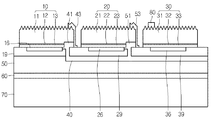
図1は、本発明の一実施例による発光素子を示した図面である。   FIG. 1 illustrates a light emitting device according to an embodiment of the present invention.

本発明の一実施例による発光素子は、図1に示されるように、第1発光構造物10、第2発光構造物20、第3発光構造物30、第1反射電極17、第2反射電極27、第3反射電極37、電極80を備えることができる。図1には、3個の発光構造物が配置された場合を示したが、別の実施例による発光素子は、2個の発光構造物を含むこともできて、また4個以上の発光構造物を含むこともできる。これら複数の発光構造物は電気的に連結されることができる。例えば、これら複数の発光構造物は電気的に直列構造で連結されることができる。第1発光構造物10と第2発光構造物20は、第1コンタクト部43によって電気的に連結することができる。第2発光構造物20と第3発光構造物30は、第2コンタクト部53によって電気的に連結することができる。複数の発光構造物は、支持基板70上に配置することができる。   As shown in FIG. 1, the light emitting device according to an embodiment of the present invention includes a first light emitting structure 10, a second light emitting structure 20, a third light emitting structure 30, a first reflective electrode 17, and a second reflective electrode. 27, a third reflective electrode 37, and an electrode 80 can be provided. Although FIG. 1 illustrates a case where three light emitting structures are arranged, a light emitting device according to another embodiment may include two light emitting structures, and may include four or more light emitting structures. Things can also be included. The plurality of light emitting structures can be electrically connected. For example, the plurality of light emitting structures can be electrically connected in a series structure. The first light emitting structure 10 and the second light emitting structure 20 can be electrically connected by the first contact part 43. The second light emitting structure 20 and the third light emitting structure 30 can be electrically connected by the second contact portion 53. The plurality of light emitting structures can be disposed on the support substrate 70.

第1発光構造物10は、第1導電型の第1半導体層11、第1活性層12、第2導電型の第2半導体層13を有することができる。第1活性層12は第1導電型の第1半導体層11と第2導電型の第2半導体層13との間に配置することができる。第1活性層12は、第1導電型の第1半導体層11の下に配置することができるし、第2導電型の第2半導体層13は、第1活性層12の下に配置することができる。   The first light emitting structure 10 may include a first conductive type first semiconductor layer 11, a first active layer 12, and a second conductive type second semiconductor layer 13. The first active layer 12 may be disposed between the first conductive type first semiconductor layer 11 and the second conductive type second semiconductor layer 13. The first active layer 12 may be disposed under the first conductive type first semiconductor layer 11, and the second conductive type second semiconductor layer 13 may be disposed under the first active layer 12. Can do.

例として、第1導電型の第1半導体層11が第1導電型ドーパントとしてn型ドーパントが添加されたn型半導体層で形成されて、第2導電型の第2半導体層13が第2導電型ドーパントとしてp型ドーパントが添加されたp型半導体層で形成されることができる。また、第1導電型の第1半導体層11がp型半導体層で形成されて、前記第2導電型の第2半導体層13がn型半導体層で形成されることもできる。   As an example, the first conductivity type first semiconductor layer 11 is formed of an n type semiconductor layer to which an n type dopant is added as a first conductivity type dopant, and the second conductivity type second semiconductor layer 13 is a second conductivity type. It can be formed of a p-type semiconductor layer to which a p-type dopant is added as a type dopant. In addition, the first conductive type first semiconductor layer 11 may be formed of a p-type semiconductor layer, and the second conductive type second semiconductor layer 13 may be formed of an n-type semiconductor layer.

第1導電型の第1半導体層11は、例えば、n型半導体層を含むことができる。第1導電型の第1半導体層11は、InAlGa1-x-yN(0≦x≦1、0≦y≦1、0≦x+y≦1)の組成式を有する半導体材料で具現されることができる。第1導電型の第1半導体層11は、例えばGaN、AlN、AlGaN、InGaN、InN、InAlGaN、AlInN、AlGaAs、GaP、GaAs、GaAsP、AlGaInPなどで選択されることができるし、Si、Ge、Sn、Se、Teなどのn型ドーパントがドーピングされることができる。 The first conductivity type first semiconductor layer 11 may include, for example, an n-type semiconductor layer. The first conductivity type first semiconductor layer 11 is a semiconductor material having a composition formula of In x Al y Ga 1-xy N (0 ≦ x ≦ 1, 0 ≦ y ≦ 1, 0 ≦ x + y ≦ 1). Can be implemented. The first conductivity type first semiconductor layer 11 may be selected from, for example, GaN, AlN, AlGaN, InGaN, InN, InAlGaN, AlInN, AlGaAs, GaP, GaAs, GaAsP, AlGaInP, etc., and Si, Ge, An n-type dopant such as Sn, Se, or Te can be doped.

第1活性層12は、第1導電型の第1半導体層11を通じて注入される電子(または、正孔)と第2導電型の第2半導体層13を通じて注入される正孔(または、電子)がお互いに会って、第1活性層12の形成物質によるエネルギーバンド(energy band)のバンドギャップ(band gap)差によって光を放出する層である。第1活性層12は、単一量子井構造、多重量子井構造(MQW:Multi Quantum Well)、量子点構造または量子線構造のうちの何れか一つで形成することができるが、これに限定されるものではない。   The first active layer 12 includes electrons (or holes) injected through the first conductive type first semiconductor layer 11 and holes (or electrons) injected through the second conductive type second semiconductor layer 13. Are layers that emit light due to a band gap difference of energy bands due to a material forming the first active layer 12. The first active layer 12 may be formed of any one of a single quantum well structure, a multiple quantum well (MQW) structure, a quantum dot structure, or a quantum wire structure, but is not limited thereto. Is not to be done.

第1活性層12は、例としてInAlGa1-x-yN(0≦x≦1、0≦y≦1、0≦x+y≦1)の組成式を有する半導体材料で具現されることができる。第1活性層12が前多重量子井構造で具現された場合、第1活性層12は複数の井戸層と複数の障壁層が積層されて具現されることができるし、例えば、InGaN井戸層/GaN障壁層の周期で具現されることができる。 The first active layer 12 is implemented by a semiconductor material having a composition formula of In x Al y Ga 1-xy N (0 ≦ x ≦ 1, 0 ≦ y ≦ 1, 0 ≦ x + y ≦ 1) as an example. be able to. When the first active layer 12 is implemented with a pre-multi-quantum well structure, the first active layer 12 may be implemented by stacking a plurality of well layers and a plurality of barrier layers, for example, an InGaN well layer / It can be implemented with a period of the GaN barrier layer.

第2導電型の第2半導体層13は、例えば、p型半導体層で具現されることができる。第2導電型の第2半導体層13は、InAlGa1-x-yN(0≦x≦1、0≦y≦1、0≦x+y≦1)の組成式を有する半導体材料で具現されることができる。第2導電型の第2半導体層13は、例えばGaN、AlN、AlGaN、InGaN、InN、InAlGaN、AlInN、AlGaAs、GaP、GaAs、GaAsP、AlGaInPなどから選択することができるし、Mg、Zn、Ca、Sr、Baなどのp型ドーパントがドーピングされることができる。 The second conductive type second semiconductor layer 13 may be implemented by a p-type semiconductor layer, for example. The second conductivity type second semiconductor layer 13 is a semiconductor material having a composition formula of In x Al y Ga 1-xy N (0 ≦ x ≦ 1, 0 ≦ y ≦ 1, 0 ≦ x + y ≦ 1). Can be implemented. The second conductive type second semiconductor layer 13 can be selected from, for example, GaN, AlN, AlGaN, InGaN, InN, InAlGaN, AlInN, AlGaAs, GaP, GaAs, GaAsP, AlGaInP, etc., and Mg, Zn, Ca P-type dopants such as Sr, Ba, etc. may be doped.

一方、第1導電型の第1半導体層11がp型半導体層を含んで第2導電型の第2半導体層13がn型半導体層を含むこともできる。また、第2導電型の第2半導体層13の下にはn型またはp型半導体層を含む半導体層がさらに形成されることもできる。これによって、第1発光構造物10はnp、pn、npn、pnp接合構造のうちの少なくとも何れか一つを有することができる。また、第1導電型の第1半導体層11及び第2導電型の第2半導体層13内の不純物のドーピング濃度は、均一または不均一に形成することができる。すなわち、第1発光構造物10の構造は多様に形成することができるし、これに限定しない。   On the other hand, the first conductive type first semiconductor layer 11 may include a p-type semiconductor layer, and the second conductive type second semiconductor layer 13 may include an n-type semiconductor layer. In addition, a semiconductor layer including an n-type or p-type semiconductor layer may be further formed under the second conductive type second semiconductor layer 13. Accordingly, the first light emitting structure 10 may have at least one of np, pn, npn, and pnp junction structures. Further, the doping concentration of impurities in the first conductive type first semiconductor layer 11 and the second conductive type second semiconductor layer 13 can be formed uniformly or non-uniformly. That is, the structure of the first light emitting structure 10 can be variously formed and is not limited thereto.

また、第1導電型の第1半導体層11と第1活性層12との間には第1導電型InGaN/GaNスーパーラティス構造またはInGaN/InGaNスーパーラティス構造が形成されることもできる。また、第2導電型の第2半導体層13と第1活性層12との間には第2導電型のAlGaN層が形成されることもできる。   In addition, a first conductivity type InGaN / GaN super lattice structure or an InGaN / InGaN super lattice structure may be formed between the first conductivity type first semiconductor layer 11 and the first active layer 12. A second conductivity type AlGaN layer may be formed between the second conductivity type second semiconductor layer 13 and the first active layer 12.

そして、第2発光構造物20は、第1導電型の第3半導体層21、第2活性層22、第2導電型の第4半導体層23を有することができる。第2活性層22は、第1導電型の第3半導体層21と第2導電型の第4半導体層23との間に配置することができる。第2活性層22は第1導電型の第3半導体層21の下に配置することができるし、第2導電型の第4半導体層23は第2活性層22の下に配置することができる。第2発光構造物20は上で説明された第1発光構造物10に準じて類似に形成することができる。   The second light emitting structure 20 may include a first conductive type third semiconductor layer 21, a second active layer 22, and a second conductive type fourth semiconductor layer 23. The second active layer 22 may be disposed between the first conductive type third semiconductor layer 21 and the second conductive type fourth semiconductor layer 23. The second active layer 22 can be disposed under the first conductive type third semiconductor layer 21, and the second conductive type fourth semiconductor layer 23 can be disposed under the second active layer 22. . The second light emitting structure 20 can be similarly formed according to the first light emitting structure 10 described above.

また、第3発光構造物30は、第1導電型の第5半導体層31、第3活性層32、第2導電型の第6半導体層33を有することができる。第3活性層32は、第1導電型の第5半導体層31と第2導電型の第6半導体層33との間に配置することができる。第3活性層32は第1導電型の第5半導体層31の下に配置することができるし、第2導電型の第6半導体層33は第3活性層32の下に配置することができる。第3発光構造物30は上で説明された第1発光構造物10に準じて類似に形成することができる。   The third light emitting structure 30 may include a first conductive type fifth semiconductor layer 31, a third active layer 32, and a second conductive type sixth semiconductor layer 33. The third active layer 32 may be disposed between the first conductive type fifth semiconductor layer 31 and the second conductive type sixth semiconductor layer 33. The third active layer 32 can be disposed under the first conductive type fifth semiconductor layer 31, and the second conductive type sixth semiconductor layer 33 can be disposed under the third active layer 32. . The third light emitting structure 30 can be similarly formed according to the first light emitting structure 10 described above.

第1発光構造物10下に第1オーミック接触層15と第1反射電極17が配置されることができる。第1発光構造物10の下及び第1反射電極17のまわりに第1金属層19が配置されることができる。第1金属層19は第1オーミック接触層15のまわり及び第1反射電極17の下に配置することができる。   A first ohmic contact layer 15 and a first reflective electrode 17 may be disposed under the first light emitting structure 10. A first metal layer 19 may be disposed under the first light emitting structure 10 and around the first reflective electrode 17. The first metal layer 19 may be disposed around the first ohmic contact layer 15 and below the first reflective electrode 17.

第1オーミック接触層15は、例えば、透明導電性酸化膜層で形成することができる。第1オーミック接触層15は、例として、ITO(Indium Tin Oxide)、IZO(Indium Zinc Oxide)、AZO(Aluminum Zinc Oxide)、AGZO(Aluminum Gallium Zinc Oxide)、IZTO(Indium Zinc Tin Oxide)、IAZO(Indium Aluminum Zinc Oxide)、IGZO(Indium Gallium Zinc Oxide)、IGTO(Indium Gallium Tin Oxide)、ATO(Antimony Tin Oxide)、GZO(Gallium Zinc Oxide)、IZON(IZO Nitride)、ZnO、IrOx、RuOx、NiO、Pt、Agのうちから選択された少なくとも一つの物質で形成することができる。   The first ohmic contact layer 15 can be formed of, for example, a transparent conductive oxide film layer. The first ohmic contact layer 15 includes, for example, ITO (Indium Tin Oxide), IZO (Indium Zinc Oxide), AZO (Aluminum Zinc Oxide), AGZO (Aluminum Gallium Zinc Oxide), IZTO (Indium Zinc Tin Oxide), and IAZO ( Indium Aluminum Zinc Oxide), IGZO (Indium Gallium Zinc Oxide), IGTO (Indium Gallium Tin Oxide), ATO (Antimony Tin Oxide), GZO (Gallium Zinc Oxide), IZON (IZO Nitride), ZnO, IrOx, RuOx, NiO, It can be formed of at least one substance selected from Pt and Ag.

第1反射電極17は、高反射率を有する金属材質で形成することができる。例えば、第1反射電極17は、Ag、Ni、Al、Rh、Pd、Ir、Ru、Mg、Zn、Pt、Cu、Au、Hfのうちの少なくとも一つを含む金属または合金で形成することができる。また、第1反射電極17は、金属または合金とITO(Indium-Tin-Oxide)、IZO(Indium-Zinc-Oxide)、IZTO(Indium-Zinc-Tin-Oxide)、IAZO(Indium-Aluminum-Zinc-Oxide)、IGZO(Indium-Gallium-Zinc-Oxide)、IGTO(Indium-Gallium-Tin-Oxide)、AZO(Aluminum-Zinc-Oxide)、ATO(Antimony-Tin-Oxide)などの透光性伝導性物質を利用して多層で形成することができる。例えば、実施例で第1反射電極17はAg、Al、Ag-Pd-Cu合金、またはAg-Cu合金のうちの少なくとも何れか一つを含むことができる。   The first reflective electrode 17 can be formed of a metal material having a high reflectance. For example, the first reflective electrode 17 may be formed of a metal or an alloy containing at least one of Ag, Ni, Al, Rh, Pd, Ir, Ru, Mg, Zn, Pt, Cu, Au, and Hf. it can. The first reflective electrode 17 includes a metal or alloy, ITO (Indium-Tin-Oxide), IZO (Indium-Zinc-Oxide), IZTO (Indium-Zinc-Tin-Oxide), and IAZO (Indium-Aluminum-Zinc-). Oxide), IGZO (Indium-Gallium-Zinc-Oxide), IGTO (Indium-Gallium-Tin-Oxide), AZO (Aluminum-Zinc-Oxide), ATO (Antimony-Tin-Oxide), etc. Can be formed in multiple layers. For example, in the embodiment, the first reflective electrode 17 may include at least one of Ag, Al, Ag—Pd—Cu alloy, and Ag—Cu alloy.

第1オーミック接触層15は、第1発光構造物10とオーミック接触になるように形成することができる。また、第1反射電極17は第1発光構造物10から入射される光を反射させて外部に抽出される光量を増加させる機能を遂行することができる。   The first ohmic contact layer 15 can be formed to be in ohmic contact with the first light emitting structure 10. In addition, the first reflective electrode 17 can perform a function of reflecting the light incident from the first light emitting structure 10 and increasing the amount of light extracted to the outside.

第1金属層19は、ボンディング層60が提供される工程でボンディング層60に含まれた物質が第1反射電極17の方向に拡散することを防止する機能を遂行することができる。第1金属層19はボンディング層60に含まれたスズ(Sn)などの物質が第1反射電極17などに影響を及ぼすことを防止することができる。第1金属層19は、Cu、Ni、Ti-W、W、Pt、V、Fe、Mo、Ti、Crのうちの少なくとも一つを含むことができる。第1金属層19は透明導電性酸化膜層で具現されることもできる。第1金属層19はアイソレーション層またはチャンネル層で指称されることもできる。   The first metal layer 19 may perform a function of preventing a material included in the bonding layer 60 from diffusing in the direction of the first reflective electrode 17 in the process of providing the bonding layer 60. The first metal layer 19 can prevent a substance such as tin (Sn) contained in the bonding layer 60 from affecting the first reflective electrode 17 and the like. The first metal layer 19 may include at least one of Cu, Ni, Ti—W, W, Pt, V, Fe, Mo, Ti, and Cr. The first metal layer 19 may be implemented with a transparent conductive oxide film layer. The first metal layer 19 can also be referred to as an isolation layer or a channel layer.

また、第2発光構造物20下に第2オーミック接触層25と第2反射電極27が配置されることができる。第2発光構造物20の下及び第2反射電極27のまわりに第2金属層29が配置されることができる。第2金属層29は、第2オーミック接触層25のまわり及び第2反射電極27の下に配置することができる。   In addition, the second ohmic contact layer 25 and the second reflective electrode 27 may be disposed under the second light emitting structure 20. A second metal layer 29 may be disposed under the second light emitting structure 20 and around the second reflective electrode 27. The second metal layer 29 can be disposed around the second ohmic contact layer 25 and under the second reflective electrode 27.

第2オーミック接触層25は、例えば、透明導電性酸化膜層で形成することができる。第2オーミック接触層25は、例としてITO(Indium Tin Oxide)、IZO(Indium Zinc Oxide)、AZO(Aluminum Zinc Oxide)、AGZO(Aluminum Gallium Zinc Oxide)、IZTO(Indium Zinc Tin Oxide)、IAZO(Indium Aluminum Zinc Oxide)、IGZO(Indium Gallium Zinc Oxide)、IGTO(Indium Gallium Tin Oxide)、ATO(Antimony Tin Oxide)、GZO(Gallium Zinc Oxide)、IZON(IZO Nitride)、ZnO、IrOx、RuOx、NiO、Pt、Agのうちから選択された少なくとも一つの物質で形成することができる。   The second ohmic contact layer 25 can be formed of, for example, a transparent conductive oxide film layer. The second ohmic contact layer 25 includes, for example, ITO (Indium Tin Oxide), IZO (Indium Zinc Oxide), AZO (Aluminum Zinc Oxide), AGZO (Aluminum Gallium Zinc Oxide), IZTO (Indium Zinc Tin Oxide), and IAZO (Indium). Aluminum Zinc Oxide), IGZO (Indium Gallium Zinc Oxide), IGTO (Indium Gallium Tin Oxide), ATO (Antimony Tin Oxide), GZO (Gallium Zinc Oxide), IZON (IZO Nitride), ZnO, IrOx, RuOx, NiO, Pt , Ag, and at least one substance selected from Ag.

第2反射電極27は高反射率を有する金属材質で形成することができる。例えば、第2反射電極27は、Ag、Ni、Al、Rh、Pd、Ir、Ru、Mg、Zn、Pt、Cu、Au、Hfのうちの少なくとも一つを含む金属または合金で形成することができる。また、第2反射電極27は、金属または合金とITO(Indium-Tin-Oxide)、IZO(Indium-Zinc-Oxide)、IZTO(Indium-Zinc-Tin-Oxide)、IAZO(Indium-Aluminum-Zinc-Oxide)、IGZO(Indium-Gallium-Zinc-Oxide)、IGTO(Indium-Gallium-Tin-Oxide)、AZO(Aluminum-Zinc-Oxide)、ATO(Antimony-Tin-Oxide)などの透光性伝導性物質を利用して多層で形成することができる。例えば、実施例で第2反射電極27はAg、Al、Ag-Pd-Cu合金、またはAg-Cu合金のうちの少なくとも何れか一つを含むことができる。   The second reflective electrode 27 can be formed of a metal material having a high reflectance. For example, the second reflective electrode 27 may be formed of a metal or alloy containing at least one of Ag, Ni, Al, Rh, Pd, Ir, Ru, Mg, Zn, Pt, Cu, Au, and Hf. it can. The second reflective electrode 27 includes a metal or an alloy and ITO (Indium-Tin-Oxide), IZO (Indium-Zinc-Oxide), IZTO (Indium-Zinc-Tin-Oxide), and IAZO (Indium-Aluminum-Zinc-). Oxide), IGZO (Indium-Gallium-Zinc-Oxide), IGTO (Indium-Gallium-Tin-Oxide), AZO (Aluminum-Zinc-Oxide), ATO (Antimony-Tin-Oxide), etc. Can be formed in multiple layers. For example, in the embodiment, the second reflective electrode 27 may include at least one of Ag, Al, Ag—Pd—Cu alloy, and Ag—Cu alloy.

第2オーミック接触層25は第2発光構造物20とオーミック接触になるように形成することができる。また、第2反射電極27は第2発光構造物20から入射される光を反射させて外部に抽出される光量を増加させる機能を遂行することができる。   The second ohmic contact layer 25 may be formed to be in ohmic contact with the second light emitting structure 20. In addition, the second reflective electrode 27 can perform a function of reflecting the light incident from the second light emitting structure 20 and increasing the amount of light extracted to the outside.

第2金属層29はボンディング層60が提供される工程でボンディング層60に含まれた物質が第2反射電極27の方向に拡散することを防止する機能を遂行することができる。第2金属層29はボンディング層60に含まれたスズ(Sn)などの物質が第2反射電極27などに影響を及ぼすことを防止することができる。第2金属層29は、Cu、Ni、Ti-W、W、Pt、V、Fe、Mo、Ti、Crのうちの少なくとも一つを含むことができる。第2金属層29は透明導電性酸化膜層で具現されることもできる。   The second metal layer 29 may perform a function of preventing a material included in the bonding layer 60 from diffusing in the direction of the second reflective electrode 27 in the process of providing the bonding layer 60. The second metal layer 29 can prevent a substance such as tin (Sn) contained in the bonding layer 60 from affecting the second reflective electrode 27 and the like. The second metal layer 29 may include at least one of Cu, Ni, Ti—W, W, Pt, V, Fe, Mo, Ti, and Cr. The second metal layer 29 may be implemented with a transparent conductive oxide film layer.

また、第3発光構造物30下に第3オーミック接触層35と第3反射電極37が配置されることができる。第3発光構造物30の下及び第3反射電極37のまわりに第3金属層39が配置されることができる。第3金属層39は第3オーミック接触層35のまわり及び第3反射電極37の下に配置することができる。   In addition, the third ohmic contact layer 35 and the third reflective electrode 37 may be disposed under the third light emitting structure 30. A third metal layer 39 may be disposed under the third light emitting structure 30 and around the third reflective electrode 37. The third metal layer 39 may be disposed around the third ohmic contact layer 35 and below the third reflective electrode 37.

第3オーミック接触層35は、例えば、透明導電性酸化膜層で形成することができる。第3オーミック接触層35は、例としてITO(Indium Tin Oxide)、IZO(Indium Zinc Oxide)、AZO(Aluminum Zinc Oxide)、AGZO(Aluminum Gallium Zinc Oxide)、IZTO(Indium Zinc Tin Oxide)、IAZO(Indium Aluminum Zinc Oxide)、IGZO(Indium Gallium Zinc Oxide)、IGTO(Indium Gallium Tin Oxide)、ATO(Antimony Tin Oxide)、GZO(Gallium Zinc Oxide)、IZON(IZO Nitride)、ZnO、IrOx、RuOx、NiO、Pt、Agのうちから選択された少なくとも一つの物質で形成することができる。   The third ohmic contact layer 35 can be formed of, for example, a transparent conductive oxide film layer. The third ohmic contact layer 35 includes, for example, ITO (Indium Tin Oxide), IZO (Indium Zinc Oxide), AZO (Aluminum Zinc Oxide), AGZO (Aluminum Gallium Zinc Oxide), IZTO (Indium Zinc Tin Oxide), and IAZO (Indium). Aluminum Zinc Oxide), IGZO (Indium Gallium Zinc Oxide), IGTO (Indium Gallium Tin Oxide), ATO (Antimony Tin Oxide), GZO (Gallium Zinc Oxide), IZON (IZO Nitride), ZnO, IrOx, RuOx, NiO, Pt , Ag, and at least one substance selected from Ag.

第3反射電極37は高反射率を有する金属材質で形成することができる。例えば、第3反射電極37は、Ag、Ni、Al、Rh、Pd、Ir、Ru、Mg、Zn、Pt、Cu、Au、Hfのうちの少なくとも一つを含む金属または合金で形成することができる。また、第3反射電極37は、金属または合金とITO(Indium-Tin-Oxide)、IZO(Indium-Zinc-Oxide)、IZTO(Indium-Zinc-Tin-Oxide)、IAZO(Indium-Aluminum-Zinc-Oxide)、IGZO(Indium-Gallium-Zinc-Oxide)、IGTO(Indium-Gallium-Tin-Oxide)、AZO(Aluminum-Zinc-Oxide)、ATO(Antimony-Tin-Oxide)などの透光性伝導性物質を利用して多層で形成することができる。例えば、実施例で第3反射電極37はAg、Al、Ag-Pd-Cu合金、またはAg-Cu合金のうちの少なくとも何れか一つを含むことができる。   The third reflective electrode 37 can be formed of a metal material having a high reflectance. For example, the third reflective electrode 37 may be formed of a metal or alloy containing at least one of Ag, Ni, Al, Rh, Pd, Ir, Ru, Mg, Zn, Pt, Cu, Au, and Hf. it can. The third reflective electrode 37 includes a metal or alloy and ITO (Indium-Tin-Oxide), IZO (Indium-Zinc-Oxide), IZTO (Indium-Zinc-Tin-Oxide), and IAZO (Indium-Aluminum-Zinc-). Oxide), IGZO (Indium-Gallium-Zinc-Oxide), IGTO (Indium-Gallium-Tin-Oxide), AZO (Aluminum-Zinc-Oxide), ATO (Antimony-Tin-Oxide), etc. Can be formed in multiple layers. For example, in the embodiment, the third reflective electrode 37 may include at least one of Ag, Al, Ag—Pd—Cu alloy, and Ag—Cu alloy.

第3オーミック接触層35は第3発光構造物30とオーミック接触になるように形成することができる。また、第3反射電極37は第3発光構造物30から入射される光を反射させて外部に抽出される光量を増加させる機能を遂行することができる。   The third ohmic contact layer 35 can be formed to be in ohmic contact with the third light emitting structure 30. In addition, the third reflective electrode 37 can perform a function of reflecting the light incident from the third light emitting structure 30 and increasing the amount of light extracted to the outside.

第3金属層39はボンディング層60が提供される工程でボンディング層60に含まれた物質が第3反射電極37の方向に拡散することを防止する機能を遂行することができる。第3金属層39はボンディング層60に含まれたスズ(Sn)などの物質が第3反射電極37などに影響を及ぼすことを防止することができる。第3金属層39は、Cu、Ni、Ti-W、W、Pt、V、Fe、Mo、Ti、Crのうちの少なくとも一つを含むことができる。   The third metal layer 39 may perform a function of preventing a material included in the bonding layer 60 from diffusing in the direction of the third reflective electrode 37 in the process of providing the bonding layer 60. The third metal layer 39 can prevent a substance such as tin (Sn) contained in the bonding layer 60 from affecting the third reflective electrode 37 and the like. The third metal layer 39 may include at least one of Cu, Ni, Ti—W, W, Pt, V, Fe, Mo, Ti, and Cr.

第1発光構造物10と第2発光構造物20との間に第1コンタクト部43が配置されることができる。第1コンタクト部43は第1導電型の第1半導体層11の上部面に接触することができる。第1コンタクト部43は第1導電型の第1半導体層11の側面に接触することができる。第1コンタクト部43は第2金属層29に接触することができる。第1コンタクト部43は第2金属層29の上部面に接触することができる。第2金属層29は、第2反射電極27及び第2オーミック接触層25と電気的に連結されるので、第1コンタクト部43は第2導電型の第4半導体層23に電気的に連結されることができる。これによって、第1導電型の第1半導体層11は第1コンタクト部43を通じて第2導電型の第4半導体層23に電気的に連結されることができる。   The first contact part 43 may be disposed between the first light emitting structure 10 and the second light emitting structure 20. The first contact portion 43 can contact the upper surface of the first conductive type first semiconductor layer 11. The first contact portion 43 can contact the side surface of the first conductive type first semiconductor layer 11. The first contact part 43 can contact the second metal layer 29. The first contact part 43 can contact the upper surface of the second metal layer 29. Since the second metal layer 29 is electrically connected to the second reflective electrode 27 and the second ohmic contact layer 25, the first contact part 43 is electrically connected to the second conductive type fourth semiconductor layer 23. Can. Accordingly, the first conductive type first semiconductor layer 11 can be electrically connected to the second conductive type fourth semiconductor layer 23 through the first contact portion 43.

第1コンタクト部43は、例えばCr、Al、Ti、Ni、Pt、V、Agのうちから選択された少なくとも一つの物質で具現されることができる。また、第1コンタクト部43は、例えば、透明導電性酸化膜層で形成されることができる。第1コンタクト部43は、例としてITO(Indium Tin Oxide)、IZO(Indium Zinc Oxide)、AZO(Aluminum Zinc Oxide)、AGZO(Aluminum Gallium Zinc Oxide)、IZTO(Indium Zinc Tin Oxide)、IAZO(Indium Aluminum Zinc Oxide)、IGZO(Indium Gallium Zinc Oxide)、IGTO(Indium Gallium Tin Oxide)、ATO(Antimony Tin Oxide)、GZO(Gallium Zinc Oxide)、IZON(IZO Nitride)、ZnO、IrOx、RuOx、NiOのうちから選択された少なくとも一つの物質で形成されることができる。   The first contact part 43 may be implemented by at least one material selected from, for example, Cr, Al, Ti, Ni, Pt, V, and Ag. The first contact portion 43 can be formed of, for example, a transparent conductive oxide film layer. The first contact portion 43 includes, for example, ITO (Indium Tin Oxide), IZO (Indium Zinc Oxide), AZO (Aluminum Zinc Oxide), AGZO (Aluminum Gallium Zinc Oxide), IZTO (Indium Zinc Tin Oxide), and IAZO (Indium Aluminum). Zinc Oxide), IGZO (Indium Gallium Zinc Oxide), IGTO (Indium Gallium Tin Oxide), ATO (Antimony Tin Oxide), GZO (Gallium Zinc Oxide), IZON (IZO Nitride), ZnO, IrOx, RuOx, NiO It can be formed of at least one selected material.

第1コンタクト部43は、第1導電型の第1半導体層11上部面に接触することができる。例えば、第1導電型の第1半導体層11がGaN層を含んで具現されることができる。このとき、半導体層の成長方向及び蝕刻方向を考慮すれば、第1コンタクト部43は第1導電型の第1半導体層11のN面(N face)に接触することができる。   The first contact portion 43 can contact the upper surface of the first conductive type first semiconductor layer 11. For example, the first conductive type first semiconductor layer 11 may be implemented to include a GaN layer. At this time, in consideration of the growth direction and the etching direction of the semiconductor layer, the first contact portion 43 can contact the N face of the first conductive type first semiconductor layer 11.

第1コンタクト部43と第2導電型の第2半導体層13との間に第1絶縁層41が配置されることができる。第1コンタクト部43と第1活性層12との間に第1絶縁層41が配置されることができる。第1絶縁層41は第1導電型の第1半導体層11下部に配置することができる。第1絶縁層41は第1コンタクト部43に接触して配置することができる。第1絶縁層41の側面は第1コンタクト部43に接触して配置することができる。第1絶縁層41は透光性または絶縁性物質で具現されることができる。第1絶縁層41は、例えば、SiO2、SiO、SiO、Si34、Al23、TiO2、AlNのような材質で形成することができる。 The first insulating layer 41 may be disposed between the first contact part 43 and the second conductive type second semiconductor layer 13. A first insulating layer 41 may be disposed between the first contact part 43 and the first active layer 12. The first insulating layer 41 can be disposed under the first conductive type first semiconductor layer 11. The first insulating layer 41 can be disposed in contact with the first contact portion 43. The side surface of the first insulating layer 41 can be disposed in contact with the first contact portion 43. The first insulating layer 41 may be implemented with a light transmitting or insulating material. The first insulating layer 41 may be formed of SiO 2, SiO x, a material such as SiO x N y, Si 3 N 4, Al 2 O 3, TiO 2, AlN.

第2発光構造物20と第3発光構造物30との間に第2コンタクト部53が配置されることができる。第2コンタクト部53は、第1導電型の第3半導体層21の上部面に接触することができる。第2コンタクト部53は第1導電型の第3半導体層21の側面に接触することができる。第2コンタクト部53は第3金属層39に接触することができる。第2コンタクト部53は第3金属層39の上部面に接触することができる。第3金属層39は第3反射電極37及び第3オーミック接触層35と電気的に連結されるので、第2コンタクト部53は第2導電型の第6半導体層33に電気的に連結されることができる。これによって、第1導電型の第3半導体層21は第2コンタクト部53を通じて第2導電型の第6半導体層33に電気的に連結されることができる。   The second contact part 53 may be disposed between the second light emitting structure 20 and the third light emitting structure 30. The second contact portion 53 can be in contact with the upper surface of the first conductive type third semiconductor layer 21. The second contact portion 53 can contact the side surface of the first conductive type third semiconductor layer 21. The second contact part 53 can contact the third metal layer 39. The second contact part 53 can contact the upper surface of the third metal layer 39. Since the third metal layer 39 is electrically connected to the third reflective electrode 37 and the third ohmic contact layer 35, the second contact portion 53 is electrically connected to the second conductive type sixth semiconductor layer 33. be able to. Accordingly, the first conductive type third semiconductor layer 21 can be electrically connected to the second conductive type sixth semiconductor layer 33 through the second contact portion 53.

第2コンタクト部53は、例えばCr、Al、Ti、Ni、Pt、V、Agのうちから選択された少なくとも一つの物質で具現されることができる。また、第2コンタクト部53は、例えば、透明導電性酸化膜層で形成することができる。第2コンタクト部53は、例としてITO(Indium Tin Oxide)、IZO(Indium Zinc Oxide)、AZO(Aluminum Zinc Oxide)、AGZO(Aluminum Gallium Zinc Oxide)、IZTO(Indium Zinc Tin Oxide)、IAZO(Indium Aluminum Zinc Oxide)、IGZO(Indium Gallium Zinc Oxide)、IGTO(Indium Gallium Tin Oxide)、ATO(Antimony Tin Oxide)、GZO(Gallium Zinc Oxide)、IZON(IZO Nitride)、ZnO、IrOx、RuOx、NiOのうちから選択された少なくとも一つの物質で形成することができる。   The second contact part 53 may be implemented with at least one material selected from, for example, Cr, Al, Ti, Ni, Pt, V, and Ag. Further, the second contact portion 53 can be formed of, for example, a transparent conductive oxide film layer. The second contact portion 53 includes, for example, ITO (Indium Tin Oxide), IZO (Indium Zinc Oxide), AZO (Aluminum Zinc Oxide), AGZO (Aluminum Gallium Zinc Oxide), IZTO (Indium Zinc Tin Oxide), and IAZO (Indium Aluminum). Zinc Oxide), IGZO (Indium Gallium Zinc Oxide), IGTO (Indium Gallium Tin Oxide), ATO (Antimony Tin Oxide), GZO (Gallium Zinc Oxide), IZON (IZO Nitride), ZnO, IrOx, RuOx, NiO It can be formed of at least one selected material.

第2コンタクト部53は第1導電型の第3半導体層21上部面に接触することができる。例えば、第1導電型の第3半導体層21がGaN層を含んで具現されることができる。このとき、半導体層の成長方向及び蝕刻方向を考慮すれば、第2コンタクト部53は第1導電型の第3半導体層21のN面(N face)に接触することができる。   The second contact part 53 can contact the upper surface of the first conductive type third semiconductor layer 21. For example, the third semiconductor layer 21 of the first conductivity type may be implemented including a GaN layer. At this time, if the growth direction and the etching direction of the semiconductor layer are taken into consideration, the second contact portion 53 can contact the N face of the third semiconductor layer 21 of the first conductivity type.

第2コンタクト部53と第2導電型の第4半導体層23との間に第2絶縁層51が配置されることができる。第2コンタクト部53と第2活性層22との間に第2絶縁層51が配置されることができる。第2絶縁層51は、第1導電型の第3半導体層21の下部に配置することができる。第2絶縁層51は、第2コンタクト部53に接触して配置することができる。第2絶縁層51の側面は、第2コンタクト部53に接触して配置することができる。第2絶縁層51は、透光性または絶縁性材質で具現されることができる。第2絶縁層51は、例えば、SiO2、SiO、SiO、Si34、Al23、TiO2、AlNのような物質で形成することができる。 A second insulating layer 51 may be disposed between the second contact portion 53 and the second conductive type fourth semiconductor layer 23. A second insulating layer 51 may be disposed between the second contact part 53 and the second active layer 22. The second insulating layer 51 can be disposed under the first conductive type third semiconductor layer 21. The second insulating layer 51 can be disposed in contact with the second contact portion 53. The side surface of the second insulating layer 51 can be disposed in contact with the second contact portion 53. The second insulating layer 51 may be implemented with a light transmitting or insulating material. The second insulating layer 51 can be formed of a material such as SiO 2 , SiO x , SiO x N y , Si 3 N 4 , Al 2 O 3 , TiO 2 , or AlN.

第2金属層29及び第3金属層39下に第3絶縁層40が配置されることができる。第3絶縁層40は酸化物または窒化物で具現されることができる。第3絶縁層40は、例えば、SiO2、SiO、SiO、Si34、Al23のように透光性及び絶縁性を有する材質で形成することができる。また、第3絶縁層40は、第1絶縁層41下に接触して配置することができる。また、第3絶縁層40は第2絶縁層51下に接触して配置することができる。第3絶縁層40の第1領域は、第1金属層19と第2金属層29との間に配置することができる。第3絶縁層40の第2領域は、第2金属層29と第3金属層39との間に配置することができる。 A third insulating layer 40 may be disposed under the second metal layer 29 and the third metal layer 39. The third insulating layer 40 may be implemented with an oxide or a nitride. The third insulating layer 40 can be formed of a material having translucency and insulating properties such as SiO 2 , SiO x , SiO x N y , Si 3 N 4 , and Al 2 O 3 . Further, the third insulating layer 40 can be disposed in contact with the first insulating layer 41 below. In addition, the third insulating layer 40 can be disposed in contact with the second insulating layer 51. The first region of the third insulating layer 40 can be disposed between the first metal layer 19 and the second metal layer 29. The second region of the third insulating layer 40 can be disposed between the second metal layer 29 and the third metal layer 39.

第1金属層19と第3絶縁層40下に拡散障壁層50、ボンディング層60、支持部材70が配置されることができる。   A diffusion barrier layer 50, a bonding layer 60, and a support member 70 may be disposed under the first metal layer 19 and the third insulating layer 40.

拡散障壁層50はボンディング層60が提供される工程でボンディング層60に含まれた物質が第1反射電極17、第2反射電極27、第3反射電極37の方向に拡散することを防止する機能を遂行することができる。拡散障壁層50はボンディング層60に含まれたスズ(Sn)などの物質が第1反射電極17、第2反射電極27、第3反射電極37などに影響を及ぼすことを防止することができる。拡散障壁層50はCu、Ni、Ti-W、W、Pt、V、Fe、Mo、Tiのうちの少なくとも一つを含むことができる。   The diffusion barrier layer 50 has a function of preventing the material contained in the bonding layer 60 from diffusing in the direction of the first reflective electrode 17, the second reflective electrode 27, and the third reflective electrode 37 in the process of providing the bonding layer 60. Can be carried out. The diffusion barrier layer 50 can prevent substances such as tin (Sn) contained in the bonding layer 60 from affecting the first reflective electrode 17, the second reflective electrode 27, the third reflective electrode 37, and the like. The diffusion barrier layer 50 may include at least one of Cu, Ni, Ti—W, W, Pt, V, Fe, Mo, and Ti.

ボンディング層60はバリア金属またはボンディング金属などを含んで、例えば、Ti、Au、Sn、Ni、Cr、Ga、In、Bi、Cu、Ag、Nb、PdまたはTaのうちの少なくとも一つを含むことができる。支持部材70は実施例による発光素子を支持して、外部電極と電気的に連結されて第1発光構造物10に電源を提供することができる。ボンディング層60はシード層で具現されることもできる。   The bonding layer 60 includes a barrier metal or a bonding metal, and includes, for example, at least one of Ti, Au, Sn, Ni, Cr, Ga, In, Bi, Cu, Ag, Nb, Pd, or Ta. Can do. The support member 70 supports the light emitting device according to the embodiment, and is electrically connected to the external electrode to provide power to the first light emitting structure 10. The bonding layer 60 may be implemented with a seed layer.

支持部材70は、例えば、Ti、Cr、Ni、Al、Pt、Au、W、Cu、Mo、Cu-Wまたは不純物が注入された半導体基板(例:Si、Ge、GaN、GaAs、ZnO、SiC、SiGeなど)のうちの少なくとも何れか一つで形成することができる。また、支持部材70は絶縁性物質で具現されることもできる。支持部材70は、例えばAl23、SiO2などの物質で具現されることもできる。 The support member 70 may be, for example, Ti, Cr, Ni, Al, Pt, Au, W, Cu, Mo, Cu—W, or a semiconductor substrate into which impurities are implanted (eg, Si, Ge, GaN, GaAs, ZnO, SiC). , SiGe, etc.). In addition, the support member 70 may be implemented with an insulating material. The support member 70 may be implemented by a material such as Al 2 O 3 or SiO 2 .

一方、第1導電型の第5半導体層31上に電極80が配置されることができる。電極80は第1導電型の第5半導体層31に電気的に連結されることができる。電極80は第1導電型の第5半導体層31上部面に接触することができる。   Meanwhile, the electrode 80 may be disposed on the first conductive type fifth semiconductor layer 31. The electrode 80 may be electrically connected to the first conductive type fifth semiconductor layer 31. The electrode 80 may be in contact with the upper surface of the first conductive type fifth semiconductor layer 31.

これによって、電極80及び第1反射電極17によって第1発光構造物10、第2発光構造物20、及び第3発光構造物30に電源が提供されることができるようになる。第1発光構造物10、第2発光構造物20、第3発光構造物30は電気的に直列構造で連結される。これによって、電極80及び第1反射電極17を通じて電源が印加されれば第1発光構造物10、第2発光構造物20、第3発光構造物30で光が提供されることができるようになる。   As a result, power can be provided to the first light emitting structure 10, the second light emitting structure 20, and the third light emitting structure 30 by the electrode 80 and the first reflective electrode 17. The first light emitting structure 10, the second light emitting structure 20, and the third light emitting structure 30 are electrically connected in a series structure. Accordingly, when power is applied through the electrode 80 and the first reflective electrode 17, light can be provided by the first light emitting structure 10, the second light emitting structure 20, and the third light emitting structure 30. .

本発明の一実施例によれば、電極80は多層構造で具現されることもできる。電極80はオーミック接触層、中問層、上部層で具現されることができる。オーミック接触層は、Cr、V、W、Ti、Znなどから選択された物質を含んでオーミック接触を具現することができる。中問層はNi、Cu、Alなどから選択された物質で具現されることができる。上部層は、例えばAuを含むことができる。   According to an embodiment of the present invention, the electrode 80 may be implemented with a multilayer structure. The electrode 80 may be implemented with an ohmic contact layer, a middle layer, and an upper layer. The ohmic contact layer may implement an ohmic contact including a material selected from Cr, V, W, Ti, Zn, and the like. The intermediate layer may be implemented with a material selected from Ni, Cu, Al, and the like. The upper layer can include, for example, Au.

第1発光構造物10、第2発光構造物20、第3発光構造物30の上部面に光抽出パターンが提供されることができる。第1発光構造物10、第2発光構造物20、第3発光構造物30の上部面に凹凸パターンが提供されることができる。これによって、本発明の一実施例によれば、外部光抽出効果を上昇させることができるようになる。   A light extraction pattern may be provided on the upper surface of the first light emitting structure 10, the second light emitting structure 20, and the third light emitting structure 30. An uneven pattern may be provided on the upper surface of the first light emitting structure 10, the second light emitting structure 20, and the third light emitting structure 30. Thus, according to an embodiment of the present invention, the external light extraction effect can be increased.

本発明の一実施例によれば、第1発光構造物10、第2発光構造物20、第3発光構造物30の上部面がN面で形成されることができるし、Ga面で形成される場合に比べて表面粗さが大きいので、光抽出効率がさらに向上することができるようになる。また、電極80と第1導電型の第5半導体層31との間にアンドープGaN層がさらに配置されることもできる。これによってN面に接した電極80に対してアンドープGaN層が一種のバランス抵抗役割を遂行することができるようになるし、動作電圧を変動させることができるようになる。   According to an embodiment of the present invention, the upper surfaces of the first light emitting structure 10, the second light emitting structure 20, and the third light emitting structure 30 may be formed with an N plane, and may be formed with a Ga plane. Since the surface roughness is large compared to the case where the light extraction is performed, the light extraction efficiency can be further improved. Further, an undoped GaN layer may be further disposed between the electrode 80 and the first conductivity type fifth semiconductor layer 31. As a result, the undoped GaN layer can perform a kind of balance resistance role with respect to the electrode 80 in contact with the N plane, and the operating voltage can be changed.

第1発光構造物10、第2発光構造物20、第3発光構造物30上には保護層がさらに配置されることができる。保護層は、酸化物または窒化物で具現されることができる。保護層は、例えば、SiO2、SiO、SiO、Si34、Al23のように透光性及び絶縁性を有する材質で形成することができる。保護層は第1発光構造物10及び第3発光構造物30のまわりに提供されることができる。 A protective layer may be further disposed on the first light emitting structure 10, the second light emitting structure 20, and the third light emitting structure 30. The protective layer may be implemented with an oxide or a nitride. The protective layer may be formed of a material having a SiO 2, SiO x, SiO x N y, Si 3 N 4, translucency and insulation so as Al 2 O 3. A protective layer may be provided around the first light emitting structure 10 and the third light emitting structure 30.

本発明の一実施例によれば、第1コンタクト部43及び第2コンタクト部53を通じて隣り合う発光構造物間に電気的に直列構造で連結されることができる。また、第1発光構造物10と第2発光構造物20との間に別途の絶縁層が配置されないことによって、第1コンタクト部43を形成するにおいて絶縁層を蝕刻する工程が必要ではなくなる。これによって第1コンタクト部43を形成するにおいて製造安全性を高めることができるようになる。すなわち、絶縁層を形成するための工程及び絶縁層に対する蝕刻工程を経らなくても良いので、相対的に工程安全性を確保することができるようになる。   According to an embodiment of the present invention, the light emitting structures adjacent to each other can be electrically connected in a series structure through the first contact part 43 and the second contact part 53. In addition, since a separate insulating layer is not disposed between the first light emitting structure 10 and the second light emitting structure 20, a step of etching the insulating layer in forming the first contact portion 43 is not necessary. This makes it possible to improve manufacturing safety in forming the first contact portion 43. That is, since it is not necessary to go through the process for forming the insulating layer and the etching process for the insulating layer, process safety can be relatively ensured.

本発明の一実施例による発光素子は、複数の発光セルを含む。それぞれの発光セルは、反射電極、反射電極上の第2導電型半導体層、第2導電型半導体層の上の活性層、活性層の上の第1導電型半導体層を有することができる。また、複数の発光セルのうちで第1発光セルの第1導電型半導体層の側面に接触して、第1発光セルに隣接した第2発光セルの反射電極を電気的に連結するコンタクト部を備える。このとき、コンタクト部は第1発光セルの第1導電型半導体層の上部面に接触して第2発光セルの反射電極に電気的に連結されることができる。コンタクト部と第1発光セルの活性層との間及びコンタクト部と第1発光セルの第2導電型半導体層との間に絶縁層が配置されることができる。当該絶縁層は、第1発光セルの第1導電型半導体層の下部に配置することができる。そして、第2発光セルの第1導電型半導体層に電気的に連結された電極を備えることができる。これによって第1発光セルに含まれた反射電極と第2発光セルに含まれた電極に電源が提供されれば第1発光セルと第2発光セルは電気的に直列構造で連結されて光を発光することができるようになる。   A light emitting device according to an embodiment of the present invention includes a plurality of light emitting cells. Each light emitting cell may have a reflective electrode, a second conductive semiconductor layer on the reflective electrode, an active layer on the second conductive semiconductor layer, and a first conductive semiconductor layer on the active layer. Further, a contact portion that contacts a side surface of the first conductive type semiconductor layer of the first light emitting cell among the plurality of light emitting cells and electrically connects the reflective electrode of the second light emitting cell adjacent to the first light emitting cell is provided. Prepare. At this time, the contact portion may be in contact with the upper surface of the first conductive semiconductor layer of the first light emitting cell and electrically connected to the reflective electrode of the second light emitting cell. An insulating layer may be disposed between the contact portion and the active layer of the first light emitting cell and between the contact portion and the second conductive semiconductor layer of the first light emitting cell. The insulating layer can be disposed under the first conductive semiconductor layer of the first light emitting cell. An electrode electrically connected to the first conductivity type semiconductor layer of the second light emitting cell may be provided. Accordingly, if power is provided to the reflective electrode included in the first light emitting cell and the electrode included in the second light emitting cell, the first light emitting cell and the second light emitting cell are electrically connected in a series structure to transmit light. It becomes possible to emit light.

そうすると、図2乃至図6を参照して、本発明の一実施例による発光素子製造方法を説明することにする。   Then, a method for manufacturing a light emitting device according to an embodiment of the present invention will be described with reference to FIGS.

本発明の一実施例による発光素子製造方法によれば、図2に示されるように、成長基板5上に、第1導電型半導体層11a、活性層12a、第2導電型半導体層13aを形成する。第1導電型半導体層11a、前記活性層12a、第2導電型半導体層13aは、発光構造物10aで定義されることができる。   According to the light emitting device manufacturing method according to an embodiment of the present invention, as shown in FIG. 2, the first conductive semiconductor layer 11a, the active layer 12a, and the second conductive semiconductor layer 13a are formed on the growth substrate 5. To do. The first conductive semiconductor layer 11a, the active layer 12a, and the second conductive semiconductor layer 13a may be defined by a light emitting structure 10a.

成長基板5は、例えば、サファイア基板(Al2)、SiC、GaAs、GaN、ZnO、Si、GaP、InP、Geのうちの少なくとも一つで形成することができるし、これに限定しない。第1導電型の第1半導体層11と前記成長基板5との間にはバッファ層がさらに形成されることができる。 The growth substrate 5 can be formed of, for example, at least one of a sapphire substrate (Al 2 O 3 ), SiC, GaAs, GaN, ZnO, Si, GaP, InP, and Ge, but is not limited thereto. A buffer layer may be further formed between the first conductive type first semiconductor layer 11 and the growth substrate 5.

例として、第1導電型半導体層11aが第1導電型ドーパントとしてn型ドーパントが添加されたn型半導体層で形成されて、第2導電型半導体層13aが第2導電型ドーパントとしてp型ドーパントが添加されたp型半導体層で形成されることができる。また、第1導電型半導体層11aがp型半導体層で形成されて、第2導電型半導体層13aがn型半導体層で形成されることもできる。   For example, the first conductive semiconductor layer 11a is formed of an n-type semiconductor layer to which an n-type dopant is added as a first conductive dopant, and the second conductive semiconductor layer 13a is a p-type dopant as a second conductive dopant. Can be formed of a p-type semiconductor layer to which is added. Alternatively, the first conductive semiconductor layer 11a may be formed of a p-type semiconductor layer, and the second conductive semiconductor layer 13a may be formed of an n-type semiconductor layer.

第1導電型半導体層11aは、例えば、n型半導体層を含むことができる。第1導電型半導体層11aは、InAlGa1-x-yN(0≦x≦1、0≦y≦1、0≦x+y≦1)の組成式を有する半導体材料で形成することができる。第1導電型半導体層11aは、例えばInAlGaN、GaN、AlGaN、AlInN、InGaN、AlN、InNなどから選択することができるし、Si、Ge、Sn、Se、Teなどのn型ドーパントがドーピングされることができる。 The first conductivity type semiconductor layer 11a can include, for example, an n-type semiconductor layer. The first conductivity type semiconductor layer 11a is formed of a semiconductor material having a composition formula of In x Al y Ga 1-xy N (0 ≦ x ≦ 1, 0 ≦ y ≦ 1, 0 ≦ x + y ≦ 1). Can do. The first conductivity type semiconductor layer 11a can be selected from, for example, InAlGaN, GaN, AlGaN, AlInN, InGaN, AlN, InN, etc., and is doped with an n-type dopant such as Si, Ge, Sn, Se, Te. be able to.

活性層12aは第1導電型半導体層11aを通じて注入される電子(または正孔)と第2導電型の半導体層13aを通じて注入される正孔(または電子)がお互いに会って、活性層12aの形成物質によるエネルギーバンド(energy band)のバンドギャップ(band gap)差によって光を放出する層である。活性層12aは単一量子井構造、多重量子井構造(MQW:Multi Quantum Well)、量子点構造または量子線構造のうちの何れか一つで形成することができるが、これに限定されるものではない。   In the active layer 12a, electrons (or holes) injected through the first conductive type semiconductor layer 11a and holes (or electrons) injected through the second conductive type semiconductor layer 13a meet each other, and the active layer 12a It is a layer that emits light due to the band gap difference of the energy band due to the forming material. The active layer 12a may be formed of any one of a single quantum well structure, a multiple quantum well (MQW) structure, a quantum dot structure, or a quantum wire structure, but is not limited thereto. is not.

活性層12aはInAlGa1-x-yN(0≦x≦1、0≦y≦1、0≦x+y≦1)の組成式を有する半導体材料で形成することができる。活性層12aが多重量子井構造で形成された場合、活性層12aは複数の井戸層と複数の障壁層が積層されて形成されることができるし、例えば、InGaN井戸層/GaN障壁層の周期で形成されることができる。 The active layer 12a may be formed of a semiconductor material having a In x Al y Ga 1-xy N (0 ≦ x ≦ 1,0 ≦ y ≦ 1,0 ≦ x + y ≦ 1) of the formula. When the active layer 12a is formed with a multiple quantum well structure, the active layer 12a can be formed by laminating a plurality of well layers and a plurality of barrier layers. For example, the period of the InGaN well layer / GaN barrier layer Can be formed.

第2導電型半導体層13aは、例えば、p型半導体層で具現されることができる。第2導電型半導体層13aはInAlGa1-x-yN(0≦x≦1、0≦y≦1、0≦x+y≦1)の組成式を有する半導体材料で形成することができる。第2導電型半導体層13aは、例えばInAlGaN、GaN、AlGaN、InGaN、AlInN、AlN、InNなどから選択することができるし、Mg、Zn、Ca、Sr、Baなどのp型ドーパントがドーピングされることができる。 For example, the second conductive semiconductor layer 13a may be implemented by a p-type semiconductor layer. The second conductivity type semiconductor layer 13a may be formed of a semiconductor material having a composition formula of In x Al y Ga 1-xy N (0 ≦ x ≦ 1, 0 ≦ y ≦ 1, 0 ≦ x + y ≦ 1). it can. The second conductivity type semiconductor layer 13a can be selected from, for example, InAlGaN, GaN, AlGaN, InGaN, AlInN, AlN, InN, or the like, and is doped with a p-type dopant such as Mg, Zn, Ca, Sr, or Ba. be able to.

一方、第1導電型半導体層11aがp型半導体層を含んで、第2導電型半導体層13aがn型半導体層を含むこともできる。また、第2導電型半導体層13a上にはn型またはp型半導体層を含む半導体層がさらに形成されることもでき、これによって、発光構造物10aは、np、pn、npn、pnp接合構造のうちの少なくとも何れか一つを有することができる。また、第1導電型半導体層11a及び第2導電型半導体層13a内の不純物のドーピング濃度は、均一または不均一に形成することができる。すなわち、発光構造物10aの構造は、多様に形成することができるし、これに限定しない。   Meanwhile, the first conductive semiconductor layer 11a may include a p-type semiconductor layer, and the second conductive semiconductor layer 13a may include an n-type semiconductor layer. In addition, a semiconductor layer including an n-type or p-type semiconductor layer may be further formed on the second conductivity type semiconductor layer 13a, whereby the light emitting structure 10a has an np, pn, npn, pnp junction structure. At least one of them. Further, the doping concentration of impurities in the first conductive semiconductor layer 11a and the second conductive semiconductor layer 13a can be formed uniformly or non-uniformly. That is, the structure of the light emitting structure 10a can be variously formed and is not limited thereto.

また、第1導電型半導体層11aと活性層12aとの間には第1導電型InGaN/GaNスーパーラティス構造、または、InGaN/InGaNスーパーラティス構造が形成されることもできる。また、第2導電型半導体層13aと活性層12aとの間には、第2導電型のAlGaN層が形成されることもできる。   Further, a first conductivity type InGaN / GaN super lattice structure or an InGaN / InGaN super lattice structure may be formed between the first conductivity type semiconductor layer 11a and the active layer 12a. Further, a second conductivity type AlGaN layer may be formed between the second conductivity type semiconductor layer 13a and the active layer 12a.

引き継いで、図3に示されるように、第2導電型半導体層13aの第1領域の上に第1オーミック接触層15、第1反射電極17が形成される。また、第2導電型半導体層13aの第2領域の上に第2オーミック接触層25、第2反射電極27が形成されて、第2導電型半導体層13aの第3領域の上に第3オーミック接触層35、第3反射電極37が形成される。   In succession, as shown in FIG. 3, the first ohmic contact layer 15 and the first reflective electrode 17 are formed on the first region of the second conductivity type semiconductor layer 13a. In addition, the second ohmic contact layer 25 and the second reflective electrode 27 are formed on the second region of the second conductive semiconductor layer 13a, and the third ohmic contact is formed on the third region of the second conductive semiconductor layer 13a. A contact layer 35 and a third reflective electrode 37 are formed.

第1オーミック接触層15、第2オーミック接触層25、第3オーミック接触層35は、例えば、透明導電性酸化膜層で形成することができる。第1オーミック接触層15、第2オーミック接触層25、第3オーミック接触層35は、例としてITO(Indium Tin Oxide)、IZO(Indium Zinc Oxide)、AZO(Aluminum Zinc Oxide)、AGZO(Aluminum Gallium Zinc Oxide)、IZTO(Indium Zinc Tin Oxide)、IAZO(Indium Aluminum Zinc Oxide)、IGZO(Indium Gallium Zinc Oxide)、IGTO(Indium Gallium Tin Oxide)、ATO(Antimony Tin Oxide)、GZO(Gallium Zinc Oxide)、IZON(IZO Nitride)、ZnO、IrOx、RuOx、NiO、Pt、Agのうちから選択された少なくとも一つの物質で形成することができる。   The 1st ohmic contact layer 15, the 2nd ohmic contact layer 25, and the 3rd ohmic contact layer 35 can be formed with a transparent conductive oxide film layer, for example. The first ohmic contact layer 15, the second ohmic contact layer 25, and the third ohmic contact layer 35 are, for example, ITO (Indium Tin Oxide), IZO (Indium Zinc Oxide), AZO (Aluminum Zinc Oxide), and AGZO (Aluminum Gallium Zinc). Oxide), IZTO (Indium Zinc Tin Oxide), IAZO (Indium Aluminum Zinc Oxide), IGZO (Indium Gallium Zinc Oxide), IGTO (Indium Gallium Tin Oxide), ATO (Antimony Tin Oxide), GZO (Gallium Zinc Oxide), IZON It can be formed of at least one material selected from (IZO Nitride), ZnO, IrOx, RuOx, NiO, Pt, and Ag.

第1反射電極17、第2反射電極27、第3反射電極37は高反射率を有する金属材質で形成することができる。例えば、第1反射電極17、第2反射電極27、第3反射電極37は、Ag、Ni、Al、Rh、Pd、Ir、Ru、Mg、Zn、Pt、Cu、Au、Hfのうちの少なくとも一つを含む金属または合金で形成されることができる。また、第1反射電極17、第2反射電極27、第3反射電極37は、金属または合金とITO(Indium-Tin-Oxide)、IZO(Indium-Zinc-Oxide)、IZTO(Indium-Zinc-Tin-Oxide)、IAZO(Indium-Aluminum-Zinc-Oxide)、IGZO(Indium-Gallium-Zinc-Oxide)、IGTO(Indium-Gallium-Tin-Oxide)、AZO(Aluminum-Zinc-Oxide)、ATO(Antimony-Tin-Oxide)などの透光性伝導性物質を利用して多層で形成されることができる。例えば、実施例で第1反射電極17、第2反射電極27、第3反射電極37はAg、Al、Ag-Pd-Cu合金、またはAg-Cu合金のうちの少なくとも何れか一つを含むことができる。   The first reflective electrode 17, the second reflective electrode 27, and the third reflective electrode 37 can be formed of a metal material having a high reflectance. For example, the first reflective electrode 17, the second reflective electrode 27, and the third reflective electrode 37 are made of at least Ag, Ni, Al, Rh, Pd, Ir, Ru, Mg, Zn, Pt, Cu, Au, and Hf. It can be made of one or more metals or alloys. The first reflective electrode 17, the second reflective electrode 27, and the third reflective electrode 37 are made of a metal or an alloy and ITO (Indium-Tin-Oxide), IZO (Indium-Zinc-Oxide), IZTO (Indium-Zinc-Tin). -Oxide), IAZO (Indium-Aluminum-Zinc-Oxide), IGZO (Indium-Gallium-Zinc-Oxide), IGTO (Indium-Gallium-Tin-Oxide), AZO (Aluminum-Zinc-Oxide), ATO (Antimony- It can be formed in multiple layers using a light-transmitting conductive material such as Tin-Oxide. For example, in the embodiment, the first reflective electrode 17, the second reflective electrode 27, and the third reflective electrode 37 include at least one of Ag, Al, an Ag—Pd—Cu alloy, or an Ag—Cu alloy. Can do.

引き継いで、図4に示されるように、第2導電型の第2半導体層13と第2導電型の第4半導体層23との間に第1絶縁層41が形成される。第1絶縁層41は第1活性層12と第2活性層22との間にも形成される。第1絶縁層41の一部領域は第1オーミック接触層15に接触して形成することができる。第1絶縁層41は第1導電型半導体層11a内部に接触して形成することができる。第1絶縁層41は透光性または絶縁性物質で具現されることができる。第1絶縁層41は、例えば、SiO2、SiO、SiO、Si34、Al23、TiO2、AlNのような材質で形成することができる。 In succession, as shown in FIG. 4, the first insulating layer 41 is formed between the second conductive type second semiconductor layer 13 and the second conductive type fourth semiconductor layer 23. The first insulating layer 41 is also formed between the first active layer 12 and the second active layer 22. A partial region of the first insulating layer 41 can be formed in contact with the first ohmic contact layer 15. The first insulating layer 41 can be formed in contact with the inside of the first conductivity type semiconductor layer 11a. The first insulating layer 41 may be implemented with a light transmitting or insulating material. The first insulating layer 41 may be formed of SiO 2, SiO x, a material such as SiO x N y, Si 3 N 4, Al 2 O 3, TiO 2, AlN.

また、第2導電型の第4半導体層23と第2導電型の第6半導体層33との間に第2絶縁層51が形成される。第2絶縁層51は第2活性層22と第3活性層32との間にも形成される。第2絶縁層51の一部領域は第2オーミック接触層25に接触して形成することができる。第2絶縁層51は第1導電型半導体層11a内部に接触して形成することができる。第2絶縁層51は、例えば、SiO2、SiO、SiO、Si34、Al23、TiO2、AlNのような材質で形成することができる。 A second insulating layer 51 is formed between the second conductive type fourth semiconductor layer 23 and the second conductive type sixth semiconductor layer 33. The second insulating layer 51 is also formed between the second active layer 22 and the third active layer 32. A partial region of the second insulating layer 51 can be formed in contact with the second ohmic contact layer 25. The second insulating layer 51 can be formed in contact with the inside of the first conductivity type semiconductor layer 11a. The second insulating layer 51 can be formed of a material such as SiO 2 , SiO x , SiO x N y , Si 3 N 4 , Al 2 O 3 , TiO 2 , or AlN.

引き継いで、図5に示されるように、第1反射電極17、第2反射電極27、第3反射電極37、第1絶縁層41、第2絶縁層51上に金属層を形成して、第3絶縁層40を形成する。第3絶縁層40によって金属層は、第1金属層19、第2金属層29、第3金属層39に分離することができる。第1金属層19、第2金属層29、第3金属層39は第3絶縁層40によって電気的に絶縁されることができる。第3絶縁層40は第1絶縁層41上に接触して形成することができる。第3絶縁層40は第2絶縁層51上に接触して形成することができる。   In succession, as shown in FIG. 5, a metal layer is formed on the first reflective electrode 17, the second reflective electrode 27, the third reflective electrode 37, the first insulating layer 41, and the second insulating layer 51. Three insulating layers 40 are formed. The metal layer can be separated into a first metal layer 19, a second metal layer 29, and a third metal layer 39 by the third insulating layer 40. The first metal layer 19, the second metal layer 29, and the third metal layer 39 can be electrically insulated by the third insulating layer 40. The third insulating layer 40 can be formed in contact with the first insulating layer 41. The third insulating layer 40 can be formed in contact with the second insulating layer 51.

第1金属層19、第2金属層29、第3金属層39は、例として、Ni、Ti-W、W、Pt、V、Fe、Mo、Ti、Crのうちの少なくとも一つを含むことができる。また、第1金属層19、第2金属層29、第3金属層39は透明導電性酸化膜で具現されることもできる。第3絶縁層40は透光性または絶縁性物質で具現されることができる。第3絶縁層40は、例えば、SiO2、SiO、SiO、Si34、Al23、TiO2、AlNのような材質で形成することができる。 For example, the first metal layer 19, the second metal layer 29, and the third metal layer 39 include at least one of Ni, Ti—W, W, Pt, V, Fe, Mo, Ti, and Cr. Can do. In addition, the first metal layer 19, the second metal layer 29, and the third metal layer 39 may be implemented with a transparent conductive oxide film. The third insulating layer 40 may be implemented with a light transmissive or insulating material. The third insulating layer 40 can be formed of a material such as SiO 2 , SiO x , SiO x N y , Si 3 N 4 , Al 2 O 3 , TiO 2 , or AlN.

第1金属層19、第2金属層29、第3金属層39、第3絶縁層40の形成工程は多様に変形されることができる。例えば、第3絶縁層40は複数の工程を通じて形成されることもできる。また、第1金属層19、第2金属層29、第3金属層39はそれぞれ別途の工程で形成されることもできる。   The forming process of the first metal layer 19, the second metal layer 29, the third metal layer 39, and the third insulating layer 40 can be variously modified. For example, the third insulating layer 40 may be formed through a plurality of processes. In addition, the first metal layer 19, the second metal layer 29, and the third metal layer 39 may be formed in separate processes.

次に、図5に示されるように、第1金属層19と第3絶縁層40上に拡散障壁層50、ボンディング層60、支持部材70を形成する。   Next, as shown in FIG. 5, the diffusion barrier layer 50, the bonding layer 60, and the support member 70 are formed on the first metal layer 19 and the third insulating layer 40.

拡散障壁層50はボンディング層60が提供される工程でボンディング層60に含まれた物質が第1反射電極17の方向に拡散することを防止する機能を遂行することができる。拡散障壁層50はボンディング層60に含まれたスズ(Sn)などの物質が第1反射電極17などに影響を及ぼすことを防止することができる。拡散障壁層50はCu、Ni、Ti-W、W、Pt物質のうちの少なくとも一つを含むことができる。   The diffusion barrier layer 50 may perform a function of preventing a material included in the bonding layer 60 from diffusing in the direction of the first reflective electrode 17 in a process in which the bonding layer 60 is provided. The diffusion barrier layer 50 can prevent a substance such as tin (Sn) contained in the bonding layer 60 from affecting the first reflective electrode 17 and the like. The diffusion barrier layer 50 may include at least one of Cu, Ni, Ti—W, W, and Pt materials.

ボンディング層60はバリア金属またはボンディング金属などを含んで、例えば、Ti、Au、Sn、Ni、Cr、Ga、In、Bi、Cu、AgまたはTaのうちの少なくとも一つを含むことができる。支持部材70は実施例による発光素子を支持して、外部電極と電気的に連結されて第1反射電極17に電源を提供することができる。   The bonding layer 60 includes a barrier metal or a bonding metal, and may include, for example, at least one of Ti, Au, Sn, Ni, Cr, Ga, In, Bi, Cu, Ag, or Ta. The support member 70 supports the light emitting device according to the embodiment and is electrically connected to the external electrode to provide power to the first reflective electrode 17.

支持部材70は、例えば、Ti、Cr、Ni、Al、Pt、Au、W、Cu、Mo、Cu-Wまたは不純物が注入された半導体基板(例:Si、Ge、GaN、GaAs、ZnO、SiC、SiGeなど)のうちの少なくとも何れか一つで形成することができる。また、支持部材70は絶縁性物質で具現されることもできる。支持部材70は、例えばAl23、SiO2などの物質で具現されることもできる。 The support member 70 may be, for example, Ti, Cr, Ni, Al, Pt, Au, W, Cu, Mo, Cu—W, or a semiconductor substrate into which impurities are implanted (eg, Si, Ge, GaN, GaAs, ZnO, SiC). , SiGe, etc.). In addition, the support member 70 may be implemented with an insulating material. The support member 70 may be implemented by a material such as Al 2 O 3 or SiO 2 .

次に第1導電型半導体層11aから成長基板5をとり除く。一つの例として、成長基板5はレーザーリフトオフ(LLO: Laser Lift Off)工程によって除去することができる。レーザーリフトオフ工程(LLO)は前記成長基板5の下面にレーザーを照射して、成長基板5と第1導電型半導体層11aをお互いに剥離させる工程である。   Next, the growth substrate 5 is removed from the first conductivity type semiconductor layer 11a. As one example, the growth substrate 5 can be removed by a laser lift-off (LLO) process. The laser lift-off process (LLO) is a process of irradiating the lower surface of the growth substrate 5 with a laser to separate the growth substrate 5 and the first conductive semiconductor layer 11a from each other.

引き継いで、図6に示されるように、アイソレーションエッチングを遂行して第1発光構造物10、第2発光構造物20、第3発光構造物30を分離させる。アイソレーションエッチングは、例えば、ICP(Inductively Coupled Plasma)のような乾式蝕刻によって実施されることができるが、これに限定しない。アイソレーションエッチングによって第1金属層19、第2金属層29、第3金属層39の一部領域が露出することができるようになる。また、アイソレーションエッチングによって第1絶縁層41の一部領域と第2絶縁層51の一部領域が露出する。   Subsequently, as shown in FIG. 6, the first light emitting structure 10, the second light emitting structure 20, and the third light emitting structure 30 are separated by performing isolation etching. The isolation etching can be performed by dry etching such as ICP (Inductively Coupled Plasma), but is not limited thereto. Part of the first metal layer 19, the second metal layer 29, and the third metal layer 39 can be exposed by the isolation etching. In addition, a partial region of the first insulating layer 41 and a partial region of the second insulating layer 51 are exposed by isolation etching.

次に、図6に示されるように、第1コンタクト部43、第2コンタクト部53が形成されることができる。第1発光構造物10と第2発光構造物20との間に第1コンタクト部43が形成されることができる。第1コンタクト部43は、第1導電型の第1半導体層11と第2反射電極27を電気的に連結する。第1コンタクト部43は、第1導電型の第1半導体層11の上部面に接触することができる。第1コンタクト部43は第1導電型の第1半導体層11の側面に接触することができる。第1コンタクト部43は第2金属層29に接触することができる。第1コンタクト部43は第2金属層29の上部面に接触することができる。第1コンタクト部43は第2導電型の第4半導体層23に電気的に連結されることができる。第1導電型の第1半導体層11は第1コンタクト部43を通じて第2導電型の第4半導体層23に電気的に連結されることができる。第1コンタクト部43の一部領域は、第1絶縁層41の側面に接触することができる。   Next, as shown in FIG. 6, the first contact part 43 and the second contact part 53 may be formed. A first contact part 43 may be formed between the first light emitting structure 10 and the second light emitting structure 20. The first contact part 43 electrically connects the first conductive type first semiconductor layer 11 and the second reflective electrode 27. The first contact part 43 can contact the upper surface of the first conductive type first semiconductor layer 11. The first contact portion 43 can contact the side surface of the first conductive type first semiconductor layer 11. The first contact part 43 can contact the second metal layer 29. The first contact part 43 can contact the upper surface of the second metal layer 29. The first contact part 43 may be electrically connected to the second conductive type fourth semiconductor layer 23. The first conductive type first semiconductor layer 11 may be electrically connected to the second conductive type fourth semiconductor layer 23 through the first contact part 43. A partial region of the first contact part 43 can contact the side surface of the first insulating layer 41.

第1コンタクト部43は、例えばCr、Al、Ti、Ni、Pt、V、Agのうちから選択された少なくとも一つの物質で具現されることができる。また、第1コンタクト部43は、例えば、透明導電性酸化膜層で形成することができる。第1コンタクト部43は、例としてITO(Indium Tin Oxide)、IZO(Indium Zinc Oxide)、AZO(Aluminum Zinc Oxide)、AGZO(Aluminum Gallium Zinc Oxide)、IZTO(Indium Zinc Tin Oxide)、IAZO(Indium Aluminum Zinc Oxide)、IGZO(Indium Gallium Zinc Oxide)、IGTO(Indium Gallium Tin Oxide)、ATO(Antimony Tin Oxide)、GZO(Gallium Zinc Oxide)、IZON(IZO Nitride)、ZnO、IrOx、RuOx、NiOのうちから選択された少なくとも一つの物質で形成することができる。   The first contact part 43 may be implemented by at least one material selected from, for example, Cr, Al, Ti, Ni, Pt, V, and Ag. Further, the first contact portion 43 can be formed of, for example, a transparent conductive oxide film layer. The first contact portion 43 includes, for example, ITO (Indium Tin Oxide), IZO (Indium Zinc Oxide), AZO (Aluminum Zinc Oxide), AGZO (Aluminum Gallium Zinc Oxide), IZTO (Indium Zinc Tin Oxide), and IAZO (Indium Aluminum). Zinc Oxide), IGZO (Indium Gallium Zinc Oxide), IGTO (Indium Gallium Tin Oxide), ATO (Antimony Tin Oxide), GZO (Gallium Zinc Oxide), IZON (IZO Nitride), ZnO, IrOx, RuOx, NiO It can be formed of at least one selected material.

第1コンタクト部43は第1導電型の第1半導体層11上部面に接触することができる。例えば、第1導電型の第1半導体層11がGaN層を含んで具現されることができる。このとき、半導体層の成長方向及び蝕刻方向を考慮すれば、第1コンタクト部43は第1導電型の第1半導体層11のN面(N face)に接触することができる。   The first contact part 43 can contact the upper surface of the first conductive type first semiconductor layer 11. For example, the first conductive type first semiconductor layer 11 may be implemented to include a GaN layer. At this time, in consideration of the growth direction and the etching direction of the semiconductor layer, the first contact portion 43 can contact the N face of the first conductive type first semiconductor layer 11.

第1コンタクト部43と第2導電型の第2半導体層13との間に第1絶縁層41が配置されることができる。第1コンタクト部43と第1活性層12との間に第1絶縁層41が配置されることができる。第1絶縁層41は、第1導電型の第1半導体層11の下部に配置することができる。第1絶縁層41の側面は、第1コンタクト部43に接触して配置することができる。   The first insulating layer 41 may be disposed between the first contact part 43 and the second conductive type second semiconductor layer 13. A first insulating layer 41 may be disposed between the first contact part 43 and the first active layer 12. The first insulating layer 41 can be disposed under the first conductive type first semiconductor layer 11. The side surface of the first insulating layer 41 can be disposed in contact with the first contact portion 43.

また、第2発光構造物20と第3発光構造物30との間に第2コンタクト部53が形成されることができる。第2コンタクト部53は第1導電型の第3半導体層21と第3反射電極37を電気的に連結する。第2コンタクト部53は第1導電型の第3半導体層21の上部面に接触することができる。第2コンタクト部53は第1導電型の第3半導体層21の側面に接触することができる。第2コンタクト部53は第3金属層39に接触することができる。第2コンタクト部53は第3金属層39の上部面に接触することができる。第2コンタクト部53は第2導電型の第6半導体層33に電気的に連結されることができる。第1導電型の第3半導体層21は第2コンタクト部53を通じて第2導電型の第6半導体層33に電気的に連結されることができる。第2コンタクト部53の一部領域は、第2絶縁層51の側面に接触することができる。   In addition, the second contact part 53 may be formed between the second light emitting structure 20 and the third light emitting structure 30. The second contact portion 53 electrically connects the first conductive type third semiconductor layer 21 and the third reflective electrode 37. The second contact part 53 can contact the upper surface of the first conductive type third semiconductor layer 21. The second contact portion 53 can contact the side surface of the first conductive type third semiconductor layer 21. The second contact part 53 can contact the third metal layer 39. The second contact part 53 can contact the upper surface of the third metal layer 39. The second contact part 53 may be electrically connected to the sixth semiconductor layer 33 of the second conductivity type. The first conductive type third semiconductor layer 21 may be electrically connected to the second conductive type sixth semiconductor layer 33 through the second contact portion 53. A partial region of the second contact portion 53 can contact the side surface of the second insulating layer 51.

第2コンタクト部53は、例えばCr、Al、Ti、Ni、Pt、V、Agのうちから選択された少なくとも一つの物質で具現されることができる。また、第2コンタクト部53は、例えば、透明導電性酸化膜層で形成することができる。第2コンタクト部53は、例としてITO(Indium Tin Oxide)、IZO(Indium Zinc Oxide)、AZO(Aluminum Zinc Oxide)、AGZO(Aluminum Gallium Zinc Oxide)、IZTO(Indium Zinc Tin Oxide)、IAZO(Indium Aluminum Zinc Oxide)、IGZO(Indium Gallium Zinc Oxide)、IGTO(Indium Gallium Tin Oxide)、ATO(Antimony Tin Oxide)、GZO(Gallium Zinc Oxide)、IZON(IZO Nitride)、ZnO、IrOx、RuOx、NiOのうちから選択された少なくとも一つの物質で形成することができる。   The second contact part 53 may be implemented with at least one material selected from, for example, Cr, Al, Ti, Ni, Pt, V, and Ag. Further, the second contact portion 53 can be formed of, for example, a transparent conductive oxide film layer. The second contact portion 53 includes, for example, ITO (Indium Tin Oxide), IZO (Indium Zinc Oxide), AZO (Aluminum Zinc Oxide), AGZO (Aluminum Gallium Zinc Oxide), IZTO (Indium Zinc Tin Oxide), and IAZO (Indium Aluminum). Zinc Oxide), IGZO (Indium Gallium Zinc Oxide), IGTO (Indium Gallium Tin Oxide), ATO (Antimony Tin Oxide), GZO (Gallium Zinc Oxide), IZON (IZO Nitride), ZnO, IrOx, RuOx, NiO It can be formed of at least one selected material.

第2コンタクト部53は第1導電型の第3半導体層21上部面に接触することができる。例えば、第1導電型の第3半導体層21がGaN層を含んで具現されることができる。このとき、半導体層の成長方向及び蝕刻方向を考慮すれば、第2コンタクト部53は第1導電型の第3半導体層21のN面(N face)に接触することができる。   The second contact part 53 can contact the upper surface of the first conductive type third semiconductor layer 21. For example, the third semiconductor layer 21 of the first conductivity type may be implemented including a GaN layer. At this time, if the growth direction and the etching direction of the semiconductor layer are taken into consideration, the second contact portion 53 can contact the N face of the third semiconductor layer 21 of the first conductivity type.

第2コンタクト部53と第2導電型の第4半導体層23との間に第2絶縁層51が配置されることができる。第2コンタクト部53と第2活性層22との間に第2絶縁層51が配置されることができる。第2絶縁層51は、第1導電型の第3半導体層21の下部に配置することができる。第2絶縁層51は、第2コンタクト部53に接触して配置することができる。   A second insulating layer 51 may be disposed between the second contact portion 53 and the second conductive type fourth semiconductor layer 23. A second insulating layer 51 may be disposed between the second contact part 53 and the second active layer 22. The second insulating layer 51 can be disposed under the first conductive type third semiconductor layer 21. The second insulating layer 51 can be disposed in contact with the second contact portion 53.

また、第1発光構造物10、第2発光構造物20、第3発光構造物30の上部面に光抽出パターンが提供されることができる。第1発光構造物10、第2発光構造物20、第3発光構造物30の上部面に凹凸パターンが提供されることができる。これによって、本発明の一実施例によれば、外部光抽出効果を上昇させることができるようになる。本発明の一実施例によれば、第1発光構造物10、第2発光構造物20、第3発光構造物30の上部面がN面で形成されることができるし、Ga面で形成される場合に比べて表面粗さが大きいので、光抽出効率がさらに向上することができるようになる。   In addition, a light extraction pattern may be provided on the upper surfaces of the first light emitting structure 10, the second light emitting structure 20, and the third light emitting structure 30. An uneven pattern may be provided on the upper surface of the first light emitting structure 10, the second light emitting structure 20, and the third light emitting structure 30. Thus, according to an embodiment of the present invention, the external light extraction effect can be increased. According to an embodiment of the present invention, the upper surfaces of the first light emitting structure 10, the second light emitting structure 20, and the third light emitting structure 30 may be formed with an N plane, and may be formed with a Ga plane. Since the surface roughness is large compared to the case where the light extraction is performed, the light extraction efficiency can be further improved.

一方、第1導電型の第5半導体層31上に電極80が配置されることができる。電極80は第1導電型の第5半導体層31に電気的に連結されることができる。電極80は、第1導電型の第5半導体層31上部面に接触することができる。   Meanwhile, the electrode 80 may be disposed on the first conductive type fifth semiconductor layer 31. The electrode 80 may be electrically connected to the first conductive type fifth semiconductor layer 31. The electrode 80 may be in contact with the upper surface of the first conductivity type fifth semiconductor layer 31.

これによって、電極80及び第1反射電極17によって第1発光構造物10、第2発光構造物20、及び第3発光構造物30に電源が提供されることができるようになる。第1発光構造物10、第2発光構造物20、第3発光構造物30は電気的に直列構造で連結される。これによって、電極80及び第1反射電極17を通じて電源が印加されれば第1発光構造物10、第2発光構造物20、第3発光構造物30で光が提供されることができるようになる。   As a result, power can be provided to the first light emitting structure 10, the second light emitting structure 20, and the third light emitting structure 30 by the electrode 80 and the first reflective electrode 17. The first light emitting structure 10, the second light emitting structure 20, and the third light emitting structure 30 are electrically connected in a series structure. Accordingly, when power is applied through the electrode 80 and the first reflective electrode 17, light can be provided by the first light emitting structure 10, the second light emitting structure 20, and the third light emitting structure 30. .

本発明の一実施例によれば、電極80は多層構造で具現されることもできる。電極80はオーミック接触層、中問層、上部層で具現されることができる。オーミック接触層はCr、V、W、Ti、Znなどから選択された物質を含んでオーミック接触を具現することができる。中問層はNi、Cu、Alなどから選択された物質で具現されることができる。上部層は、例えば、Auを含むことができる。   According to an embodiment of the present invention, the electrode 80 may be implemented with a multilayer structure. The electrode 80 may be implemented with an ohmic contact layer, a middle layer, and an upper layer. The ohmic contact layer may include a material selected from Cr, V, W, Ti, Zn, etc. to implement ohmic contact. The intermediate layer may be implemented with a material selected from Ni, Cu, Al, and the like. The upper layer can include, for example, Au.

第1発光構造物10、第2発光構造物20、第3発光構造物30上には保護層がさらに配置されることができる。当該保護層は、酸化物または窒化物で具現されることができる。当該保護層は、例えば、SiO2、SiO、SiO、Si34、Al23とのように透光性及び絶縁性を有する材質で形成することができる。当該保護層は第1発光構造物10及び第3発光構造物30のまわりに提供されることができる。 A protective layer may be further disposed on the first light emitting structure 10, the second light emitting structure 20, and the third light emitting structure 30. The protective layer may be implemented with an oxide or a nitride. The protective layer can be formed of a light-transmitting and insulating material such as SiO 2 , SiO x , SiO x N y , Si 3 N 4 , and Al 2 O 3 . The protective layer may be provided around the first light emitting structure 10 and the third light emitting structure 30.

本発明の一実施例によれば、第1コンタクト部43及び第2コンタクト部53を通じて隣り合う発光構造物間に電気的に直列構造で連結されることができる。また、第1発光構造物10と第2発光構造物20との間に別途の絶縁層が配置されないことによって、第1コンタクト部43を形成するにおいて絶縁層を蝕刻する工程が必要ではなくなる。これによって第1コンタクト部43を形成するにおいて製造安全性を高めることができるようになる。すなわち、絶縁層を形成するための工程及び絶縁層に対する蝕刻工程を経らなくても良いので相対的に工程安全性を確保することができるようになる。   According to an embodiment of the present invention, the light emitting structures adjacent to each other can be electrically connected in a series structure through the first contact part 43 and the second contact part 53. In addition, since a separate insulating layer is not disposed between the first light emitting structure 10 and the second light emitting structure 20, a step of etching the insulating layer in forming the first contact portion 43 is not necessary. This makes it possible to improve manufacturing safety in forming the first contact portion 43. That is, since it is not necessary to go through a process for forming the insulating layer and an etching process for the insulating layer, process safety can be relatively ensured.

一方、上で説明された各層の形成工程は一つの例示であり、その工程順序では多様に変形されることができる。   On the other hand, the formation process of each layer described above is only an example, and the process order may be variously modified.

図7は、本発明の一実施例による発光素子の他の例を示した図である。図7に示された実施例による発光素子を説明するにおいて、図1を参照して説明された部分と重複する部分に対しては説明を省略する。   FIG. 7 is a view illustrating another example of a light emitting device according to an embodiment of the present invention. In the description of the light emitting device according to the embodiment shown in FIG. 7, the description of the parts overlapping with those described with reference to FIG. 1 is omitted.

第1発光構造物10と第2発光構造物20との間に第1コンタクト部43が配置されることができる。第1コンタクト部43は第1導電型の第1半導体層11と第2反射電極27を電気的に連結する。第1コンタクト部43は第1導電型の第1半導体層11の上部面に接触することができる。第1コンタクト部43は第1導電型の第1半導体層11の側面に接触することができる。第1コンタクト部43は第2金属層29に接触することができる。第1コンタクト部43は第2金属層29の上部面に接触することができる。第1コンタクト部43は第2導電型の第4半導体層23に電気的に連結されることができる。第1導電型の第1半導体層11は第1コンタクト部43を通じて第2導電型の第4半導体層23に電気的に連結されることができる。   The first contact part 43 may be disposed between the first light emitting structure 10 and the second light emitting structure 20. The first contact part 43 electrically connects the first conductive type first semiconductor layer 11 and the second reflective electrode 27. The first contact portion 43 can contact the upper surface of the first conductive type first semiconductor layer 11. The first contact portion 43 can contact the side surface of the first conductive type first semiconductor layer 11. The first contact part 43 can contact the second metal layer 29. The first contact part 43 can contact the upper surface of the second metal layer 29. The first contact part 43 may be electrically connected to the second conductive type fourth semiconductor layer 23. The first conductive type first semiconductor layer 11 may be electrically connected to the second conductive type fourth semiconductor layer 23 through the first contact part 43.

第1コンタクト部43は、例えばCr、Al、Ti、Ni、Pt、V、Agのうちから選択された少なくとも一つの物質で具現されることができる。また、第1コンタクト部43は、例えば、透明導電性酸化膜層で形成することができる。第1コンタクト部43は、例としてITO(Indium Tin Oxide)、IZO(Indium Zinc Oxide)、AZO(Aluminum Zinc Oxide)、AGZO(Aluminum Gallium Zinc Oxide)、IZTO(Indium Zinc Tin Oxide)、IAZO(Indium Aluminum Zinc Oxide)、IGZO(Indium Gallium Zinc Oxide)、IGTO(Indium Gallium Tin Oxide)、ATO(Antimony Tin Oxide)、GZO(Gallium Zinc Oxide)、IZON(IZO Nitride)、ZnO、IrOx、RuOx、NiOのうちから選択された少なくとも一つの物質で形成することができる。   The first contact part 43 may be implemented by at least one material selected from, for example, Cr, Al, Ti, Ni, Pt, V, and Ag. Further, the first contact portion 43 can be formed of, for example, a transparent conductive oxide film layer. The first contact portion 43 includes, for example, ITO (Indium Tin Oxide), IZO (Indium Zinc Oxide), AZO (Aluminum Zinc Oxide), AGZO (Aluminum Gallium Zinc Oxide), IZTO (Indium Zinc Tin Oxide), and IAZO (Indium Aluminum). Zinc Oxide), IGZO (Indium Gallium Zinc Oxide), IGTO (Indium Gallium Tin Oxide), ATO (Antimony Tin Oxide), GZO (Gallium Zinc Oxide), IZON (IZO Nitride), ZnO, IrOx, RuOx, NiO It can be formed of at least one selected material.

第1コンタクト部43は、第1導電型の第1半導体層11上部面に接触することができる。例えば、第1導電型の第1半導体層11がGaN層を含んで具現されることができる。このとき、半導体層の成長方向及び蝕刻方向を考慮すれば、第1コンタクト部43は第1導電型の第1半導体層11のN面(N face)に接触することができる。   The first contact portion 43 can contact the upper surface of the first conductive type first semiconductor layer 11. For example, the first conductive type first semiconductor layer 11 may be implemented to include a GaN layer. At this time, in consideration of the growth direction and the etching direction of the semiconductor layer, the first contact portion 43 can contact the N face of the first conductive type first semiconductor layer 11.

第1コンタクト部43と第2導電型の第2半導体層13との間に第1絶縁層41が配置されることができる。第1コンタクト部43と第1活性層12との間に第1絶縁層41が配置されることができる。第1絶縁層41は、第1導電型の第1半導体層11の下部に配置することができる。第1絶縁層41は第1コンタクト部43に接触して配置することができる。第1絶縁層41は透光性または絶縁性物質で具現されることができる。第1絶縁層41は、例えば、SiO2、SiO、SiO、Si34、Al23、TiO2、AlNのような材質で形成することができる。 The first insulating layer 41 may be disposed between the first contact part 43 and the second conductive type second semiconductor layer 13. A first insulating layer 41 may be disposed between the first contact part 43 and the first active layer 12. The first insulating layer 41 can be disposed under the first conductive type first semiconductor layer 11. The first insulating layer 41 can be disposed in contact with the first contact portion 43. The first insulating layer 41 may be implemented with a light transmitting or insulating material. The first insulating layer 41 may be formed of SiO 2, SiO x, a material such as SiO x N y, Si 3 N 4, Al 2 O 3, TiO 2, AlN.

第2発光構造物20と第3発光構造物30との間に第2コンタクト部53が配置されることができる。第2コンタクト部53は第1導電型の第3半導体層21と第3反射電極37を電気的に連結する。第2コンタクト部53は、第1導電型の第3半導体層21の上部面に接触することができる。第2コンタクト部53は、第1導電型の第3半導体層21の側面に接触することができる。第2コンタクト部53は、第3金属層39に接触することができる。第2コンタクト部53は、第3金属層39の上部面に接触することができる。第2コンタクト部53は、第2導電型の第6半導体層33に電気的に連結されることができる。第1導電型の第3半導体層21は、第2コンタクト部53を通じて第2導電型の第6半導体層33に電気的に連結されることができる。   The second contact part 53 may be disposed between the second light emitting structure 20 and the third light emitting structure 30. The second contact portion 53 electrically connects the first conductive type third semiconductor layer 21 and the third reflective electrode 37. The second contact portion 53 can be in contact with the upper surface of the first conductive type third semiconductor layer 21. The second contact portion 53 can contact the side surface of the first conductive type third semiconductor layer 21. The second contact part 53 can contact the third metal layer 39. The second contact part 53 can contact the upper surface of the third metal layer 39. The second contact part 53 may be electrically connected to the sixth semiconductor layer 33 of the second conductivity type. The third semiconductor layer 21 of the first conductivity type can be electrically connected to the sixth semiconductor layer 33 of the second conductivity type through the second contact part 53.

第2コンタクト部53は、例えばCr、Al、Ti、Ni、Pt、V、Agのうちから選択された少なくとも一つの物質で具現されることができる。また、第2コンタクト部53は、例えば、透明導電性酸化膜層で形成することができる。第2コンタクト部53は、例としてITO(Indium Tin Oxide)、IZO(Indium Zinc Oxide)、AZO(Aluminum Zinc Oxide)、AGZO(Aluminum Gallium Zinc Oxide)、IZTO(Indium Zinc Tin Oxide)、IAZO(Indium Aluminum Zinc Oxide)、IGZO(Indium Gallium Zinc Oxide)、IGTO(Indium Gallium Tin Oxide)、ATO(Antimony Tin Oxide)、GZO(Gallium Zinc Oxide)、IZON(IZO Nitride)、ZnO、IrOx、RuOx、NiOのうちから選択された少なくとも一つの物質で形成することができる。   The second contact part 53 may be implemented with at least one material selected from, for example, Cr, Al, Ti, Ni, Pt, V, and Ag. Further, the second contact portion 53 can be formed of, for example, a transparent conductive oxide film layer. The second contact portion 53 includes, for example, ITO (Indium Tin Oxide), IZO (Indium Zinc Oxide), AZO (Aluminum Zinc Oxide), AGZO (Aluminum Gallium Zinc Oxide), IZTO (Indium Zinc Tin Oxide), and IAZO (Indium Aluminum). Zinc Oxide), IGZO (Indium Gallium Zinc Oxide), IGTO (Indium Gallium Tin Oxide), ATO (Antimony Tin Oxide), GZO (Gallium Zinc Oxide), IZON (IZO Nitride), ZnO, IrOx, RuOx, NiO It can be formed of at least one selected material.

第2コンタクト部53は、第1導電型の第3半導体層21上部面に接触することができる。例えば、第1導電型の第3半導体層21がGaN層を含んで具現されることができる。このとき、半導体層の成長方向及び蝕刻方向を考慮すれば、第2コンタクト部53は、第1導電型の第3半導体層21のN面(N face)に接触することができる。   The second contact portion 53 can contact the upper surface of the first conductive type third semiconductor layer 21. For example, the third semiconductor layer 21 of the first conductivity type may be implemented including a GaN layer. At this time, in consideration of the growth direction and the etching direction of the semiconductor layer, the second contact portion 53 can contact the N face of the first conductivity type third semiconductor layer 21.

第2コンタクト部53と第2導電型の第4半導体層23の間に第2絶縁層51が配置されることができる。第2コンタクト部53と第2活性層22との間に第2絶縁層51が配置されることができる。第2絶縁層51は、第1導電型の第3半導体層21の下部に配置することができる。第2絶縁層51は、第2コンタクト部53に接触して配置することができる。第2絶縁層51は透光性または絶縁性物質で具現されることができる。第2絶縁層51は、例えば、SiO2、SiO、SiO、Si34、Al23、TiO2、AlNのような材質で形成することができる。 The second insulating layer 51 may be disposed between the second contact portion 53 and the second conductive type fourth semiconductor layer 23. A second insulating layer 51 may be disposed between the second contact part 53 and the second active layer 22. The second insulating layer 51 can be disposed under the first conductive type third semiconductor layer 21. The second insulating layer 51 can be disposed in contact with the second contact portion 53. The second insulating layer 51 may be implemented with a light transmitting or insulating material. The second insulating layer 51 can be formed of a material such as SiO 2 , SiO x , SiO x N y , Si 3 N 4 , Al 2 O 3 , TiO 2 , or AlN.

第2金属層29及び第3金属層39下に第3絶縁層40が配置されることができる。第3絶縁層40は酸化物または窒化物で具現されることができる。第2絶縁透光性または絶縁性物質で具現されることができる。第3絶縁層40は、例えば、SiO2、SiO、SiO、Si34、Al23のような材質で形成することができる。また、第3絶縁層40は第1絶縁層41下に接触して配置することができる。前記接触された領域で、第3絶縁層40の上面の面積は、第1絶縁層41の下面面積と同じであることがある。また、第3絶縁層40は第2絶縁層51下に接触して配置することができる。前記接触された領域で第3絶縁層40の上面の面積は第2絶縁層51の下面面積と同じであることがある。第3絶縁層40の一部領域は、第1金属層19と第2金属層29との間に配置することができる。また、第3絶縁層40の他の一部領域は、第2金属層29と第3金属層39の間に配置することができる。 A third insulating layer 40 may be disposed under the second metal layer 29 and the third metal layer 39. The third insulating layer 40 may be implemented with an oxide or a nitride. The second insulating translucent or insulating material may be implemented. The third insulating layer 40 can be made of a material such as SiO 2 , SiO x , SiO x N y , Si 3 N 4 , or Al 2 O 3 , for example. In addition, the third insulating layer 40 can be disposed under the first insulating layer 41. In the contacted area, the area of the upper surface of the third insulating layer 40 may be the same as the area of the lower surface of the first insulating layer 41. In addition, the third insulating layer 40 can be disposed in contact with the second insulating layer 51. The area of the upper surface of the third insulating layer 40 in the contacted region may be the same as the area of the lower surface of the second insulating layer 51. A partial region of the third insulating layer 40 can be disposed between the first metal layer 19 and the second metal layer 29. In addition, another partial region of the third insulating layer 40 can be disposed between the second metal layer 29 and the third metal layer 39.

図8は、本発明の一実施例による発光素子のまた他の例を示した図である。図8に示された実施例による発光素子を説明するにおいて、図1を参照して説明された部分と重複する部分については説明を省略する。   FIG. 8 is a view showing another example of a light emitting device according to an embodiment of the present invention. In the description of the light emitting device according to the embodiment shown in FIG. 8, the description of the same parts as those described with reference to FIG. 1 is omitted.

本発明の一実施例による発光素子によれば、第1発光構造物10下に第1オーミック反射電極16が配置されることができる。第1オーミック反射電極16は図1で説明された第1反射電極17と第1オーミック接触層15の機能をすべて遂行するように具現されることができる。これによって第1オーミック反射電極16は第2導電型の第2半導体層13にオーミック接触されて、第1発光構造物10から入射される光を反射させる機能を遂行することができる。   According to the light emitting device according to the embodiment of the present invention, the first ohmic reflective electrode 16 may be disposed under the first light emitting structure 10. The first ohmic reflective electrode 16 may be implemented to perform all the functions of the first reflective electrode 17 and the first ohmic contact layer 15 described with reference to FIG. Accordingly, the first ohmic reflective electrode 16 is in ohmic contact with the second conductive type second semiconductor layer 13 and can perform a function of reflecting light incident from the first light emitting structure 10.

また、第2発光構造物20下に第2オーミック反射電極26が配置されることができる。第2オーミック反射電極26は図1で説明された第2反射電極27と第2オーミック接触層25の機能をすべて遂行するように具現されることができる。これによって第2オーミック反射電極26は第2導電型の第4半導体層23にオーミック接触されて、第2発光構造物20から入射される光を反射させる機能を遂行することができる。   In addition, the second ohmic reflective electrode 26 may be disposed under the second light emitting structure 20. The second ohmic reflective electrode 26 may be implemented to perform all the functions of the second reflective electrode 27 and the second ohmic contact layer 25 described with reference to FIG. Accordingly, the second ohmic reflective electrode 26 is in ohmic contact with the second conductive type fourth semiconductor layer 23 and can perform a function of reflecting light incident from the second light emitting structure 20.

また、第3発光構造物30下に第3オーミック反射電極36が配置されることができる。第3オーミック反射電極36は図1で説明された第3反射電極37と第3オーミック接触層35の機能をすべて遂行するように具現されることができる。これによって第3オーミック反射電極36は第2導電型の第6半導体層33にオーミック接触されて、第3発光構造物30から入射される光を反射させる機能を遂行することができる。   In addition, the third ohmic reflective electrode 36 may be disposed under the third light emitting structure 30. The third ohmic reflective electrode 36 may be implemented to perform all the functions of the third reflective electrode 37 and the third ohmic contact layer 35 described with reference to FIG. Accordingly, the third ohmic reflective electrode 36 is in ohmic contact with the second conductive type sixth semiconductor layer 33 and can perform a function of reflecting light incident from the third light emitting structure 30.

図9は、本発明の一実施例による発光素子を示した図である。   FIG. 9 is a view showing a light emitting device according to an embodiment of the present invention.

本発明の一実施例による発光素子は、図9に示されるように、第1発光構造物10、第2発光構造物20、第3発光構造物30、第1反射電極17、第2反射電極27、第3反射電極37、電極80を備えることができる。図9には、3個の発光構造物が配置された場合を示したが、他の実施例による発光素子は2個の発光構造物を含むこともでき、また4個以上の発光構造物を含むこともできる。   As shown in FIG. 9, the light emitting device according to an embodiment of the present invention includes a first light emitting structure 10, a second light emitting structure 20, a third light emitting structure 30, a first reflective electrode 17, and a second reflective electrode. 27, a third reflective electrode 37, and an electrode 80 can be provided. Although FIG. 9 illustrates a case where three light emitting structures are arranged, a light emitting device according to another embodiment may include two light emitting structures, and four or more light emitting structures may be included. It can also be included.

これら複数の発光構造物は電気的に連結されることができる。例えば、これら複数の発光構造物は電気的に直列で連結されることができる。第1発光構造物10と第2発光構造物20は第1コンタクト部43によって電気的に連結されることができる。第2発光構造物20と第3発光構造物30は第2コンタクト部53によって電気的に連結されることができる。これら複数の発光構造物は支持基板70上に配置されることができる。   The plurality of light emitting structures can be electrically connected. For example, the plurality of light emitting structures can be electrically connected in series. The first light emitting structure 10 and the second light emitting structure 20 may be electrically connected by the first contact part 43. The second light emitting structure 20 and the third light emitting structure 30 may be electrically connected by the second contact part 53. The plurality of light emitting structures can be disposed on the support substrate 70.

第1発光構造物10は第1導電型の第1半導体層11、第1活性層12、第2導電型の第2半導体層13を有することができる。第1活性層12は第1導電型の第1半導体層11と第2導電型の第2半導体層13との間に配置されることができる。第1活性層12は第1導電型の第1半導体層11下に配置されることができるし、第2導電型の第2半導体層13は第1活性層12下に配置されることができる。   The first light emitting structure 10 may include a first conductive type first semiconductor layer 11, a first active layer 12, and a second conductive type second semiconductor layer 13. The first active layer 12 may be disposed between the first conductive type first semiconductor layer 11 and the second conductive type second semiconductor layer 13. The first active layer 12 may be disposed under the first conductive type first semiconductor layer 11, and the second conductive type second semiconductor layer 13 may be disposed under the first active layer 12. .

例として、第1導電型の第1半導体層11が第1導電型ドーパントとしてn型ドーパントが添加されたn型半導体層で形成されて、第2導電型の第2半導体層13が第2導電型ドーパントとしてp型ドーパントが添加されたp型半導体層で形成されることができる。また、第1導電型の第1半導体層11がp型半導体層で形成されて、第2導電型の第2半導体層13がn型半導体層で形成されることもできる。   As an example, the first conductivity type first semiconductor layer 11 is formed of an n type semiconductor layer to which an n type dopant is added as a first conductivity type dopant, and the second conductivity type second semiconductor layer 13 is a second conductivity type. It can be formed of a p-type semiconductor layer to which a p-type dopant is added as a type dopant. Alternatively, the first conductive type first semiconductor layer 11 may be formed of a p-type semiconductor layer, and the second conductive type second semiconductor layer 13 may be formed of an n-type semiconductor layer.

第1導電型の第1半導体層11は、例えば、n型半導体層を含むことができる。第1導電型の第1半導体層11は化合物半導体で具現されることができる。第1導電型の第1半導体層11はII族-VI族化合物半導体、またはIII族-V族化合物半導体で具現されることができる。例えば、第1導電型の第1半導体層11はInAlGa1-x-yN(0≦x≦1、0≦y≦1、0≦x+y≦1)の組成式を有する半導体材料で具現されることができる。第1導電型の第1半導体層11は、例えばGaN、AlN、AlGaN、InGaN、InN、InAlGaN、AlInN、AlGaAs、GaP、GaAs、GaAsP、AlGaInPなどから選択することができるし、Si、Ge、Sn、Se、Teなどのn型ドーパントがドーピングされることができる。 The first conductivity type first semiconductor layer 11 may include, for example, an n-type semiconductor layer. The first conductive type first semiconductor layer 11 may be implemented by a compound semiconductor. The first conductive type first semiconductor layer 11 may be implemented with a group II-VI compound semiconductor or a group III-V compound semiconductor. For example, the first conductive type first semiconductor layer 11 is a semiconductor material having a composition formula of In x Al y Ga 1-xy N (0 ≦ x ≦ 1, 0 ≦ y ≦ 1, 0 ≦ x + y ≦ 1). Can be embodied. The first-conductivity-type first semiconductor layer 11 can be selected from, for example, GaN, AlN, AlGaN, InGaN, InN, InAlGaN, AlInN, AlGaAs, GaP, GaAs, GaAsP, AlGaInP, etc., and Si, Ge, Sn , Se, Te, etc. can be doped with n-type dopants.

第1活性層12は第1導電型の第1半導体層11を通じて注入される電子(または正孔)と第2導電型の第2半導体層13を通じて注入される正孔(または電子)がお互いに会って、第1活性層12の形成物質によるエネルギーバンド(energy band)のバンドギャップ(band gap)差によって光を放出する層である。第1活性層12は単一井構造、多重井構造、量子点構造または量子線構造のうちの何れか一つで形成することができるが、これに限定されるものではない。   The first active layer 12 has electrons (or holes) injected through the first conductive type first semiconductor layer 11 and holes (or electrons) injected through the second conductive type second semiconductor layer 13. It is a layer that emits light due to a band gap difference of energy bands due to a material forming the first active layer 12. The first active layer 12 may be formed of any one of a single well structure, a multiple well structure, a quantum dot structure, or a quantum wire structure, but is not limited thereto.

第1活性層12は化合物半導体で具現されることができる。第1活性層12は、例としてInAlGa1-x-yN(0≦x≦1、0≦y≦1、0≦x+y≦1)の組成式を有する半導体材料で具現されることができる。第1活性層12が前記多重井構造で具現された場合、第1活性層12は複数の井戸層と複数の障壁層が積層されて具現されることができるし、例えば、InGaN井戸層/GaN障壁層の周期で具現されることができる。 The first active layer 12 may be implemented with a compound semiconductor. The first active layer 12 is implemented by a semiconductor material having a composition formula of In x Al y Ga 1-xy N (0 ≦ x ≦ 1, 0 ≦ y ≦ 1, 0 ≦ x + y ≦ 1) as an example. be able to. When the first active layer 12 is implemented with the multiple well structure, the first active layer 12 may be implemented by stacking a plurality of well layers and a plurality of barrier layers, for example, an InGaN well layer / GaN layer. It can be implemented with a period of the barrier layer.

第2導電型の第2半導体層13は、例えば、p型半導体層で具現されることができる。第2導電型の第2半導体層13は化合物半導体で具現されることができる。第2導電型の第2半導体層13はII族-VI族化合物半導体、またはIII族-V族化合物半導体で具現されることができる。例えば、第2導電型の第2半導体層13はInAlGa1-x-yN(0≦x≦1、0≦y≦1、0≦x+y≦1)の組成式を有する半導体材料で具現されることができる。第2導電型の第2半導体層13は、例えばGaN、AlN、AlGaN、InGaN、InN、InAlGaN、AlInN、AlGaAs、GaP、GaAs、GaAsP、AlGaInPなどから選択することができるし、Mg、Zn、Ca、Sr、Baなどのp型ドーパントがドーピングされることができる。 The second conductive type second semiconductor layer 13 may be implemented by a p-type semiconductor layer, for example. The second semiconductor layer 13 of the second conductivity type may be implemented with a compound semiconductor. The second conductive type second semiconductor layer 13 may be implemented with a group II-VI compound semiconductor or a group III-V compound semiconductor. For example, the second conductivity type second semiconductor layer 13 is a semiconductor material having a composition formula of In x Al y Ga 1-xy N (0 ≦ x ≦ 1, 0 ≦ y ≦ 1, 0 ≦ x + y ≦ 1). Can be embodied. The second conductive type second semiconductor layer 13 can be selected from, for example, GaN, AlN, AlGaN, InGaN, InN, InAlGaN, AlInN, AlGaAs, GaP, GaAs, GaAsP, AlGaInP, etc., and Mg, Zn, Ca P-type dopants such as Sr, Ba, etc. may be doped.

一方、第1導電型の第1半導体層11がp型半導体層を含んで第2導電型の第2半導体層13がn型半導体層を含むこともできる。また、第2導電型の第2半導体層13下にはn型またはp型半導体層を含む半導体層がさらに形成されることもできる。これによって、第1発光構造物10はnp、pn、npn、pnp接合構造のうちの少なくとも何れか一つを有することができる。また、第1導電型の第1半導体層11及び第2導電型の第2半導体層13内の不純物のドーピング濃度は、均一または不均一に形成することができる。すなわち、第1発光構造物10の構造は多様に形成することができるし、これに限定しない。   On the other hand, the first conductive type first semiconductor layer 11 may include a p-type semiconductor layer, and the second conductive type second semiconductor layer 13 may include an n-type semiconductor layer. A semiconductor layer including an n-type or p-type semiconductor layer may be further formed under the second conductive type second semiconductor layer 13. Accordingly, the first light emitting structure 10 may have at least one of np, pn, npn, and pnp junction structures. Further, the doping concentration of impurities in the first conductive type first semiconductor layer 11 and the second conductive type second semiconductor layer 13 can be formed uniformly or non-uniformly. That is, the structure of the first light emitting structure 10 can be variously formed and is not limited thereto.

また、第1導電型の第1半導体層11と第1活性層12との間には第1導電型InGaN/GaNスーパーラティス構造またはInGaN/InGaNスーパーラティス構造が形成されることもできる。また、第2導電型の第2半導体層13と第1活性層12との間には第2導電型のAlGaN層が形成されることもできる。   In addition, a first conductivity type InGaN / GaN super lattice structure or an InGaN / InGaN super lattice structure may be formed between the first conductivity type first semiconductor layer 11 and the first active layer 12. A second conductivity type AlGaN layer may be formed between the second conductivity type second semiconductor layer 13 and the first active layer 12.

そして、第2発光構造物20は、第1導電型の第3半導体層21、第2活性層22、第2導電型の第4半導体層23を有することができる。第2活性層22は第1導電型の第3半導体層21と第2導電型の第4半導体層23との間に配置されることができる。第2活性層22は第1導電型の第3半導体層21下に配置されることができるし、第2導電型の第4半導体層23は第2活性層22下に配置されることができる。第2発光構造物20は上で説明された第1発光構造物10に準じて類似に形成されることができる。   The second light emitting structure 20 may include a first conductive type third semiconductor layer 21, a second active layer 22, and a second conductive type fourth semiconductor layer 23. The second active layer 22 may be disposed between the first conductive type third semiconductor layer 21 and the second conductive type fourth semiconductor layer 23. The second active layer 22 may be disposed under the first conductive type third semiconductor layer 21, and the second conductive type fourth semiconductor layer 23 may be disposed under the second active layer 22. . The second light emitting structure 20 may be similarly formed according to the first light emitting structure 10 described above.

また、第3発光構造物30は第1導電型の第5半導体層31、第3活性層32、第2導電型の第6半導体層33を有することができる。第3活性層32は第1導電型の第5半導体層31と第2導電型の第6半導体層33との間に配置されることができる。第3活性層32は第1導電型の第5半導体層31下に配置されることができるし、第2導電型の第6半導体層33は第3活性層32下に配置されることができる。第3発光構造物30は上で説明された第1発光構造物10に準じて類似に形成されることができる。   The third light emitting structure 30 may include a first conductivity type fifth semiconductor layer 31, a third active layer 32, and a second conductivity type sixth semiconductor layer 33. The third active layer 32 may be disposed between the first conductive type fifth semiconductor layer 31 and the second conductive type sixth semiconductor layer 33. The third active layer 32 may be disposed under the first conductive type fifth semiconductor layer 31, and the second conductive type sixth semiconductor layer 33 may be disposed under the third active layer 32. . The third light emitting structure 30 may be similarly formed according to the first light emitting structure 10 described above.

第1発光構造物10下に第1オーミック接触層15と第1反射電極17が配置されることができる。第1発光構造物10の下及び第1反射電極17のまわりに第1金属層19が配置されることができる。第1金属層19は、第1オーミック接触層15のまわり及び第1反射電極17の下に配置することができる。   A first ohmic contact layer 15 and a first reflective electrode 17 may be disposed under the first light emitting structure 10. A first metal layer 19 may be disposed under the first light emitting structure 10 and around the first reflective electrode 17. The first metal layer 19 can be disposed around the first ohmic contact layer 15 and under the first reflective electrode 17.

第1オーミック接触層15は、例えば、透明導電性酸化膜層で形成することができる。第1オーミック接触層15は、例としてITO(Indium Tin Oxide)、IZO(Indium Zinc Oxide)、AZO(Aluminum Zinc Oxide)、AGZO(Aluminum Gallium Zinc Oxide)、IZTO(Indium Zinc Tin Oxide)、IAZO(Indium Aluminum Zinc Oxide)、IGZO(Indium Gallium Zinc Oxide)、IGTO(Indium Gallium Tin Oxide)、ATO(Antimony Tin Oxide)、GZO(Gallium Zinc Oxide)、IZON(IZO Nitride)、ZnO、IrOx、RuOx、NiO、Pt、Agのうちから選択された少なくとも一つの物質で形成することができる。   The first ohmic contact layer 15 can be formed of, for example, a transparent conductive oxide film layer. The first ohmic contact layer 15 includes, for example, ITO (Indium Tin Oxide), IZO (Indium Zinc Oxide), AZO (Aluminum Zinc Oxide), AGZO (Aluminum Gallium Zinc Oxide), IZTO (Indium Zinc Tin Oxide), and IAZO (Indium). Aluminum Zinc Oxide), IGZO (Indium Gallium Zinc Oxide), IGTO (Indium Gallium Tin Oxide), ATO (Antimony Tin Oxide), GZO (Gallium Zinc Oxide), IZON (IZO Nitride), ZnO, IrOx, RuOx, NiO, Pt , Ag, and at least one substance selected from Ag.

第1反射電極17は高反射率を有する金属材質で形成することができる。例えば、第1反射電極17は、Ag、Ni、Al、Rh、Pd、Ir、Ru、Mg、Zn、Pt、Cu、Au、Hfのうちの少なくとも一つを含む金属または合金で形成することができる。また、第1反射電極17は、金属または合金とITO(Indium-Tin-Oxide)、IZO(Indium-Zinc-Oxide)、IZTO(Indium-Zinc-Tin-Oxide)、IAZO(Indium-Aluminum-Zinc-Oxide)、IGZO(Indium-Gallium-Zinc-Oxide)、IGTO(Indium-Gallium-Tin-Oxide)、AZO(Aluminum-Zinc-Oxide)、ATO(Antimony-Tin-Oxide)などの透光性伝導性物質を利用して多層で形成することができる。例えば、実施例で第1反射電極17はAg、Al、Ag-Pd-Cu合金、またはAg-Cu合金のうちの少なくとも何れか一つを含むことができる。   The first reflective electrode 17 can be formed of a metal material having a high reflectance. For example, the first reflective electrode 17 may be formed of a metal or an alloy containing at least one of Ag, Ni, Al, Rh, Pd, Ir, Ru, Mg, Zn, Pt, Cu, Au, and Hf. it can. The first reflective electrode 17 includes a metal or alloy, ITO (Indium-Tin-Oxide), IZO (Indium-Zinc-Oxide), IZTO (Indium-Zinc-Tin-Oxide), and IAZO (Indium-Aluminum-Zinc-). Oxide), IGZO (Indium-Gallium-Zinc-Oxide), IGTO (Indium-Gallium-Tin-Oxide), AZO (Aluminum-Zinc-Oxide), ATO (Antimony-Tin-Oxide), etc. Can be formed in multiple layers. For example, in the embodiment, the first reflective electrode 17 may include at least one of Ag, Al, Ag—Pd—Cu alloy, and Ag—Cu alloy.

第1オーミック接触層15は第1発光構造物10とオーミック接触になるように形成されることができる。また、第1反射電極17は第1発光構造物10から入射される光を反射させて外部に抽出される光量を増加させる機能を遂行することができる。   The first ohmic contact layer 15 may be formed to be in ohmic contact with the first light emitting structure 10. In addition, the first reflective electrode 17 can perform a function of reflecting the light incident from the first light emitting structure 10 and increasing the amount of light extracted to the outside.

第1金属層19はボンディング層60が提供される工程でボンディング層60に含まれた物質が第1反射電極17方向に拡散することを防止する機能を遂行することができる。第1金属層19はボンディング層60に含まれたスズ(Sn)などの物質が第1反射電極17などに影響を及ぼすことを防止することができる。第1金属層19は、Cu、Ni、Ti-W、W、Pt、V、Fe、Mo、Ti、Crのうちの少なくとも一つを含むことができる。第1金属層19は透明導電性酸化膜層で具現されることもできる。第1金属層19はアイソレーション層またはチャンネル層で指称されることもできる。   The first metal layer 19 may perform a function of preventing the material included in the bonding layer 60 from diffusing in the direction of the first reflective electrode 17 in the process of providing the bonding layer 60. The first metal layer 19 can prevent a substance such as tin (Sn) contained in the bonding layer 60 from affecting the first reflective electrode 17 and the like. The first metal layer 19 may include at least one of Cu, Ni, Ti—W, W, Pt, V, Fe, Mo, Ti, and Cr. The first metal layer 19 may be implemented with a transparent conductive oxide film layer. The first metal layer 19 can also be referred to as an isolation layer or a channel layer.

また、第2発光構造物20下に第2オーミック接触層25と第2反射電極27が配置されることができる。第2発光構造物20下及び第2反射電極27のまわりに第2金属層29が配置されることができる。第2金属層29は、第2オーミック接触層25のまわり及び第2反射電極27の下に配置することができる。   In addition, the second ohmic contact layer 25 and the second reflective electrode 27 may be disposed under the second light emitting structure 20. A second metal layer 29 may be disposed under the second light emitting structure 20 and around the second reflective electrode 27. The second metal layer 29 can be disposed around the second ohmic contact layer 25 and under the second reflective electrode 27.

第2オーミック接触層25は、例えば、透明導電性酸化膜層で形成することができる。第2オーミック接触層25は、例としてITO(Indium Tin Oxide)、IZO(Indium Zinc Oxide)、AZO(Aluminum Zinc Oxide)、AGZO(Aluminum Gallium Zinc Oxide)、IZTO(Indium Zinc Tin Oxide)、IAZO(Indium Aluminum Zinc Oxide)、IGZO(Indium Gallium Zinc Oxide)、IGTO(Indium Gallium Tin Oxide)、ATO(Antimony Tin Oxide)、GZO(Gallium Zinc Oxide)、IZON(IZO Nitride)、ZnO、IrOx、RuOx、NiO、Pt、Agのうちから選択された少なくとも一つの物質で形成することができる。   The second ohmic contact layer 25 can be formed of, for example, a transparent conductive oxide film layer. The second ohmic contact layer 25 includes, for example, ITO (Indium Tin Oxide), IZO (Indium Zinc Oxide), AZO (Aluminum Zinc Oxide), AGZO (Aluminum Gallium Zinc Oxide), IZTO (Indium Zinc Tin Oxide), and IAZO (Indium). Aluminum Zinc Oxide), IGZO (Indium Gallium Zinc Oxide), IGTO (Indium Gallium Tin Oxide), ATO (Antimony Tin Oxide), GZO (Gallium Zinc Oxide), IZON (IZO Nitride), ZnO, IrOx, RuOx, NiO, Pt , Ag, and at least one substance selected from Ag.

第2反射電極27は高反射率を有する金属材質で形成することができる。例えば、第2反射電極27は、Ag、Ni、Al、Rh、Pd、Ir、Ru、Mg、Zn、Pt、Cu、Au、Hfのうちの少なくとも一つを含む金属または合金で形成することができる。また、第2反射電極27は、金属または合金とITO(Indium-Tin-Oxide)、IZO(Indium-Zinc-Oxide)、IZTO(Indium-Zinc-Tin-Oxide)、IAZO(Indium-Aluminum-Zinc-Oxide)、IGZO(Indium-Gallium-Zinc-Oxide)、IGTO(Indium-Gallium-Tin-Oxide)、AZO(Aluminum-Zinc-Oxide)、ATO(Antimony-Tin-Oxide)などの透光性伝導性物質を利用して多層で形成することができる。例えば、実施例で第2反射電極27はAg、Al、Ag-Pd-Cu合金、またはAg-Cu合金のうちの少なくとも何れか一つを含むことができる。   The second reflective electrode 27 can be formed of a metal material having a high reflectance. For example, the second reflective electrode 27 may be formed of a metal or alloy containing at least one of Ag, Ni, Al, Rh, Pd, Ir, Ru, Mg, Zn, Pt, Cu, Au, and Hf. it can. The second reflective electrode 27 includes a metal or an alloy and ITO (Indium-Tin-Oxide), IZO (Indium-Zinc-Oxide), IZTO (Indium-Zinc-Tin-Oxide), and IAZO (Indium-Aluminum-Zinc-). Oxide), IGZO (Indium-Gallium-Zinc-Oxide), IGTO (Indium-Gallium-Tin-Oxide), AZO (Aluminum-Zinc-Oxide), ATO (Antimony-Tin-Oxide), etc. Can be formed in multiple layers. For example, in the embodiment, the second reflective electrode 27 may include at least one of Ag, Al, Ag—Pd—Cu alloy, and Ag—Cu alloy.

第2オーミック接触層25は第2発光構造物20とオーミック接触になるように形成されることができる。また、第2反射電極27は第2発光構造物20から入射される光を反射させて外部に抽出される光量を増加させる機能を遂行することができる。   The second ohmic contact layer 25 may be formed to be in ohmic contact with the second light emitting structure 20. In addition, the second reflective electrode 27 can perform a function of reflecting the light incident from the second light emitting structure 20 and increasing the amount of light extracted to the outside.

第2金属層29はボンディング層60が提供される工程でボンディング層60に含まれた物質が第2反射電極27の方向に拡散することを防止する機能を遂行することができる。第2金属層29はボンディング層60に含まれたスズ(Sn)などの物質が第2反射電極27などに影響を及ぼすことを防止することができる。第2金属層29はCu、Ni、Ti-W、W、Pt、V、Fe、Mo、Ti、Crのうちの少なくとも一つを含むことができる。第2金属層29は透明導電性酸化膜層で具現されることもできる。   The second metal layer 29 may perform a function of preventing a material included in the bonding layer 60 from diffusing in the direction of the second reflective electrode 27 in the process of providing the bonding layer 60. The second metal layer 29 can prevent a substance such as tin (Sn) contained in the bonding layer 60 from affecting the second reflective electrode 27 and the like. The second metal layer 29 may include at least one of Cu, Ni, Ti—W, W, Pt, V, Fe, Mo, Ti, and Cr. The second metal layer 29 may be implemented with a transparent conductive oxide film layer.

また、第3発光構造物30下に第3オーミック接触層35と第3反射電極37が配置されることができる。第3発光構造物30の下及び第3反射電極37のまわりに第3金属層39が配置されることができる。第3金属層39は、第3オーミック接触層35のまわり及び第3反射電極37の下に配置することができる。   In addition, the third ohmic contact layer 35 and the third reflective electrode 37 may be disposed under the third light emitting structure 30. A third metal layer 39 may be disposed under the third light emitting structure 30 and around the third reflective electrode 37. The third metal layer 39 can be disposed around the third ohmic contact layer 35 and under the third reflective electrode 37.

第3オーミック接触層35は、例えば、透明導電性酸化膜層で形成することができる。第3オーミック接触層35は、例としてITO(Indium Tin Oxide)、IZO(Indium Zinc Oxide)、AZO(Aluminum Zinc Oxide)、AGZO(Aluminum Gallium Zinc Oxide)、IZTO(Indium Zinc Tin Oxide)、IAZO(Indium Aluminum Zinc Oxide)、IGZO(Indium Gallium Zinc Oxide)、IGTO(Indium Gallium Tin Oxide)、ATO(Antimony Tin Oxide)、GZO(Gallium Zinc Oxide)、IZON(IZO Nitride)、ZnO、IrOx、RuOx、NiO、Pt、Agのうちから選択された少なくとも一つの物質で形成することができる。   The third ohmic contact layer 35 can be formed of, for example, a transparent conductive oxide film layer. The third ohmic contact layer 35 includes, for example, ITO (Indium Tin Oxide), IZO (Indium Zinc Oxide), AZO (Aluminum Zinc Oxide), AGZO (Aluminum Gallium Zinc Oxide), IZTO (Indium Zinc Tin Oxide), and IAZO (Indium). Aluminum Zinc Oxide), IGZO (Indium Gallium Zinc Oxide), IGTO (Indium Gallium Tin Oxide), ATO (Antimony Tin Oxide), GZO (Gallium Zinc Oxide), IZON (IZO Nitride), ZnO, IrOx, RuOx, NiO, Pt , Ag, and at least one substance selected from Ag.

第3反射電極37は高反射率を有する金属材質で形成することができる。例えば、第3反射電極37は、Ag、Ni、Al、Rh、Pd、Ir、Ru、Mg、Zn、Pt、Cu、Au、Hfのうちの少なくとも一つを含む金属または合金で形成することができる。また、第3反射電極37は、金属または合金とITO(Indium-Tin-Oxide)、IZO(Indium-Zinc-Oxide)、IZTO(Indium-Zinc-Tin-Oxide)、IAZO(Indium-Aluminum-Zinc-Oxide)、IGZO(Indium-Gallium-Zinc-Oxide)、IGTO(Indium-Gallium-Tin-Oxide)、AZO(Aluminum-Zinc-Oxide)、ATO(Antimony-Tin-Oxide)などの透光性伝導性物質を利用して多層で形成することができる。例えば、実施例で第3反射電極37はAg、Al、Ag-Pd-Cu合金、またはAg-Cu合金のうちの少なくとも何れか一つを含むことができる。   The third reflective electrode 37 can be formed of a metal material having a high reflectance. For example, the third reflective electrode 37 may be formed of a metal or alloy containing at least one of Ag, Ni, Al, Rh, Pd, Ir, Ru, Mg, Zn, Pt, Cu, Au, and Hf. it can. The third reflective electrode 37 includes a metal or alloy and ITO (Indium-Tin-Oxide), IZO (Indium-Zinc-Oxide), IZTO (Indium-Zinc-Tin-Oxide), and IAZO (Indium-Aluminum-Zinc-). Oxide), IGZO (Indium-Gallium-Zinc-Oxide), IGTO (Indium-Gallium-Tin-Oxide), AZO (Aluminum-Zinc-Oxide), ATO (Antimony-Tin-Oxide), etc. Can be formed in multiple layers. For example, in the embodiment, the third reflective electrode 37 may include at least one of Ag, Al, Ag—Pd—Cu alloy, and Ag—Cu alloy.

第3オーミック接触層35は、第3発光構造物30とオーミック接触になるように形成されることができる。また、第3反射電極37は第3発光構造物30から入射される光を反射させて外部に抽出される光量を増加させる機能を遂行することができる。   The third ohmic contact layer 35 may be formed to be in ohmic contact with the third light emitting structure 30. In addition, the third reflective electrode 37 can perform a function of reflecting the light incident from the third light emitting structure 30 and increasing the amount of light extracted to the outside.

第3金属層39はボンディング層60が提供される工程でボンディング層60に含まれた物質が第3反射電極37の方向に拡散することを防止する機能を遂行することができる。第3金属層39はボンディング層60に含まれたスズ(Sn)などの物質が第3反射電極37などに影響を及ぼすことを防止することができる。第3金属層39は、Cu、Ni、Ti-W、W、Pt、V、Fe、Mo、Ti、Crのうちの少なくとも一つを含むことができる。   The third metal layer 39 may perform a function of preventing a material included in the bonding layer 60 from diffusing in the direction of the third reflective electrode 37 in the process of providing the bonding layer 60. The third metal layer 39 can prevent a substance such as tin (Sn) contained in the bonding layer 60 from affecting the third reflective electrode 37 and the like. The third metal layer 39 may include at least one of Cu, Ni, Ti—W, W, Pt, V, Fe, Mo, Ti, and Cr.

第1発光構造物10と第2発光構造物20との間に第1コンタクト部43が配置されることができる。第1コンタクト部43は第1半導体層11に電気的に連結されることができる。第1コンタクト部43は第2金属層29に電気的に連結されることができる。第1コンタクト部43は、第1導電型の第1半導体層11の上部面に接触することができる。第1コンタクト部43は、第1導電型の第1半導体層11の側面に接触することができる。第1コンタクト部43は、第2金属層29に接触することができる。第1コンタクト部43は、第2金属層29の上部面に接触することができる。第2金属層29は、第2反射電極27及び第2オーミック接触層25と電気的に連結されるので、第1コンタクト部43は第2導電型の第4半導体層23に電気的に連結されることができる。これによって、第1導電型の第1半導体層11は第1コンタクト部43を通じて第2導電型の第4半導体層23に電気的に連結されることができる。   The first contact part 43 may be disposed between the first light emitting structure 10 and the second light emitting structure 20. The first contact part 43 may be electrically connected to the first semiconductor layer 11. The first contact part 43 may be electrically connected to the second metal layer 29. The first contact part 43 can contact the upper surface of the first conductive type first semiconductor layer 11. The first contact portion 43 can contact the side surface of the first conductive type first semiconductor layer 11. The first contact part 43 can contact the second metal layer 29. The first contact portion 43 can contact the upper surface of the second metal layer 29. Since the second metal layer 29 is electrically connected to the second reflective electrode 27 and the second ohmic contact layer 25, the first contact part 43 is electrically connected to the second conductive type fourth semiconductor layer 23. Can. Accordingly, the first conductive type first semiconductor layer 11 can be electrically connected to the second conductive type fourth semiconductor layer 23 through the first contact portion 43.

第1コンタクト部43は、例えばCr、Al、Ti、Ni、Pt、V、Agのうちから選択された少なくとも一つの物質で具現されることができる。また、第1コンタクト部43は、例えば、透明導電性酸化膜層で形成することができる。第1コンタクト部43は、例としてITO(Indium Tin Oxide)、IZO(Indium Zinc Oxide)、AZO(Aluminum Zinc Oxide)、AGZO(Aluminum Gallium Zinc Oxide)、IZTO(Indium Zinc Tin Oxide)、IAZO(Indium Aluminum Zinc Oxide)、IGZO(Indium Gallium Zinc Oxide)、IGTO(Indium Gallium Tin Oxide)、ATO(Antimony Tin Oxide)、GZO(Gallium Zinc Oxide)、IZON(IZO Nitride)、ZnO、IrOx、RuOx、NiOのうちから選択された少なくとも一つの物質で形成することができる。   The first contact part 43 may be implemented by at least one material selected from, for example, Cr, Al, Ti, Ni, Pt, V, and Ag. Further, the first contact portion 43 can be formed of, for example, a transparent conductive oxide film layer. The first contact portion 43 includes, for example, ITO (Indium Tin Oxide), IZO (Indium Zinc Oxide), AZO (Aluminum Zinc Oxide), AGZO (Aluminum Gallium Zinc Oxide), IZTO (Indium Zinc Tin Oxide), and IAZO (Indium Aluminum). Zinc Oxide), IGZO (Indium Gallium Zinc Oxide), IGTO (Indium Gallium Tin Oxide), ATO (Antimony Tin Oxide), GZO (Gallium Zinc Oxide), IZON (IZO Nitride), ZnO, IrOx, RuOx, NiO It can be formed of at least one selected material.

第1コンタクト部43は、第1導電型の第1半導体層11上部面に接触することができる。例えば、第1導電型の第1半導体層11がGaN層を含んで具現されることができる。このとき、半導体層の成長方向及び蝕刻方向を考慮すれば、第1コンタクト部43は第1導電型の第1半導体層11のN面(N face)に接触することができる。   The first contact portion 43 can contact the upper surface of the first conductive type first semiconductor layer 11. For example, the first conductive type first semiconductor layer 11 may be implemented to include a GaN layer. At this time, in consideration of the growth direction and the etching direction of the semiconductor layer, the first contact portion 43 can contact the N face of the first conductive type first semiconductor layer 11.

第1コンタクト部43と第2導電型の第2半導体層13との間に第1絶縁層41が配置されることができる。第1コンタクト部43と第1活性層12との間に第1絶縁層41が配置されることができる。第1絶縁層41は、第1導電型の第1半導体層11の下部に配置することができる。第1絶縁層41は第1コンタクト部43と第1活性層12との間を電気的に絶縁させることができる。第1絶縁層31は第1コンタクト部43と第2半導体層13との間を電気的に絶縁させることができる。   The first insulating layer 41 may be disposed between the first contact part 43 and the second conductive type second semiconductor layer 13. A first insulating layer 41 may be disposed between the first contact part 43 and the first active layer 12. The first insulating layer 41 can be disposed under the first conductive type first semiconductor layer 11. The first insulating layer 41 can electrically insulate between the first contact part 43 and the first active layer 12. The first insulating layer 31 can electrically insulate between the first contact part 43 and the second semiconductor layer 13.

また、図15に示されるように、第1絶縁層41によって第2導電型の第2半導体層の第1領域13bが平面で孤立するように形成されることができる。これによって、第1絶縁層41によって第1絶縁層41の一側に配置された第1領域13bと第1絶縁層41の他側に配置された第2導電型の第2半導体層13が電気的に絶縁されることができるようになる。例えば、第1コンタクト部43は第1領域13bに接触することができるし、第1コンタクト部43は第2導電型の第2半導体層13と電気的に絶縁されることができるようになる。   Further, as shown in FIG. 15, the first insulating layer 41 can form the first region 13 b of the second conductivity type second semiconductor layer so as to be isolated in a plane. Accordingly, the first region 13b disposed on one side of the first insulating layer 41 by the first insulating layer 41 and the second semiconductor layer 13 of the second conductivity type disposed on the other side of the first insulating layer 41 are electrically connected. Can be electrically insulated. For example, the first contact part 43 can be in contact with the first region 13b, and the first contact part 43 can be electrically insulated from the second conductive type second semiconductor layer 13.

一方、第1コンタクト部43に接触された第1領域13bと第2導電型の第2半導体層13を電気的に絶縁させる構造は多様に変形されることができる。例えば、第1絶縁層41が第1発光構造物10内に中心領域を囲む閉ループ形態で具現されることができる。ここで第1発光構造物10の中心領域とは、第1導電型の第1半導体層11、第1活性層12、第2導電型の第2半導体層13によって発光が発生される領域であることができる。これによって第1絶縁層41を通じて第1発光構造物10内の中心領域とまわり領域が電気的に絶縁されることができるようになる。これで、第1コンタクト部43に接触された第1領域13bは発光に寄与する第1活性層12及び第2導電型の第2半導体層13と電気的に絶縁されることができる。   Meanwhile, the structure for electrically insulating the first region 13b in contact with the first contact portion 43 and the second conductive type second semiconductor layer 13 may be variously modified. For example, the first insulating layer 41 may be implemented in a closed loop shape surrounding the central region in the first light emitting structure 10. Here, the central region of the first light emitting structure 10 is a region where light emission is generated by the first conductive type first semiconductor layer 11, the first active layer 12, and the second conductive type second semiconductor layer 13. be able to. Accordingly, the central region and the surrounding region in the first light emitting structure 10 can be electrically insulated through the first insulating layer 41. Thus, the first region 13b in contact with the first contact portion 43 can be electrically insulated from the first active layer 12 and the second conductive type second semiconductor layer 13 that contribute to light emission.

第1絶縁層41は、第1発光構造物10の第1半導体層11の内部に配置することができる。第1コンタクト部43と第1絶縁層41は離隔されて配置されることができる。第1コンタクト部43と第1絶縁層41との間に第1発光構造物10をなす半導体層の一部領域が配置されることができる。第1絶縁層41は、例えば、SiO2、SiO、SiO、Si34、Al23、TiO2、AlNのような材質で形成することができる。また、第1絶縁層41は第3絶縁層40と連結されることができる。すなわち、第1絶縁層41は第3絶縁層40から延長されて第1金属層19、第2半導体層13、第1活性層12を貫通して第1半導体層11の内部の一部領域と接して形成されることができる。 The first insulating layer 41 may be disposed inside the first semiconductor layer 11 of the first light emitting structure 10. The first contact part 43 and the first insulating layer 41 may be spaced apart. A partial region of the semiconductor layer forming the first light emitting structure 10 may be disposed between the first contact part 43 and the first insulating layer 41. The first insulating layer 41 may be formed of SiO 2, SiO x, a material such as SiO x N y, Si 3 N 4, Al 2 O 3, TiO 2, AlN. In addition, the first insulating layer 41 may be connected to the third insulating layer 40. That is, the first insulating layer 41 extends from the third insulating layer 40 and penetrates the first metal layer 19, the second semiconductor layer 13, and the first active layer 12, and a partial region inside the first semiconductor layer 11. It can be formed in contact.

第3絶縁層40は、第1金属層19と第2金属層29を電気的に絶縁させることができる。   The third insulating layer 40 can electrically insulate the first metal layer 19 and the second metal layer 29.

第2発光構造物20と第3発光構造物30との間に第2コンタクト部53が配置されることができる。第2コンタクト部53は第3半導体層21に電気的に連結されることができる。第2コンタクト部53は第3金属層39に電気的に連結されることができる。第2コンタクト部53は第1導電型の第3半導体層21の上部面に接触することができる。第2コンタクト部53は第1導電型の第3半導体層21の側面に接触することができる。第2コンタクト部53は第3金属層39に接触することができる。第2コンタクト部53は第3金属層39の上部面に接触することができる。第3金属層39は第3反射電極37及び第3オーミック接触層35と電気的に連結されるので、第2コンタクト部53は第2導電型の第6半導体層33に電気的に連結されることができる。これによって、第1導電型の第3半導体層21は第2コンタクト部53を通じて第2導電型の第6半導体層33に電気的に連結されることができる。   The second contact part 53 may be disposed between the second light emitting structure 20 and the third light emitting structure 30. The second contact part 53 may be electrically connected to the third semiconductor layer 21. The second contact part 53 may be electrically connected to the third metal layer 39. The second contact part 53 can contact the upper surface of the first conductive type third semiconductor layer 21. The second contact portion 53 can contact the side surface of the first conductive type third semiconductor layer 21. The second contact part 53 can contact the third metal layer 39. The second contact part 53 can contact the upper surface of the third metal layer 39. Since the third metal layer 39 is electrically connected to the third reflective electrode 37 and the third ohmic contact layer 35, the second contact portion 53 is electrically connected to the second conductive type sixth semiconductor layer 33. be able to. Accordingly, the first conductive type third semiconductor layer 21 can be electrically connected to the second conductive type sixth semiconductor layer 33 through the second contact portion 53.

第2コンタクト部53は、例えばCr、Al、Ti、Ni、Pt、V、Agのうちから選択された少なくとも一つの物質で具現されることができる。また、第2コンタクト部53は、例えば、透明導電性酸化膜層で形成することができる。第2コンタクト部53は、例としてITO(Indium Tin Oxide)、IZO(Indium Zinc Oxide)、AZO(Aluminum Zinc Oxide)、AGZO(Aluminum Gallium Zinc Oxide)、IZTO(Indium Zinc Tin Oxide)、IAZO(Indium Aluminum Zinc Oxide)、IGZO(Indium Gallium Zinc Oxide)、IGTO(Indium Gallium Tin Oxide)、ATO(Antimony Tin Oxide)、GZO(Gallium Zinc Oxide)、IZON(IZO Nitride)、ZnO、IrOx、RuOx、NiOのうちから選択された少なくとも一つの物質で形成することができる。   The second contact part 53 may be implemented with at least one material selected from, for example, Cr, Al, Ti, Ni, Pt, V, and Ag. Further, the second contact portion 53 can be formed of, for example, a transparent conductive oxide film layer. The second contact portion 53 includes, for example, ITO (Indium Tin Oxide), IZO (Indium Zinc Oxide), AZO (Aluminum Zinc Oxide), AGZO (Aluminum Gallium Zinc Oxide), IZTO (Indium Zinc Tin Oxide), and IAZO (Indium Aluminum). Zinc Oxide), IGZO (Indium Gallium Zinc Oxide), IGTO (Indium Gallium Tin Oxide), ATO (Antimony Tin Oxide), GZO (Gallium Zinc Oxide), IZON (IZO Nitride), ZnO, IrOx, RuOx, NiO It can be formed of at least one selected material.

第2コンタクト部53は第1導電型の第3半導体層21上部面に接触することができる。例えば、第1導電型の第3半導体層21がGaN層を含んで具現されることができる。このとき、半導体層の成長方向及び蝕刻方向を考慮すれば、第2コンタクト部53は第1導電型の第3半導体層21のN面(N face)に接触することができる。   The second contact part 53 can contact the upper surface of the first conductive type third semiconductor layer 21. For example, the third semiconductor layer 21 of the first conductivity type may be implemented including a GaN layer. At this time, if the growth direction and the etching direction of the semiconductor layer are taken into consideration, the second contact portion 53 can contact the N face of the third semiconductor layer 21 of the first conductivity type.

第2コンタクト部53と第2導電型の第4半導体層23との間に第2絶縁層51が配置されることができる。第2コンタクト部53と第2活性層22との間に第2絶縁層51が配置されることができる。第2絶縁層51は、第1導電型の第3半導体層21の下部に配置することができる。第2絶縁層45は第2コンタクト部53と第2活性層22との間を電気的に絶縁させることができる。第2絶縁層51は第2コンタクト部53と第4半導体層23との間を電気的に絶縁させることができる。   A second insulating layer 51 may be disposed between the second contact portion 53 and the second conductive type fourth semiconductor layer 23. A second insulating layer 51 may be disposed between the second contact part 53 and the second active layer 22. The second insulating layer 51 can be disposed under the first conductive type third semiconductor layer 21. The second insulating layer 45 can electrically insulate between the second contact portion 53 and the second active layer 22. The second insulating layer 51 can electrically insulate between the second contact portion 53 and the fourth semiconductor layer 23.

第2絶縁層51は、第2発光構造物20の第3半導体層21の内部に配置することができる。第2コンタクト部53と第2絶縁層51は離隔されて配置されることができる。第2コンタクト部53と第2絶縁層51との間に第2発光構造物20を成す半導体層の一部領域が配置されることができる。第2絶縁層51は透光性または絶縁性材質で具現されることができる。第2絶縁層51は、例えば、SiO2、SiO、SiO、Si34、Al23、TiO2、AlNのような物質で形成することができる。また、第2絶縁層51は第3絶縁層40と連結されることができる。第3絶縁層40は第2金属層29と第3金属層39を電気的に絶縁させることができる。 The second insulating layer 51 can be disposed inside the third semiconductor layer 21 of the second light emitting structure 20. The second contact part 53 and the second insulating layer 51 may be spaced apart. A partial region of the semiconductor layer forming the second light emitting structure 20 may be disposed between the second contact part 53 and the second insulating layer 51. The second insulating layer 51 may be implemented with a light transmissive or insulating material. The second insulating layer 51 can be formed of a material such as SiO 2 , SiO x , SiO x N y , Si 3 N 4 , Al 2 O 3 , TiO 2 , or AlN. In addition, the second insulating layer 51 may be connected to the third insulating layer 40. The third insulating layer 40 can electrically insulate the second metal layer 29 and the third metal layer 39.

一方、図15を参照して第1絶縁層41の機能及び配置に対して説明されたところと類似に第2絶縁層51が具現されることができる。すなわち、第2絶縁層51によって第2導電型の第4半導体層23の第1領域が平面で孤立するように形成されることができる。   Meanwhile, the second insulating layer 51 may be implemented in the same manner as described for the function and arrangement of the first insulating layer 41 with reference to FIG. That is, the second insulating layer 51 can be formed so that the first region of the second conductive type fourth semiconductor layer 23 is isolated on a plane.

これによって、第2絶縁層51によって第2絶縁層51の一側に配置された第4半導体層23の第1領域と第2絶縁層51の他側に配置された第2導電型の第4半導体層23の第2領域が電気的に絶縁されることができるようになる。例えば、第2コンタクト部53は第1領域に接触することができるし、第2コンタクト部53は第2導電型の第4半導体層23と電気的に絶縁されることができるようになる。   As a result, the second region of the fourth conductivity type disposed on the other side of the second insulating layer 51 and the first region of the fourth semiconductor layer 23 disposed on the one side of the second insulating layer 51 by the second insulating layer 51. The second region of the semiconductor layer 23 can be electrically insulated. For example, the second contact portion 53 can contact the first region, and the second contact portion 53 can be electrically insulated from the second conductivity type fourth semiconductor layer 23.

一方、第2コンタクト部53に接触された第4半導体層23の第1領域と第4半導体層23の第2領域を電気的に絶縁させる構造は多様に変形されることができる。例えば、第2絶縁層51が第2発光構造物20内に中心領域を囲む閉ループ形態で具現されることができる。   Meanwhile, the structure for electrically insulating the first region of the fourth semiconductor layer 23 and the second region of the fourth semiconductor layer 23 that are in contact with the second contact part 53 can be variously modified. For example, the second insulating layer 51 may be implemented in a closed loop shape surrounding the central region in the second light emitting structure 20.

ここで、第2発光構造物20の中心領域とは、第1導電型の第3半導体層21、第2活性層22、第2導電型の第4半導体層23によって発光が発生される領域であることができる。これによって第2絶縁層51を通じて第2発光構造物20内の中心領域とまわり領域が電気的に絶縁されることができるようになる。これで、第2コンタクト部53に接触された第1領域は発光に寄与する第2活性層22及び第2導電型の第4半導体層23と電気的に絶縁されることができる。   Here, the central region of the second light emitting structure 20 is a region where light emission is generated by the first conductive type third semiconductor layer 21, the second active layer 22, and the second conductive type fourth semiconductor layer 23. Can be. Accordingly, the central region and the surrounding region in the second light emitting structure 20 can be electrically insulated through the second insulating layer 51. Accordingly, the first region in contact with the second contact portion 53 can be electrically insulated from the second active layer 22 and the second conductive type fourth semiconductor layer 23 contributing to light emission.

第2金属層29及び第3金属層39下に第3絶縁層40が配置されることができる。第3絶縁層40は酸化物または窒化物で具現されることができる。第3絶縁層40は、例えば、SiO2、SiO、SiO、Si34、Al23のように透光性及び絶縁性を有する材質で形成することができる。また、第3絶縁層40は第1絶縁層41下に接触して配置することができる。また、第3絶縁層40は第2絶縁層51下に接触して配置することができる。第3絶縁層40の第1領域、すなわち、第1絶縁層41で延長された領域は第1金属層19と第2金属層29との間に配置されることができる。第3絶縁層40の第2領域、すなわち第2絶縁層51で延長された領域は第2金属層29と第3金属層39との間に配置されることができる。 A third insulating layer 40 may be disposed under the second metal layer 29 and the third metal layer 39. The third insulating layer 40 may be implemented with an oxide or a nitride. The third insulating layer 40 can be formed of a material having translucency and insulating properties such as SiO 2 , SiO x , SiO x N y , Si 3 N 4 , and Al 2 O 3 . In addition, the third insulating layer 40 can be disposed under the first insulating layer 41. In addition, the third insulating layer 40 can be disposed in contact with the second insulating layer 51. A first region of the third insulating layer 40, that is, a region extended by the first insulating layer 41 may be disposed between the first metal layer 19 and the second metal layer 29. The second region of the third insulating layer 40, that is, the region extended by the second insulating layer 51 may be disposed between the second metal layer 29 and the third metal layer 39.

第1金属層19と第3絶縁層40下に拡散障壁層50、ボンディング層60、支持部材70が配置されることができる。   A diffusion barrier layer 50, a bonding layer 60, and a support member 70 may be disposed under the first metal layer 19 and the third insulating layer 40.

拡散障壁層50はボンディング層60が提供される工程でボンディング層60に含まれた物質が第1反射電極17、第2反射電極27、第3反射電極37の方向に拡散することを防止する機能を遂行することができる。拡散障壁層50はボンディング層60に含まれたスズ(Sn)などの物質が第1反射電極17、第2反射電極27、第3反射電極37などに影響を及ぼすことを防止することができる。拡散障壁層50はCu、Ni、Ti-W、W、Pt、V、Fe、Mo、Tiのうちの少なくとも一つを含むことができる。   The diffusion barrier layer 50 has a function of preventing the material contained in the bonding layer 60 from diffusing in the direction of the first reflective electrode 17, the second reflective electrode 27, and the third reflective electrode 37 in the process of providing the bonding layer 60. Can be carried out. The diffusion barrier layer 50 can prevent substances such as tin (Sn) contained in the bonding layer 60 from affecting the first reflective electrode 17, the second reflective electrode 27, the third reflective electrode 37, and the like. The diffusion barrier layer 50 may include at least one of Cu, Ni, Ti—W, W, Pt, V, Fe, Mo, and Ti.

ボンディング層60はバリア金属またはボンディング金属などを含んで、例えば、Ti、Au、Sn、Ni、Cr、Ga、In、Bi、Cu、Ag、Nb、PdまたはTaのうちの少なくとも一つを含むことができる。支持部材70は実施例による発光素子を支持して、外部電極と電気的に連結されて第1発光構造物10に電源を提供することができる。ボンディング層60はシード層で具現されることもできる。   The bonding layer 60 includes a barrier metal or a bonding metal, and includes, for example, at least one of Ti, Au, Sn, Ni, Cr, Ga, In, Bi, Cu, Ag, Nb, Pd, or Ta. Can do. The support member 70 supports the light emitting device according to the embodiment, and is electrically connected to the external electrode to provide power to the first light emitting structure 10. The bonding layer 60 may be implemented with a seed layer.

ボンディング層60下に支持部材70が配置されることができる。第1発光構造物10、第2発光構造物20、第3発光構造物30の下に支持部材70が配置されることができる。支持部材70は伝導性物質を含むことができる。支持部材70は、例えば、Ti、Cr、Ni、Al、Pt、Au、W、Cu、Mo、Cu-Wまたは不純物が注入された半導体基板(例:Si、Ge、GaN、GaAs、ZnO、SiC、SiGeなど)のうちの少なくとも何れか一つで形成することができる。また、支持部材70は絶縁性物質で具現されることもできる。支持部材70は、例えばAl23、SiO2などの物質で具現されることもできる。 A support member 70 may be disposed under the bonding layer 60. A support member 70 may be disposed under the first light emitting structure 10, the second light emitting structure 20, and the third light emitting structure 30. The support member 70 may include a conductive material. The support member 70 may be, for example, Ti, Cr, Ni, Al, Pt, Au, W, Cu, Mo, Cu—W, or a semiconductor substrate into which impurities are implanted (eg, Si, Ge, GaN, GaAs, ZnO, SiC). , SiGe, etc.). In addition, the support member 70 may be implemented with an insulating material. The support member 70 may be implemented by a material such as Al 2 O 3 or SiO 2 .

一方、第1導電型の第5半導体層31上に電極80が配置されることができる。電極80は第1導電型の第5半導体層31に電気的に連結されることができる。電極80は第1導電型の第5半導体層31上部面に接触することができる。   Meanwhile, the electrode 80 may be disposed on the first conductive type fifth semiconductor layer 31. The electrode 80 may be electrically connected to the first conductive type fifth semiconductor layer 31. The electrode 80 may be in contact with the upper surface of the first conductive type fifth semiconductor layer 31.

これによって、電極80及び第1反射電極17によって第1発光構造物10、第2発光構造物20、及び第3発光構造物30に電源が提供されることができるようになる。第1発光構造物10、第2発光構造物20、第3発光構造物30は電気的に直列構造で連結される。これによって、電極80及び第1反射電極17を通じて電源が印加されれば第1発光構造物10、第2発光構造物20、第3発光構造物30で光が提供されることができるようになる。   As a result, power can be provided to the first light emitting structure 10, the second light emitting structure 20, and the third light emitting structure 30 by the electrode 80 and the first reflective electrode 17. The first light emitting structure 10, the second light emitting structure 20, and the third light emitting structure 30 are electrically connected in a series structure. Accordingly, when power is applied through the electrode 80 and the first reflective electrode 17, light can be provided by the first light emitting structure 10, the second light emitting structure 20, and the third light emitting structure 30. .

本発明の一実施例によれば、電極80は多層構造で具現されることもできる。電極80はオーミック接触層、中問層、上部層で具現されることができる。オーミック接触層はCr、V、W、Ti、Znなどから選択された物質を含んでオーミック接触を具現することができる。中問層はNi、Cu、Alなどから選択された物質で具現されることができる。上部層は、例えば、Auを含むことができる。   According to an embodiment of the present invention, the electrode 80 may be implemented with a multilayer structure. The electrode 80 may be implemented with an ohmic contact layer, a middle layer, and an upper layer. The ohmic contact layer may include a material selected from Cr, V, W, Ti, Zn, etc. to implement ohmic contact. The intermediate layer may be implemented with a material selected from Ni, Cu, Al, and the like. The upper layer can include, for example, Au.

第1発光構造物10、第2発光構造物20、第3発光構造物30の上部面に光抽出パターンが提供されることができる。第1発光構造物10、第2発光構造物20、第3発光構造物30の上部面に凹凸パターンが提供されることができる。これによって実施例によれば外部光抽出効果を上昇させることができるようになる。   A light extraction pattern may be provided on the upper surface of the first light emitting structure 10, the second light emitting structure 20, and the third light emitting structure 30. An uneven pattern may be provided on the upper surface of the first light emitting structure 10, the second light emitting structure 20, and the third light emitting structure 30. Thus, according to the embodiment, the external light extraction effect can be increased.

一方、第1発光構造物10、第2発光構造物20、第3発光構造物30に光抽出パターンを形成するにおいて、例として、PEC(Photo Electric Chemical)エッチング工程が適用されることができる。PECエッチング工程を適用するときに発光構造物のまわり及び下部に絶縁層が存在する場合、PEC工程で絶縁によって蝕刻が進行される現象が発生されることができる。この時、絶縁によって蝕刻が進行される場合、各発光構造物をなす半導体層、特に、各活性層が損傷されることもある。また、絶縁層に沿って蝕刻が進行される場合発光構造物と絶縁層との間に剥離現象が現われることができるし、これによってショート(short)などが発生されて、電気的な信頼性が低下されることができる短所がある。しかし、本発明の一実施例によれば、各発光構造物まわり及び下部に絶縁層が存在しないのでPECエッチング工程を遂行する場合にも各発光構造物が損傷されることを防止することができるようになる。   Meanwhile, in forming a light extraction pattern on the first light emitting structure 10, the second light emitting structure 20, and the third light emitting structure 30, a PEC (Photo Electric Chemical) etching process may be applied as an example. If an insulating layer is present around and below the light emitting structure when the PEC etching process is applied, a phenomenon in which etching proceeds due to the insulation in the PEC process may occur. At this time, when the etching proceeds due to insulation, the semiconductor layer forming each light emitting structure, in particular, each active layer may be damaged. In addition, when etching is performed along the insulating layer, a peeling phenomenon may occur between the light emitting structure and the insulating layer, which may cause a short circuit and the like, resulting in electrical reliability. There are disadvantages that can be lowered. However, according to an embodiment of the present invention, since there is no insulating layer around and below each light emitting structure, it is possible to prevent each light emitting structure from being damaged even when performing the PEC etching process. It becomes like this.

本発明の一実施例によれば、第1発光構造物10、第2発光構造物20、第3発光構造物30の上部面がN面で形成されることができるし、Ga面で形成される場合に比べて表面粗さが大きいので、光抽出効率がさらに向上することができるようになる。また、電極80と第1導電型の第5半導体層31との間にアンドープGaN層がさらに配置されることもできる。これによってN面に接した電極80に対してアンドープGaN層が一種のバランス抵抗役割を遂行することができるようになるし、動作電圧を変動させることができるようになる。   According to an embodiment of the present invention, the upper surfaces of the first light emitting structure 10, the second light emitting structure 20, and the third light emitting structure 30 may be formed with an N plane, and may be formed with a Ga plane. Since the surface roughness is large compared to the case where the light extraction is performed, the light extraction efficiency can be further improved. Further, an undoped GaN layer may be further disposed between the electrode 80 and the first conductivity type fifth semiconductor layer 31. As a result, the undoped GaN layer can perform a kind of balance resistance role with respect to the electrode 80 in contact with the N plane, and the operating voltage can be changed.

第1発光構造物10、第2発光構造物20、第3発光構造物30上には保護層がさらに配置されることができる。当該保護層は、酸化物または窒化物で具現されることができる。当該保護層は、例えば、SiO2、SiO、SiO、Si34、Al23のように透光性及び絶縁性を有する材質で形成することができる。当該保護層は第1発光構造物10及び第3発光構造物30のまわりに提供されることができる。 A protective layer may be further disposed on the first light emitting structure 10, the second light emitting structure 20, and the third light emitting structure 30. The protective layer may be implemented with an oxide or a nitride. The protective layer may, for example, can be formed of a material having a SiO 2, SiO x, SiO x N y, Si 3 N 4, translucency and insulation so as Al 2 O 3. The protective layer may be provided around the first light emitting structure 10 and the third light emitting structure 30.

本発明の一実施例によれば、第1コンタクト部43及び第2コンタクト部53を通じて隣り合う発光構造物間に電気的に直列構造で連結されることができる。また、第1発光構造物10と第2発光構造物20との間に別途の絶縁層が配置されないことによって、第1コンタクト部43を形成するにおいて、絶縁層を蝕刻する工程が必要ではなくなる。これによって第1コンタクト部43を形成するにおいて、製造安全性を高めることができるようになる。すなわち、絶縁層を形成するための工程及び絶縁層に対する蝕刻工程を経らなくても良いので、相対的に工程安全性を確保することができるようになる。   According to an embodiment of the present invention, the light emitting structures adjacent to each other can be electrically connected in a series structure through the first contact part 43 and the second contact part 53. In addition, since a separate insulating layer is not disposed between the first light emitting structure 10 and the second light emitting structure 20, a step of etching the insulating layer is not necessary in forming the first contact portion 43. As a result, in forming the first contact portion 43, the manufacturing safety can be improved. That is, since it is not necessary to go through the process for forming the insulating layer and the etching process for the insulating layer, process safety can be relatively ensured.

一方、以上の説明では各発光構造物間の電気的な連結のために第1コンタクト部43と第2コンタクト部53が提供された場合を基準に説明した。しかし、本発明の一実施例において、第1発光構造物10の第1半導体層11と第2発光構造物20の第4半導体層23は、第2金属層29によって電気的に連結されることができる。これによって、第1コンタクト部43が選択的に除去されることもできる。また、実施例において第2発光構造物20の第3半導体層21と第3発光構造物20の第6半導体層33は、第3金属層39によって電気的に連結されることができる。これによって、第2コンタクト部53が選択的に除去されることもできる。   On the other hand, the above description is based on the case where the first contact part 43 and the second contact part 53 are provided for electrical connection between the light emitting structures. However, in an embodiment of the present invention, the first semiconductor layer 11 of the first light emitting structure 10 and the fourth semiconductor layer 23 of the second light emitting structure 20 are electrically connected by the second metal layer 29. Can do. Accordingly, the first contact portion 43 can be selectively removed. In the embodiment, the third semiconductor layer 21 of the second light emitting structure 20 and the sixth semiconductor layer 33 of the third light emitting structure 20 may be electrically connected by the third metal layer 39. Accordingly, the second contact portion 53 can be selectively removed.

本発明の一実施例による発光素子は、複数の発光セルを含む。それぞれの発光セルは金属層、金属層の上の第2導電型半導体層、第2導電型半導体層の上の活性層、活性層の上の第1導電型半導体層を有することができる。また、本発明の一実施例による発光素子は、複数の発光セルのうちで第1発光セルの第1導電型半導体層の側面に接触して第1発光セルに隣接した第2発光セルの金属層に電気的に連結されたコンタクト部を備えることができる。   A light emitting device according to an embodiment of the present invention includes a plurality of light emitting cells. Each light emitting cell may have a metal layer, a second conductive semiconductor layer on the metal layer, an active layer on the second conductive semiconductor layer, and a first conductive semiconductor layer on the active layer. The light emitting device according to an embodiment of the present invention includes a metal of a second light emitting cell that is in contact with a side surface of the first conductive semiconductor layer of the first light emitting cell and is adjacent to the first light emitting cell among the plurality of light emitting cells. A contact portion electrically connected to the layer can be provided.

このとき、コンタクト部は、第1発光セルの第1導電型半導体層の上部面に接触して第2発光セルの金属層の上部面に接触することができる。また、本発明の一実施例による発光素子によれば、コンタクト部と第1発光セルの活性層との間及びコンタクト部と第1発光セルの第2導電型半導体層との間に絶縁層が配置されることができる。   At this time, the contact portion can contact the upper surface of the first light emitting cell and the upper surface of the metal layer of the second light emitting cell. In addition, according to the light emitting device according to the embodiment of the present invention, the insulating layer is provided between the contact portion and the active layer of the first light emitting cell and between the contact portion and the second conductive type semiconductor layer of the first light emitting cell. Can be arranged.

当該絶縁層は、コンタクト部と第1発光セルの活性層との間を電気的に絶縁させることができる。当該絶縁層は、コンタクト部と第1発光セルの第2導電型半導体層との間を電気的に絶縁させることができる。当該絶縁層は、第1発光セルの金属層と第2発光セルの金属層を電気的に絶縁させて、一部領域が第1発光セルの第1導電型半導体層内部に配置されることができる。そして、第2発光セルの第1導電型半導体層に電気的に連結された電極を含むことができる。これによって第1発光セルに含まれた前記金属層と第2発光セルに含まれた前記電極に電源が提供されれば第1発光セルと第2発光セルは電気的に直列構造で連結されて光を発光することができるようになる。 それでは、図10乃至図15を参照して、本発明の一実施例による発光素子製造方法を説明することにする。   The insulating layer can electrically insulate between the contact portion and the active layer of the first light emitting cell. The insulating layer can electrically insulate between the contact portion and the second conductive semiconductor layer of the first light emitting cell. The insulating layer electrically insulates the metal layer of the first light emitting cell from the metal layer of the second light emitting cell, and a partial region may be disposed inside the first conductivity type semiconductor layer of the first light emitting cell. it can. An electrode electrically connected to the first conductive semiconductor layer of the second light emitting cell may be included. Accordingly, if power is provided to the metal layer included in the first light emitting cell and the electrode included in the second light emitting cell, the first light emitting cell and the second light emitting cell are electrically connected in a series structure. Light can be emitted. Now, a method of manufacturing a light emitting device according to an embodiment of the present invention will be described with reference to FIGS.

本発明の一実施例による発光素子製造方法によれば、図10に示されるように、基板5上に第1導電型半導体層11a、活性層12a、第2導電型半導体層13aを形成する。第1導電型半導体層11a、活性層12a、第2導電型半導体層13aは発光構造物10aで定義されることができる。   According to the light emitting device manufacturing method according to an embodiment of the present invention, as shown in FIG. 10, the first conductive semiconductor layer 11 a, the active layer 12 a, and the second conductive semiconductor layer 13 a are formed on the substrate 5. The first conductive semiconductor layer 11a, the active layer 12a, and the second conductive semiconductor layer 13a may be defined by the light emitting structure 10a.

基板5は、例えば、サファイア基板(Al2)、SiC、GaAs、GaN、ZnO、Si、GaP、InP、Geのうちの少なくとも一つで形成することができるし、これに限定しない。第1導電型の第1半導体層11と基板5との間にはバッファ層がさらに形成されることができる。 The substrate 5 can be formed of, for example, at least one of a sapphire substrate (Al 2 O 3 ), SiC, GaAs, GaN, ZnO, Si, GaP, InP, and Ge, but is not limited thereto. A buffer layer may be further formed between the first conductive type first semiconductor layer 11 and the substrate 5.

例として、第1導電型半導体層11aが第1導電型ドーパントとしてn型ドーパントが添加されたn型半導体層で形成されて、第2導電型半導体層13aが第2導電型ドーパントとしてp型ドーパントが添加されたp型半導体層で形成されることができる。また、第1導電型半導体層11aがp型半導体層で形成されて、第2導電型半導体層13aがn型半導体層で形成されることもできる。   For example, the first conductive semiconductor layer 11a is formed of an n-type semiconductor layer to which an n-type dopant is added as a first conductive dopant, and the second conductive semiconductor layer 13a is a p-type dopant as a second conductive dopant. Can be formed of a p-type semiconductor layer to which is added. Alternatively, the first conductive semiconductor layer 11a may be formed of a p-type semiconductor layer, and the second conductive semiconductor layer 13a may be formed of an n-type semiconductor layer.

第1導電型半導体層11aは、例えば、n型半導体層を含むことができる。第1導電型半導体層11aはInAlGa1-x-yN(0≦x≦1、0≦y≦1、0≦x+y≦1)の組成式を有する半導体材料で形成することができる。第1導電型半導体層11aは、例えばInAlGaN、GaN、AlGaN、AlInN、InGaN、AlN、InNなどから選択することができるし、Si、Ge、Sn、Se、Teなどのn型ドーパントがドーピングされることができる。 The first conductivity type semiconductor layer 11a can include, for example, an n-type semiconductor layer. The first conductivity type semiconductor layer 11a is formed of a semiconductor material having a composition formula of In x Al y Ga 1-xy N (0 ≦ x ≦ 1, 0 ≦ y ≦ 1, 0 ≦ x + y ≦ 1). it can. The first conductivity type semiconductor layer 11a can be selected from, for example, InAlGaN, GaN, AlGaN, AlInN, InGaN, AlN, InN, etc., and is doped with an n-type dopant such as Si, Ge, Sn, Se, Te. be able to.

活性層12aは、第1導電型半導体層11aを通じて注入される電子(または正孔)と第2導電型半導体層13aを通じて注入される正孔(または電子)がお互いに会って、活性層12aの形成物質によるエネルギーバンド(energy band)のバンドギャップ(band gap)差によって光を放出する層である。活性層12aは単一井構造、多重井構造、量子点構造または量子線構造のうちの何れか一つで形成することができるが、これに限定されるものではない。   In the active layer 12a, electrons (or holes) injected through the first conductive type semiconductor layer 11a and holes (or electrons) injected through the second conductive type semiconductor layer 13a meet each other to form the active layer 12a. It is a layer that emits light due to the band gap difference of the energy band due to the forming material. The active layer 12a may be formed of any one of a single well structure, a multiple well structure, a quantum dot structure, or a quantum wire structure, but is not limited thereto.

活性層12aは、InAlGa1-x-yN(0≦x≦1、0≦y≦1、0≦x+y≦1)の組成式を有する半導体材料で形成することができる。活性層12aが多重井構造で形成された場合、活性層12aは複数の井戸層と複数の障壁層が積層されて形成されることができるし、例えば、InGaN井戸層/GaN障壁層の周期で形成されることができる。 The active layer 12a can be formed of a semiconductor material having a composition formula of In x Al y Ga 1-xy N (0 ≦ x ≦ 1, 0 ≦ y ≦ 1, 0 ≦ x + y ≦ 1). When the active layer 12a is formed in a multiple well structure, the active layer 12a can be formed by laminating a plurality of well layers and a plurality of barrier layers, and, for example, with a period of InGaN well layer / GaN barrier layer. Can be formed.

第2導電型半導体層13aは、例えば、p型半導体層で具現されることができる。第2導電型半導体層13aはInAlGa1-x-yN(0≦x≦1、0≦y≦1、0≦x+y≦1)の組成式を有する半導体材料で形成することができる。第2導電型半導体層13aは、例えばInAlGaN、GaN、AlGaN、InGaN、AlInN、AlN、InNなどから選択することができるし、Mg、Zn、Ca、Sr、Baなどのp型ドーパントがドーピングされることができる。 For example, the second conductive semiconductor layer 13a may be implemented by a p-type semiconductor layer. The second conductivity type semiconductor layer 13a may be formed of a semiconductor material having a composition formula of In x Al y Ga 1-xy N (0 ≦ x ≦ 1, 0 ≦ y ≦ 1, 0 ≦ x + y ≦ 1). it can. The second conductivity type semiconductor layer 13a can be selected from, for example, InAlGaN, GaN, AlGaN, InGaN, AlInN, AlN, InN, or the like, and is doped with a p-type dopant such as Mg, Zn, Ca, Sr, or Ba. be able to.

一方、第1導電型半導体層11aがp型半導体層を含んで第2導電型半導体層13aがn型半導体層を含むこともできる。また、第2導電型半導体層13a上にはn型またはp型半導体層を含む半導体層がさらに形成されることもでき、これによって、発光構造物10aはnp、pn、npn、pnp接合構造のうちの少なくとも何れか一つを有することができる。また、第1導電型半導体層11a及び第2導電型半導体層13a内の不純物のドーピング濃度は、均一または不均一に形成することができる。すなわち、発光構造物10aの構造は多様に形成することができるし、これに限定しない。   On the other hand, the first conductive semiconductor layer 11a may include a p-type semiconductor layer, and the second conductive semiconductor layer 13a may include an n-type semiconductor layer. In addition, a semiconductor layer including an n-type or p-type semiconductor layer may be further formed on the second conductive semiconductor layer 13a, whereby the light emitting structure 10a has an np, pn, npn, or pnp junction structure. It can have at least one of them. Further, the doping concentration of impurities in the first conductive semiconductor layer 11a and the second conductive semiconductor layer 13a can be formed uniformly or non-uniformly. That is, the structure of the light emitting structure 10a can be variously formed and is not limited thereto.

また、第1導電型半導体層11aと活性層12aとの間には第1導電型InGaN/GaNスーパーラティス構造またはInGaN/InGaNスーパーラティス構造が形成されることもできる。また、第2導電型半導体層13aと活性層12aとの間には第2導電型のAlGaN層が形成されることもできる。   In addition, a first conductivity type InGaN / GaN super lattice structure or an InGaN / InGaN super lattice structure may be formed between the first conductivity type semiconductor layer 11a and the active layer 12a. A second conductivity type AlGaN layer may be formed between the second conductivity type semiconductor layer 13a and the active layer 12a.

引き継いで、図11に示されるように、第2導電型半導体層13aの第1領域の上に第1オーミック接触層15、第1反射電極17が形成される。また、第2導電型半導体層13aの第2領域の上に第2オーミック接触層25、第2反射電極27が形成されて、第2導電型半導体層13aの第3領域の上に第3オーミック接触層35、第3反射電極37が形成される。   In succession, as shown in FIG. 11, the first ohmic contact layer 15 and the first reflective electrode 17 are formed on the first region of the second conductivity type semiconductor layer 13a. In addition, the second ohmic contact layer 25 and the second reflective electrode 27 are formed on the second region of the second conductive semiconductor layer 13a, and the third ohmic contact is formed on the third region of the second conductive semiconductor layer 13a. A contact layer 35 and a third reflective electrode 37 are formed.

第1オーミック接触層15、第2オーミック接触層25、第3オーミック接触層35は、例えば、透明導電性酸化膜層で形成することができる。第1オーミック接触層15、第2オーミック接触層25、第3オーミック接触層35は、例としてITO(Indium Tin Oxide)、IZO(Indium Zinc Oxide)、AZO(Aluminum Zinc Oxide)、AGZO(Aluminum Gallium Zinc Oxide)、IZTO(Indium Zinc Tin Oxide)、IAZO(Indium Aluminum Zinc Oxide)、IGZO(Indium Gallium Zinc Oxide)、IGTO(Indium Gallium Tin Oxide)、ATO(Antimony Tin Oxide)、GZO(Gallium Zinc Oxide)、IZON(IZO Nitride)、ZnO、IrOx、RuOx、NiO、Pt、Agのうちから選択された少なくとも一つの物質で形成することができる。   The 1st ohmic contact layer 15, the 2nd ohmic contact layer 25, and the 3rd ohmic contact layer 35 can be formed with a transparent conductive oxide film layer, for example. The first ohmic contact layer 15, the second ohmic contact layer 25, and the third ohmic contact layer 35 are, for example, ITO (Indium Tin Oxide), IZO (Indium Zinc Oxide), AZO (Aluminum Zinc Oxide), and AGZO (Aluminum Gallium Zinc). Oxide), IZTO (Indium Zinc Tin Oxide), IAZO (Indium Aluminum Zinc Oxide), IGZO (Indium Gallium Zinc Oxide), IGTO (Indium Gallium Tin Oxide), ATO (Antimony Tin Oxide), GZO (Gallium Zinc Oxide), IZON It can be formed of at least one material selected from (IZO Nitride), ZnO, IrOx, RuOx, NiO, Pt, and Ag.

第1反射電極17、第2反射電極27、第3反射電極37は高反射率を有する金属材質で形成することができる。例えば、第1反射電極17、第2反射電極27、第3反射電極37は、Ag、Ni、Al、Rh、Pd、Ir、Ru、Mg、Zn、Pt、Cu、Au、Hfのうちの少なくとも一つを含む金属または合金で形成することができる。また、第1反射電極17、第2反射電極27、第3反射電極37は、金属または合金とITO(Indium-Tin-Oxide)、IZO(Indium-Zinc-Oxide)、IZTO(Indium-Zinc-Tin-Oxide)、IAZO(Indium-Aluminum-Zinc-Oxide)、IGZO(Indium-Gallium-Zinc-Oxide)、IGTO(Indium-Gallium-Tin-Oxide)、AZO(Aluminum-Zinc-Oxide)、ATO(Antimony-Tin-Oxide)などの透光性伝導性物質を利用して多層で形成することができる。例えば、実施例で第1反射電極17、第2反射電極27、第3反射電極37はAg、Al、Ag-Pd-Cu合金、またはAg-Cu合金のうちの少なくとも何れか一つを含むことができる。   The first reflective electrode 17, the second reflective electrode 27, and the third reflective electrode 37 can be formed of a metal material having a high reflectance. For example, the first reflective electrode 17, the second reflective electrode 27, and the third reflective electrode 37 are made of at least Ag, Ni, Al, Rh, Pd, Ir, Ru, Mg, Zn, Pt, Cu, Au, and Hf. It can be made of one or more metals or alloys. The first reflective electrode 17, the second reflective electrode 27, and the third reflective electrode 37 are made of a metal or an alloy and ITO (Indium-Tin-Oxide), IZO (Indium-Zinc-Oxide), IZTO (Indium-Zinc-Tin). -Oxide), IAZO (Indium-Aluminum-Zinc-Oxide), IGZO (Indium-Gallium-Zinc-Oxide), IGTO (Indium-Gallium-Tin-Oxide), AZO (Aluminum-Zinc-Oxide), ATO (Antimony- It can be formed in multiple layers using a light-transmitting conductive material such as Tin-Oxide. For example, in the embodiment, the first reflective electrode 17, the second reflective electrode 27, and the third reflective electrode 37 include at least one of Ag, Al, an Ag—Pd—Cu alloy, or an Ag—Cu alloy. Can do.

引き継いで、図12に示されるように、第2導電型の第2半導体層13と第2導電型の第4半導体層23との間に第1絶縁層41が形成される。第1絶縁層41は第1活性層12と第2活性層22との間にも形成される。第1絶縁層41の一部領域は第1オーミック接触層15に接触して形成することができる。第1絶縁層41は第1導電型半導体層11aの内部に接触して形成することができる。第1絶縁層41は透光性または絶縁性物質で具現されることができる。第1絶縁層41は、例えば、SiO2、SiO、SiO、Si34、Al23、TiO2、AlNのような材質で形成することができる。 In succession, as shown in FIG. 12, the first insulating layer 41 is formed between the second conductive type second semiconductor layer 13 and the second conductive type fourth semiconductor layer 23. The first insulating layer 41 is also formed between the first active layer 12 and the second active layer 22. A partial region of the first insulating layer 41 can be formed in contact with the first ohmic contact layer 15. The first insulating layer 41 can be formed in contact with the inside of the first conductive type semiconductor layer 11a. The first insulating layer 41 may be implemented with a light transmitting or insulating material. The first insulating layer 41 may be formed of SiO 2, SiO x, a material such as SiO x N y, Si 3 N 4, Al 2 O 3, TiO 2, AlN.

また、第2導電型の第4半導体層23と第2導電型の第6半導体層33との間に第2絶縁層51が形成される。第2絶縁層51は第2活性層22と第3活性層32との間にも形成される。第2絶縁層51の一部領域は第2オーミック接触層25に接触して形成することができる。第2絶縁層51は第1導電型半導体層11aの内部に接触して形成することができる。第2絶縁層51は、例えば、SiO2、SiO、SiO、Si34、Al23、TiO2、AlNのような材質で形成することができる。 A second insulating layer 51 is formed between the second conductive type fourth semiconductor layer 23 and the second conductive type sixth semiconductor layer 33. The second insulating layer 51 is also formed between the second active layer 22 and the third active layer 32. A partial region of the second insulating layer 51 can be formed in contact with the second ohmic contact layer 25. The second insulating layer 51 can be formed in contact with the inside of the first conductive type semiconductor layer 11a. The second insulating layer 51 can be formed of a material such as SiO 2 , SiO x , SiO x N y , Si 3 N 4 , Al 2 O 3 , TiO 2 , or AlN.

引き継いで、図13に示されるように、第1反射電極17、第2反射電極27、第3反射電極37、第1絶縁層41、第2絶縁層51上に金属層を形成して、第3絶縁層40を形成する。第3絶縁層40によって、金属層は第1金属層19、第2金属層29、第3金属層39に分離することができる。第1金属層19、第2金属層29、第3金属層39は第3絶縁層40によって電気的に絶縁されることができる。第3絶縁層40は第1絶縁層41上に接触して形成することができる。第3絶縁層40は第2絶縁層51上に接触して形成することができる。   Subsequently, as shown in FIG. 13, a metal layer is formed on the first reflective electrode 17, the second reflective electrode 27, the third reflective electrode 37, the first insulating layer 41, and the second insulating layer 51. Three insulating layers 40 are formed. The metal layer can be separated into a first metal layer 19, a second metal layer 29, and a third metal layer 39 by the third insulating layer 40. The first metal layer 19, the second metal layer 29, and the third metal layer 39 can be electrically insulated by the third insulating layer 40. The third insulating layer 40 can be formed in contact with the first insulating layer 41. The third insulating layer 40 can be formed in contact with the second insulating layer 51.

第1金属層19、第2金属層29、第3金属層39は、例として、Ni、Ti-W、W、Pt、V、Fe、Mo、Ti、Crのうちの少なくとも一つを含むことができる。また、第1金属層19、第2金属層29、第3金属層39は透明導電性酸化膜で具現されることもできる。第3絶縁層40は透光性または絶縁性物質で具現されることができる。第3絶縁層40は、例えば、SiO2、SiO、SiO、Si34、Al23、TiO2、AlNのような材質で形成することができる。 For example, the first metal layer 19, the second metal layer 29, and the third metal layer 39 include at least one of Ni, Ti—W, W, Pt, V, Fe, Mo, Ti, and Cr. Can do. In addition, the first metal layer 19, the second metal layer 29, and the third metal layer 39 may be implemented with a transparent conductive oxide film. The third insulating layer 40 may be implemented with a light transmissive or insulating material. The third insulating layer 40 can be formed of a material such as SiO 2 , SiO x , SiO x N y , Si 3 N 4 , Al 2 O 3 , TiO 2 , or AlN.

第1金属層19、第2金属層29、第3金属層39、第3絶縁層40の形成工程は多様に変形されることができる。例えば、第3絶縁層40は複数の工程を通じて形成されることもできる。また、第1金属層19、第2金属層29、第3金属層39はそれぞれ別途の工程で形成されることもできる。   The forming process of the first metal layer 19, the second metal layer 29, the third metal layer 39, and the third insulating layer 40 can be variously modified. For example, the third insulating layer 40 may be formed through a plurality of processes. In addition, the first metal layer 19, the second metal layer 29, and the third metal layer 39 may be formed in separate processes.

次に、図13に示されるように、第1金属層19と第3絶縁層40上に拡散障壁層50、ボンディング層60、支持部材70を形成する。   Next, as shown in FIG. 13, the diffusion barrier layer 50, the bonding layer 60, and the support member 70 are formed on the first metal layer 19 and the third insulating layer 40.

拡散障壁層50は、ボンディング層60が提供される工程でボンディング層60に含まれた物質が第1反射電極17の方向に拡散することを防止する機能を遂行することができる。拡散障壁層50はボンディング層60に含まれたスズ(Sn)などの物質が第1反射電極17などに影響を及ぼすことを防止することができる。拡散障壁層50はCu、Ni、Ti-W、W、Pt物質のうちの少なくとも一つを含むことができる。   The diffusion barrier layer 50 may perform a function of preventing a material included in the bonding layer 60 from diffusing in the direction of the first reflective electrode 17 in a process in which the bonding layer 60 is provided. The diffusion barrier layer 50 can prevent a substance such as tin (Sn) contained in the bonding layer 60 from affecting the first reflective electrode 17 and the like. The diffusion barrier layer 50 may include at least one of Cu, Ni, Ti—W, W, and Pt materials.

ボンディング層60はバリア金属またはボンディング金属などを含んで、例えば、Ti、Au、Sn、Ni、Cr、Ga、In、Bi、Cu、AgまたはTaのうちの少なくとも一つを含むことができる。支持部材70は実施例による発光素子を支持して、外部電極と電気的に連結されて第1反射電極17に電源を提供することができる。   The bonding layer 60 includes a barrier metal or a bonding metal, and may include, for example, at least one of Ti, Au, Sn, Ni, Cr, Ga, In, Bi, Cu, Ag, or Ta. The support member 70 supports the light emitting device according to the embodiment and is electrically connected to the external electrode to provide power to the first reflective electrode 17.

支持部材70は、例えば、Ti、Cr、Ni、Al、Pt、Au、W、Cu、Mo、Cu-Wまたは不純物が注入された半導体基板(例:Si、Ge、GaN、GaAs、ZnO、SiC、SiGeなど)のうちの少なくとも何れか一つで形成することができる。また、支持部材70は絶縁性物質で具現されることもできる。支持部材70は、例えばAl23、SiO2などの物質で具現されることもできる。 The support member 70 may be, for example, Ti, Cr, Ni, Al, Pt, Au, W, Cu, Mo, Cu—W, or a semiconductor substrate into which impurities are implanted (eg, Si, Ge, GaN, GaAs, ZnO, SiC). , SiGe, etc.). In addition, the support member 70 may be implemented with an insulating material. The support member 70 may be implemented by a material such as Al 2 O 3 or SiO 2 .

次に、第1導電型半導体層11aから基板5をとり除く。一つの例として、基板5はレーザーリフトオフ(LLO:Laser Lift Off)工程によって除去することができる。レーザーリフトオフ工程(LLO)は前記基板5の下面にレーザーを照射して、基板5と第1導電型半導体層11aをお互いに剥離させる工程である。   Next, the substrate 5 is removed from the first conductivity type semiconductor layer 11a. As an example, the substrate 5 can be removed by a laser lift-off (LLO) process. The laser lift-off process (LLO) is a process of irradiating the lower surface of the substrate 5 with a laser to separate the substrate 5 and the first conductive semiconductor layer 11a from each other.

引き継いで、図14に示されるように、アイソレーションエッチングを遂行して第1発光構造物10、第2発光構造物20、第3発光構造物30を分離させる。アイソレーションエッチングは、例えば、ICP(Inductively Coupled Plasma)のような乾式蝕刻によって実施されることができるが、これに限定しない。アイソレーションエッチングによって第1金属層19、第2金属層29、第3金属層39の一部領域が露出することができるようになる。この時、アイソレーションエッチングによって第1絶縁層41と第2絶縁層51が外部に露出しないように工程が進行されることができる。   Subsequently, as shown in FIG. 14, the first light emitting structure 10, the second light emitting structure 20, and the third light emitting structure 30 are separated by performing isolation etching. The isolation etching can be performed by dry etching such as ICP (Inductively Coupled Plasma), but is not limited thereto. Part of the first metal layer 19, the second metal layer 29, and the third metal layer 39 can be exposed by the isolation etching. At this time, the process may be performed so that the first insulating layer 41 and the second insulating layer 51 are not exposed to the outside by isolation etching.

次に、図14に示されるように、第1コンタクト部43、第2コンタクト部53が形成されることができる。第1発光構造物10と第2発光構造物20との間に第1コンタクト部43が形成されることができる。第1コンタクト部43は第1導電型の第1半導体層11と第2反射電極27を電気的に連結する。第1コンタクト部43は第1導電型の第1半導体層11の上部面に接触することができる。第1コンタクト部43は第1導電型の第1半導体層11の側面に接触することができる。第1コンタクト部43は第2金属層29に接触することができる。第1コンタクト部43は第2金属層29の上部面に接触することができる。第1コンタクト部43は第2導電型の第4半導体層23に電気的に連結されることができる。第1導電型の第1半導体層11は第1コンタクト部43を通じて第2導電型の第4半導体層23に電気的に連結されることができる。   Next, as shown in FIG. 14, the first contact part 43 and the second contact part 53 may be formed. A first contact part 43 may be formed between the first light emitting structure 10 and the second light emitting structure 20. The first contact part 43 electrically connects the first conductive type first semiconductor layer 11 and the second reflective electrode 27. The first contact portion 43 can contact the upper surface of the first conductive type first semiconductor layer 11. The first contact portion 43 can contact the side surface of the first conductive type first semiconductor layer 11. The first contact part 43 can contact the second metal layer 29. The first contact part 43 can contact the upper surface of the second metal layer 29. The first contact part 43 may be electrically connected to the second conductive type fourth semiconductor layer 23. The first conductive type first semiconductor layer 11 may be electrically connected to the second conductive type fourth semiconductor layer 23 through the first contact part 43.

第1コンタクト部43は、例えばCr、Al、Ti、Ni、Pt、V、Agのうちから選択された少なくとも一つの物質で具現されることができる。また、第1コンタクト部43は、例えば、透明導電性酸化膜層で形成することができる。第1コンタクト部43は、例としてITO(Indium Tin Oxide)、IZO(Indium Zinc Oxide)、AZO(Aluminum Zinc Oxide)、AGZO(Aluminum Gallium Zinc Oxide)、IZTO(Indium Zinc Tin Oxide)、IAZO(Indium Aluminum Zinc Oxide)、IGZO(Indium Gallium Zinc Oxide)、IGTO(Indium Gallium Tin Oxide)、ATO(Antimony Tin Oxide)、GZO(Gallium Zinc Oxide)、IZON(IZO Nitride)、ZnO、IrOx、RuOx、NiOのうちから選択された少なくとも一つの物質で形成することができる。   The first contact part 43 may be implemented by at least one material selected from, for example, Cr, Al, Ti, Ni, Pt, V, and Ag. Further, the first contact portion 43 can be formed of, for example, a transparent conductive oxide film layer. The first contact portion 43 includes, for example, ITO (Indium Tin Oxide), IZO (Indium Zinc Oxide), AZO (Aluminum Zinc Oxide), AGZO (Aluminum Gallium Zinc Oxide), IZTO (Indium Zinc Tin Oxide), and IAZO (Indium Aluminum). Zinc Oxide), IGZO (Indium Gallium Zinc Oxide), IGTO (Indium Gallium Tin Oxide), ATO (Antimony Tin Oxide), GZO (Gallium Zinc Oxide), IZON (IZO Nitride), ZnO, IrOx, RuOx, NiO It can be formed of at least one selected material.

第1コンタクト部43は第1導電型の第1半導体層11上部面に接触することができる。例えば、第1導電型の第1半導体層11がGaN層を含んで具現されることができる。このとき、半導体層の成長方向及び蝕刻方向を考慮すれば、第1コンタクト部43は第1導電型の第1半導体層11のN面(N face)に接触することができる。   The first contact part 43 can contact the upper surface of the first conductive type first semiconductor layer 11. For example, the first conductive type first semiconductor layer 11 may be implemented to include a GaN layer. At this time, in consideration of the growth direction and the etching direction of the semiconductor layer, the first contact portion 43 can contact the N face of the first conductive type first semiconductor layer 11.

第1コンタクト部43と第2導電型の第2半導体層13との間に第1絶縁層41が配置されることができる。第1コンタクト部43と第1活性層12との間に第1絶縁層41が配置されることができる。第1絶縁層41は第1導電型の第1半導体層11の下部に配置することができる。   The first insulating layer 41 may be disposed between the first contact part 43 and the second conductive type second semiconductor layer 13. A first insulating layer 41 may be disposed between the first contact part 43 and the first active layer 12. The first insulating layer 41 may be disposed under the first conductive type first semiconductor layer 11.

また、第2発光構造物20と第3発光構造物30との間に第2コンタクト部53が形成されることができる。第2コンタクト部53は第1導電型の第3半導体層21と第3反射電極37を電気的に連結する。第2コンタクト部53は第1導電型の第3半導体層21の上部面に接触することができる。第2コンタクト部53は第1導電型の第3半導体層21の側面に接触することができる。第2コンタクト部53は第3金属層39に接触することができる。第2コンタクト部53は第3金属層39の上部面に接触することができる。第2コンタクト部53は第2導電型の第6半導体層33に電気的に連結されることができる。第1導電型の第3半導体層21は第2コンタクト部53を通じて第2導電型の第6半導体層33に電気的に連結されることができる。   In addition, the second contact part 53 may be formed between the second light emitting structure 20 and the third light emitting structure 30. The second contact portion 53 electrically connects the first conductive type third semiconductor layer 21 and the third reflective electrode 37. The second contact part 53 can contact the upper surface of the first conductive type third semiconductor layer 21. The second contact portion 53 can contact the side surface of the first conductive type third semiconductor layer 21. The second contact part 53 can contact the third metal layer 39. The second contact part 53 can contact the upper surface of the third metal layer 39. The second contact part 53 may be electrically connected to the sixth semiconductor layer 33 of the second conductivity type. The first conductive type third semiconductor layer 21 may be electrically connected to the second conductive type sixth semiconductor layer 33 through the second contact portion 53.

第2コンタクト部53は、例えばCr、Al、Ti、Ni、Pt、V、Agのうちから選択された少なくとも一つの物質で具現されることができる。また、第2コンタクト部53は、例えば、透明導電性酸化膜層で形成することができる。第2コンタクト部53は、例としてITO(Indium Tin Oxide)、IZO(Indium Zinc Oxide)、AZO(Aluminum Zinc Oxide)、AGZO(Aluminum Gallium Zinc Oxide)、IZTO(Indium Zinc Tin Oxide)、IAZO(Indium Aluminum Zinc Oxide)、IGZO(Indium Gallium Zinc Oxide)、IGTO(Indium Gallium Tin Oxide)、ATO(Antimony Tin Oxide)、GZO(Gallium Zinc Oxide)、IZON(IZO Nitride)、ZnO、IrOx、RuOx、NiOのうちから選択された少なくとも一つの物質で形成することができる。   The second contact part 53 may be implemented with at least one material selected from, for example, Cr, Al, Ti, Ni, Pt, V, and Ag. Further, the second contact portion 53 can be formed of, for example, a transparent conductive oxide film layer. The second contact portion 53 includes, for example, ITO (Indium Tin Oxide), IZO (Indium Zinc Oxide), AZO (Aluminum Zinc Oxide), AGZO (Aluminum Gallium Zinc Oxide), IZTO (Indium Zinc Tin Oxide), and IAZO (Indium Aluminum). Zinc Oxide), IGZO (Indium Gallium Zinc Oxide), IGTO (Indium Gallium Tin Oxide), ATO (Antimony Tin Oxide), GZO (Gallium Zinc Oxide), IZON (IZO Nitride), ZnO, IrOx, RuOx, NiO It can be formed of at least one selected material.

第2コンタクト部53は第1導電型の第3半導体層21上部面に接触することができる。例えば、第1導電型の第3半導体層21がGaN層を含んで具現されることができる。このとき、半導体層の成長方向及び蝕刻方向を考慮すれば、第2コンタクト部53は第1導電型の第3半導体層21のN面(N face)に接触することができる。   The second contact part 53 can contact the upper surface of the first conductive type third semiconductor layer 21. For example, the third semiconductor layer 21 of the first conductivity type may be implemented including a GaN layer. At this time, if the growth direction and the etching direction of the semiconductor layer are taken into consideration, the second contact portion 53 can contact the N face of the third semiconductor layer 21 of the first conductivity type.

第2コンタクト部53と第2導電型の第4半導体層23との間に第2絶縁層51が配置されることができる。第2コンタクト部53と第2活性層22との間に第2絶縁層51が配置されることができる。第2絶縁層51は第1導電型の第3半導体層21の下部に配置することができる。   A second insulating layer 51 may be disposed between the second contact portion 53 and the second conductive type fourth semiconductor layer 23. A second insulating layer 51 may be disposed between the second contact part 53 and the second active layer 22. The second insulating layer 51 can be disposed under the first conductive type third semiconductor layer 21.

また、第1発光構造物10、第2発光構造物20、第3発光構造物30の上部面に光抽出パターンが提供されることができる。第1発光構造物10、第2発光構造物20、第3発光構造物30の上部面に凹凸パターンが提供されることができる。これによって、本発明の一実施例によれば、外部光抽出効果を上昇させることができるようになる。本発明の一実施例によれば、第1発光構造物10、第2発光構造物20、第3発光構造物30の上部面がN面で形成されることができるし、Ga面で形成される場合に比べて表面粗さが大きいので光抽出効率がさらに向上することができるようになる。   In addition, a light extraction pattern may be provided on the upper surfaces of the first light emitting structure 10, the second light emitting structure 20, and the third light emitting structure 30. An uneven pattern may be provided on the upper surface of the first light emitting structure 10, the second light emitting structure 20, and the third light emitting structure 30. Thus, according to an embodiment of the present invention, the external light extraction effect can be increased. According to an embodiment of the present invention, the upper surfaces of the first light emitting structure 10, the second light emitting structure 20, and the third light emitting structure 30 may be formed with an N plane, and may be formed with a Ga plane. Since the surface roughness is larger than that in the case where the light is extracted, the light extraction efficiency can be further improved.

第1発光構造物10、第2発光構造物20、第3発光構造物30に光抽出パターンを形成するにおいて、例としてPEC(Photo Electric Chemical)エッチング工程が適用されることができる。PECエッチング工程を適用するときに発光構造物のまわり及び下部に絶縁層が存在する場合、PEC工程で絶縁によって蝕刻が進行される現象が発生されることができる。この時、絶縁によって蝕刻が進行される場合、各発光構造物らをなす半導体層、特に各活性層が損傷されることもできる。また、絶縁層に沿って蝕刻が進行される場合剥離現象が現われることがあるし、これによってショート(short)などが発生されて電気的な信頼性が低下されることができる短所がある。しかし、本発明の一実施例によれば、各発光構造物まわり及び下部に絶縁層が存在しないので、PECエッチング工程を遂行する場合にも各発光構造物らが損傷されることを防止することができるようになる。   In forming a light extraction pattern on the first light emitting structure 10, the second light emitting structure 20, and the third light emitting structure 30, a PEC (Photo Electric Chemical) etching process can be applied as an example. If an insulating layer is present around and below the light emitting structure when the PEC etching process is applied, a phenomenon in which etching proceeds due to the insulation in the PEC process may occur. At this time, when etching is performed by insulation, the semiconductor layers, particularly the active layers, constituting the light emitting structures can be damaged. In addition, when the etching progresses along the insulating layer, a peeling phenomenon may occur, and a short circuit or the like may be generated to reduce electrical reliability. However, according to an embodiment of the present invention, since there is no insulating layer around and below each light emitting structure, the light emitting structures are prevented from being damaged even when the PEC etching process is performed. Will be able to.

一方、第1導電型の第5半導体層31上に電極80が配置されることができる。前記電極80は第1導電型の第5半導体層31に電気的に連結されることができる。前記電極80は第1導電型の第5半導体層31上部面に接触することができる。   Meanwhile, the electrode 80 may be disposed on the first conductive type fifth semiconductor layer 31. The electrode 80 may be electrically connected to the first conductive type fifth semiconductor layer 31. The electrode 80 may be in contact with the upper surface of the first conductive type fifth semiconductor layer 31.

これによって、電極80及び第1反射電極17によって第1発光構造物10、第2発光構造物20、及び第3発光構造物30に電源が提供されることができるようになる。第1発光構造物10、第2発光構造物20、第3発光構造物30は電気的に直列構造で連結される。これによって、電極80及び第1反射電極17を通じて電源が印加されれば第1発光構造物10、第2発光構造物20、第3発光構造物30で光が提供されることができるようになる。   As a result, power can be provided to the first light emitting structure 10, the second light emitting structure 20, and the third light emitting structure 30 by the electrode 80 and the first reflective electrode 17. The first light emitting structure 10, the second light emitting structure 20, and the third light emitting structure 30 are electrically connected in a series structure. Accordingly, when power is applied through the electrode 80 and the first reflective electrode 17, light can be provided by the first light emitting structure 10, the second light emitting structure 20, and the third light emitting structure 30. .

本発明の一実施例によれば、電極80は多層構造で具現されることもできる。電極80はオーミック接触層、中問層、上部層で具現されることができる。オーミック接触層はCr、V、W、Ti、Znなどから選択された物質を含んでオーミック接触を具現することができる。中問層はNi、Cu、Alなどから選択された物質で具現されることができる。上部層は、例えばAuを含むことができる。   According to an embodiment of the present invention, the electrode 80 may be implemented with a multilayer structure. The electrode 80 may be implemented with an ohmic contact layer, a middle layer, and an upper layer. The ohmic contact layer may include a material selected from Cr, V, W, Ti, Zn, etc. to implement ohmic contact. The intermediate layer may be implemented with a material selected from Ni, Cu, Al, and the like. The upper layer can include, for example, Au.

第1発光構造物10、第2発光構造物20、第3発光構造物30上には保護層がさらに配置されることができる。保護層は酸化物または窒化物で具現されることができる。保護層は、例えば、SiO2、SiO、SiO、Si34、Al23のように透光性及び絶縁性を有する材質で形成することができる。保護層は第1発光構造物10及び第3発光構造物30のまわりに提供されることができる。 A protective layer may be further disposed on the first light emitting structure 10, the second light emitting structure 20, and the third light emitting structure 30. The protective layer may be implemented with an oxide or a nitride. The protective layer may be formed of a material having a SiO 2, SiO x, SiO x N y, Si 3 N 4, translucency and insulation so as Al 2 O 3. A protective layer may be provided around the first light emitting structure 10 and the third light emitting structure 30.

本発明の一実施例によれば、第1コンタクト部43及び第2コンタクト部53を通じて隣り合う発光構造物の間に電気的に直列構造で連結されることができる。また、第1発光構造物10と第2発光構造物20との間に別途の絶縁層が配置されないことによって、第1コンタクト部43を形成するにおいて絶縁層を蝕刻する工程が必要ではなくなる。これによって第1コンタクト部43を形成するにおいて製造安全性を高めることができるようになる。すなわち、絶縁層を形成するための工程及び絶縁層に対する蝕刻工程を経らなくても良いので相対的に工程安全性を確保することができるようになる。   According to the embodiment of the present invention, the light emitting structures adjacent to each other can be electrically connected in a serial structure through the first contact part 43 and the second contact part 53. In addition, since a separate insulating layer is not disposed between the first light emitting structure 10 and the second light emitting structure 20, a step of etching the insulating layer in forming the first contact portion 43 is not necessary. This makes it possible to improve manufacturing safety in forming the first contact portion 43. That is, since it is not necessary to go through a process for forming the insulating layer and an etching process for the insulating layer, process safety can be relatively ensured.

一方、上で説明された各層の形成工程は一つの例示であり、その工程順序では多様に変形されることができる。   On the other hand, the formation process of each layer described above is only an example, and the process order may be variously modified.

また、図15に示されるように、第1絶縁層41によって第2導電型の第2半導体層の第1領域13bが平面で孤立されるように形成されることができる。これによって、第1絶縁層41によって第1絶縁層41の一側に配置された第1領域13bと第1絶縁層41の他側に配置された第2導電型の第2半導体層13が電気的に絶縁されることができるようになる。例えば、第1コンタクト部43は第1領域13bに接触することができるし、第1コンタクト部43は第2導電型の第2半導体層13と電気的に絶縁されることができるようになる。   Further, as shown in FIG. 15, the first insulating layer 41 may be formed so that the first region 13 b of the second conductive type second semiconductor layer is isolated in a plane. Accordingly, the first region 13b disposed on one side of the first insulating layer 41 by the first insulating layer 41 and the second semiconductor layer 13 of the second conductivity type disposed on the other side of the first insulating layer 41 are electrically connected. Can be electrically insulated. For example, the first contact part 43 can be in contact with the first region 13b, and the first contact part 43 can be electrically insulated from the second conductive type second semiconductor layer 13.

一方、第1コンタクト部43に接触された第1領域13bと第2導電型の第2半導体層13を電気的に絶縁させる構造は多様に変形されることができる。例えば、第1絶縁層41が第1発光層10内に中心領域を囲む閉ループ形態で具現されることができる。ここで、第1発光層10の中心領域とは、第1導電型の第1半導体層11、第1活性層12、第2導電型の第2半導体層13によって発光が発生される領域であることができる。これによって第1絶縁層41を通じて第1発光層10内の中心領域とまわり領域が電気的に絶縁されることができるようになる。これで、第1コンタクト部43に接触された第1領域13bは発光に寄与する第1活性層12及び第2導電型の第2半導体層13と電気的に絶縁されることができる。   Meanwhile, the structure for electrically insulating the first region 13b in contact with the first contact portion 43 and the second conductive type second semiconductor layer 13 may be variously modified. For example, the first insulating layer 41 may be implemented in a closed loop form surrounding the central region in the first light emitting layer 10. Here, the central region of the first light emitting layer 10 is a region where light is generated by the first conductive type first semiconductor layer 11, the first active layer 12, and the second conductive type second semiconductor layer 13. be able to. Accordingly, the central region and the surrounding region in the first light emitting layer 10 can be electrically insulated through the first insulating layer 41. Thus, the first region 13b in contact with the first contact portion 43 can be electrically insulated from the first active layer 12 and the second conductive type second semiconductor layer 13 that contribute to light emission.

図16は、本発明の一実施例による発光素子の他の例を示した図面である。図16に示された実施例による発光素子を説明するにおいて、図9を参照して説明された部分と重複する部分については説明を省略する。   FIG. 16 is a view illustrating another example of a light emitting device according to an embodiment of the present invention. In the description of the light emitting device according to the embodiment shown in FIG. 16, the description of the same parts as those described with reference to FIG. 9 is omitted.

第1発光構造物10と第2発光構造物20との間に第1コンタクト部43が配置されることができる。第1コンタクト部43は第1導電型の第1半導体層11に電気的に連結されることができる。第1コンタクト部43は第2金属層29に電気的に連結されることができる。第1コンタクト部43は第1導電型の第1半導体層11の上部面に接触することができる。第1コンタクト部43は第1導電型の第1半導体層11の側面に接触することができる。第1コンタクト部43は第2金属層29に接触することができる。第1コンタクト部43は第2金属層29の上部面に接触することができる。第2金属層29は第2反射電極27及び第2オーミック接触層25と電気的に連結されるので、第1コンタクト部43は第2導電型の第4半導体層23に電気的に連結されることができる。これによって、第1導電型の第1半導体層11は第1コンタクト部43を通じて第2導電型の第4半導体層23に電気的に連結されることができる。   The first contact part 43 may be disposed between the first light emitting structure 10 and the second light emitting structure 20. The first contact part 43 may be electrically connected to the first conductive type first semiconductor layer 11. The first contact part 43 may be electrically connected to the second metal layer 29. The first contact portion 43 can contact the upper surface of the first conductive type first semiconductor layer 11. The first contact portion 43 can contact the side surface of the first conductive type first semiconductor layer 11. The first contact part 43 can contact the second metal layer 29. The first contact part 43 can contact the upper surface of the second metal layer 29. Since the second metal layer 29 is electrically connected to the second reflective electrode 27 and the second ohmic contact layer 25, the first contact part 43 is electrically connected to the second conductive type fourth semiconductor layer 23. be able to. Accordingly, the first conductive type first semiconductor layer 11 can be electrically connected to the second conductive type fourth semiconductor layer 23 through the first contact portion 43.

第1コンタクト部43は、例えばCr、Al、Ti、Ni、Pt、V、Agのうちから選択された少なくとも一つの物質で具現されることができる。また、第1コンタクト部43は、例えば、透明導電性酸化膜層で形成することができる。第1コンタクト部43は、例としてITO(Indium Tin Oxide)、IZO(Indium Zinc Oxide)、AZO(Aluminum Zinc Oxide)、AGZO(Aluminum Gallium Zinc Oxide)、IZTO(Indium Zinc Tin Oxide)、IAZO(Indium Aluminum Zinc Oxide)、IGZO(Indium Gallium Zinc Oxide)、IGTO(Indium Gallium Tin Oxide)、ATO(Antimony Tin Oxide)、GZO(Gallium Zinc Oxide)、IZON(IZO Nitride)、ZnO、IrOx、RuOx、NiOのうちから選択された少なくとも一つの物質で形成することができる。   The first contact part 43 may be implemented by at least one material selected from, for example, Cr, Al, Ti, Ni, Pt, V, and Ag. Further, the first contact portion 43 can be formed of, for example, a transparent conductive oxide film layer. The first contact portion 43 includes, for example, ITO (Indium Tin Oxide), IZO (Indium Zinc Oxide), AZO (Aluminum Zinc Oxide), AGZO (Aluminum Gallium Zinc Oxide), IZTO (Indium Zinc Tin Oxide), and IAZO (Indium Aluminum). Zinc Oxide), IGZO (Indium Gallium Zinc Oxide), IGTO (Indium Gallium Tin Oxide), ATO (Antimony Tin Oxide), GZO (Gallium Zinc Oxide), IZON (IZO Nitride), ZnO, IrOx, RuOx, NiO It can be formed of at least one selected material.

第1コンタクト部43は第1導電型の第1半導体層11上部面に接触することができる。例えば、第1導電型の第1半導体層11がGaN層を含んで具現されることができる。このとき、半導体層の成長方向及び蝕刻方向を考慮すれば、第1コンタクト部43は第1導電型の第1半導体層11のN面(N face)に接触することができる。   The first contact part 43 can contact the upper surface of the first conductive type first semiconductor layer 11. For example, the first conductive type first semiconductor layer 11 may be implemented to include a GaN layer. At this time, in consideration of the growth direction and the etching direction of the semiconductor layer, the first contact portion 43 can contact the N face of the first conductive type first semiconductor layer 11.

第1コンタクト部43と第2導電型の第2半導体層13との間に第1絶縁層41が配置されることができる。第1コンタクト部43と第1活性層12との間に第1絶縁層41が配置されることができる。第1絶縁層41は第1導電型の第1半導体層11の下部に配置することができる。第1絶縁層41は第1コンタクト部43と第1活性層12との間を電気的に絶縁させることができる。第1絶縁層31は第1コンタクト部43と第2半導体層13との間を電気的に絶縁させることができる。   The first insulating layer 41 may be disposed between the first contact part 43 and the second conductive type second semiconductor layer 13. A first insulating layer 41 may be disposed between the first contact part 43 and the first active layer 12. The first insulating layer 41 may be disposed under the first conductive type first semiconductor layer 11. The first insulating layer 41 can electrically insulate between the first contact part 43 and the first active layer 12. The first insulating layer 31 can electrically insulate between the first contact part 43 and the second semiconductor layer 13.

第1絶縁層41は、第1発光構造物10の第1半導体層11の内部に配置することができる。第1コンタクト部43と第1絶縁層41は離隔して配置することができる。第1コンタクト部43と第1絶縁層41との間に第2金属層29の一部領域が配置されることができる。第2金属層29の一部領域は第1半導体層11に接触することができる。第2金属層29の一部領域は第1半導体層11の下面に接触することができる。   The first insulating layer 41 may be disposed inside the first semiconductor layer 11 of the first light emitting structure 10. The first contact part 43 and the first insulating layer 41 can be spaced apart. A partial region of the second metal layer 29 may be disposed between the first contact part 43 and the first insulating layer 41. A partial region of the second metal layer 29 can be in contact with the first semiconductor layer 11. A partial region of the second metal layer 29 can be in contact with the lower surface of the first semiconductor layer 11.

第1絶縁層41は、例えば、SiO2、SiO、SiO、Si34、Al23、TiO2、AlNのような材質で形成することができる。また、第1絶縁層41は第3絶縁層40と連結されることができる。第3絶縁層40は第1金属層19と第2金属層29を電気的に絶縁させることができる。 The first insulating layer 41 may be formed of SiO 2, SiO x, a material such as SiO x N y, Si 3 N 4, Al 2 O 3, TiO 2, AlN. In addition, the first insulating layer 41 may be connected to the third insulating layer 40. The third insulating layer 40 can electrically insulate the first metal layer 19 and the second metal layer 29.

第2発光構造物20と第3発光構造物30との間に第2コンタクト部53が配置されることができる。第2コンタクト部53は第3半導体層21に電気的に連結されることができる。第2コンタクト部53は、第3金属層39に電気的に連結されることができる。第2コンタクト部53は第1導電型の第3半導体層21の上部面に接触することができる。第2コンタクト部53は第1導電型の第3半導体層21の側面に接触することができる。第2コンタクト部53は第3金属層39に接触することができる。第2コンタクト部53は第3金属層39の上部面に接触することができる。第3金属層39は第3反射電極37及び第3オーミック接触層35と電気的に連結されるので、第2コンタクト部53は第2導電型の第6半導体層33に電気的に連結されることができる。これによって、第1導電型の第3半導体層21は第2コンタクト部53を通じて第2導電型の第6半導体層33に電気的に連結されることができる。   The second contact part 53 may be disposed between the second light emitting structure 20 and the third light emitting structure 30. The second contact part 53 may be electrically connected to the third semiconductor layer 21. The second contact part 53 can be electrically connected to the third metal layer 39. The second contact part 53 can contact the upper surface of the first conductive type third semiconductor layer 21. The second contact portion 53 can contact the side surface of the first conductive type third semiconductor layer 21. The second contact part 53 can contact the third metal layer 39. The second contact part 53 can contact the upper surface of the third metal layer 39. Since the third metal layer 39 is electrically connected to the third reflective electrode 37 and the third ohmic contact layer 35, the second contact portion 53 is electrically connected to the second conductive type sixth semiconductor layer 33. be able to. Accordingly, the first conductive type third semiconductor layer 21 can be electrically connected to the second conductive type sixth semiconductor layer 33 through the second contact portion 53.

第2コンタクト部53は、例えばCr、Al、Ti、Ni、Pt、V、Agのうちから選択された少なくとも一つの物質で具現されることができる。また、第2コンタクト部53は、例えば、透明導電性酸化膜層で形成することができる。第2コンタクト部53は、例としてITO(Indium Tin Oxide)、IZO(Indium Zinc Oxide)、AZO(Aluminum Zinc Oxide)、AGZO(Aluminum Gallium Zinc Oxide)、IZTO(Indium Zinc Tin Oxide)、IAZO(Indium Aluminum Zinc Oxide)、IGZO(Indium Gallium Zinc Oxide)、IGTO(Indium Gallium Tin Oxide)、ATO(Antimony Tin Oxide)、GZO(Gallium Zinc Oxide)、IZON(IZO Nitride)、ZnO、IrOx、RuOx、NiOのうちから選択された少なくとも一つの物質で形成することができる。   The second contact part 53 may be implemented with at least one material selected from, for example, Cr, Al, Ti, Ni, Pt, V, and Ag. Further, the second contact portion 53 can be formed of, for example, a transparent conductive oxide film layer. The second contact portion 53 includes, for example, ITO (Indium Tin Oxide), IZO (Indium Zinc Oxide), AZO (Aluminum Zinc Oxide), AGZO (Aluminum Gallium Zinc Oxide), IZTO (Indium Zinc Tin Oxide), and IAZO (Indium Aluminum). Zinc Oxide), IGZO (Indium Gallium Zinc Oxide), IGTO (Indium Gallium Tin Oxide), ATO (Antimony Tin Oxide), GZO (Gallium Zinc Oxide), IZON (IZO Nitride), ZnO, IrOx, RuOx, NiO It can be formed of at least one selected material.

第2コンタクト部53は第1導電型の第3半導体層21上部面に接触することができる。例えば、第1導電型の第3半導体層21がGaN層を含んで具現されることができる。このとき、半導体層の成長方向及び蝕刻方向を考慮すれば、第2コンタクト部53は第1導電型の第3半導体層21のN面(N face)に接触することができる。   The second contact part 53 can contact the upper surface of the first conductive type third semiconductor layer 21. For example, the third semiconductor layer 21 of the first conductivity type may be implemented including a GaN layer. At this time, if the growth direction and the etching direction of the semiconductor layer are taken into consideration, the second contact portion 53 can contact the N face of the third semiconductor layer 21 of the first conductivity type.

第2コンタクト部53と第2導電型の第4半導体層23との間に第2絶縁層51が配置されることができる。第2コンタクト部53と第2活性層22との間に第2絶縁層51が配置されることができる。第2絶縁層51は第1導電型の第3半導体層21の下部に配置することができる。第2絶縁層45は第2コンタクト部53と第2活性層22との間を電気的に絶縁させることができる。第2絶縁層51は第2コンタクト部53と第4半導体層23との間を電気的に絶縁させることができる。   A second insulating layer 51 may be disposed between the second contact portion 53 and the second conductive type fourth semiconductor layer 23. A second insulating layer 51 may be disposed between the second contact part 53 and the second active layer 22. The second insulating layer 51 can be disposed under the first conductive type third semiconductor layer 21. The second insulating layer 45 can electrically insulate between the second contact portion 53 and the second active layer 22. The second insulating layer 51 can electrically insulate between the second contact portion 53 and the fourth semiconductor layer 23.

第2絶縁層51は第2発光構造物20の第3半導体層21の内部に配置することができる。第2コンタクト部53と第2絶縁層51は離隔されて配置されることができる。第2絶縁層51と第2コンタクト部43との間に第3金属層39の一部領域が配置されることができる。第3金属層39の一部領域は第3半導体層21に接触することができる。第3金属層39の一部領域は第3半導体層21の下面に接触することができる。   The second insulating layer 51 may be disposed inside the third semiconductor layer 21 of the second light emitting structure 20. The second contact part 53 and the second insulating layer 51 may be spaced apart. A partial region of the third metal layer 39 may be disposed between the second insulating layer 51 and the second contact part 43. A partial region of the third metal layer 39 can be in contact with the third semiconductor layer 21. A partial region of the third metal layer 39 can contact the lower surface of the third semiconductor layer 21.

第2絶縁層51は透光性または絶縁性材質で具現されることができる。第2絶縁層51は、例えば、SiO2、SiO、SiONy、Si34、Al23、TiO2、AlNのような物質で形成することができる。また、第2絶縁層51は第3絶縁層40と連結されることができる。第3絶縁層40は第2金属層29と第3金属層39を電気的に絶縁させることができる。 The second insulating layer 51 may be implemented with a light transmissive or insulating material. The second insulating layer 51 can be formed of a material such as SiO 2 , SiO x , SiO x Ny, Si 3 N 4 , Al 2 O 3 , TiO 2 , or AlN. In addition, the second insulating layer 51 may be connected to the third insulating layer 40. The third insulating layer 40 can electrically insulate the second metal layer 29 and the third metal layer 39.

第2金属層29及び第3金属層39下に第3絶縁層40が配置されることができる。第3絶縁層40は酸化物または窒化物で具現されることができる。第3絶縁層40は、例えば、SiO2、SiO、SiO、Si34、Al23のように透光性及び絶縁性を有する材質で形成することができる。また、第3絶縁層40は第1絶縁層41下に接触して配置することができる。また、第3絶縁層40は第2絶縁層51下に接触して配置することができる。第3絶縁層40の第1領域は第1金属層19と第2金属層29との間に配置されることができる。第3絶縁層40の第2領域は第2金属層29と第3金属層39との間に配置されることができる。 A third insulating layer 40 may be disposed under the second metal layer 29 and the third metal layer 39. The third insulating layer 40 may be implemented with an oxide or a nitride. The third insulating layer 40 can be formed of a material having translucency and insulating properties such as SiO 2 , SiO x , SiO x N y , Si 3 N 4 , and Al 2 O 3 . In addition, the third insulating layer 40 can be disposed under the first insulating layer 41. In addition, the third insulating layer 40 can be disposed in contact with the second insulating layer 51. The first region of the third insulating layer 40 may be disposed between the first metal layer 19 and the second metal layer 29. The second region of the third insulating layer 40 may be disposed between the second metal layer 29 and the third metal layer 39.

図17は、本発明の一実施例による発光素子のまた他の例を示した図である。図17に示された実施例による発光素子を説明するにおいて、図9を参照して説明された部分と重複する部分については説明を省略する。   FIG. 17 is a view showing still another example of a light emitting device according to an embodiment of the present invention. In the description of the light emitting device according to the embodiment shown in FIG. 17, the description of the same parts as those described with reference to FIG. 9 is omitted.

本発明の一実施例による発光素子によれば、第1発光構造物10下に第1オーミック反射電極16が配置されることができる。第1オーミック反射電極16は図1で説明された第1反射電極17と第1オーミック接触層15の機能をすべて遂行するように具現されることができる。これによって第1オーミック反射電極16は第2導電型の第2半導体層13にオーミック接触されて、第1発光構造物10から入射される光を反射させる機能を遂行することができる。   According to the light emitting device according to the embodiment of the present invention, the first ohmic reflective electrode 16 may be disposed under the first light emitting structure 10. The first ohmic reflective electrode 16 may be implemented to perform all the functions of the first reflective electrode 17 and the first ohmic contact layer 15 described with reference to FIG. Accordingly, the first ohmic reflective electrode 16 is in ohmic contact with the second conductive type second semiconductor layer 13 and can perform a function of reflecting light incident from the first light emitting structure 10.

また、第2発光構造物20下に第2オーミック反射電極26が配置されることができる。第2オーミック反射電極26は図9で説明された第2反射電極27と第2オーミック接触層25の機能をすべて遂行するように具現されることができる。これによって第2オーミック反射電極26は第2導電型の第4半導体層23にオーミック接触されて、第2発光構造物20から入射される光を反射させる機能を遂行することができる。   In addition, the second ohmic reflective electrode 26 may be disposed under the second light emitting structure 20. The second ohmic reflective electrode 26 may be implemented to perform all the functions of the second reflective electrode 27 and the second ohmic contact layer 25 described with reference to FIG. Accordingly, the second ohmic reflective electrode 26 is in ohmic contact with the second conductive type fourth semiconductor layer 23 and can perform a function of reflecting light incident from the second light emitting structure 20.

また、第3発光構造物30下に第3オーミック反射電極36が配置されることができる。第3オーミック反射電極36は図9で説明された第3反射電極37と第3オーミック接触層35の機能をすべて遂行するように具現されることができる。これによって第3オーミック反射電極36は第2導電型の第6半導体層33にオーミック接触されて、第3発光構造物30から入射される光を反射させる機能を遂行することができる。   In addition, the third ohmic reflective electrode 36 may be disposed under the third light emitting structure 30. The third ohmic reflective electrode 36 may be implemented to perform all the functions of the third reflective electrode 37 and the third ohmic contact layer 35 described with reference to FIG. Accordingly, the third ohmic reflective electrode 36 is in ohmic contact with the second conductive type sixth semiconductor layer 33 and can perform a function of reflecting light incident from the third light emitting structure 30.

図18は、本発明の一実施例による発光素子のまた他の例を示した図である。図18に示された実施例による発光素子を説明するにおいて、図16を参照して説明された部分と重複する部分については説明を省略する。   FIG. 18 is a view showing still another example of a light emitting device according to an embodiment of the present invention. In the description of the light emitting device according to the embodiment shown in FIG. 18, the description of the same parts as those described with reference to FIG. 16 is omitted.

本発明の一実施例による発光素子によれば、第1発光構造物10下に第1オーミック反射電極16が配置されることができる。第1オーミック反射電極16は図16で説明された第1反射電極17と第1オーミック接触層15の機能をすべて遂行するように具現されることができる。これによって第1オーミック反射電極16は第2導電型の第2半導体層13にオーミック接触されて、第1発光構造物10から入射される光を反射させる機能を遂行することができる。   According to the light emitting device according to the embodiment of the present invention, the first ohmic reflective electrode 16 may be disposed under the first light emitting structure 10. The first ohmic reflective electrode 16 may be implemented to perform all the functions of the first reflective electrode 17 and the first ohmic contact layer 15 described with reference to FIG. Accordingly, the first ohmic reflective electrode 16 is in ohmic contact with the second conductive type second semiconductor layer 13 and can perform a function of reflecting light incident from the first light emitting structure 10.

また、第2発光構造物20下に第2オーミック反射電極26が配置されることができる。第2オーミック反射電極26は図16で説明された第2反射電極27と第2オーミック接触層25の機能をすべて遂行するように具現されることができる。これによって第2オーミック反射電極26は第2導電型の第4半導体層23にオーミック接触されて、第2発光構造物20から入射される光を反射させる機能を遂行することができる。   In addition, the second ohmic reflective electrode 26 may be disposed under the second light emitting structure 20. The second ohmic reflective electrode 26 may be implemented to perform all the functions of the second reflective electrode 27 and the second ohmic contact layer 25 described with reference to FIG. Accordingly, the second ohmic reflective electrode 26 is in ohmic contact with the second conductive type fourth semiconductor layer 23 and can perform a function of reflecting light incident from the second light emitting structure 20.

また、第3発光構造物30下に第3オーミック反射電極36が配置されることができる。第3オーミック反射電極36は図16で説明された第3反射電極37と第3オーミック接触層35の機能をすべて遂行するように具現されることができる。これによって第3オーミック反射電極36は第2導電型の第6半導体層33にオーミック接触されて、第3発光構造物30から入射される光を反射させる機能を遂行することができる。   In addition, the third ohmic reflective electrode 36 may be disposed under the third light emitting structure 30. The third ohmic reflective electrode 36 may be implemented to perform all the functions of the third reflective electrode 37 and the third ohmic contact layer 35 described with reference to FIG. Accordingly, the third ohmic reflective electrode 36 is in ohmic contact with the second conductive type sixth semiconductor layer 33 and can perform a function of reflecting light incident from the third light emitting structure 30.

図19は、本発明の一実施例による発光素子が適用された発光素子パッケージを示した図である。   FIG. 19 is a view illustrating a light emitting device package to which a light emitting device according to an embodiment of the present invention is applied.

図19を参照すれば、本発明の一実施例による発光素子パッケージは、胴体120と、胴体120に配置された第1リード電極131及び第2リード電極132と、胴体120に提供されて、第1リード電極131及び第2リード電極132と電気的に連結される実施例による発光素子100と、発光素子100を囲むモールディング部材140とを備える。   Referring to FIG. 19, the light emitting device package according to an embodiment of the present invention is provided in the body 120, the first and second lead electrodes 131 and 132 disposed on the body 120, and the body 120. The light emitting device 100 according to the embodiment is electrically connected to the first lead electrode 131 and the second lead electrode 132, and the molding member 140 surrounding the light emitting device 100.

胴体120は、シリコン材質、合成樹脂材質、または金属材質を含んで形成することができるし、発光素子100の周りに傾斜面が形成されることができる。   The body 120 may be formed including a silicon material, a synthetic resin material, or a metal material, and an inclined surface may be formed around the light emitting device 100.

第1リード電極131及び第2リード電極132は、お互いに電気的に分離して、発光素子100に電源を提供する。また、第1リード電極131及び第2リード電極132は、発光素子100で発生された光を反射させて光効率を増加させることができるし、発光素子100で発生された熱を外部に排出させる役割をすることもできる。   The first lead electrode 131 and the second lead electrode 132 are electrically separated from each other and provide power to the light emitting device 100. In addition, the first lead electrode 131 and the second lead electrode 132 can reflect light generated in the light emitting device 100 to increase light efficiency, and discharge heat generated in the light emitting device 100 to the outside. You can also play a role.

発光素子100は、胴体120上に配置するか、または第1リード電極131または第2リード電極132上に配置することができる。   The light emitting device 100 may be disposed on the body 120 or on the first lead electrode 131 or the second lead electrode 132.

発光素子100は、第1リード電極131及び第2リード電極132とワイヤ方式、フリップチップ方式またはダイボンディング方式のうちの何れか一つによって電気的に連結されることもできる。   The light emitting device 100 may be electrically connected to the first lead electrode 131 and the second lead electrode 132 by any one of a wire method, a flip chip method, and a die bonding method.

モールディング部材140は、発光素子100を囲んで発光素子100を保護することができる。また、モールディング部材140には蛍光体が含まれて、発光素子100から放出された光の波長を変化させることができる。   The molding member 140 can protect the light emitting device 100 by surrounding the light emitting device 100. In addition, the molding member 140 includes a phosphor, and can change the wavelength of light emitted from the light emitting device 100.

本発明の一実施例による発光素子または発光素子パッケージは、複数個が基板の上にアレイされることができるし、発光素子パッケージの光経路上に光学部材であるレンズ、導光板、プリズムシート、拡散シートなどが配置されることができる。このような発光素子パッケージ、基板、光学部材はライトユニットで機能することができる。ライトユニットはトップビューまたはサイドビュータイプで具現されて、携帯端末機及びノートブックコンピューターなどの表示装置に提供されるか、または照明装置及び指示装置などに多様に適用されることができる。また他の実施例は、上述した実施例に記載した発光素子または発光素子パッケージを含む照明装置で具現されることができる。例えば、照明装置はランプ、街灯、電光板、ヘッドライトを含むことができる。   A plurality of light emitting devices or light emitting device packages according to an embodiment of the present invention may be arrayed on a substrate, and a lens, a light guide plate, a prism sheet, which is an optical member on an optical path of the light emitting device package, A diffusion sheet or the like can be arranged. Such a light emitting device package, a substrate, and an optical member can function as a light unit. The light unit may be implemented in a top view or a side view type, and may be provided in a display device such as a portable terminal and a notebook computer, or may be variously applied to a lighting device and a pointing device. Further, the other embodiments may be implemented by a lighting device including the light emitting device or the light emitting device package described in the above embodiments. For example, the lighting device can include a lamp, a streetlight, a lightning board, a headlight.

本発明の一実施例による発光素子は、ライトユニットに適用されることができる。ライトユニットは複数の発光素子がアレイされた構造を含んで、図20及び図21に示された表示装置、図22に示された照明装置を含むことができる。   The light emitting device according to the embodiment of the present invention can be applied to a light unit. The light unit includes a structure in which a plurality of light emitting elements are arrayed, and may include the display device shown in FIGS. 20 and 21 and the illumination device shown in FIG.

図20を参照すれば、本発明の一実施例による表示装置1000は、導光板1041と、導光板1041に光を提供する発光モジュール1031と、導光板1041下の反射部材1022と、導光板1041上の光学シート1051と、光学シート1051上の表示パネル1061と、導光板1041、発光モジュール1031及び反射部材1022を収納するボトムカバー1011とを備えることができるが、これに限定されない。   Referring to FIG. 20, a display apparatus 1000 according to an embodiment of the present invention includes a light guide plate 1041, a light emitting module 1031 that provides light to the light guide plate 1041, a reflective member 1022 below the light guide plate 1041, and a light guide plate 1041. The upper optical sheet 1051, the display panel 1061 on the optical sheet 1051, and the bottom cover 1011 that houses the light guide plate 1041, the light emitting module 1031, and the reflection member 1022 can be provided, but the invention is not limited thereto.

ボトムカバー1011、反射シート1022、導光板1041、光学シート1051はライトユニット1050で定義されることができる。   The bottom cover 1011, the reflection sheet 1022, the light guide plate 1041, and the optical sheet 1051 can be defined by the light unit 1050.

導光板1041は、光を拡散させて面光源化させる役割をする。導光板1041は透明な材質でなされて、例えば、PMMA(Polymethyl methacrylate)のようなアクリル樹脂系列、PET(poly ethylene terephthlate)、PC(poly carbonate)、COC(cyclo olefin copolymer)及びPEN(poly ethylene naphthalate)樹脂のうちで一つを含むことができる。   The light guide plate 1041 plays a role of diffusing light into a surface light source. The light guide plate 1041 is made of a transparent material, for example, an acrylic resin series such as PMMA (Polymethyl methacrylate), PET (polyethylene terephthlate), PC (polycarbonate), COC (cycloolefin copolymer), and PEN (polyethylene naphthalate). ) One of the resins.

発光モジュール1031は、導光板1041の少なくとも一側面に光を提供して、究極的には表示装置の光源として作用するようになる。   The light emitting module 1031 provides light to at least one side surface of the light guide plate 1041 and ultimately functions as a light source of the display device.

発光モジュール1031は、少なくとも一つが提供されることができるし、導光板1041の一側面で直接または間接的に光を提供することができる。発光モジュール1031は、基板1033と上で説明された実施例による発光素子100を含むことができる。発光素子100は基板1033上に所定間隔でアレイされることができる。   At least one light emitting module 1031 can be provided, and light can be provided directly or indirectly on one side of the light guide plate 1041. The light emitting module 1031 may include the substrate 1033 and the light emitting device 100 according to the embodiment described above. The light emitting devices 100 can be arrayed on the substrate 1033 at a predetermined interval.

基板1033は回路パターンを含む印刷回路基板(PCB、Printed Circuit Board)であることがある。但し、基板1033は一般PCBのみならず、メタルコアPCB(MCPCB、Metal Core PCB)、軟性PCB(FPCB、Flexible PCB)などを含むこともでき、これに対して限定しない。発光素子100はボトムカバー1011の側面または放熱プレートの上に提供される場合、基板1033は除去されることができる。ここで、放熱プレートの一部はボトムカバー1011の上面に接触することができる。   The substrate 1033 may be a printed circuit board (PCB) including a circuit pattern. However, the substrate 1033 may include not only a general PCB but also a metal core PCB (MCPCB, Metal Core PCB), a flexible PCB (FPCB, Flexible PCB), and the like, but is not limited thereto. When the light emitting device 100 is provided on the side surface of the bottom cover 1011 or the heat dissipation plate, the substrate 1033 can be removed. Here, a part of the heat radiating plate can contact the upper surface of the bottom cover 1011.

そして、複数の発光素子100は、光が放出される出射面が導光板1041と所定距離が離隔されるように搭載されることができるし、これに限定しない。発光素子100は導光板1041の一側面である入光部に光を直接または間接的に提供することができ、これに限定しない。   The plurality of light emitting devices 100 can be mounted such that a light emitting surface is spaced apart from the light guide plate 1041 by a predetermined distance, but is not limited thereto. The light emitting element 100 can directly or indirectly provide light to a light incident portion which is one side surface of the light guide plate 1041, but is not limited thereto.

導光板1041下には反射部材1022が配置されることができる。反射部材1022は導光板1041の下面に入射された光を反射させて上に向けるようにすることで、ライトユニット1050の輝度を向上させることができる。反射部材1022は、例えば、PET、PC、PVCレジンなどで形成することができるが、これに限定しない。反射部材1022はボトムカバー1011の上面であることができ、これに限定しない。   A reflective member 1022 can be disposed under the light guide plate 1041. The reflection member 1022 can improve the luminance of the light unit 1050 by reflecting the light incident on the lower surface of the light guide plate 1041 and directing it upward. The reflective member 1022 can be formed of, for example, PET, PC, PVC resin, but is not limited thereto. The reflective member 1022 can be the upper surface of the bottom cover 1011, but is not limited thereto.

ボトムカバー1011は導光板1041、発光モジュール1031及び反射部材1022などを収納することができる。このために、ボトムカバー1011は上面が開口されたボックス(box)形状を有する収納部1012が具備されることができるし、これに限定しない。ボトムカバー1011はトップカバーと結合されることができ、これに限定しない。   The bottom cover 1011 can accommodate the light guide plate 1041, the light emitting module 1031, the reflective member 1022, and the like. For this, the bottom cover 1011 may be provided with a storage unit 1012 having a box shape with an upper surface opened, but the embodiment is not limited thereto. The bottom cover 1011 may be combined with the top cover, but is not limited thereto.

ボトムカバー1011は、金属材質または樹脂材質で形成することができ、プレス成形または圧出成形などの工程を利用して製造することができる。また、ボトムカバー1011は熱伝導性が良い金属または非金属材料を含むことができ、これに限定しない。   The bottom cover 1011 can be formed of a metal material or a resin material, and can be manufactured using a process such as press molding or extrusion molding. In addition, the bottom cover 1011 can include a metal or a non-metal material with good thermal conductivity, but is not limited thereto.

表示パネル1061は、例えば、LCDパネルとして、お互いに対向される透明な材質の第1及び第2基板、そして第1及び第2基板の間に介された液晶層を含む。表示パネル1061の少なくとも一面には偏光板が付着することができ、このような偏光板の付着構造に限定しない。表示パネル1061は光学シート1051を通過した光によって情報を表示するようになる。このような表示装置1000は各種携帯端末機、ノートブックコンピューターのモニター、ラップトップコンピューターのモニター、テレビなどに適用されることができる。   The display panel 1061, for example, as an LCD panel, includes first and second substrates made of transparent materials facing each other, and a liquid crystal layer interposed between the first and second substrates. A polarizing plate can be attached to at least one surface of the display panel 1061, and the present invention is not limited to such a polarizing plate attachment structure. The display panel 1061 displays information by the light that has passed through the optical sheet 1051. Such a display device 1000 can be applied to various portable terminals, notebook computer monitors, laptop computer monitors, televisions, and the like.

光学シート1051は、表示パネル1061と導光板1041との間に配置されて、少なくとも一枚の透光性シートを含む。光学シート1051は、例えば、拡散シート、水平及び垂直プリズムシート、及び輝度強化シートなどのようなシートのうちの少なくとも一つを含むことができる。拡散シートは入射される光を拡散させてくれて、前記水平または/及び垂直プリズムシートは入射される光を表示領域に集光させてくれて、輝度強化シートは損失される光を再使用して輝度を向上させてくれる。また、表示パネル1061上には保護シートが配置されることができ、これに限定しない。   The optical sheet 1051 is disposed between the display panel 1061 and the light guide plate 1041 and includes at least one light transmissive sheet. The optical sheet 1051 may include at least one of a sheet such as a diffusion sheet, a horizontal and vertical prism sheet, and a brightness enhancement sheet. The diffusion sheet diffuses the incident light, the horizontal or / and vertical prism sheet condenses the incident light on the display area, and the brightness enhancement sheet reuses the lost light. Improves brightness. Further, a protective sheet can be disposed on the display panel 1061, but the present invention is not limited thereto.

ここで、発光モジュール1031の光経路上には光学部材として、導光板1041、及び光学シート1051を含むことができ、これに限定しない。   Here, the light guide plate 1041 and the optical sheet 1051 can be included as optical members on the light path of the light emitting module 1031, but the present invention is not limited thereto.

図21は、本発明の一実施例による表示装置の他の例を示した図である。   FIG. 21 is a diagram illustrating another example of a display device according to an embodiment of the present invention.

図21を参照すれば、表示装置1100は、ボトムカバー1152、開示発光素子100がアレイされた基板1020、光学部材1154、及び表示パネル1155を備える。   Referring to FIG. 21, the display device 1100 includes a bottom cover 1152, a substrate 1020 on which the disclosed light emitting elements 100 are arrayed, an optical member 1154, and a display panel 1155.

基板1020と発光素子100は、発光モジュール1060で定義されることができる。ボトムカバー1152、少なくとも一つの発光モジュール1060、光学部材1154はライトユニットで定義されることができる。   The substrate 1020 and the light emitting device 100 can be defined by a light emitting module 1060. The bottom cover 1152, the at least one light emitting module 1060, and the optical member 1154 may be defined as a light unit.

ボトムカバー1152には収納部1153を具備することができ、これに限定しない。   The bottom cover 1152 may include a storage portion 1153, but is not limited thereto.

ここで、光学部材1154はレンズ、導光板、拡散シート、水平及び垂直プリズムシート、及び輝度強化シートなどで少なくとも一つを含むことができる。導光板はPC材質またはPMMA(Polymethyl methacrylate)材質でなされることができ、このような導光板は除去されることができる。拡散シートは入射される光を拡散させてくれて、水平及び垂直プリズムシートは入射される光を表示領域に集光させてくれて、輝度強化シートは損失される光を再使用して輝度を向上させてくれる。   Here, the optical member 1154 may include at least one of a lens, a light guide plate, a diffusion sheet, a horizontal and vertical prism sheet, and a brightness enhancement sheet. The light guide plate can be made of PC material or PMMA (Polymethyl methacrylate) material, and such light guide plate can be removed. The diffusion sheet diffuses the incident light, the horizontal and vertical prism sheets concentrate the incident light on the display area, and the brightness enhancement sheet reuses the lost light to increase the brightness. It will improve.

光学部材1154は、発光モジュール1060上に配置されて、発光モジュール1060から放出された光を面光源するか、または拡散、集光などを遂行するようになる。   The optical member 1154 is disposed on the light emitting module 1060 and performs surface light source on the light emitted from the light emitting module 1060 or performs diffusion, condensing, and the like.

図22は、本発明の一実施例による照明装置の斜視図である。   FIG. 22 is a perspective view of a lighting device according to an embodiment of the present invention.

図22を参照すれば、照明装置1500は、ケース1510と、ケース1510に設置された発光モジュール1530と、ケース1510に設置されて、外部電源から電源の提供を受ける連結端子1520とを備えることができる。   Referring to FIG. 22, the lighting device 1500 includes a case 1510, a light emitting module 1530 installed in the case 1510, and a connection terminal 1520 installed in the case 1510 and receiving power from an external power source. it can.

ケース1510は、放熱特性が良好な材質で形成されることができ、例えば、金属材質または樹脂材質で形成されることができる。   The case 1510 can be formed of a material having good heat dissipation characteristics, for example, a metal material or a resin material.

発光モジュール1530は、基板1532と、基板1532に提供される実施例による発光素子100を含むことができる。発光素子100は、複数個がマトリックス形態または所定間隔で離隔されてアレイされることができる。   The light emitting module 1530 may include a substrate 1532 and the light emitting device 100 according to the embodiment provided on the substrate 1532. A plurality of the light emitting devices 100 may be arranged in a matrix form or spaced apart at a predetermined interval.

基板1532は、絶縁体に回路パターンが印刷されたものであることができるし、例えば、一般印刷回路基板(PCB:Printed Circuit Board)、メタルコア(Metal Core)PCB、軟性(Flexible)PCB、セラミックスPCB、FR-4基板などを含むことができる。   The substrate 1532 may be a circuit pattern printed on an insulator. For example, a general printed circuit board (PCB), a metal core PCB, a flexible PCB, or a ceramic PCB. , FR-4 substrate, and the like.

また、基板1532は光を効率的に反射する材質で形成されるか、または表面の光を効率的に反射するカラー、例えば白色、シルバーなどのコーティング層になることがある。   Further, the substrate 1532 may be formed of a material that efficiently reflects light, or may be a coating layer that efficiently reflects light on the surface, such as white or silver.

基板1532には少なくとも一つの発光素子100が配置されることができる。発光素子100のそれぞれは、少なくとも一つのLED(Light Emitting Diode)チップを含むことができる。LEDチップは赤色、緑色、青色または白色の有色光をそれぞれ発光する有色発光ダイオード及び紫外線(UV、Ultra Violet)を発光するUV発光ダイオードを含むことができる。   At least one light emitting device 100 may be disposed on the substrate 1532. Each of the light emitting devices 100 may include at least one LED (Light Emitting Diode) chip. The LED chip may include a colored light emitting diode that emits red, green, blue, or white colored light and a UV light emitting diode that emits ultraviolet (UV) light.

発光モジュール1530は、色感及び輝度を得るために多様な発光素子100の組合を有するように配置されることができる。例えば、高演色性(CRI)を確保するために白色発光ダイオード、赤色発光ダイオード及び緑色発光ダイオードを組み合わせて配置することができる。   The light emitting module 1530 can be arranged to have various combinations of the light emitting elements 100 in order to obtain color and brightness. For example, a white light emitting diode, a red light emitting diode, and a green light emitting diode can be combined to ensure high color rendering (CRI).

連結端子1520は、発光モジュール1530と電気的に連結されて電源を供給することができる。連結端子1520はソケット方式で外部電源に結合されるが、これに限定しない。例えば、連結端子1520はピン(pin)形態で形成されて外部電源に挿入されるか、または配線によって外部電源に連結されることもできるものである。   The connection terminal 1520 may be electrically connected to the light emitting module 1530 to supply power. The connection terminal 1520 is coupled to an external power source by a socket method, but is not limited thereto. For example, the connection terminal 1520 may be formed in the form of a pin and inserted into an external power supply, or may be connected to the external power supply by wiring.

本発明の一実施例で発光素子100がパッケージングされた後、基板に搭載されて発光モジュールで具現されるか、またはLEDチップ形態で搭載されてパッケージングして発光モジュールで具現されることができる。   In an exemplary embodiment of the present invention, after the light emitting device 100 is packaged, the light emitting device 100 may be mounted on a substrate and implemented as a light emitting module, or may be mounted and packaged in the form of an LED chip and implemented as a light emitting module. it can.

以上で実施例に説明された特徴、構造、効果などは本発明の少なくとも一つの実施例に含まれて、必ず一つの実施例のみに限定されるものではない。延いては、各実施例で例示された特徴、構造、効果などは、実施例が属する分野の通常の知識を有する者によって他の実施例に対しても組合または変形されて実施可能である。したがって、このような組合と変形に係る内容は本発明の範囲に含まれるものとして解釈されなければならないであろう。   The features, structures, effects, and the like described in the embodiments are included in at least one embodiment of the present invention, and are not necessarily limited to only one embodiment. As a result, the features, structures, effects, and the like exemplified in each embodiment can be combined or modified with respect to other embodiments by those having ordinary knowledge in the field to which the embodiment belongs. Accordingly, the contents relating to such combinations and modifications should be construed as being included in the scope of the present invention.

また、以上で実施例を中心に説明したが、これは単に例示であるだけで本発明を限定するものではなくて、本発明が属する分野の通常の知識を持った者なら本実施例の本質的な特性を脱しない範囲で以上に例示されないさまざまの変形と応用が可能であることが分かることができるであろう。例えば、実施例で具体的に現われた各構成要素は変形して実施することができるものである。そして、このような変形と応用に係る差異らは添付された請求範囲で規定する本発明の範囲に含まれるものとして解釈されなければならないであろう。   Further, although the embodiment has been mainly described above, this is merely an example and is not intended to limit the present invention. Anyone who has ordinary knowledge in the field to which the present invention belongs will be described. It will be understood that various modifications and applications not exemplified above are possible without departing from the general characteristics. For example, each component specifically shown in the embodiment can be modified and implemented. Such variations and modifications should be construed as being included within the scope of the present invention as defined in the appended claims.

10 第1発光構造物
11 第1半導体層
12 第1活性層
13 第2半導体層
15 第1オーミック接触層
17 第1反射電極
19 第1金属層
20 第2発光構造物
21 第3半導体層
22 第2活性層
23 第4半導体層
25 第2オーミック接触層
27 第2反射電極
29 第2金属層
30 第3発光構造物
31 第5半導体層
32 第3活性層
33 第6半導体層
35 第3オーミック接触層
37 第3反射電極
39 第3金属層
40 第3絶縁層
41 第1絶縁層
43 第1コンタクト部
50 拡散障壁層
51 第2絶縁層
53 第2コンタクト部
60 ボンディング層
70 支持部材
80 電極
DESCRIPTION OF SYMBOLS 10 1st light emitting structure 11 1st semiconductor layer 12 1st active layer 13 2nd semiconductor layer 15 1st ohmic contact layer 17 1st reflective electrode 19 1st metal layer 20 2nd light emitting structure 21 3rd semiconductor layer 22 2nd 2 active layer 23 4th semiconductor layer 25 2nd ohmic contact layer 27 2nd reflective electrode 29 2nd metal layer 30 3rd light emitting structure 31 5th semiconductor layer 32 3rd active layer 33 6th semiconductor layer 35 3rd ohmic contact Layer 37 Third reflective electrode 39 Third metal layer 40 Third insulating layer 41 First insulating layer 43 First contact portion 50 Diffusion barrier layer 51 Second insulating layer 53 Second contact portion 60 Bonding layer 70 Support member 80 Electrode

Claims (14)

第1導電型の第1半導体層、前記第1半導体層の下の第1活性層、前記第1活性層の下の第2導電型の第2半導体層を有する第1発光構造物と、
前記第1発光構造物の下の第1金属層と、
第1導電型の第3半導体層、前記第3半導体層の下の第2活性層、前記第2活性層の下の第2導電型の第4半導体層を有する第2発光構造物と、
前記第2発光構造物の下の第2金属層と、
前記第1半導体層の側面に接触して前記第2金属層と電気的に連結されたコンタクト部と、
前記第1金属層と前記第2金属層を電気的に絶縁させて、前記コンタクト部と前記第1活性層との間を電気的に絶縁させて、前記コンタクト部と前記第2半導体層との間を電気的に絶縁させる絶縁層と、を備え、
前記コンタクト部と前記絶縁層は離隔配置されている、発光素子。
A first light emitting structure having a first semiconductor layer of a first conductivity type, a first active layer under the first semiconductor layer, and a second semiconductor layer of a second conductivity type under the first active layer;
A first metal layer under the first light emitting structure;
A second light emitting structure having a third semiconductor layer of a first conductivity type, a second active layer under the third semiconductor layer, a fourth semiconductor layer of a second conductivity type under the second active layer;
A second metal layer under the second light emitting structure;
A contact portion in contact with a side surface of the first semiconductor layer and electrically connected to the second metal layer;
The first metal layer and the second metal layer are electrically insulated, and the contact portion and the first active layer are electrically insulated, and the contact portion and the second semiconductor layer are An insulating layer that electrically insulates between,
The light emitting device, wherein the contact portion and the insulating layer are spaced apart.
前記絶縁層は、一部領域が前記第1発光構造物の前記第1半導体層の内部に配置されている、請求項1に記載の発光素子。   2. The light emitting device according to claim 1, wherein a partial region of the insulating layer is disposed inside the first semiconductor layer of the first light emitting structure. 第1導電型の第1半導体層、前記第1半導体層の下の第1活性層、前記第1活性層の下の第2導電型の第2半導体層を有する第1発光構造物と、
前記第1発光構造物の下の第1金属層と、
第1導電型の第3半導体層、前記第3半導体層の下の第2活性層、前記第2活性層の下の第2導電型の第4半導体層を有する第2発光構造物と、
前記第2発光構造物の下の第2金属層と、
前記第1半導体層の側面に接触して前記第2金属層と電気的に連結されたコンタクト部と、
前記第1金属層と前記第2金属層を電気的に絶縁させて、前記コンタクト部と前記第1活性層との間を電気的に絶縁させて、前記コンタクト部と前記第2半導体層との間を電気的に絶縁させる絶縁層と、を備え、
前記コンタクト部と前記絶縁層との間に前記第1発光構造物をなす半導体層の一部領域が配置されている、発光素子。
A first light emitting structure having a first semiconductor layer of a first conductivity type, a first active layer under the first semiconductor layer, and a second semiconductor layer of a second conductivity type under the first active layer;
A first metal layer under the first light emitting structure;
A second light emitting structure having a third semiconductor layer of a first conductivity type, a second active layer under the third semiconductor layer, a fourth semiconductor layer of a second conductivity type under the second active layer;
A second metal layer under the second light emitting structure;
A contact portion in contact with a side surface of the first semiconductor layer and electrically connected to the second metal layer;
The first metal layer and the second metal layer are electrically insulated, and the contact portion and the first active layer are electrically insulated, and the contact portion and the second semiconductor layer are An insulating layer that electrically insulates between,
A light emitting device, wherein a partial region of the semiconductor layer forming the first light emitting structure is disposed between the contact portion and the insulating layer.
前記絶縁層は、一部領域が前記第1発光構造物の前記第1半導体層の内部に配置されている、請求項3に記載の発光素子。   4. The light emitting device according to claim 3, wherein a partial region of the insulating layer is disposed inside the first semiconductor layer of the first light emitting structure. 第1導電型の第1半導体層、前記第1半導体層の下の第1活性層、前記第1活性層の下の第2導電型の第2半導体層を有する第1発光構造物と、
前記第1発光構造物の下の第1金属層と、
第1導電型の第3半導体層、前記第3半導体層の下の第2活性層、前記第2活性層の下の第2導電型の第4半導体層を有する第2発光構造物と、
前記第2発光構造物の下の第2金属層と、
前記第1半導体層の側面に接触して前記第2金属層と電気的に連結されたコンタクト部と、
前記第1金属層と前記第2金属層を電気的に絶縁させて、前記コンタクト部と前記第1活性層との間を電気的に絶縁させて、前記コンタクト部と前記第2半導体層との間を電気的に絶縁させる絶縁層と、を備え、
前記コンタクト部と前記絶縁層との間に前記第2金属層の一部領域が配置されている、発光素子。
A first light emitting structure having a first semiconductor layer of a first conductivity type, a first active layer under the first semiconductor layer, and a second semiconductor layer of a second conductivity type under the first active layer;
A first metal layer under the first light emitting structure;
A second light emitting structure having a third semiconductor layer of a first conductivity type, a second active layer under the third semiconductor layer, a fourth semiconductor layer of a second conductivity type under the second active layer;
A second metal layer under the second light emitting structure;
A contact portion in contact with a side surface of the first semiconductor layer and electrically connected to the second metal layer;
The first metal layer and the second metal layer are electrically insulated, and the contact portion and the first active layer are electrically insulated, and the contact portion and the second semiconductor layer are An insulating layer that electrically insulates between,
A light emitting device, wherein a partial region of the second metal layer is disposed between the contact portion and the insulating layer.
前記絶縁層は、一部領域が前記第1発光構造物の前記第1半導体層の内部に配置されている、請求項5に記載の発光素子。   6. The light emitting device according to claim 5, wherein a partial region of the insulating layer is disposed inside the first semiconductor layer of the first light emitting structure. 前記絶縁層は前記第1導電型の前記第1半導体層の下部に配置されている、請求項1乃至6のいずれかに記載の発光素子。   The light emitting device according to claim 1, wherein the insulating layer is disposed under the first conductive type first semiconductor layer. 前記コンタクト部は、前記第2金属層の上部面に接触している、請求項1乃至7のいずれかに記載の発光素子。   The light emitting device according to claim 1, wherein the contact portion is in contact with an upper surface of the second metal layer. 前記コンタクト部は前記第1導電型の第1半導体層の上部面に接触している、請求項1乃至8のいずれかに記載の発光素子。   9. The light emitting device according to claim 1, wherein the contact portion is in contact with an upper surface of the first semiconductor layer of the first conductivity type. 前記第1発光構造物と前記第1金属層との間に配置される第1反射電極と、
前記第1反射電極と前記第2導電型の第2半導体層との間に配置される第1オーミック接触層と、
前記第2発光構造物と前記第2金属層との間に配置される第2反射電極と、
前記第2反射電極と前記第2導電型の第4半導体層との間に配置される第2オーミック接触層と、をさらに含む、請求項1乃至9のいずれかに記載の発光素子。
A first reflective electrode disposed between the first light emitting structure and the first metal layer;
A first ohmic contact layer disposed between the first reflective electrode and the second conductive type second semiconductor layer ;
A second reflective electrode disposed between the second light emitting structure and the second metal layer;
Wherein the second ohmic contact layer disposed between the second reflective electrode and the fourth semiconductor layer of the second conductivity type, further comprising a light-emitting element according to any one of claims 1 to 9.
前記第1金属層は、前記第1オーミック接触層のまわり及び前記第1反射電極の下に配置されている、請求項10に記載の発光素子。   The light emitting device according to claim 10, wherein the first metal layer is disposed around the first ohmic contact layer and under the first reflective electrode. 前記第2金属層は、前記第2オーミック接触層のまわり及び前記第2反射電極の下に配置されている、請求項11に記載の発光素子。   The light emitting device according to claim 11, wherein the second metal layer is disposed around the second ohmic contact layer and under the second reflective electrode. 胴体と、
前記胴体の上に配置されて、請求項1乃至12のいずれかに記載の発光素子と、
前記発光素子に電気的に連結された第1リード電極及び第2リード電極と
を備える発光素子パッケージ。
The torso,
The light emitting device according to any one of claims 1 to 12, wherein the light emitting device is disposed on the body.
A light emitting device package comprising a first lead electrode and a second lead electrode electrically connected to the light emitting device.
基板と、
前記基板の上に配置されて、請求項1乃至12のいずれかに記載の発光素子と、
前記発光素子から提供される光が過ぎ去る光学部材と
を備えるライトユニット。
A substrate,
A light emitting device according to any one of claims 1 to 12, disposed on the substrate,
A light unit comprising: an optical member through which light provided from the light emitting element passes.
JP2012005901A 2011-08-22 2012-01-16 Light emitting device and light emitting device package Active JP6062149B2 (en)

Applications Claiming Priority (4)

Application Number Priority Date Filing Date Title
KR1020110083722A KR20130021299A (en) 2011-08-22 2011-08-22 Light emitting device, light emitting device package, and light unit
KR10-2011-0083722 2011-08-22
KR10-2011-0114385 2011-11-04
KR1020110114385A KR101956016B1 (en) 2011-11-04 2011-11-04 Light emitting device, light emitting device package, and light unit

Publications (2)

Publication Number Publication Date
JP2013046050A JP2013046050A (en) 2013-03-04
JP6062149B2 true JP6062149B2 (en) 2017-01-18

Family

ID=45445966

Family Applications (1)

Application Number Title Priority Date Filing Date
JP2012005901A Active JP6062149B2 (en) 2011-08-22 2012-01-16 Light emitting device and light emitting device package

Country Status (4)

Country Link
US (1) US20130049038A1 (en)
EP (1) EP2562814B1 (en)
JP (1) JP6062149B2 (en)
CN (1) CN102956782B (en)

Families Citing this family (11)

* Cited by examiner, † Cited by third party
Publication number Priority date Publication date Assignee Title
JP5729328B2 (en) * 2012-02-16 2015-06-03 豊田合成株式会社 Group III nitride semiconductor light emitting device and method of manufacturing the same
US8816383B2 (en) * 2012-07-06 2014-08-26 Invensas Corporation High performance light emitting diode with vias
KR101956101B1 (en) * 2012-09-06 2019-03-11 엘지이노텍 주식회사 Light emitting device
US9748443B2 (en) 2013-03-18 2017-08-29 Epistar Corporation Light emitting device
US9196806B2 (en) 2013-03-18 2015-11-24 Epistar Corporation Light emitting device
CN105103309B (en) * 2013-04-12 2018-09-07 首尔伟傲世有限公司 ultraviolet light emitting device
US9853197B2 (en) 2014-09-29 2017-12-26 Bridgelux, Inc. Light emitting diode package having series connected LEDs
KR102574122B1 (en) * 2016-05-13 2023-09-01 꼼미사리아 아 레네르지 아토미끄 에뜨 옥스 에너지스 앨터네이티브즈 Method for manufacturing an optoelectronic device comprising a plurality of gallium nitride diodes
KR20180052256A (en) * 2016-11-10 2018-05-18 엘지이노텍 주식회사 Semiconductor device
KR101928307B1 (en) * 2017-09-08 2018-12-13 주식회사 세미콘라이트 Semiconductor light emitting device and method of manufacturing the same
CN111864027B (en) * 2019-10-11 2022-09-16 中国科学院宁波材料技术与工程研究所 Ultraviolet LED high-counter electrode, ultraviolet LED and preparation method thereof

Family Cites Families (11)

* Cited by examiner, † Cited by third party
Publication number Priority date Publication date Assignee Title
JP2005252222A (en) * 2004-02-03 2005-09-15 Matsushita Electric Ind Co Ltd Semiconductor light-emitting device, lighting module, lighting device, display device, and method of manufacturing semiconductor light-emitting device
US7420218B2 (en) * 2004-03-18 2008-09-02 Matsushita Electric Industrial Co., Ltd. Nitride based LED with a p-type injection region
JP2006086469A (en) * 2004-09-17 2006-03-30 Matsushita Electric Ind Co Ltd Semiconductor light-emitting device, illumination module, illuminator, and method of manufacturing the semiconductor light-emitting device
EP2280430B1 (en) * 2005-03-11 2020-01-01 Seoul Semiconductor Co., Ltd. LED package having an array of light emitting cells coupled in series
CN101072464A (en) * 2006-10-06 2007-11-14 范朝阳 Ac-dc light-emitting diode having integrated protection function
US7985970B2 (en) * 2009-04-06 2011-07-26 Cree, Inc. High voltage low current surface-emitting LED
KR101017395B1 (en) * 2008-12-24 2011-02-28 서울옵토디바이스주식회사 Light emitting device having plurality of light emitting cells and method of fabricating the same
JP2010171376A (en) * 2008-12-26 2010-08-05 Toyoda Gosei Co Ltd Group iii nitride-based compound semiconductor light-emitting device
WO2010114250A2 (en) * 2009-03-31 2010-10-07 Seoul Semiconductor Co., Ltd. Light emitting device having plurality of light emitting cells and method of fabricating the same
KR101039999B1 (en) * 2010-02-08 2011-06-09 엘지이노텍 주식회사 Semiconductor light emitting device and fabrication method thereof
KR101039879B1 (en) * 2010-04-12 2011-06-09 엘지이노텍 주식회사 Light emitting device and fabrication method thereof

Also Published As

Publication number Publication date
US20130049038A1 (en) 2013-02-28
JP2013046050A (en) 2013-03-04
EP2562814A2 (en) 2013-02-27
EP2562814B1 (en) 2020-08-19
CN102956782B (en) 2017-06-23
EP2562814A3 (en) 2014-08-27
CN102956782A (en) 2013-03-06

Similar Documents

Publication Publication Date Title
JP5847421B2 (en) Light emitting device, light emitting device package
JP5960436B2 (en) Light emitting device and light emitting device package
JP6062149B2 (en) Light emitting device and light emitting device package
KR20120137181A (en) Light emitting device and light emitting device package
KR20130027275A (en) Light emitting device, light emitting device package, and light unit
KR20130021296A (en) Light emitting device, light emitting device package, and light unit
KR102075151B1 (en) Light emitting device, light emitting device package, and light unit
KR20130009040A (en) Light emitting device, method of fabricating light emitting device, light emitting device package, and light unit
KR101956033B1 (en) Light emitting device, light emitting device package, and light unit
KR101956019B1 (en) Light emitting device, light emitting device package, and light unit
KR20130045686A (en) Light emitting device, light emitting device package, and light unit
KR101826983B1 (en) Light emitting device, light emitting device package, light unit, and method for fabricating light emitting device
KR101896680B1 (en) Light emitting device, light emitting device package, and light unit
KR101956016B1 (en) Light emitting device, light emitting device package, and light unit
KR20130029543A (en) Light emitting device, light emitting device package, and light unit
KR101842594B1 (en) Light emitting device, light emitting device package, and light unit
KR20130031525A (en) Light emitting device, light emitting device package, and light unit
KR101914081B1 (en) Light emitting device, light emitting device package, and light unit
KR101902525B1 (en) Light emitting device, light emitting device package, and light unit
KR101869553B1 (en) Light emitting device, light emitting device package, and light unit
KR101921150B1 (en) Light emitting device, light emitting device package, and light unit
KR101873589B1 (en) Light emitting device, light emitting device package, and light unit
KR101952435B1 (en) Light emitting device, light emitting device package, and light unit
KR101873590B1 (en) Light emitting device, light emitting device package, and light unit
KR101888652B1 (en) Light emitting device, light emitting device package, and light unit

Legal Events

Date Code Title Description
A621 Written request for application examination

Free format text: JAPANESE INTERMEDIATE CODE: A621

Effective date: 20141226

A977 Report on retrieval

Free format text: JAPANESE INTERMEDIATE CODE: A971007

Effective date: 20151007

A131 Notification of reasons for refusal

Free format text: JAPANESE INTERMEDIATE CODE: A131

Effective date: 20151027

A521 Request for written amendment filed

Free format text: JAPANESE INTERMEDIATE CODE: A523

Effective date: 20160126

A131 Notification of reasons for refusal

Free format text: JAPANESE INTERMEDIATE CODE: A131

Effective date: 20160628

A521 Request for written amendment filed

Free format text: JAPANESE INTERMEDIATE CODE: A523

Effective date: 20160927

TRDD Decision of grant or rejection written
A01 Written decision to grant a patent or to grant a registration (utility model)

Free format text: JAPANESE INTERMEDIATE CODE: A01

Effective date: 20161206

A61 First payment of annual fees (during grant procedure)

Free format text: JAPANESE INTERMEDIATE CODE: A61

Effective date: 20161214

R150 Certificate of patent or registration of utility model

Ref document number: 6062149

Country of ref document: JP

Free format text: JAPANESE INTERMEDIATE CODE: R150

R250 Receipt of annual fees

Free format text: JAPANESE INTERMEDIATE CODE: R250

R250 Receipt of annual fees

Free format text: JAPANESE INTERMEDIATE CODE: R250

S531 Written request for registration of change of domicile

Free format text: JAPANESE INTERMEDIATE CODE: R313531

S111 Request for change of ownership or part of ownership

Free format text: JAPANESE INTERMEDIATE CODE: R313113

R350 Written notification of registration of transfer

Free format text: JAPANESE INTERMEDIATE CODE: R350

R350 Written notification of registration of transfer

Free format text: JAPANESE INTERMEDIATE CODE: R350

R250 Receipt of annual fees

Free format text: JAPANESE INTERMEDIATE CODE: R250

R250 Receipt of annual fees

Free format text: JAPANESE INTERMEDIATE CODE: R250

R250 Receipt of annual fees

Free format text: JAPANESE INTERMEDIATE CODE: R250