JP5989757B2 - タッチパネル - Google Patents
タッチパネル Download PDFInfo
- Publication number
- JP5989757B2 JP5989757B2 JP2014265914A JP2014265914A JP5989757B2 JP 5989757 B2 JP5989757 B2 JP 5989757B2 JP 2014265914 A JP2014265914 A JP 2014265914A JP 2014265914 A JP2014265914 A JP 2014265914A JP 5989757 B2 JP5989757 B2 JP 5989757B2
- Authority
- JP
- Japan
- Prior art keywords
- shield layer
- touch panel
- base film
- transparent
- detection electrodes
- Prior art date
- Legal status (The legal status is an assumption and is not a legal conclusion. Google has not performed a legal analysis and makes no representation as to the accuracy of the status listed.)
- Active
Links
Images
Classifications
-
- G—PHYSICS
- G02—OPTICS
- G02F—OPTICAL DEVICES OR ARRANGEMENTS FOR THE CONTROL OF LIGHT BY MODIFICATION OF THE OPTICAL PROPERTIES OF THE MEDIA OF THE ELEMENTS INVOLVED THEREIN; NON-LINEAR OPTICS; FREQUENCY-CHANGING OF LIGHT; OPTICAL LOGIC ELEMENTS; OPTICAL ANALOGUE/DIGITAL CONVERTERS
- G02F1/00—Devices or arrangements for the control of the intensity, colour, phase, polarisation or direction of light arriving from an independent light source, e.g. switching, gating or modulating; Non-linear optics
- G02F1/01—Devices or arrangements for the control of the intensity, colour, phase, polarisation or direction of light arriving from an independent light source, e.g. switching, gating or modulating; Non-linear optics for the control of the intensity, phase, polarisation or colour
- G02F1/13—Devices or arrangements for the control of the intensity, colour, phase, polarisation or direction of light arriving from an independent light source, e.g. switching, gating or modulating; Non-linear optics for the control of the intensity, phase, polarisation or colour based on liquid crystals, e.g. single liquid crystal display cells
- G02F1/133—Constructional arrangements; Operation of liquid crystal cells; Circuit arrangements
- G02F1/1333—Constructional arrangements; Manufacturing methods
- G02F1/13338—Input devices, e.g. touch panels
-
- G—PHYSICS
- G02—OPTICS
- G02F—OPTICAL DEVICES OR ARRANGEMENTS FOR THE CONTROL OF LIGHT BY MODIFICATION OF THE OPTICAL PROPERTIES OF THE MEDIA OF THE ELEMENTS INVOLVED THEREIN; NON-LINEAR OPTICS; FREQUENCY-CHANGING OF LIGHT; OPTICAL LOGIC ELEMENTS; OPTICAL ANALOGUE/DIGITAL CONVERTERS
- G02F1/00—Devices or arrangements for the control of the intensity, colour, phase, polarisation or direction of light arriving from an independent light source, e.g. switching, gating or modulating; Non-linear optics
- G02F1/01—Devices or arrangements for the control of the intensity, colour, phase, polarisation or direction of light arriving from an independent light source, e.g. switching, gating or modulating; Non-linear optics for the control of the intensity, phase, polarisation or colour
- G02F1/13—Devices or arrangements for the control of the intensity, colour, phase, polarisation or direction of light arriving from an independent light source, e.g. switching, gating or modulating; Non-linear optics for the control of the intensity, phase, polarisation or colour based on liquid crystals, e.g. single liquid crystal display cells
- G02F1/133—Constructional arrangements; Operation of liquid crystal cells; Circuit arrangements
- G02F1/1333—Constructional arrangements; Manufacturing methods
- G02F1/1343—Electrodes
-
- G—PHYSICS
- G06—COMPUTING OR CALCULATING; COUNTING
- G06F—ELECTRIC DIGITAL DATA PROCESSING
- G06F3/00—Input arrangements for transferring data to be processed into a form capable of being handled by the computer; Output arrangements for transferring data from processing unit to output unit, e.g. interface arrangements
- G06F3/01—Input arrangements or combined input and output arrangements for interaction between user and computer
- G06F3/03—Arrangements for converting the position or the displacement of a member into a coded form
- G06F3/041—Digitisers, e.g. for touch screens or touch pads, characterised by the transducing means
- G06F3/044—Digitisers, e.g. for touch screens or touch pads, characterised by the transducing means by capacitive means
- G06F3/0443—Digitisers, e.g. for touch screens or touch pads, characterised by the transducing means by capacitive means using a single layer of sensing electrodes
-
- G—PHYSICS
- G06—COMPUTING OR CALCULATING; COUNTING
- G06F—ELECTRIC DIGITAL DATA PROCESSING
- G06F3/00—Input arrangements for transferring data to be processed into a form capable of being handled by the computer; Output arrangements for transferring data from processing unit to output unit, e.g. interface arrangements
- G06F3/01—Input arrangements or combined input and output arrangements for interaction between user and computer
- G06F3/03—Arrangements for converting the position or the displacement of a member into a coded form
- G06F3/041—Digitisers, e.g. for touch screens or touch pads, characterised by the transducing means
- G06F3/044—Digitisers, e.g. for touch screens or touch pads, characterised by the transducing means by capacitive means
- G06F3/0445—Digitisers, e.g. for touch screens or touch pads, characterised by the transducing means by capacitive means using two or more layers of sensing electrodes, e.g. using two layers of electrodes separated by a dielectric layer
-
- G—PHYSICS
- G06—COMPUTING OR CALCULATING; COUNTING
- G06F—ELECTRIC DIGITAL DATA PROCESSING
- G06F3/00—Input arrangements for transferring data to be processed into a form capable of being handled by the computer; Output arrangements for transferring data from processing unit to output unit, e.g. interface arrangements
- G06F3/01—Input arrangements or combined input and output arrangements for interaction between user and computer
- G06F3/03—Arrangements for converting the position or the displacement of a member into a coded form
- G06F3/041—Digitisers, e.g. for touch screens or touch pads, characterised by the transducing means
- G06F3/044—Digitisers, e.g. for touch screens or touch pads, characterised by the transducing means by capacitive means
- G06F3/0446—Digitisers, e.g. for touch screens or touch pads, characterised by the transducing means by capacitive means using a grid-like structure of electrodes in at least two directions, e.g. using row and column electrodes
-
- G—PHYSICS
- G06—COMPUTING OR CALCULATING; COUNTING
- G06F—ELECTRIC DIGITAL DATA PROCESSING
- G06F2203/00—Indexing scheme relating to G06F3/00 - G06F3/048
- G06F2203/041—Indexing scheme relating to G06F3/041 - G06F3/045
- G06F2203/04107—Shielding in digitiser, i.e. guard or shielding arrangements, mostly for capacitive touchscreens, e.g. driven shields, driven grounds
-
- G—PHYSICS
- G06—COMPUTING OR CALCULATING; COUNTING
- G06F—ELECTRIC DIGITAL DATA PROCESSING
- G06F2203/00—Indexing scheme relating to G06F3/00 - G06F3/048
- G06F2203/041—Indexing scheme relating to G06F3/041 - G06F3/045
- G06F2203/04112—Electrode mesh in capacitive digitiser: electrode for touch sensing is formed of a mesh of very fine, normally metallic, interconnected lines that are almost invisible to see. This provides a quite large but transparent electrode surface, without need for ITO or similar transparent conductive material
-
- H—ELECTRICITY
- H05—ELECTRIC TECHNIQUES NOT OTHERWISE PROVIDED FOR
- H05K—PRINTED CIRCUITS; CASINGS OR CONSTRUCTIONAL DETAILS OF ELECTRIC APPARATUS; MANUFACTURE OF ASSEMBLAGES OF ELECTRICAL COMPONENTS
- H05K1/00—Printed circuits
- H05K1/02—Details
- H05K1/0213—Electrical arrangements not otherwise provided for
- H05K1/0216—Reduction of cross-talk, noise or electromagnetic interference
- H05K1/0218—Reduction of cross-talk, noise or electromagnetic interference by printed shielding conductors, ground planes or power plane
Landscapes
- Engineering & Computer Science (AREA)
- Physics & Mathematics (AREA)
- Theoretical Computer Science (AREA)
- General Engineering & Computer Science (AREA)
- General Physics & Mathematics (AREA)
- Human Computer Interaction (AREA)
- Nonlinear Science (AREA)
- Crystallography & Structural Chemistry (AREA)
- Optics & Photonics (AREA)
- Chemical & Material Sciences (AREA)
- Mathematical Physics (AREA)
- Electromagnetism (AREA)
- Microelectronics & Electronic Packaging (AREA)
- Position Input By Displaying (AREA)
- Shielding Devices Or Components To Electric Or Magnetic Fields (AREA)
Description
そこで、本発明の発明者は、上記現象の原因を追求すると共に、その解決手段を新たに考案した。
複数の第1検出電極は、基材上に形成され、一方向に延びている。
複数の第1配線は、基材上に形成され、複数の第1検出電極に接続されている。
複数の第2検出電極は、複数の第1検出電極に交差するように形成されている。
複数の第2配線は、複数の第2検出電極に接続されている。
シールド層は、基材上に形成され、平面視で複数の第2配線に重なるように配置されている。シールド層は、特定範囲内の複数の周波数に対して共振現象を生じさせないために、各周波数のλ/n(n=2,4,6,・・・)となる長さを含まないように長さ範囲が設定されている。なお、シールド層が平面視で複数の第2配線に重なるとは、少なくとも両者の一部同士が重なっている状態をいう。
このタッチパネルでは、シールド層の長さが上記の条件を満たしているので、シールド層が電磁波に対して共振しにくい。したがって、第1配線にノイズが発生しにくい。
このタッチパネルでは、第1シールド層と第2シールド層を作成する際に、例えばスクリーン印刷によって全体を一度に形成した後に、両者を分断することで第1シールド層と第2シールド層とを得ることができる。
シールド層は第1検出電極及び第1配線を囲うように配置されている場合、従来であれば、シールド層での共振によって第1配線にノイズが発生することがあり、その原因はシールド層と第1配線が対向する部分同士の距離が短くかつ対向部分の長さが長かったことだと推定される。そこで、このタッチパネルでは、シールド層の長さが上記の条件を満たすことで、上記の構造を有するタッチパネルにおいて、シールド層が電磁波に対して共振しにくくしている。その結果、第1配線にノイズが発生しにくい。
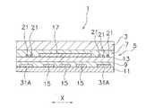
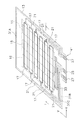
図1に示すタッチパネル1は、カバー部材3と、カバー部材3の裏面側に貼り付けられたフィルムセンサ5と、を備えている。
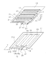
第1基材フィルム11と第2基材フィルム13は、上下方向に並んで配置されている。この実施形態では、第1基材フィルム11が下方であり、第2基材フィルム13が上方である。
複数の第1透明電極15は、第1基材フィルム11上に並設される。複数の第1透明電極15は、第1基材フィルム11に形成され、Y方向に延び、X方向に所定の間隔をあけて配列された電極である。
なお、第1透明電極15及び第2透明電極17は、は直線形状に限定されるものではなく、例えば、波形状であっても、太さが途中で変わるようなものであってもよい。
なお、この実施形態では、第1透明電極15は3つ、第2透明電極17は6つ設けられているが、その数は特に制限されず複数あればよい。
なお、接続端子25及び接続端子27は、第1基材フィルム11及び第2基材フィルム13の延出部41にそれぞれ配置されている。接続端子25及び接続端子27には、フレキシブルプリント配線基板(図示せず)が接続されており、図示しない検出制御部の検出回路に電気的に接続されている。
第1シールド層31A及び第2シールド層31Bはそれぞれ、一端がグランド線に接続されている。
第1シールド層31A及び第2シールド層31Bは、第1透明電極15と同様の材料からなる透明導電膜を全面的に又はメッシュ状に形成したものを用いることができる。
第2シールド層31Bは、第1シールド層31Aの先端近傍(つまり、第1基材フィルム11の第4隅の近傍)からX方向に延びている。したがって、第2シールド層31Bは、最も図左側の第1引出し配線19の第1部分19a及び第2部分19bに近接している。第2シールド層31Bと第1シールド層31Aとの間には隙間31Cが確保されており、つまり両者は絶縁されている。
第1シールド層31Aと第2シールド層31Bを作成する際に、例えばスクリーン印刷によって全体を一度に形成した後に、両者を分断することで第1シールド層31A及び第2シールド層31Bとを得ることができる。
第1シールド層31A及び第2シールド層31Bは、特定範囲内の複数の周波数に対して共振現象を生じさせないために、各周波数のλ/n(n=2,4,6,・・・)となる長さを含まないように長さ範囲が設定されている。
c:電波の速度3x10^8m
λ:波長=n×長さ
n=2,4,6,,,
対象となる周波数帯の一例としては、TEMセル法における100MHz〜400MHzがある。TEMセル試験は、車載電子機器試験の一つであり、ラジオ/TV放送、トランシーバ、及びアマチュア無線などの無線電波に対するイミュニティ試験である。TEMセル試験では、想定される電波をTEMセル内にて放射し、車載商品が影響を受けないかを確認する。
100MHz〜400MHzを上記式に代入して、1/4ラムダ(n=4)の場合、
3x10^8/100x10^6/4=750mm
3x10^8/400x10^6/4=187.5mm
となり、シールド層が187.5mm〜750mmの長さ範囲を避けることが好ましいことが分かる。
このタッチパネル1では、第1シールド層31A及び第2シールド層31Bの長さが上記の条件を満たしているので、第1シールド層31A及び第2シールド層31Bが電磁波に対して共振しにくい。したがって、複数の第1引出し配線19にノイズが発生しにくい。
なお、上述の周波数及びシールド層の長さは例示であり、本発明はそのような実施形態に限定されない。
第3シールド層33はグランド線に接続されている。
第3シールド層33は、第2透明電極17同様の材料からなる透明導電膜を全面的に又はメッシュ状に形成したものを用いることができる。
以上、本発明の一実施形態について説明したが、本発明は上記実施形態に限定されるものではなく、発明の要旨を逸脱しない範囲で種々の変更が可能である。特に、本明細書に書かれた複数の実施形態及び変形例は必要に応じて任意に組み合せ可能である。
前記実施形態では第1シールド層31Aと第2シールド層31Bは第1基材フィルム11の第4隅付近で切断されていたが、切断箇所及び切断形状は特に限定されない。
前記第1シールド層31Aと第2シールド層31Bは、第1基材フィルムに形成されていたが、第2基材フィルムに形成されてもよい。
前記実施形態では接続端子25はX方向片側にずれて配置されていたが、接続端子25はX方向中央部分に配置されていてもよい。
前記実施形態では、2種類の透明電極はそれぞれ2枚の基材フィルムに設けられていたが、本発明はそのような実施形態に限定されない。例えば、2種類の透明電極は1枚の基材フィルムの片面又は両面に設けられていてもよい。
5 :フィルムセンサ
11 :第1基材フィルム
13 :第2基材フィルム
15 :第1透明電極
17 :第2透明電極
19 :第1引出し配線
21 :第2引出し配線
31A :第1シールド層
31B :第2シールド層
Claims (3)
- 基材と、
前記基材上に形成され、一方向に延びる複数の第1検出電極と、
前記基材上に形成され、前記複数の第1検出電極に接続された複数の第1配線と、
前記複数の第1検出電極に交差するように形成された複数の第2検出電極と、
前記複数の第2検出電極に接続され、フレキシブルプリント配線基板との接続端子に至るまで延びている複数の第2配線と、
前記基材上に形成され、平面視で前記複数の第2配線に重なるように延びている形状で配置され、特定範囲内の複数の周波数に対して共振現象を生じさせないために、各周波数のλ/n(n=2,4,6,・・・)となる長さを含まないように延びの長さ範囲が設定されている、シールド層と、
を備えたタッチパネル。
- 前記シールド層は、第1シールド層と、前記第1シールド層から絶縁された第2シールド層を有しており、
前記第1シールド層及び前記第2シールド層は、各周波数のλ/n(n=2,4,6,・・・)となる長さを含まないように長さ範囲が設定されている、請求項1に記載のタッチパネル。 - 前記シールド層は、前記複数の第1検出電極及び前記複数の第1配線を囲うように前記基材の周縁部に配置されている、請求項1又は請求項2に記載のタッチパネル。
Priority Applications (6)
| Application Number | Priority Date | Filing Date | Title |
|---|---|---|---|
| JP2014265914A JP5989757B2 (ja) | 2014-12-26 | 2014-12-26 | タッチパネル |
| CN201580068509.2A CN107003780B (zh) | 2014-12-26 | 2015-11-26 | 触控面板 |
| KR1020177015682A KR102093940B1 (ko) | 2014-12-26 | 2015-11-26 | 터치 패널 |
| PCT/JP2015/083182 WO2016104035A1 (ja) | 2014-12-26 | 2015-11-26 | タッチパネル |
| EP15872604.2A EP3232302B1 (en) | 2014-12-26 | 2015-11-26 | Touch panel |
| US15/537,539 US9996206B2 (en) | 2014-12-26 | 2015-11-26 | Touch panel |
Applications Claiming Priority (1)
| Application Number | Priority Date | Filing Date | Title |
|---|---|---|---|
| JP2014265914A JP5989757B2 (ja) | 2014-12-26 | 2014-12-26 | タッチパネル |
Publications (2)
| Publication Number | Publication Date |
|---|---|
| JP2016126470A JP2016126470A (ja) | 2016-07-11 |
| JP5989757B2 true JP5989757B2 (ja) | 2016-09-07 |
Family
ID=56150067
Family Applications (1)
| Application Number | Title | Priority Date | Filing Date |
|---|---|---|---|
| JP2014265914A Active JP5989757B2 (ja) | 2014-12-26 | 2014-12-26 | タッチパネル |
Country Status (6)
| Country | Link |
|---|---|
| US (1) | US9996206B2 (ja) |
| EP (1) | EP3232302B1 (ja) |
| JP (1) | JP5989757B2 (ja) |
| KR (1) | KR102093940B1 (ja) |
| CN (1) | CN107003780B (ja) |
| WO (1) | WO2016104035A1 (ja) |
Families Citing this family (2)
| Publication number | Priority date | Publication date | Assignee | Title |
|---|---|---|---|---|
| KR102843273B1 (ko) | 2019-12-20 | 2025-08-06 | 삼성디스플레이 주식회사 | 표시 장치 |
| CN112987974B (zh) * | 2021-03-29 | 2025-04-29 | 南京华睿川电子科技有限公司 | 一种抗干扰电容式触摸屏功能片 |
Family Cites Families (14)
| Publication number | Priority date | Publication date | Assignee | Title |
|---|---|---|---|---|
| JPS58182744A (ja) * | 1982-04-20 | 1983-10-25 | Fujitsu Ltd | 座標検出装置 |
| JP2007335781A (ja) * | 2006-06-19 | 2007-12-27 | Mitsubishi Cable Ind Ltd | 電磁波遮蔽材 |
| GB2460288B (en) * | 2006-06-19 | 2012-02-22 | Mitsubishi Cable Ind Ltd | Electromagnetic shielding material and electromagnetic absorber |
| TW201145132A (en) * | 2010-03-11 | 2011-12-16 | Alps Electric Co Ltd | Translucent inputting device |
| JP5540797B2 (ja) * | 2010-03-19 | 2014-07-02 | ソニー株式会社 | センサ装置および表示装置 |
| US8723053B2 (en) * | 2011-03-09 | 2014-05-13 | Select Fabricators, Inc. | Electromagnetically shielded enclosure with operable interfaces |
| JP5168377B2 (ja) | 2011-03-24 | 2013-03-21 | 大日本印刷株式会社 | タッチパネルセンサおよびタッチパネルセンサの製造方法 |
| US8508956B2 (en) * | 2011-05-05 | 2013-08-13 | Carefusion 303, Inc. | Modular shielded electronics enclosure |
| US9033739B2 (en) * | 2011-09-09 | 2015-05-19 | Apple Inc. | Techniques for shielding connectors that allow for conformal coating against corrosion |
| CN104396358A (zh) | 2012-04-18 | 2015-03-04 | 柯尼卡美能达株式会社 | 透光性导电图案部件及使用了其的透光性电磁屏蔽·天线部件 |
| US20140028619A1 (en) * | 2012-07-30 | 2014-01-30 | Lenovo (Beijing) Co., Ltd. | Touch Sensitive Apparatus, Mobile Terminal And Terminal Device |
| KR20150073350A (ko) * | 2013-12-23 | 2015-07-01 | 에스케이하이닉스 주식회사 | 전자기간섭 차폐층을 갖는 반도체 패키지 및 그 제조방법 |
| GB2521835A (en) * | 2014-01-02 | 2015-07-08 | Nokia Technologies Oy | Electromagnetic shielding |
| JP6688133B2 (ja) * | 2016-03-31 | 2020-04-28 | 三菱重工機械システム株式会社 | 料金収受機、料金収受方法及びプログラム |
-
2014
- 2014-12-26 JP JP2014265914A patent/JP5989757B2/ja active Active
-
2015
- 2015-11-26 EP EP15872604.2A patent/EP3232302B1/en active Active
- 2015-11-26 WO PCT/JP2015/083182 patent/WO2016104035A1/ja not_active Ceased
- 2015-11-26 KR KR1020177015682A patent/KR102093940B1/ko active Active
- 2015-11-26 US US15/537,539 patent/US9996206B2/en active Active
- 2015-11-26 CN CN201580068509.2A patent/CN107003780B/zh active Active
Also Published As
| Publication number | Publication date |
|---|---|
| KR20170098817A (ko) | 2017-08-30 |
| EP3232302A1 (en) | 2017-10-18 |
| EP3232302B1 (en) | 2020-01-01 |
| EP3232302A4 (en) | 2018-01-24 |
| WO2016104035A1 (ja) | 2016-06-30 |
| CN107003780B (zh) | 2019-01-08 |
| JP2016126470A (ja) | 2016-07-11 |
| US9996206B2 (en) | 2018-06-12 |
| KR102093940B1 (ko) | 2020-03-26 |
| CN107003780A (zh) | 2017-08-01 |
| US20170351356A1 (en) | 2017-12-07 |
Similar Documents
| Publication | Publication Date | Title |
|---|---|---|
| JP6262703B2 (ja) | スマートフォン | |
| US8717332B2 (en) | Planar element, and touch switch | |
| CN105765501B (zh) | 导电片、静电电容式触摸面板和显示装置 | |
| KR101093651B1 (ko) | 금속박막을 이용한 터치패널 및 그 제조방법 | |
| EP3258356A1 (en) | Touch input device and electrode sheet | |
| JP2013041573A (ja) | 静電容量方式タッチパネルおよび静電容量方式タッチパネルにおける金属ジャンパの視認性の減少方法 | |
| KR101357586B1 (ko) | 터치 패널 | |
| CN105718114A (zh) | 智能手机 | |
| JP6084117B2 (ja) | タッチパネル、表示装置及び電子機器 | |
| KR20190044625A (ko) | 터치 패널용 부재 | |
| KR101103536B1 (ko) | 강화유리 일면에 두 층의 투명도전막을 갖는 정전용량방식 터치패널 및 그 제조방법 | |
| JP5989757B2 (ja) | タッチパネル | |
| KR20130116854A (ko) | 터치윈도우 | |
| JP2014170342A (ja) | 静電容量式入力装置 | |
| JP6134965B2 (ja) | タッチパネル装置 | |
| US9342171B2 (en) | Touch panel with first and second electrodes extending in the same direction but on opposite surfaces of a substrate | |
| JP6134968B2 (ja) | 表示装置 | |
| JP6180174B2 (ja) | タッチパネル、表示装置及び電子機器 | |
| CN202649985U (zh) | 透明电容触摸板的电磁屏蔽结构 | |
| KR101916306B1 (ko) | 터치 패널 | |
| JP2015210554A (ja) | タッチスクリーン、タッチパネル、表示装置、および電子機器 | |
| JP2013148941A (ja) | 静電容量式タッチパネル及びその生産方法 | |
| JP2012226498A (ja) | タッチスイッチ | |
| JP2015149094A (ja) | 静電容量式入力装置 | |
| JP2014174656A (ja) | タッチパネル用電極部材、タッチパネル、及び画像表示装置 |
Legal Events
| Date | Code | Title | Description |
|---|---|---|---|
| A621 | Written request for application examination |
Free format text: JAPANESE INTERMEDIATE CODE: A621 Effective date: 20160408 |
|
| A871 | Explanation of circumstances concerning accelerated examination |
Free format text: JAPANESE INTERMEDIATE CODE: A871 Effective date: 20160408 |
|
| A975 | Report on accelerated examination |
Free format text: JAPANESE INTERMEDIATE CODE: A971005 Effective date: 20160506 |
|
| A131 | Notification of reasons for refusal |
Free format text: JAPANESE INTERMEDIATE CODE: A131 Effective date: 20160531 |
|
| A521 | Request for written amendment filed |
Free format text: JAPANESE INTERMEDIATE CODE: A523 Effective date: 20160705 |
|
| TRDD | Decision of grant or rejection written | ||
| A01 | Written decision to grant a patent or to grant a registration (utility model) |
Free format text: JAPANESE INTERMEDIATE CODE: A01 Effective date: 20160809 |
|
| A61 | First payment of annual fees (during grant procedure) |
Free format text: JAPANESE INTERMEDIATE CODE: A61 Effective date: 20160810 |
|
| R150 | Certificate of patent or registration of utility model |
Ref document number: 5989757 Country of ref document: JP Free format text: JAPANESE INTERMEDIATE CODE: R150 |
|
| S533 | Written request for registration of change of name |
Free format text: JAPANESE INTERMEDIATE CODE: R313533 |
|
| R350 | Written notification of registration of transfer |
Free format text: JAPANESE INTERMEDIATE CODE: R350 |
|
| R250 | Receipt of annual fees |
Free format text: JAPANESE INTERMEDIATE CODE: R250 |
|
| R250 | Receipt of annual fees |
Free format text: JAPANESE INTERMEDIATE CODE: R250 |
|
| R250 | Receipt of annual fees |
Free format text: JAPANESE INTERMEDIATE CODE: R250 |
|
| R250 | Receipt of annual fees |
Free format text: JAPANESE INTERMEDIATE CODE: R250 |
|
| R250 | Receipt of annual fees |
Free format text: JAPANESE INTERMEDIATE CODE: R250 |
|
| R250 | Receipt of annual fees |
Free format text: JAPANESE INTERMEDIATE CODE: R250 |
|
| R250 | Receipt of annual fees |
Free format text: JAPANESE INTERMEDIATE CODE: R250 |