JP5975418B2 - イオン注入方法 - Google Patents
イオン注入方法 Download PDFInfo
- Publication number
- JP5975418B2 JP5975418B2 JP2012003960A JP2012003960A JP5975418B2 JP 5975418 B2 JP5975418 B2 JP 5975418B2 JP 2012003960 A JP2012003960 A JP 2012003960A JP 2012003960 A JP2012003960 A JP 2012003960A JP 5975418 B2 JP5975418 B2 JP 5975418B2
- Authority
- JP
- Japan
- Prior art keywords
- ions
- ion
- integer
- wafer
- gas supply
- Prior art date
- Legal status (The legal status is an assumption and is not a legal conclusion. Google has not performed a legal analysis and makes no representation as to the accuracy of the status listed.)
- Active
Links
- 238000000034 method Methods 0.000 title claims description 18
- 238000005468 ion implantation Methods 0.000 title claims description 14
- 150000002500 ions Chemical class 0.000 claims description 99
- 239000002994 raw material Substances 0.000 claims description 18
- LPIQUOYDBNQMRZ-UHFFFAOYSA-N cyclopentene Chemical compound C1CC=CC1 LPIQUOYDBNQMRZ-UHFFFAOYSA-N 0.000 claims description 14
- KAKZBPTYRLMSJV-UHFFFAOYSA-N Butadiene Chemical compound C=CC=C KAKZBPTYRLMSJV-UHFFFAOYSA-N 0.000 claims description 12
- 238000001819 mass spectrum Methods 0.000 claims description 11
- XDTMQSROBMDMFD-UHFFFAOYSA-N Cyclohexane Chemical compound C1CCCCC1 XDTMQSROBMDMFD-UHFFFAOYSA-N 0.000 claims description 9
- RGSFGYAAUTVSQA-UHFFFAOYSA-N pentamethylene Natural products C1CCCC1 RGSFGYAAUTVSQA-UHFFFAOYSA-N 0.000 claims description 9
- 238000004458 analytical method Methods 0.000 claims description 8
- 229910052710 silicon Inorganic materials 0.000 claims description 2
- 239000010703 silicon Substances 0.000 claims description 2
- 238000010884 ion-beam technique Methods 0.000 description 22
- 238000000605 extraction Methods 0.000 description 8
- QWUWMCYKGHVNAV-UHFFFAOYSA-N 1,2-dihydrostilbene Chemical group C=1C=CC=CC=1CCC1=CC=CC=C1 QWUWMCYKGHVNAV-UHFFFAOYSA-N 0.000 description 7
- -1 carbon molecular ions Chemical class 0.000 description 7
- 229910052799 carbon Inorganic materials 0.000 description 6
- 238000010438 heat treatment Methods 0.000 description 4
- 238000009835 boiling Methods 0.000 description 3
- 230000008569 process Effects 0.000 description 3
- 230000008901 benefit Effects 0.000 description 2
- 239000007788 liquid Substances 0.000 description 2
- 238000004519 manufacturing process Methods 0.000 description 2
- 230000007246 mechanism Effects 0.000 description 2
- 239000004065 semiconductor Substances 0.000 description 2
- XUIMIQQOPSSXEZ-UHFFFAOYSA-N Silicon Chemical compound [Si] XUIMIQQOPSSXEZ-UHFFFAOYSA-N 0.000 description 1
- 238000000137 annealing Methods 0.000 description 1
- 150000001793 charged compounds Chemical class 0.000 description 1
- 239000013078 crystal Substances 0.000 description 1
- 230000007547 defect Effects 0.000 description 1
- 230000005684 electric field Effects 0.000 description 1
- 238000005516 engineering process Methods 0.000 description 1
- 239000000284 extract Substances 0.000 description 1
- DMEGYFMYUHOHGS-UHFFFAOYSA-N heptamethylene Natural products C1CCCCCC1 DMEGYFMYUHOHGS-UHFFFAOYSA-N 0.000 description 1
- 238000004949 mass spectrometry Methods 0.000 description 1
- 239000000463 material Substances 0.000 description 1
- 238000012986 modification Methods 0.000 description 1
- 230000004048 modification Effects 0.000 description 1
- 239000011343 solid material Substances 0.000 description 1
- 230000001629 suppression Effects 0.000 description 1
Images


Classifications
-
- H—ELECTRICITY
- H01—ELECTRIC ELEMENTS
- H01L—SEMICONDUCTOR DEVICES NOT COVERED BY CLASS H10
- H01L21/00—Processes or apparatus adapted for the manufacture or treatment of semiconductor or solid state devices or of parts thereof
- H01L21/02—Manufacture or treatment of semiconductor devices or of parts thereof
- H01L21/04—Manufacture or treatment of semiconductor devices or of parts thereof the devices having at least one potential-jump barrier or surface barrier, e.g. PN junction, depletion layer or carrier concentration layer
- H01L21/18—Manufacture or treatment of semiconductor devices or of parts thereof the devices having at least one potential-jump barrier or surface barrier, e.g. PN junction, depletion layer or carrier concentration layer the devices having semiconductor bodies comprising elements of Group IV of the Periodic System or AIIIBV compounds with or without impurities, e.g. doping materials
- H01L21/26—Bombardment with radiation
- H01L21/263—Bombardment with radiation with high-energy radiation
- H01L21/265—Bombardment with radiation with high-energy radiation producing ion implantation
- H01L21/2658—Bombardment with radiation with high-energy radiation producing ion implantation of a molecular ion, e.g. decaborane
-
- H—ELECTRICITY
- H01—ELECTRIC ELEMENTS
- H01L—SEMICONDUCTOR DEVICES NOT COVERED BY CLASS H10
- H01L21/00—Processes or apparatus adapted for the manufacture or treatment of semiconductor or solid state devices or of parts thereof
- H01L21/02—Manufacture or treatment of semiconductor devices or of parts thereof
- H01L21/04—Manufacture or treatment of semiconductor devices or of parts thereof the devices having at least one potential-jump barrier or surface barrier, e.g. PN junction, depletion layer or carrier concentration layer
- H01L21/18—Manufacture or treatment of semiconductor devices or of parts thereof the devices having at least one potential-jump barrier or surface barrier, e.g. PN junction, depletion layer or carrier concentration layer the devices having semiconductor bodies comprising elements of Group IV of the Periodic System or AIIIBV compounds with or without impurities, e.g. doping materials
- H01L21/26—Bombardment with radiation
- H01L21/263—Bombardment with radiation with high-energy radiation
- H01L21/265—Bombardment with radiation with high-energy radiation producing ion implantation
-
- H—ELECTRICITY
- H01—ELECTRIC ELEMENTS
- H01J—ELECTRIC DISCHARGE TUBES OR DISCHARGE LAMPS
- H01J37/00—Discharge tubes with provision for introducing objects or material to be exposed to the discharge, e.g. for the purpose of examination or processing thereof
- H01J37/02—Details
- H01J37/04—Arrangements of electrodes and associated parts for generating or controlling the discharge, e.g. electron-optical arrangement, ion-optical arrangement
- H01J37/08—Ion sources; Ion guns
-
- H—ELECTRICITY
- H01—ELECTRIC ELEMENTS
- H01J—ELECTRIC DISCHARGE TUBES OR DISCHARGE LAMPS
- H01J37/00—Discharge tubes with provision for introducing objects or material to be exposed to the discharge, e.g. for the purpose of examination or processing thereof
- H01J37/30—Electron-beam or ion-beam tubes for localised treatment of objects
- H01J37/317—Electron-beam or ion-beam tubes for localised treatment of objects for changing properties of the objects or for applying thin layers thereon, e.g. for ion implantation
- H01J37/3171—Electron-beam or ion-beam tubes for localised treatment of objects for changing properties of the objects or for applying thin layers thereon, e.g. for ion implantation for ion implantation
-
- H—ELECTRICITY
- H01—ELECTRIC ELEMENTS
- H01L—SEMICONDUCTOR DEVICES NOT COVERED BY CLASS H10
- H01L21/00—Processes or apparatus adapted for the manufacture or treatment of semiconductor or solid state devices or of parts thereof
- H01L21/02—Manufacture or treatment of semiconductor devices or of parts thereof
- H01L21/04—Manufacture or treatment of semiconductor devices or of parts thereof the devices having at least one potential-jump barrier or surface barrier, e.g. PN junction, depletion layer or carrier concentration layer
- H01L21/18—Manufacture or treatment of semiconductor devices or of parts thereof the devices having at least one potential-jump barrier or surface barrier, e.g. PN junction, depletion layer or carrier concentration layer the devices having semiconductor bodies comprising elements of Group IV of the Periodic System or AIIIBV compounds with or without impurities, e.g. doping materials
- H01L21/26—Bombardment with radiation
- H01L21/263—Bombardment with radiation with high-energy radiation
- H01L21/265—Bombardment with radiation with high-energy radiation producing ion implantation
- H01L21/26506—Bombardment with radiation with high-energy radiation producing ion implantation in group IV semiconductors
-
- H—ELECTRICITY
- H01—ELECTRIC ELEMENTS
- H01J—ELECTRIC DISCHARGE TUBES OR DISCHARGE LAMPS
- H01J2237/00—Discharge tubes exposing object to beam, e.g. for analysis treatment, etching, imaging
- H01J2237/006—Details of gas supplies, e.g. in an ion source, to a beam line, to a specimen or to a workpiece
Description
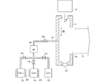
図2の説明では、イオン源チャンバー4の外側に永久磁石を配置する構成について説明したが、イオン源チャンバー4の容積が小さい場合、このような永久磁石がなくとも電子eはイオン源チャンバー4内に行き届く為、この永久磁石は特段設けておく必要はない。
2・・・ウエハ
3・・・イオンビーム
4・・・イオン源チャンバー
5・・・引出し電極系
12・・・電子銃
13・・・第一のガス供給源
14・・・第二のガス供給源
15・・・第三のガス供給源
Claims (1)
- C 6 H 12 (シクロヘキサン)、C 5 H 8 (シクロペンテン)又はC 4 H 6 (ブタジエン)のいずれか1つのイオン生成用原料をイオン化し、質量分析の後、質量スペクトルにおける相対存在量比のピークが20%以上であるC4H x (xは1以上の整数)、C5H x (xは1以上の整数)またはC6H x (xは1以上の整数)のいずれかの正イオンをウエハに注入するイオン注入方法。
Priority Applications (4)
| Application Number | Priority Date | Filing Date | Title |
|---|---|---|---|
| JP2012003960A JP5975418B2 (ja) | 2011-03-25 | 2012-01-12 | イオン注入方法 |
| KR1020120029260A KR101371957B1 (ko) | 2011-03-25 | 2012-03-22 | 이온 주입 방법 |
| TW101110085A TWI457988B (zh) | 2011-03-25 | 2012-03-23 | 離子植入方法 |
| US13/428,481 US8921240B2 (en) | 2011-03-25 | 2012-03-23 | Ion implantation method |
Applications Claiming Priority (3)
| Application Number | Priority Date | Filing Date | Title |
|---|---|---|---|
| JP2011068307 | 2011-03-25 | ||
| JP2011068307 | 2011-03-25 | ||
| JP2012003960A JP5975418B2 (ja) | 2011-03-25 | 2012-01-12 | イオン注入方法 |
Publications (3)
| Publication Number | Publication Date |
|---|---|
| JP2012216767A JP2012216767A (ja) | 2012-11-08 |
| JP2012216767A5 JP2012216767A5 (ja) | 2015-02-19 |
| JP5975418B2 true JP5975418B2 (ja) | 2016-08-23 |
Family
ID=46877709
Family Applications (1)
| Application Number | Title | Priority Date | Filing Date |
|---|---|---|---|
| JP2012003960A Active JP5975418B2 (ja) | 2011-03-25 | 2012-01-12 | イオン注入方法 |
Country Status (4)
| Country | Link |
|---|---|
| US (1) | US8921240B2 (ja) |
| JP (1) | JP5975418B2 (ja) |
| KR (1) | KR101371957B1 (ja) |
| TW (1) | TWI457988B (ja) |
Families Citing this family (2)
| Publication number | Priority date | Publication date | Assignee | Title |
|---|---|---|---|---|
| CN107078028A (zh) | 2014-06-24 | 2017-08-18 | Ev 集团 E·索尔纳有限责任公司 | 用于衬底的表面处理的方法和设备 |
| JP2019091923A (ja) * | 2019-02-07 | 2019-06-13 | エーファウ・グループ・エー・タルナー・ゲーエムベーハー | 基板を表面処理するための方法及び装置 |
Family Cites Families (10)
| Publication number | Priority date | Publication date | Assignee | Title |
|---|---|---|---|---|
| JP4096373B2 (ja) * | 1997-03-25 | 2008-06-04 | 住友電気工業株式会社 | 硬質被膜とその製造方法 |
| US7465478B2 (en) | 2000-08-11 | 2008-12-16 | Applied Materials, Inc. | Plasma immersion ion implantation process |
| US6686595B2 (en) | 2002-06-26 | 2004-02-03 | Semequip Inc. | Electron impact ion source |
| US7312162B2 (en) * | 2005-05-17 | 2007-12-25 | Applied Materials, Inc. | Low temperature plasma deposition process for carbon layer deposition |
| KR101455404B1 (ko) * | 2005-12-09 | 2014-10-27 | 세미이큅, 인코포레이티드 | 탄소 클러스터의 주입에 의한 반도체 디바이스의 제조를위한 시스템 및 방법 |
| US8183161B2 (en) * | 2006-09-12 | 2012-05-22 | Tokyo Electron Limited | Method and system for dry etching a hafnium containing material |
| JP2010062529A (ja) * | 2008-08-04 | 2010-03-18 | Toshiba Corp | 半導体装置の製造方法 |
| TWI522404B (zh) * | 2009-03-26 | 2016-02-21 | Lintec Corp | A molded body, a manufacturing method thereof, an electronic device element, and an electronic device |
| US8992785B2 (en) * | 2010-01-15 | 2015-03-31 | Tel Epion Inc. | Method for modifying an etch rate of a material layer using energetic charged particles |
| US8343860B1 (en) * | 2010-03-23 | 2013-01-01 | L'air Liquide Societe Anonyme Pour L'etude Et L'exploitation Des Procedes Georges Claude | High C content molecules for C implant |
-
2012
- 2012-01-12 JP JP2012003960A patent/JP5975418B2/ja active Active
- 2012-03-22 KR KR1020120029260A patent/KR101371957B1/ko active IP Right Grant
- 2012-03-23 TW TW101110085A patent/TWI457988B/zh not_active IP Right Cessation
- 2012-03-23 US US13/428,481 patent/US8921240B2/en not_active Expired - Fee Related
Also Published As
| Publication number | Publication date |
|---|---|
| TWI457988B (zh) | 2014-10-21 |
| JP2012216767A (ja) | 2012-11-08 |
| US20120244724A1 (en) | 2012-09-27 |
| US8921240B2 (en) | 2014-12-30 |
| TW201239957A (en) | 2012-10-01 |
| KR101371957B1 (ko) | 2014-03-07 |
| KR20120109356A (ko) | 2012-10-08 |
Similar Documents
| Publication | Publication Date | Title |
|---|---|---|
| JP4875883B2 (ja) | イオン化したクラスタ、分子及び単一原子を発生するためのイオン発生装置 | |
| TWI404128B (zh) | 離子植入裝置及由碳硼烷聚集物離子衍生之離子植入的半導體製造方法 | |
| TW511113B (en) | Ion implantation with high brightness, low emittance ion source, acceleration-deceleration transport system and improved ion source construction | |
| KR100864048B1 (ko) | 이온 소스 | |
| KR101593540B1 (ko) | 폭이 넓은 리본 이온 빔 발생을 위한 고밀도 헬리콘 플라즈마 소스 | |
| TW201142908A (en) | Techniques for generating uniform ion beam | |
| US20070178678A1 (en) | Methods of implanting ions and ion sources used for same | |
| US20070178679A1 (en) | Methods of implanting ions and ion sources used for same | |
| TW201407655A (zh) | 離子源及清洗離子源的方法 | |
| TW201234406A (en) | Implementation of co-gases for germanium and boron ion implants | |
| JP2004063415A (ja) | イオン注入方法及びsoiウエハの製造方法、並びにイオン注入装置 | |
| CN1477984A (zh) | 离子注入系统及控制方法 | |
| TWI446394B (zh) | 離子源及離子植入系統 | |
| TW497159B (en) | System and method for removing contaminant particles relative to an ion beam | |
| JP5975418B2 (ja) | イオン注入方法 | |
| JP5524070B2 (ja) | ダブルプラズマイオンソース | |
| KR20220011661A (ko) | 이온 주입 시스템용 개선된 전하 스트리핑 | |
| WO2013068796A2 (en) | Molecular ion source for ion implantation | |
| CN103165391A (zh) | 一种高价离子源的调制装置 | |
| WO2014159402A1 (en) | Ion source | |
| JP2013187017A (ja) | 半導体装置の製造装置および製造方法 | |
| JP7464781B2 (ja) | イオン生成装置およびイオン注入装置 | |
| JP2014086137A (ja) | コールドカソード型イオン源 | |
| TWI263249B (en) | An ion implantation device and a method of semiconductor manufacturing by the implantation of boron hydride cluster ions | |
| CN113178371A (zh) | 一种用于生产离子簇、电离分子和电离单原子的离子源 |
Legal Events
| Date | Code | Title | Description |
|---|---|---|---|
| A521 | Request for written amendment filed |
Free format text: JAPANESE INTERMEDIATE CODE: A523 Effective date: 20130808 |
|
| A521 | Request for written amendment filed |
Free format text: JAPANESE INTERMEDIATE CODE: A523 Effective date: 20141215 |
|
| A621 | Written request for application examination |
Free format text: JAPANESE INTERMEDIATE CODE: A621 Effective date: 20141224 |
|
| A521 | Request for written amendment filed |
Free format text: JAPANESE INTERMEDIATE CODE: A523 Effective date: 20150401 |
|
| A977 | Report on retrieval |
Free format text: JAPANESE INTERMEDIATE CODE: A971007 Effective date: 20151215 |
|
| A131 | Notification of reasons for refusal |
Free format text: JAPANESE INTERMEDIATE CODE: A131 Effective date: 20160209 |
|
| A521 | Request for written amendment filed |
Free format text: JAPANESE INTERMEDIATE CODE: A523 Effective date: 20160303 |
|
| A521 | Request for written amendment filed |
Free format text: JAPANESE INTERMEDIATE CODE: A523 Effective date: 20160308 |
|
| TRDD | Decision of grant or rejection written | ||
| A01 | Written decision to grant a patent or to grant a registration (utility model) |
Free format text: JAPANESE INTERMEDIATE CODE: A01 Effective date: 20160627 |
|
| R150 | Certificate of patent or registration of utility model |
Ref document number: 5975418 Country of ref document: JP Free format text: JAPANESE INTERMEDIATE CODE: R150 |
|
| A61 | First payment of annual fees (during grant procedure) |
Free format text: JAPANESE INTERMEDIATE CODE: A61 Effective date: 20160710 |
|
| R250 | Receipt of annual fees |
Free format text: JAPANESE INTERMEDIATE CODE: R250 |
|
| R250 | Receipt of annual fees |
Free format text: JAPANESE INTERMEDIATE CODE: R250 |
|
| R250 | Receipt of annual fees |
Free format text: JAPANESE INTERMEDIATE CODE: R250 |
|
| R250 | Receipt of annual fees |
Free format text: JAPANESE INTERMEDIATE CODE: R250 |
|
| R250 | Receipt of annual fees |
Free format text: JAPANESE INTERMEDIATE CODE: R250 |
|
| R250 | Receipt of annual fees |
Free format text: JAPANESE INTERMEDIATE CODE: R250 |