JP5972874B2 - Multi-layer bonding layer for thin wafer handling - Google Patents
Multi-layer bonding layer for thin wafer handling Download PDFInfo
- Publication number
- JP5972874B2 JP5972874B2 JP2013523362A JP2013523362A JP5972874B2 JP 5972874 B2 JP5972874 B2 JP 5972874B2 JP 2013523362 A JP2013523362 A JP 2013523362A JP 2013523362 A JP2013523362 A JP 2013523362A JP 5972874 B2 JP5972874 B2 JP 5972874B2
- Authority
- JP
- Japan
- Prior art keywords
- bonding layer
- layer
- bonding
- substrate
- silicon
- Prior art date
- Legal status (The legal status is an assumption and is not a legal conclusion. Google has not performed a legal analysis and makes no representation as to the accuracy of the status listed.)
- Active
Links
Images


Classifications
-
- B—PERFORMING OPERATIONS; TRANSPORTING
- B32—LAYERED PRODUCTS
- B32B—LAYERED PRODUCTS, i.e. PRODUCTS BUILT-UP OF STRATA OF FLAT OR NON-FLAT, e.g. CELLULAR OR HONEYCOMB, FORM
- B32B38/00—Ancillary operations in connection with laminating processes
- B32B38/0008—Electrical discharge treatment, e.g. corona, plasma treatment; wave energy or particle radiation
-
- B—PERFORMING OPERATIONS; TRANSPORTING
- B32—LAYERED PRODUCTS
- B32B—LAYERED PRODUCTS, i.e. PRODUCTS BUILT-UP OF STRATA OF FLAT OR NON-FLAT, e.g. CELLULAR OR HONEYCOMB, FORM
- B32B38/00—Ancillary operations in connection with laminating processes
- B32B38/10—Removing layers, or parts of layers, mechanically or chemically
-
- B—PERFORMING OPERATIONS; TRANSPORTING
- B32—LAYERED PRODUCTS
- B32B—LAYERED PRODUCTS, i.e. PRODUCTS BUILT-UP OF STRATA OF FLAT OR NON-FLAT, e.g. CELLULAR OR HONEYCOMB, FORM
- B32B43/00—Operations specially adapted for layered products and not otherwise provided for, e.g. repairing; Apparatus therefor
- B32B43/006—Delaminating
-
- H—ELECTRICITY
- H01—ELECTRIC ELEMENTS
- H01L—SEMICONDUCTOR DEVICES NOT COVERED BY CLASS H10
- H01L21/00—Processes or apparatus adapted for the manufacture or treatment of semiconductor or solid state devices or of parts thereof
- H01L21/02—Manufacture or treatment of semiconductor devices or of parts thereof
- H01L21/04—Manufacture or treatment of semiconductor devices or of parts thereof the devices having at least one potential-jump barrier or surface barrier, e.g. PN junction, depletion layer or carrier concentration layer
- H01L21/18—Manufacture or treatment of semiconductor devices or of parts thereof the devices having at least one potential-jump barrier or surface barrier, e.g. PN junction, depletion layer or carrier concentration layer the devices having semiconductor bodies comprising elements of Group IV of the Periodic System or AIIIBV compounds with or without impurities, e.g. doping materials
- H01L21/20—Deposition of semiconductor materials on a substrate, e.g. epitaxial growth solid phase epitaxy
- H01L21/2003—Deposition of semiconductor materials on a substrate, e.g. epitaxial growth solid phase epitaxy characterised by the substrate
- H01L21/2007—Bonding of semiconductor wafers to insulating substrates or to semiconducting substrates using an intermediate insulating layer
-
- H—ELECTRICITY
- H01—ELECTRIC ELEMENTS
- H01L—SEMICONDUCTOR DEVICES NOT COVERED BY CLASS H10
- H01L21/00—Processes or apparatus adapted for the manufacture or treatment of semiconductor or solid state devices or of parts thereof
- H01L21/67—Apparatus specially adapted for handling semiconductor or electric solid state devices during manufacture or treatment thereof; Apparatus specially adapted for handling wafers during manufacture or treatment of semiconductor or electric solid state devices or components ; Apparatus not specifically provided for elsewhere
- H01L21/683—Apparatus specially adapted for handling semiconductor or electric solid state devices during manufacture or treatment thereof; Apparatus specially adapted for handling wafers during manufacture or treatment of semiconductor or electric solid state devices or components ; Apparatus not specifically provided for elsewhere for supporting or gripping
- H01L21/6835—Apparatus specially adapted for handling semiconductor or electric solid state devices during manufacture or treatment thereof; Apparatus specially adapted for handling wafers during manufacture or treatment of semiconductor or electric solid state devices or components ; Apparatus not specifically provided for elsewhere for supporting or gripping using temporarily an auxiliary support
- H01L21/6836—Wafer tapes, e.g. grinding or dicing support tapes
-
- H—ELECTRICITY
- H01—ELECTRIC ELEMENTS
- H01L—SEMICONDUCTOR DEVICES NOT COVERED BY CLASS H10
- H01L24/00—Arrangements for connecting or disconnecting semiconductor or solid-state bodies; Methods or apparatus related thereto
- H01L24/80—Methods for connecting semiconductor or other solid state bodies using means for bonding being attached to, or being formed on, the surface to be connected
- H01L24/83—Methods for connecting semiconductor or other solid state bodies using means for bonding being attached to, or being formed on, the surface to be connected using a layer connector
-
- H—ELECTRICITY
- H01—ELECTRIC ELEMENTS
- H01L—SEMICONDUCTOR DEVICES NOT COVERED BY CLASS H10
- H01L21/00—Processes or apparatus adapted for the manufacture or treatment of semiconductor or solid state devices or of parts thereof
- H01L21/67—Apparatus specially adapted for handling semiconductor or electric solid state devices during manufacture or treatment thereof; Apparatus specially adapted for handling wafers during manufacture or treatment of semiconductor or electric solid state devices or components ; Apparatus not specifically provided for elsewhere
- H01L21/683—Apparatus specially adapted for handling semiconductor or electric solid state devices during manufacture or treatment thereof; Apparatus specially adapted for handling wafers during manufacture or treatment of semiconductor or electric solid state devices or components ; Apparatus not specifically provided for elsewhere for supporting or gripping
- H01L21/6835—Apparatus specially adapted for handling semiconductor or electric solid state devices during manufacture or treatment thereof; Apparatus specially adapted for handling wafers during manufacture or treatment of semiconductor or electric solid state devices or components ; Apparatus not specifically provided for elsewhere for supporting or gripping using temporarily an auxiliary support
-
- H—ELECTRICITY
- H01—ELECTRIC ELEMENTS
- H01L—SEMICONDUCTOR DEVICES NOT COVERED BY CLASS H10
- H01L2221/00—Processes or apparatus adapted for the manufacture or treatment of semiconductor or solid state devices or of parts thereof covered by H01L21/00
- H01L2221/67—Apparatus for handling semiconductor or electric solid state devices during manufacture or treatment thereof; Apparatus for handling wafers during manufacture or treatment of semiconductor or electric solid state devices or components; Apparatus not specifically provided for elsewhere
- H01L2221/683—Apparatus for handling semiconductor or electric solid state devices during manufacture or treatment thereof; Apparatus for handling wafers during manufacture or treatment of semiconductor or electric solid state devices or components; Apparatus not specifically provided for elsewhere for supporting or gripping
- H01L2221/68304—Apparatus for handling semiconductor or electric solid state devices during manufacture or treatment thereof; Apparatus for handling wafers during manufacture or treatment of semiconductor or electric solid state devices or components; Apparatus not specifically provided for elsewhere for supporting or gripping using temporarily an auxiliary support
- H01L2221/68318—Auxiliary support including means facilitating the separation of a device or wafer from the auxiliary support
-
- H—ELECTRICITY
- H01—ELECTRIC ELEMENTS
- H01L—SEMICONDUCTOR DEVICES NOT COVERED BY CLASS H10
- H01L2221/00—Processes or apparatus adapted for the manufacture or treatment of semiconductor or solid state devices or of parts thereof covered by H01L21/00
- H01L2221/67—Apparatus for handling semiconductor or electric solid state devices during manufacture or treatment thereof; Apparatus for handling wafers during manufacture or treatment of semiconductor or electric solid state devices or components; Apparatus not specifically provided for elsewhere
- H01L2221/683—Apparatus for handling semiconductor or electric solid state devices during manufacture or treatment thereof; Apparatus for handling wafers during manufacture or treatment of semiconductor or electric solid state devices or components; Apparatus not specifically provided for elsewhere for supporting or gripping
- H01L2221/68304—Apparatus for handling semiconductor or electric solid state devices during manufacture or treatment thereof; Apparatus for handling wafers during manufacture or treatment of semiconductor or electric solid state devices or components; Apparatus not specifically provided for elsewhere for supporting or gripping using temporarily an auxiliary support
- H01L2221/68327—Apparatus for handling semiconductor or electric solid state devices during manufacture or treatment thereof; Apparatus for handling wafers during manufacture or treatment of semiconductor or electric solid state devices or components; Apparatus not specifically provided for elsewhere for supporting or gripping using temporarily an auxiliary support used during dicing or grinding
-
- H—ELECTRICITY
- H01—ELECTRIC ELEMENTS
- H01L—SEMICONDUCTOR DEVICES NOT COVERED BY CLASS H10
- H01L2221/00—Processes or apparatus adapted for the manufacture or treatment of semiconductor or solid state devices or of parts thereof covered by H01L21/00
- H01L2221/67—Apparatus for handling semiconductor or electric solid state devices during manufacture or treatment thereof; Apparatus for handling wafers during manufacture or treatment of semiconductor or electric solid state devices or components; Apparatus not specifically provided for elsewhere
- H01L2221/683—Apparatus for handling semiconductor or electric solid state devices during manufacture or treatment thereof; Apparatus for handling wafers during manufacture or treatment of semiconductor or electric solid state devices or components; Apparatus not specifically provided for elsewhere for supporting or gripping
- H01L2221/68304—Apparatus for handling semiconductor or electric solid state devices during manufacture or treatment thereof; Apparatus for handling wafers during manufacture or treatment of semiconductor or electric solid state devices or components; Apparatus not specifically provided for elsewhere for supporting or gripping using temporarily an auxiliary support
- H01L2221/6834—Apparatus for handling semiconductor or electric solid state devices during manufacture or treatment thereof; Apparatus for handling wafers during manufacture or treatment of semiconductor or electric solid state devices or components; Apparatus not specifically provided for elsewhere for supporting or gripping using temporarily an auxiliary support used to protect an active side of a device or wafer
-
- H—ELECTRICITY
- H01—ELECTRIC ELEMENTS
- H01L—SEMICONDUCTOR DEVICES NOT COVERED BY CLASS H10
- H01L2221/00—Processes or apparatus adapted for the manufacture or treatment of semiconductor or solid state devices or of parts thereof covered by H01L21/00
- H01L2221/67—Apparatus for handling semiconductor or electric solid state devices during manufacture or treatment thereof; Apparatus for handling wafers during manufacture or treatment of semiconductor or electric solid state devices or components; Apparatus not specifically provided for elsewhere
- H01L2221/683—Apparatus for handling semiconductor or electric solid state devices during manufacture or treatment thereof; Apparatus for handling wafers during manufacture or treatment of semiconductor or electric solid state devices or components; Apparatus not specifically provided for elsewhere for supporting or gripping
- H01L2221/68304—Apparatus for handling semiconductor or electric solid state devices during manufacture or treatment thereof; Apparatus for handling wafers during manufacture or treatment of semiconductor or electric solid state devices or components; Apparatus not specifically provided for elsewhere for supporting or gripping using temporarily an auxiliary support
- H01L2221/68381—Details of chemical or physical process used for separating the auxiliary support from a device or wafer
-
- H—ELECTRICITY
- H01—ELECTRIC ELEMENTS
- H01L—SEMICONDUCTOR DEVICES NOT COVERED BY CLASS H10
- H01L2924/00—Indexing scheme for arrangements or methods for connecting or disconnecting semiconductor or solid-state bodies as covered by H01L24/00
- H01L2924/10—Details of semiconductor or other solid state devices to be connected
- H01L2924/11—Device type
- H01L2924/12—Passive devices, e.g. 2 terminal devices
- H01L2924/1204—Optical Diode
- H01L2924/12041—LED
-
- H—ELECTRICITY
- H01—ELECTRIC ELEMENTS
- H01L—SEMICONDUCTOR DEVICES NOT COVERED BY CLASS H10
- H01L2924/00—Indexing scheme for arrangements or methods for connecting or disconnecting semiconductor or solid-state bodies as covered by H01L24/00
- H01L2924/10—Details of semiconductor or other solid state devices to be connected
- H01L2924/11—Device type
- H01L2924/12—Passive devices, e.g. 2 terminal devices
- H01L2924/1204—Optical Diode
- H01L2924/12042—LASER
-
- H—ELECTRICITY
- H01—ELECTRIC ELEMENTS
- H01L—SEMICONDUCTOR DEVICES NOT COVERED BY CLASS H10
- H01L2924/00—Indexing scheme for arrangements or methods for connecting or disconnecting semiconductor or solid-state bodies as covered by H01L24/00
- H01L2924/10—Details of semiconductor or other solid state devices to be connected
- H01L2924/11—Device type
- H01L2924/14—Integrated circuits
-
- H—ELECTRICITY
- H01—ELECTRIC ELEMENTS
- H01L—SEMICONDUCTOR DEVICES NOT COVERED BY CLASS H10
- H01L2924/00—Indexing scheme for arrangements or methods for connecting or disconnecting semiconductor or solid-state bodies as covered by H01L24/00
- H01L2924/10—Details of semiconductor or other solid state devices to be connected
- H01L2924/146—Mixed devices
- H01L2924/1461—MEMS
-
- H—ELECTRICITY
- H01—ELECTRIC ELEMENTS
- H01L—SEMICONDUCTOR DEVICES NOT COVERED BY CLASS H10
- H01L2924/00—Indexing scheme for arrangements or methods for connecting or disconnecting semiconductor or solid-state bodies as covered by H01L24/00
- H01L2924/30—Technical effects
- H01L2924/35—Mechanical effects
- H01L2924/351—Thermal stress
-
- Y—GENERAL TAGGING OF NEW TECHNOLOGICAL DEVELOPMENTS; GENERAL TAGGING OF CROSS-SECTIONAL TECHNOLOGIES SPANNING OVER SEVERAL SECTIONS OF THE IPC; TECHNICAL SUBJECTS COVERED BY FORMER USPC CROSS-REFERENCE ART COLLECTIONS [XRACs] AND DIGESTS
- Y10—TECHNICAL SUBJECTS COVERED BY FORMER USPC
- Y10T—TECHNICAL SUBJECTS COVERED BY FORMER US CLASSIFICATION
- Y10T156/00—Adhesive bonding and miscellaneous chemical manufacture
- Y10T156/10—Methods of surface bonding and/or assembly therefor
-
- Y—GENERAL TAGGING OF NEW TECHNOLOGICAL DEVELOPMENTS; GENERAL TAGGING OF CROSS-SECTIONAL TECHNOLOGIES SPANNING OVER SEVERAL SECTIONS OF THE IPC; TECHNICAL SUBJECTS COVERED BY FORMER USPC CROSS-REFERENCE ART COLLECTIONS [XRACs] AND DIGESTS
- Y10—TECHNICAL SUBJECTS COVERED BY FORMER USPC
- Y10T—TECHNICAL SUBJECTS COVERED BY FORMER US CLASSIFICATION
- Y10T156/00—Adhesive bonding and miscellaneous chemical manufacture
- Y10T156/11—Methods of delaminating, per se; i.e., separating at bonding face
- Y10T156/1126—Using direct fluid current against work during delaminating
-
- Y—GENERAL TAGGING OF NEW TECHNOLOGICAL DEVELOPMENTS; GENERAL TAGGING OF CROSS-SECTIONAL TECHNOLOGIES SPANNING OVER SEVERAL SECTIONS OF THE IPC; TECHNICAL SUBJECTS COVERED BY FORMER USPC CROSS-REFERENCE ART COLLECTIONS [XRACs] AND DIGESTS
- Y10—TECHNICAL SUBJECTS COVERED BY FORMER USPC
- Y10T—TECHNICAL SUBJECTS COVERED BY FORMER US CLASSIFICATION
- Y10T428/00—Stock material or miscellaneous articles
- Y10T428/24—Structurally defined web or sheet [e.g., overall dimension, etc.]
- Y10T428/24942—Structurally defined web or sheet [e.g., overall dimension, etc.] including components having same physical characteristic in differing degree
-
- Y—GENERAL TAGGING OF NEW TECHNOLOGICAL DEVELOPMENTS; GENERAL TAGGING OF CROSS-SECTIONAL TECHNOLOGIES SPANNING OVER SEVERAL SECTIONS OF THE IPC; TECHNICAL SUBJECTS COVERED BY FORMER USPC CROSS-REFERENCE ART COLLECTIONS [XRACs] AND DIGESTS
- Y10—TECHNICAL SUBJECTS COVERED BY FORMER USPC
- Y10T—TECHNICAL SUBJECTS COVERED BY FORMER US CLASSIFICATION
- Y10T428/00—Stock material or miscellaneous articles
- Y10T428/26—Web or sheet containing structurally defined element or component, the element or component having a specified physical dimension
-
- Y—GENERAL TAGGING OF NEW TECHNOLOGICAL DEVELOPMENTS; GENERAL TAGGING OF CROSS-SECTIONAL TECHNOLOGIES SPANNING OVER SEVERAL SECTIONS OF THE IPC; TECHNICAL SUBJECTS COVERED BY FORMER USPC CROSS-REFERENCE ART COLLECTIONS [XRACs] AND DIGESTS
- Y10—TECHNICAL SUBJECTS COVERED BY FORMER USPC
- Y10T—TECHNICAL SUBJECTS COVERED BY FORMER US CLASSIFICATION
- Y10T428/00—Stock material or miscellaneous articles
- Y10T428/31504—Composite [nonstructural laminate]
- Y10T428/31511—Of epoxy ether
-
- Y—GENERAL TAGGING OF NEW TECHNOLOGICAL DEVELOPMENTS; GENERAL TAGGING OF CROSS-SECTIONAL TECHNOLOGIES SPANNING OVER SEVERAL SECTIONS OF THE IPC; TECHNICAL SUBJECTS COVERED BY FORMER USPC CROSS-REFERENCE ART COLLECTIONS [XRACs] AND DIGESTS
- Y10—TECHNICAL SUBJECTS COVERED BY FORMER USPC
- Y10T—TECHNICAL SUBJECTS COVERED BY FORMER US CLASSIFICATION
- Y10T428/00—Stock material or miscellaneous articles
- Y10T428/31504—Composite [nonstructural laminate]
- Y10T428/31551—Of polyamidoester [polyurethane, polyisocyanate, polycarbamate, etc.]
-
- Y—GENERAL TAGGING OF NEW TECHNOLOGICAL DEVELOPMENTS; GENERAL TAGGING OF CROSS-SECTIONAL TECHNOLOGIES SPANNING OVER SEVERAL SECTIONS OF THE IPC; TECHNICAL SUBJECTS COVERED BY FORMER USPC CROSS-REFERENCE ART COLLECTIONS [XRACs] AND DIGESTS
- Y10—TECHNICAL SUBJECTS COVERED BY FORMER USPC
- Y10T—TECHNICAL SUBJECTS COVERED BY FORMER US CLASSIFICATION
- Y10T428/00—Stock material or miscellaneous articles
- Y10T428/31504—Composite [nonstructural laminate]
- Y10T428/31652—Of asbestos
- Y10T428/31663—As siloxane, silicone or silane
-
- Y—GENERAL TAGGING OF NEW TECHNOLOGICAL DEVELOPMENTS; GENERAL TAGGING OF CROSS-SECTIONAL TECHNOLOGIES SPANNING OVER SEVERAL SECTIONS OF THE IPC; TECHNICAL SUBJECTS COVERED BY FORMER USPC CROSS-REFERENCE ART COLLECTIONS [XRACs] AND DIGESTS
- Y10—TECHNICAL SUBJECTS COVERED BY FORMER USPC
- Y10T—TECHNICAL SUBJECTS COVERED BY FORMER US CLASSIFICATION
- Y10T428/00—Stock material or miscellaneous articles
- Y10T428/31504—Composite [nonstructural laminate]
- Y10T428/31721—Of polyimide
-
- Y—GENERAL TAGGING OF NEW TECHNOLOGICAL DEVELOPMENTS; GENERAL TAGGING OF CROSS-SECTIONAL TECHNOLOGIES SPANNING OVER SEVERAL SECTIONS OF THE IPC; TECHNICAL SUBJECTS COVERED BY FORMER USPC CROSS-REFERENCE ART COLLECTIONS [XRACs] AND DIGESTS
- Y10—TECHNICAL SUBJECTS COVERED BY FORMER USPC
- Y10T—TECHNICAL SUBJECTS COVERED BY FORMER US CLASSIFICATION
- Y10T428/00—Stock material or miscellaneous articles
- Y10T428/31504—Composite [nonstructural laminate]
- Y10T428/31725—Of polyamide
-
- Y—GENERAL TAGGING OF NEW TECHNOLOGICAL DEVELOPMENTS; GENERAL TAGGING OF CROSS-SECTIONAL TECHNOLOGIES SPANNING OVER SEVERAL SECTIONS OF THE IPC; TECHNICAL SUBJECTS COVERED BY FORMER USPC CROSS-REFERENCE ART COLLECTIONS [XRACs] AND DIGESTS
- Y10—TECHNICAL SUBJECTS COVERED BY FORMER USPC
- Y10T—TECHNICAL SUBJECTS COVERED BY FORMER US CLASSIFICATION
- Y10T428/00—Stock material or miscellaneous articles
- Y10T428/31504—Composite [nonstructural laminate]
- Y10T428/31855—Of addition polymer from unsaturated monomers
- Y10T428/31935—Ester, halide or nitrile of addition polymer
-
- Y—GENERAL TAGGING OF NEW TECHNOLOGICAL DEVELOPMENTS; GENERAL TAGGING OF CROSS-SECTIONAL TECHNOLOGIES SPANNING OVER SEVERAL SECTIONS OF THE IPC; TECHNICAL SUBJECTS COVERED BY FORMER USPC CROSS-REFERENCE ART COLLECTIONS [XRACs] AND DIGESTS
- Y10—TECHNICAL SUBJECTS COVERED BY FORMER USPC
- Y10T—TECHNICAL SUBJECTS COVERED BY FORMER US CLASSIFICATION
- Y10T428/00—Stock material or miscellaneous articles
- Y10T428/31504—Composite [nonstructural laminate]
- Y10T428/31855—Of addition polymer from unsaturated monomers
- Y10T428/31938—Polymer of monoethylenically unsaturated hydrocarbon
Description
(米国政府支援研究開発プログラム)
本発明は米陸軍宇宙ミサイル防衛司令部によって与えられた契約番号DASG60−01−C−0047に基づく政府支援の下でなされた。米国政府は本発明において特定の権利を有する。
(US Government supported research and development program)
This invention was made with government support under contract number DASG 60-01-C-0047 awarded by the US Army Space Missile Defense Command. The US government has certain rights in this invention.
(関連出願)
本願は「薄ウェーハーハンドリングのための多層接合層(MULTIPLE BONDING LAYERS FOR THIN−WAFER HANDLING)」と題する、2010年8月6日提出の米国仮出願第61/371,517号の優先権を主張するものであり当該出願全体を引用として本明細書に含める。
(Related application)
This application claims priority to US Provisional Application No. 61 / 371,517, filed Aug. 6, 2010, entitled “MULTIPLE BONDING LAYERS FOR THIN-WAFER HANDING”. And the entire application is incorporated herein by reference.
本発明は、広くは、多層接合システムを利用する新規な暫定ウェーハー接合方法に関する。本発明の方法は、ウェーハーの薄層化及び他の背面処理中にデバイスウェーハーをキャリヤー基板上に支持することができる。 The present invention generally relates to a novel provisional wafer bonding method utilizing a multi-layer bonding system. The method of the present invention can support a device wafer on a carrier substrate during wafer thinning and other backside processing.
集積回路、電力半導体、発光ダイオード、フォトニック回路、マイクロマシン技術(MEMS)、埋込み受動アレイ、パッケージングインタポーザー、ならびに多くの他のシリコンおよび化合物半導体をベースとしたマイクロデバイスは直径1〜12インチの範囲のウェーハー基板の配列内に集合的に製造される。次いでデバイスは個々のデバイスまたはダイスに分けられ、例えば、プリント基板と配線することにより肉眼で見える環境と実用的に接合するように実装される。デバイスパッケージをダイスが未だウェーハー配列の一部である内にその上または周辺に構築することが益々流行りになってきている。この様なやり方は、ウェーハーレベル実装と称され、全体の実装コストを削減するとともに通常なら実際のデバイスの数倍の外形寸法となる従来的な実装に比べデバイスとマイクロエレクトロニック環境の間の配線密度がより高くできる。 Integrated circuits, power semiconductors, light emitting diodes, photonic circuits, micromachine technology (MEMS), embedded passive arrays, packaging interposers, and many other silicon and compound semiconductor based microdevices are 1 to 12 inches in diameter Manufactured collectively in a range of wafer substrate arrays. The devices are then divided into individual devices or dice and mounted so that they are practically bonded to the environment visible to the naked eye, for example by wiring with a printed circuit board. It is becoming increasingly popular to build device packages on or around the dice while the dice are still part of the wafer array. This approach, called wafer level mounting, reduces the overall mounting cost and wiring density between the device and the microelectronic environment compared to conventional mounting, which usually has several times the outer dimensions of the actual device. Can be higher.
最近まで、一般に配線の基本構想は2次元に、つまりデバイスとこれが装着される対応する基板または実装面との間の電気的接続はすべて水平、またはx−y面配置に限定されてきた。いまやマイクロエレクトロニクス産業はデバイスを垂直に、すなわち、z方向にスタックして配線することにより大幅にデバイス配線密度を増加しさらに信号遅延を低減できる(電気接点間の距離を短縮することにより)ことに気付いた。デバイスをスタックするために要求される2つの共通事項は:(1)ウェーハー貫通方向に背面側からデバイスを薄くすること;および(2)続いて、一般にはシリコン貫通ビアまたは「TSV」と称されデバイスの背面で完結するウェーハー貫通の電気接続を形成すること、である。ついでに言うなら、半導体デバイスの薄層化は例えデバイスがスタック配置で実装されない場合でも、放熱を促進するとともに携帯電話のような小型電子製品でずっと小さな形状因子を可能にするため今や標準的技法となってきている。 Until recently, the basic concept of wiring has generally been two-dimensional, i.e., all electrical connections between the device and the corresponding substrate or mounting surface on which it is mounted have been limited to horizontal or xy plane placement. Now, the microelectronics industry can significantly increase device wiring density and reduce signal delay (by shortening the distance between electrical contacts) by wiring the devices vertically, ie, stacked in the z direction. Noticed. Two common requirements for stacking devices are: (1) Thinning the device from the back side in the wafer through direction; and (2) Subsequently, commonly referred to as through silicon vias or “TSV” Forming a through-wafer electrical connection that is completed at the back of the device. Incidentally, thinning of semiconductor devices is now a standard technique to promote heat dissipation and enable much smaller form factors in small electronic products such as mobile phones, even if the devices are not mounted in a stacked configuration. It has become to.
半導体デバイスを100ミクロン未満まで薄くしその断面を削減することに関心が高まっているが、とりわけこれらまたはこれらが属する該当パッケージがスタックされる場合、およびデバイスの背面の電気接続の構成を単純化したい場合にそうである。高容量集積回路の生産に用いられるシリコンウェーハーは一般に直径が200または300mmでウェーハー貫通厚みが約750ミクロンある。薄層化無しでは、表側の回路網と接続する背面側の電気接点をウェーハーを介した接続により形成することはほとんど不可能である。今や、化学エッチングと同様に機械研削(背面研削)および研磨に基づく半導体グレードのシリコンおよび化合物半導体の非常に効率的な薄層化処理工程が商業的に利用されている。これらの処理によりデバイスウェーハーの厚みはウェーハー厚みの横断的な均一性を精密に制御しながら数分で100ミクロン未満まで下げられる。 There is an increasing interest in thinning semiconductor devices to less than 100 microns and reducing their cross-section, but especially when these or the corresponding packages to which they belong are stacked and want to simplify the configuration of electrical connections on the back of the device That is the case. Silicon wafers used in the production of high capacity integrated circuits typically have a diameter of 200 or 300 mm and a wafer penetration thickness of about 750 microns. Without thinning, it is almost impossible to form electrical contacts on the back side connected to the front side network by connection through the wafer. Nowadays, highly efficient thinning processes for semiconductor grade silicon and compound semiconductors based on mechanical grinding (back grinding) and polishing as well as chemical etching are in commercial use. By these processes, the thickness of the device wafer can be reduced to less than 100 microns in a few minutes while precisely controlling the horizontal uniformity of the wafer thickness.
100ミクロン未満まで薄層化されたデバイスウェーハー、とりわけ60ミクロン未満まで薄層化されたものは非常に脆いためその全面積に亘って支持することにより割れや破損を防がなくてはならない。極薄層のデバイスウェーハーを移動するために各種のウェーハーワンドおよびチャックが開発されてきているが、背面研削および、化学的−機械的研磨(CMP)、リソグラフィー、エッチング、蒸着、アニーリング、および洗浄を含むTSV形成処理工程の間にどの様にウェーハーを支持するかという問題がまだ存在し、それはこれらの処理がデバイスウェーハーを薄層化する際またはその後で高い熱的および機械的ストレスをこれに強いるためである。益々流行ってきた極薄ウェーハーの取扱いに対する取組方は十分に厚いデバイスウェーハーを表面を下にして高分子接着剤が付いた剛性キャリヤーに装着することを伴うものである。次いでこの薄層化および処理が背面からなされる。次いで完全に処理された極薄ウェーハーは背面処理が完了してからキャリヤーから熱的、熱力学的または化学的処理により取外されまたは剥離される。 Device wafers thinned to less than 100 microns, especially those thinned to less than 60 microns, are very brittle and must be supported over their entire area to prevent cracking and breakage. Various wafer wands and chucks have been developed for moving ultra-thin device wafers, including back grinding and chemical-mechanical polishing (CMP), lithography, etching, deposition, annealing, and cleaning. There still exists the problem of how to support the wafer during the TSV forming process step, which imposes high thermal and mechanical stress on these processes when or after thinning the device wafer. Because. An increasingly popular approach to handling ultra-thin wafers involves mounting a sufficiently thick device wafer face down on a rigid carrier with a polymeric adhesive. This thinning and processing is then done from the back. The fully processed ultrathin wafer is then removed or stripped from the carrier by thermal, thermodynamic or chemical treatment after the backside processing is complete.
通常のキャリヤー材料にはシリコン(例えば、ブランクのデバイスウェーハー)、ソーダ石灰ガラス、硼珪酸ガラス、サファイヤ、ならびに種々の金属およびセラミックスが含まれる。キャリヤーは方形または矩形でもよいがより一般的にはデバイスウェーハーに合う寸法の円形でこのため接合したアセンブリーは従来の処理工具およびカセットで取り扱える。取外す手段として液体化学薬品を用いて高分子接着剤を溶解または分解する場合には時にはキャリヤーに穿孔して剥離処理工程を速める場合もある。 Typical carrier materials include silicon (eg, blank device wafers), soda lime glass, borosilicate glass, sapphire, and various metals and ceramics. The carrier may be square or rectangular, but more generally is a circle sized to fit the device wafer so that the bonded assembly can be handled with conventional processing tools and cassettes. When dissolving or decomposing a polymer adhesive using liquid chemicals as a means for removal, sometimes the carrier is perforated to speed up the stripping process.
ウェーハーを暫定接合させるために用いられる高分子接着剤は一般に溶液からスピンコートまたはスプレーコートにより塗布されるかまたはドライフィルムのテープとしてラミネートされる。スピンまたはスプレーにより塗布された接着剤の方がテープが提供できるものに比べ厚みの均一性がより高い塗膜を形成するため益々好まれている。厚みの均一性がより高いことは結果的に薄層化の後のウェーハー横断方向の厚みをよりよく制御できることを意味する。高分子はデバイスウェーハーおよびキャリヤーに対し高い接着力を示す。 Polymeric adhesives used to temporarily bond wafers are generally applied from solution by spin coating or spray coating, or laminated as a dry film tape. Adhesives applied by spin or spray are increasingly preferred because they form coatings with greater uniformity of thickness than those that tapes can provide. Higher thickness uniformity means that the thickness across the wafer after thinning can be better controlled as a result. Polymers exhibit high adhesion to device wafers and carriers.
高分子接着剤は必要とされる厚みおよび塗膜の平面性(平坦性)によりデバイスウェーハー上に、キャリヤー上に、または両方にスピンコートすることができる。コーティングされたウェーハーは高分子接着剤層から完全に塗膜溶媒を除去するために焼かれる。次にコーティングされたウェーハーおよびキャリヤーは接合のために接触したまま加熱した機械プレス内に置かれる。十分な温度および圧力が加えられ接着剤はデバイスウェーハーの構造体要所に流れ込みかつ満たしデバイスウェーハーおよびキャリヤー面の全域と緊密に接触するようにされる。 The polymeric adhesive can be spin-coated on the device wafer, on the carrier, or both depending on the required thickness and flatness (flatness) of the coating. The coated wafer is baked to completely remove the coating solvent from the polymeric adhesive layer. The coated wafer and carrier are then placed in a heated mechanical press in contact for bonding. Sufficient temperature and pressure is applied to cause the adhesive to flow into and fill the device wafer structure and to make intimate contact with the entire area of the device wafer and carrier surface.
背面処理工程の後でデバイスウェーハーをキャリヤーから剥離する作業は通常4つの内の1つの方法で行われる。
(1)化学的―接合したウェーハースタックを溶媒または化学薬品中に浸漬、またはスプレーし高分子接着剤を溶解または分解する。
(2)光分解―接合したウェーハースタックに透明のキャリヤーを透して光源を照射しキャリヤーに隣接した接着剤境界層を光分解する。これでキャリヤーをスタックから分離でき、残りの高分子接着剤はデバイスウェーハーがチャックに固定されている間に剥きとられる。
(3)熱力学的―接合したウェーハースタックを高分子接着剤の軟化点を超えて加熱し、次いでデバイスウェーハーがウェーハー全保持チャックで支えられている状態でキャリヤーから滑り離すかまたは引き離す。
(4)熱分解―接合したウェーハースタックを高分子接着剤の分解温度より高く加熱し、これを気化させてデバイスウェーハーとキャリヤーの接着性を失わせる。
The operation of peeling the device wafer from the carrier after the backside processing step is usually performed in one of four ways.
(1) Chemical—Dip or spray the bonded wafer stack in a solvent or chemical to dissolve or decompose the polymer adhesive.
(2) Photolysis-The bonded wafer stack is irradiated with a light source through a transparent carrier to photolyze the adhesive boundary layer adjacent to the carrier. This allows the carrier to be separated from the stack and the remaining polymeric adhesive is stripped while the device wafer is secured to the chuck.
(3) Thermodynamic—The bonded wafer stack is heated beyond the softening point of the polymeric adhesive and then the device wafer is slid away from or pulled away from the carrier with the wafer full holding chuck.
(4) Pyrolysis—The bonded wafer stack is heated above the decomposition temperature of the polymer adhesive to vaporize it and lose the adhesion between the device wafer and the carrier.
これらの剥離方法のそれぞれには製造環境において使用をひどく制約する欠点がある。例えば、高分子接着剤を溶解する化学的剥離は解除を有効にするためには溶媒が粘稠なポリマー媒体中を長距離拡散してしなくてはならず時間のかかる処理方法である。すなわち、溶媒は接合された基板の縁、またはキャリヤーの貫通部から局所的な接着剤の地域まで拡散しなければならないのである。どちらの場合でも溶媒拡散および浸透に要する距離は少なくとも3〜5mmで、例え接着剤層と溶媒の接触を増す貫通孔があったとしてもずっと長いこともあり得る。例え高い温度(>600℃)でも、剥離を起こすには通常数時間の処理時間が必要となり、ウェーハーの処理能力が低いことを意味する。 Each of these stripping methods has drawbacks that severely restrict their use in a manufacturing environment. For example, chemical stripping that dissolves the polymeric adhesive is a time consuming process that requires the solvent to diffuse long distances through the viscous polymer medium for release to be effective. That is, the solvent must diffuse from the edge of the bonded substrate or from the carrier penetration to the local adhesive area. In either case, the distance required for solvent diffusion and penetration is at least 3-5 mm, and can be much longer, even if there are through-holes that increase contact between the adhesive layer and the solvent. Even at a high temperature (> 600 ° C.), a processing time of several hours is usually required to cause peeling, which means that the processing capacity of the wafer is low.
光分解も接着した基板全体を同時に暴露することができないため、同様に遅い処理方法である。それどころか、通常はビームの横断面が数ミリメートルしかないレーザーである暴露光源は、小さな面積毎に集中させることで接着剤ラインの分解を引き起こすための十分なエネルギーを送り込まなくてはならない。それからビームは基板を横切って連続的にスキャン(またはラスター)して全表面を剥離するが、このことが長い剥離時間につながる。 Photolysis is also a slow process because it cannot expose the entire bonded substrate simultaneously. On the contrary, an exposure light source, usually a laser with a beam cross-section of only a few millimeters, must deliver enough energy to cause the adhesive line to break down by focusing on a small area. The beam is then continuously scanned (or rastered) across the substrate to strip the entire surface, which leads to long strip times.
熱力学的(TM)剥離は通常数分で実施できる一方で、これには他の制約がありデバイスの歩留まりを下げかねない。暫定接合したデバイスの背面処理にはしばしば200℃または300℃すらも超える作業温度を伴う。TM剥離に用いる高分子接着剤は作業温度またはその近辺では絶対に分解も過度の軟化もしてはならず、さもなければ剥離が時期尚早に起きてしまう。結論として、剥離を起こすために普通は作業温度より20〜50℃上で十分に軟化するように接着剤は設計されている。剥離のために要求される高温は接着されたペアに熱膨張による著しいストレスを負わせる。同時に、デバイスウェーハーをキャリヤーから離すための滑らす、持上げる、または捻る動作に必要となる大きな機械的な力は付加的なストレスを作り出し、デバイスウェーハーを壊すかまたは個々のデバイスの微細な回路網に損傷を引き起こしかねず、これがデバイス不良そして歩留まり損失につながる。 While thermodynamic (TM) stripping can usually be performed in minutes, this has other limitations and can reduce device yield. The backside treatment of provisionally bonded devices often involves operating temperatures in excess of 200 ° C or even 300 ° C. The polymer adhesive used for TM stripping must never decompose or excessively soften at or near the working temperature, otherwise stripping will occur prematurely. In conclusion, adhesives are usually designed to soften well above the working temperature 20-50 ° C. to cause debonding. The high temperature required for delamination places significant stress on the bonded pair due to thermal expansion. At the same time, the large mechanical force required to slide, lift or twist the device wafer away from the carrier creates additional stress that breaks the device wafer or into the fine network of individual devices. This can cause damage, leading to device failure and yield loss.
熱分解(TD)剥離にもまたウェーハー破損の傾向がある。高分子接着剤が分解する際にガスが発生し、このガスが接着剤の大半が除去される前にデバイスウェーハーとキャリヤーの間に閉じ込められてしまうこともある。閉じ込められたガスの集積により薄いデバイスウェーハーが膨らんだりヒビが入ったり破裂さえする。TD剥離のもう一つの問題はポリマーの分解がしばしば扱いにくい炭化残渣物を伴うことでこれは通常の清浄化処理ではデバイスウェーハーから取り除くことができない。 Thermal decomposition (TD) delamination also tends to damage the wafer. Gases are generated as the polymeric adhesive breaks down, and this gas can become trapped between the device wafer and the carrier before most of the adhesive is removed. The trapped gas accumulation causes the thin device wafer to swell, crack, or even rupture. Another problem with TD stripping is that degradation of the polymer is often accompanied by carbonized residues that are cumbersome and cannot be removed from the device wafer by normal cleaning processes.
これら先行技術による方法には限界があることから高いウェーハーの処理能力を提供すると共にデバイスウェーハーの破損およびデバイスの内部損傷を低減または排除する新しい方式のキャリヤー支援薄層ウェーハー取扱いが必要となった。 The limitations of these prior art methods have necessitated a new type of carrier-assisted thin wafer handling that provides high wafer throughput and reduces or eliminates device wafer breakage and device internal damage.
本発明は暫定接合方法を提供することによって、先行技術の問題を克服する。
この暫定接合方法は、
背面及びデバイス面を有する第1の基板;
デバイス面に隣接し、軟化温度を有する第1の接合層;
第1の接合層に隣接し、軟化温度を有する第2の接合層であって、第1の接合層の軟化温度は、第2の接合層の軟化温度よりも約20℃以上高い、第2の接合層;及び、
キャリヤー面を有する第2の基板であって、第2の接合層はキャリヤー面に隣接する、第2の基板;
を含むスタックを提供することと、
第1及び第2の基板を分離させることとを含む。
The present invention overcomes the problems of the prior art by providing a provisional joining method.
This provisional joining method is
A first substrate having a back surface and a device surface;
A first bonding layer adjacent to the device surface and having a softening temperature;
A second bonding layer adjacent to the first bonding layer and having a softening temperature, wherein the softening temperature of the first bonding layer is about 20 ° C. higher than the softening temperature of the second bonding layer; A bonding layer of; and
A second substrate having a carrier surface, wherein the second bonding layer is adjacent to the carrier surface;
Providing a stack containing
Separating the first and second substrates.
本発明は、また、背面及びデバイス面を有する第1の基板を含む物品を提供する。この物品は、更に、
デバイス面に隣接し、軟化温度を有する第1の接合層;
第1の接合層に隣接し軟化温度を有する第2の接合層であって、第1の接合層の軟化温度は、第2の接合層の軟化温度よりも約20℃以上高い、第2の接合層;及び、
キャリヤー面を有する第2の基板であって、第2の接合層はキャリヤー面に隣接する、第2の基板;
を含む。
The present invention also provides an article comprising a first substrate having a back surface and a device surface. This article is
A first bonding layer adjacent to the device surface and having a softening temperature;
A second bonding layer adjacent to the first bonding layer and having a softening temperature, wherein the softening temperature of the first bonding layer is about 20 ° C. or more higher than the softening temperature of the second bonding layer; A bonding layer; and
A second substrate having a carrier surface, wherein the second bonding layer is adjacent to the carrier surface;
including.
本発明の更なる実施形態において暫定接合方法が提供される。この方法では、
背面及びデバイス面を有する第1の基板;
デバイス面に隣接する第1の剛性層;
第1の剛性層に隣接する接合層;及び、
キャリヤー面を有する第2の基板であって、キャリヤー面に隣接する、第2の基板
を含むスタックであって、
デバイス面と第1の剛性層との間のリフトオフ層;又は
接合層とキャリヤー面との間の第2の剛性層;の1つ、又は両方を更に含む、スタックが提供される。
次に、第1及び第2の基板が分離される。
In a further embodiment of the present invention, a provisional joining method is provided. in this way,
A first substrate having a back surface and a device surface;
A first rigid layer adjacent to the device surface;
A bonding layer adjacent to the first rigid layer; and
A second substrate having a carrier surface, the stack including the second substrate adjacent to the carrier surface;
A stack is provided that further includes one or both of a lift-off layer between the device surface and the first rigid layer; or a second rigid layer between the bonding layer and the carrier surface.
Next, the first and second substrates are separated.
また、本発明は、
背面及びデバイス面を有する第1の基板を含む物品を提供する。物品は、
デバイス面に隣接する第1の剛性層;
第1の剛性層に隣接する接合層;及び
キャリヤー面を有する第2の基板を更に含む。接合層はキャリヤー面に隣接し、物品は
デバイス面と第1の剛性層との間のリフトオフ層;又は、
接合層とキャリヤー面との間の第2の剛性層、
の1つ又は両方を更に含む。
本発明の更なる実施形態において暫定接合方法が提供される。この方法は、
背面及びデバイス面を有する第1の基板であって、デバイス面は周縁域及び中央域を有する、第1の基板;
キャリヤー面を有する第2の基板;
周縁域及びキャリヤー面に隣接するエッジ接合部(以下エッジボンドという);及び、
エッジボンドとデバイス面との間のリフトオフ層;
エッジボンドとキャリヤー面との間のリフトオフ層;
エッジボンドとデバイス面との間の接着増進剤層;
エッジボンドとキャリヤー面との間の接着増進剤層;
エッジボンドとデバイス面との間の接合層;及び、
エッジボンドとキャリヤー面との間の接合層;
から成る群から選択される少なくとも1つの層、
を含むスタックを提供する。
次に第1及び第2の基板が分離される。
The present invention also provides:
An article is provided that includes a first substrate having a back surface and a device surface. The goods
A first rigid layer adjacent to the device surface;
A bonding layer adjacent to the first rigid layer; and a second substrate having a carrier surface. The bonding layer is adjacent to the carrier surface and the article is a lift-off layer between the device surface and the first rigid layer; or
A second rigid layer between the bonding layer and the carrier surface;
One or both of the following.
In a further embodiment of the present invention, a provisional joining method is provided. This method
A first substrate having a back surface and a device surface, the device surface having a peripheral region and a central region;
A second substrate having a carrier surface;
Edge joints adjacent to the peripheral area and the carrier surface (hereinafter referred to as edge bonds); and
A lift-off layer between the edge bond and the device surface;
A lift-off layer between the edge bond and the carrier surface;
An adhesion promoter layer between the edge bond and the device surface;
An adhesion promoter layer between the edge bond and the carrier surface;
A bonding layer between the edge bond and the device surface; and
A bonding layer between the edge bond and the carrier surface;
At least one layer selected from the group consisting of:
Provides a stack containing
Next, the first and second substrates are separated.
本発明の最終の実施形態において、物品が提供される。物品は、
背面及びデバイス面を有する第1の基板であって、デバイス面は
周縁域及び中央域を有する、第1の基板;
キャリヤー面を有する第2の基板;
周縁域及びキャリヤー面に隣接するエッジボンド;及び、
エッジボンドとデバイス面との間のリフトオフ層;
エッジボンドとキャリヤー面との間のリフトオフ層;
エッジボンドとデバイス面との間の接着増進剤層;
エッジボンドとキャリヤー面との間の接着増進剤層;
エッジボンドとデバイス面との間の接合層;及び、
エッジボンドとキャリヤー面との間の接合層;
から成る群から選択される少なくとも1つの層、
を含む。
In a final embodiment of the invention, an article is provided. The goods
A first substrate having a back surface and a device surface, wherein the device surface has a peripheral region and a central region;
A second substrate having a carrier surface;
An edge bond adjacent to the peripheral area and the carrier surface; and
A lift-off layer between the edge bond and the device surface;
A lift-off layer between the edge bond and the carrier surface;
An adhesion promoter layer between the edge bond and the device surface;
An adhesion promoter layer between the edge bond and the carrier surface;
A bonding layer between the edge bond and the device surface; and
A bonding layer between the edge bond and the carrier surface;
At least one layer selected from the group consisting of:
including.
(好適実施例の詳細な説明)
より詳細には、本発明は、多層接合方式を用いてマイクロエレクトロニクス構造体を形成する方法を提供する。本発明のある一定の好適実施形態を図面で示し明細書で説明するが、これらの開示は例示するためにのみ示されていることを理解されたい。本発明の実施形態は、本明細書中で、本発明の理想の実施形態の概略図である断面図を参照して関連して説明される。従って製造技術及び/又は許容差によって図面の形状からの変形が予期されるものとする。本発明の原理を特定の開示された実施形態に限定する意図はない。例えば、図中、層及び領域のサイズ及び相対的なサイズが明確にする目的で誇張されている場合もある。また、本発明の実施形態は本明細書で示される領域の特定の形状に限定するものとして解釈すべきではなく、例えば製造などの結果の形状の偏差を含むものとする。例えば矩形として示される領域が円形又は湾曲した特徴を有していてもよい。このように図面で示した領域は本質的に概略であり、その形状はデバイス又はトポグラフィの領域の正確な形状を示すように意図したたものではなく、また本発明の範囲を限定することを意図したものではない。
(Detailed description of preferred embodiment)
More particularly, the present invention provides a method of forming a microelectronic structure using a multi-layer bonding scheme. While certain preferred embodiments of the invention are shown in the drawings and described in the specification, it is to be understood that these disclosures are provided by way of illustration only. Embodiments of the present invention are described herein with reference to cross-section illustrations that are schematic illustrations of idealized embodiments of the present invention. Therefore, deformation from the shape of the drawing is to be expected due to manufacturing techniques and / or tolerances. There is no intention to limit the principles of the invention to the particular disclosed embodiments. For example, in the drawings, the size and relative size of layers and regions may be exaggerated for the purpose of clarity. Also, embodiments of the present invention should not be construed as limited to the particular shapes of regions illustrated herein but are to include deviations in shapes resulting from, for example, manufacturing. For example, a region shown as a rectangle may have a circular or curved feature. Thus, the regions shown in the drawings are schematic in nature and their shapes are not intended to illustrate the exact shape of the region of the device or topography and are intended to limit the scope of the invention. It was n’t.
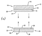
(1.二層接合方式I)
図1(a)を参照すると、前躯体構造体10が概略断面図として示されている。構造体10は第1の基板12を含む。基板12は前面又はデバイス面14、背面16、及び最外側エッジ18を有する。基板12は任意の形状でよいが、通常は円形形状である。好ましい第1の基板12はデバイスウェーハーを含み、そのデバイス面は集積回路、MEMS、マイクロセンサー、動力半導体、発光ダイオード、フォトニック回路、インタポーザー、埋込受動素子、及び、シリコン、又はシリコンゲルマニウム、ガリウムヒ素、およびガリウム窒素のような半導体材料上に製造される又はそれらから製造される他のマイクロデバイス、から成る群から選択されたデバイスアレイ(図示されていない)を含む。これらのデバイスの表面は一般に以下の材料の1つ以上から形成された構造体(これも図示されていない)を含む:シリコン、ポリシリコン、二酸化ケイ素、(オキシ)窒化ケイ素、金属(例えば、銅、アルミニウム、金、タングステン、タンタル)、低k誘電体、高分子誘電体、および各種窒化金属および金属シリサイド。またデバイス面14は、半田バンプ;金属ポスト;金属ピラー;及びシリコン、ポリシリコン、二酸化ケイ素、(オキシ)窒化ケイ素、金属、低k誘電体、ポリマー誘電体、窒化金属、及び金属シリサイドから成る群から選択される材料から形成される構造体:から成る群から選択される少なくとも1つの構造体を含むことができる。
(1. Two-layer bonding method I)
Referring to FIG. 1 (a), a
図1(a)に示すようにデバイス面14上に第1の接合層20を形成するように、第1の基板12に組成物が適用される。接合層20は第1の基板12から離れた上部表面21を有し、好ましくは、第1の接合層20はデバイス面14に直接隣接して形成される(即ち、第1の接合層20と基板12との間に中間層が存在しない)。組成物は任意の既知の方法によって適用することができる。1つの好ましい方法は、速度約500rpm〜約5,000rpm(好ましくは約500rpm〜約2,000rpm)で、時間約5秒〜約120秒(好ましくは約30秒〜約90秒)間、組成物をスピンコートすることである。組成物を適用した後、温度約80℃〜約250℃、より好ましくは約170℃〜約220℃で時間約60秒〜約8分(好ましくは約90秒〜約6分)間加熱することが好ましい。第1の接合層20を形成するために用いられる組成物に依存して、焼成によって架橋反応が開始され層20を硬化することができる。幾つかの実施形態では、用いられる組成物に応じて、層に多段焼成プロセスを施すことが好ましい。また幾つかの例では、組成物の更なるアリコットを用いて上述の適用及び焼成プロセスが繰り返され、多数のステップによって、第1の接合層20が第1の基板12上に「構築される」。
The composition is applied to the
第2の前駆体構造体22も図1(a)の概略断面図に示されている。第2の前駆体構造体22は第2の基板24を含む。この実施形態では、第2の基板24はキャリヤーウェーハーである。即ち、第2の基板24は前面又はキャリヤー面26、背面28、及び最外側エッジ30を有する。第2の基板24は任意の形状でよいが、通常は円形形状であり、第1の基板12と同じサイズである。好ましい第2の基板24はシリコン、サファイヤ、水晶、金属(例えば、アルミニウム、銅、鋼)、並びに種々のガラス及びセラミックスを含む。
The
図1(a)に示すように、キャリヤー面26上に第2の接合層32を形成するように、第2の組成物が第2の基板24に適用される。第2の接合層32は、第2の基板24から離れた上部表面33、及び第2の基板24に隣接する下部表面35を有する。好ましくは、第2の接合層32はキャリヤー面26に直接隣接して形成される(即ち、第2の接合層32と第2の基板24との間に中間層が存在しない)。組成物は任意の既知の適用方法によって適用してよく、1つの好ましい方法は、組成物を、速度約500rpm〜約5,000rpm(好ましくは約500rpm〜約2,000rpm)で、時間約5秒〜約120秒(好ましくは約30秒〜約90秒)間スピンコートすることである。組成物が適用された後、好ましくは、温度約80℃〜約250℃、より好ましくは約170℃〜約220℃へ、時間約60秒〜約8分(好ましくは約90秒〜約6分)間加熱される。第2の接合層32を形成するために使用される組成物に依存して、焼成によって架橋反応が開始され層32を硬化することができる。幾つかの実施形態では、使用される組成物に応じて、層に多段焼成プロセスを施すことが好ましい
As shown in FIG. 1 (a), the second composition is applied to the
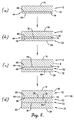
第1及び第2の接合層20及び32(並びに本明細書中に説明する他の層)の厚みは、図2を参照することによって最良に説明される。類似の番号が類似の部分を示すように用いられている。デバイス面14上に存在する上述のデバイスや、隆起した特徴、コンタクト孔、ビア孔、ライン、トレンチ等によるデバイス面14上のトポグラフィの変動を概略的に示すように、デバイス面14が図2に示されている。デバイス面14上に見られる様々な特徴の中に、最も高い特徴36及び最も低い特徴38がある(本明細書中に用いられる場合、「最も高い」は、特徴が第1の基板12の背面16から最も遠くまで延在している特徴を指し、一方「最も低い」は、その最下点が第1の基板12の背面に最も近い特徴を指す)。最も高い特徴36は最上表面36aを有し、一方最も低い特徴38は最下表面又は最下点38aを有する。トポグラフィが存在する(即ち、平面ではない) 表面に適用される層の厚みを指すときは、2つの厚みを参照としてもよい。T1は、図2に例示されるように最下表面又は最下点38aによって定義される下側平面40から上部表面21に延びる距離を示す。T2は最上表面36aの上で測定した層の厚みを示す。具体的には、図2に示すように、この厚みT2は上側表面42から始まり上部表面21まで延びる。平面の(又は実質的に平面の)表面に適用された層の厚みを指すときは、その厚みは図2のT3で表され、層32の下部表面35と上部表面33との間の距離である。最後に、幾つかの例では厚みT4が用いられ、これは下側平面40から上側表面42までの距離を示す。全ての厚みは5つの測定値の平均の厚みを示す。
The thickness of the first and second bonding layers 20 and 32 (and other layers described herein) is best described by referring to FIG. Similar numbers are used to indicate similar parts. The
本発明の実施形態において、第1の接合層20は、好ましくは厚みT1を有し、厚みT1は、少なくともT4に等しく、好ましくは約1.1T4〜約1.5T4、より好ましくは約1.2T4〜約1.3T4である。この結果、典型的には、厚みT1が、少なくとも約24μm、より好ましくは約45μm〜約200μm、更により好ましくは約50μm〜約150μmとなる。更に、第1の接合層20は好ましくは厚みT2を有し、厚みT2は約5μm以上、より好ましくは約5μm〜約50μm、更により好ましくは約10μm〜約30μmである。第2の接合層32は厚みT3を有し、厚みT3は約35μm未満、好ましくは約1μm〜約35μm、より好ましくは約1μm〜約25μm、更により好ましくは約1μm〜約15μmである。
In an embodiment of the present invention, the
第1の接合層20は好ましくは軟化点(環球式軟化点)を有し、その軟化点は第2の接合層32の軟化点より、約20℃以上高く、より好ましくは約20℃〜約200℃高く、更により好ましくは約20℃〜約100℃高い。この結果、典型的には、第1の接合層20の軟化点は約100℃以上、好ましくは約150℃〜約400℃、より好ましくは約200℃〜約300℃となる。更に、第2の接合層32の典型的な軟化点は、約220℃未満、好ましくは約50℃〜約220℃、より好ましくは約100℃〜約150℃となる。
The
第1及び第2の接合層20及び32が形成される材料は、第1及び第2の基板12及び24それぞれと並びに互いに強固な接着剤接合を形成できるものでなければならない。ASTMD4541/D7234の測定で、接着強さが約50psigより上、好ましくは約80psig〜約250psig、より好ましくは約100psig〜約150psigであるものが第1及び第2の接合層20及び32として使用するのに望ましい。
The material from which the first and second bonding layers 20 and 32 are formed must be capable of forming a strong adhesive bond with the first and
有利なことに、第1及び第2の接合層20及び32を形成するために用いる組成物は、上述の特性を有する層内に形成可能とされる市販の接合組成物から選択することができる。典型的には、そのような組成物は有機であり、溶媒系中に溶解又は分散されたポリマー又はオリゴマーを含む。ポリマー又はオリゴマーは、典型的には、環状オレフィン、エポキシ、アクリル、シリコン、スチレン、ハロゲン化ビニル、ビニルエステル、ポリアミド、ポリイミド、ポリスルホン、ポリエーテルスルホン、環状オレフィン、ポリオレフィンゴム、及びポリウレタン、エチレンプロピレンゴム、ポリアミドエステル、ポリイミドエステル、ポリアセタール、及びポリビニルブテロールの、ポリマー又はオリゴマーから成る群から選択される。典型的な溶媒系はポリマー又はオリゴマーの選択に依存する。組成物の総重量を100重量%としたときに、組成物の典型的な固形分は、約1重量%〜約60重量%、好ましくは約3重量%〜約40重量%の範囲となる。幾つかの適切な組成物が、各々参照として本明細書中に含まれる、米国特許公開番号第2007/0185310号、第2008/0173970号、第2009/0038750号、及び2010/0112305号に記載されている。 Advantageously, the composition used to form the first and second bonding layers 20 and 32 can be selected from commercially available bonding compositions that can be formed in a layer having the properties described above. . Typically such compositions are organic and comprise a polymer or oligomer dissolved or dispersed in a solvent system. The polymer or oligomer is typically a cyclic olefin, epoxy, acrylic, silicon, styrene, vinyl halide, vinyl ester, polyamide, polyimide, polysulfone, polyethersulfone, cyclic olefin, polyolefin rubber, and polyurethane, ethylene propylene rubber. , Polyamide ester, polyimide ester, polyacetal, and polyvinyl buterol are selected from the group consisting of polymers or oligomers. Typical solvent systems depend on the choice of polymer or oligomer. When the total weight of the composition is 100% by weight, the typical solid content of the composition ranges from about 1% to about 60% by weight, preferably from about 3% to about 40% by weight. Several suitable compositions are described in US Patent Publication Nos. 2007/0185310, 2008/0173970, 2009/0038750, and 2010/0112305, each of which is incorporated herein by reference. ing.
次に構造体10及び22は、第1の接合層20の上部表面21が第2の接合層32の上部表面33に接触するように向かい合わせにされ一緒にプレスされる(図1(b))。プレスされると同時に、十分な時間十分な圧力及び熱が加えられて、これら2つの構造体10及び22の接合が有効になり接合されたスタック34が形成される。接合パラメータは、接合層20及び32が形成される組成物に依存して変動するが、このステップの典型的な温度範囲は、約150℃〜約375℃の範囲、好ましくは約160℃〜約350℃の範囲であり、典型的な圧力範囲は、約1,000N〜約5,000N、好ましくは約2,000N〜約4,000Nであり、時間は約30秒〜約5分、より好ましくは約2分〜約4分である。
Next, the
この段階で、第1の基板12は安全にハンドリングすることができ、第2の基板24に接合されていなければ第1の基板に損傷を与え損ねなかった更なる処理を施すことができる。このように、基板12及び24の分離を起こすことなく構造体に、背面研削、CMP、エッチング、金属及び誘電体堆積、パターニング(例えば、フォトリソグラフィ、ビアエッチング)、不動態化、アニーリング、及びそれらの組合せ等の背面処理を安全に施すことができ、またこれらの後処理ステップ中に遭遇する任意の化学薬品が浸入することもない。第1の接合層20及び第2の接合層32は、これらのプロセスに耐えられるだけでなく、最大約450℃、好ましくは約200℃〜約400℃、より好ましくは約200℃〜約350℃の処理温度にも耐えうる。
At this stage, the
処理が完了すると、基板12及び24は、多くの分離方法(図示せず)によって分離することができる。1つの方法では第1及び第2の接合層20、32の1つ又は両方を溶媒(例えば、リモネン、ドデセン、プロピレングリコールモノエチルエーテル(PGME))中に溶解する。或いは、最初にレーザ切断、プラズマエッチング、ウォータージェッティング、又は、第1及び第2の接合層20、32を効果的にエッチング又は分解するその他の高エネルギー技術を用いて第1及び第2の接合層20、32の1つ又は両方の周囲を機械的に分解又は破壊することによって基板12及び24を分離することができる。また、最初に第1及び第2の接合層20、32を貫通して鋸引き又は切断するかもしくは層20、32を何らかの同等手段を用いて切り裂くことも適切である。上述の手段のどれを用いるかに拘らず、その後、低機械力(例えば、指の圧力、緩やかな割り裂き)を加えることにより基板12及び24を完全に分離させることができる。
When processing is complete, the
最も好ましい分離方法は、接合されたスタック34を、約100℃以上、好ましくは約150℃〜約220℃、より好ましくは約180℃〜約200℃の温度に加熱することである。これらの温度で、第2の接合層32が軟化し、基板12及び24を分離させる(例えば、参照として本明細書に含まれる、米国特許公開番号第2008/0200011号に記載されるようなスライド剥離方法によって)ことは理解されるであろう。分離後、残留する第1又は第2の接合層20及び32を、特定の層20又は32を溶解する性能のある溶媒を用いて除去することができる。幾つかの実施形態では、第1の接合層20を形成するための組成物は、その一部又は全部が第1の基板12上に永久的に残ることが適切であるように選択される。その場合、第1の接合層20が後続のウェーハー処理ステップにおいて何らかの機能(例えば、間隙充填)を実行する。これは先行技術のプロセスにはなかった有利な点である。
The most preferred separation method is to heat the bonded
この二層の実施形態が多くの利点を提供することは理解されるであろう。本発明の方法により、構造体の接合温度及び全体の熱安定性を制御することができる。即ち、本発明の方法は、より高い処理温度の使用を可能にすると同時により低い温度で接合及び剥離を可能にする。 It will be appreciated that this bi-layer embodiment offers many advantages. By the method of the present invention, the bonding temperature and the overall thermal stability of the structure can be controlled. That is, the method of the present invention allows the use of higher processing temperatures while simultaneously allowing bonding and debonding at lower temperatures.
(2.二層接合方式II)
第2の二層接合方式を図3に示す。類似の番号は類似の部分を表す。この実施形態では、上部表面46及び下部表面48を有する「クリーニング層」又はリフトオフ層44がデバイス面14上に形成される。リフトオフ層44は、任意の既知の適用方法によって形成することができ、1つの好ましい方法では、層44を形成するために用いられる組成物を、速度約500rpm〜約5,000rpm(好ましくは約500rpm〜約2,000rpm)で、時間約5秒〜約120秒(好ましくは約30秒〜約90秒)の間、スピンコートする。組成物は、適用された後、好ましくは、温度約60℃〜約250℃、より好ましくは約80℃〜約220℃に、時間約60秒〜約4分(好ましくは約90秒〜約2分)間、加熱される。幾つかの実施形態では、使用される組成物に応じて、層に多段焼成プロセスを施すことが好ましい。リフトオフ層44を形成するために用いられる組成物に依存して、焼成によって架橋反応が開始され層44を硬化することができる。
(2. Two-layer bonding method II)
A second two-layer bonding method is shown in FIG. Similar numbers represent similar parts. In this embodiment, a “cleaning layer” or lift-
リフトオフ層44は好ましくは厚みT1を有し、厚みT1は約3μm未満、より好ましくは約0.5μm〜約3μm、更により好ましくは約1μm〜約1.5μmである。別の実施形態では、リフトオフ層44が共形層であり、 そのため上述の厚みを有しない。
リフトオフ層44を形成するために用いられる組成物は、1%の塩化水素酸水溶液、50%の酢酸水溶液、イソプロパノール、1−ドデセン、R−リモネン、シクロペンタノン、PGME、及びテトラメチルアンモニウム水酸化物(TMAH)から成る群から選択される溶液中で層44が可溶性であるように選択されるべきである。より詳細には、リフトオフ層44は、特定の除去溶液に接触してから約4〜5時間の後に、約95%以上、好ましくは約99%以上、好ましくは100%溶解/除去される。
The composition used to form the lift-
リフトオフ層44を形成するために好ましい組成物は上述の特性を持つ市販の組成物から選択することができる。そのような組成物の例には、ポリ(ビニルピリジン)及びポリアミド酸から成る群から選択される組成物が含まれる。これら2種の好ましい組成物は、ProLIFT(R)及び、湿式現像可能な材料のWGFシリーズ(Brewer Science社から入手可能)である。使用が特に好ましい組成物は参照として本明細書に含まれる、米国特許公開番号第2009/0035590号に記載されている。
A preferred composition for forming the lift-
次にリフトオフ層44上に接合層20が形成される(図3(b))。接合層20は、好ましくは、図1に関連して説明したような厚みT1、及び、約5μm以上、より好ましくは約5μm〜約50μm、更により好ましくは約10μm〜約30μmの厚みT2を有する。次に第2の基板24が上述のように接合層20に接合され(図3(c))、接合されたスタック50を形成する。次に接合されたスタック50に上述のような更なる処理を施すことができる。
Next, the
第1及び第2の基板12及び24の分離の準備が整うと、接合されたスタック50は、上述の除去溶液の1つに暴露され(好ましくは約1分〜約5時間、より好ましくは約2分〜約60分の間)、その結果、溶液がリフトオフ層44を溶解して、基板12及び24が分離される。有利なこととして、リフトオフ層44が「クリーニング」層として機能する実施形態では、基板12及び24を分離させるために十分に接合層20を軟化させるよう加熱することによって基板12及び24を分離させることができる。基板12及び24が分離されると、リフトオフ/クリーニング層44を除去溶液によって除去することができ、これは同時に残っているすべての接合層20残留物も除去する。
When the first and
(3.三層接合方式I)
第1の三層接合方式が図4に示される。類似の番号は類似の部分を表す。図4に示される実施形態は、図3に示されるものと類似しているが、図3の第1の接合層20が第2の接合層32に変わり、「クリーニング」又はリフトオフ層44と第2の接合層32との間に付加的な層が追加されているところが異なっている。詳細には、リフトオフ層44がデバイス面14上に形成された後(上述したように、及び図4(a)参照)、上部表面54及び下部表面56を有する剛性層52がリフトオフ層44の上部表面46上に形成される(図4(b))。本明細書中に用いられる場合「剛性」はレオメータの測定で1GPa以上の高い剛性率を指す。更に、「剛性」は、処理温度(典型的には約150℃〜約400℃、好ましくは約200℃〜約300℃)で流動することのない層を指す。
(3. Three-layer joining method I)
A first three-layer joining scheme is shown in FIG. Similar numbers represent similar parts. The embodiment shown in FIG. 4 is similar to that shown in FIG. 3 except that the
剛性層52を形成するために用いられる組成物は、第1の接合層20に関して上述した組成物と同じ種類である。更に、剛性層52は第1の接合層20に関して上述したものと同様の方法で形成される(リフトオフ層44が事実上共形である場合は、図1に関して説明されたものと同様の厚みを含む)。剛性層52は(リフトオフ層44が事実上共形でない場合)好ましくは約1μm〜約35μm、より好ましくは約1μm〜約25μm、更により好ましくは約1μm〜約15μmの厚みT3を有する。
The composition used to form the
図4(c)を参照すると、第2の接合層32が剛性層52の上部表面54上に、既に説明したものと同様の適用方法及び組成物の種類を用いて形成される。この実施形態では、第2の接合層32の厚みT3は、約1μm〜約35μm、より好ましくは約1μm〜約25μm、更により好ましくは約1μm〜約15μmである。
Referring to FIG. 4 (c), the
剛性層52は、好ましくは第2の接合層32の軟化点よりも、約20℃以上高い、より好ましくは約20℃〜約300℃高い、更により好ましくは約20℃〜約100℃高い軟化点を有する。この結果、典型的には、剛性層52の軟化点は、約100℃以上、好ましくは約150℃〜約400℃、より好ましくは約200℃〜約300℃となる。
The
第2の基板24は上述のように接合層32に接合され、接合されたスタック58を形成する(図4(d))。次に接合されたスタック58に上述のような更なる処理を施すことができる。第1及び第2の基板12及び24の分離の準備が整うと、接合されたスタック58は上述の除去溶液の1つに暴露され、その結果、溶液がリフトオフ層44を溶解して、基板12及び24を分離させる。或いは、上述のようにスタック58を加熱して接合層32を軟化させることよって分離を起こすこともできる。後者の例では、リフトオフ層44がここでもクリーニング層として機能し、層44を除去溶液によって除去することによって接合層の残留物も除去することができる。
The
(4.三層接合方式II)
もう1つの三層接合方式が図5(a)〜5(d)に示される。類似の番号は類似の部分を表す。この実施形態は上述の実施形態の変形であり、ここでは多層接合システムは2つの剛性層52を含み、その2つの層52の間に第2の接合層32の層が存在する。組成物選択、処理パラメータ及びステップ等は対応する層に関して上述したものと同様である。図示されていないが、剛性層52の1つ(好ましくは第2の基板24に一番近い剛性層52)と接合層32を入れ換えることによって、この実施形態を変形することができる。
(4. Three-layer bonding method II)
Another three-layer bonding method is shown in FIGS. 5 (a) to 5 (d). Similar numbers represent similar parts. This embodiment is a variation of the above-described embodiment, in which the multi-layer bonding system includes two
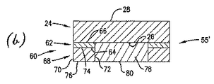
(5.基板エッジにおける多重層)
本発明の更なる実施形態が、図6及び図7に図示されている。類似の部分は類似の様式で番号が付されている。これらの実施形態については、参照として本明細書中に含まれる、米国特許公開番号第2009/0218560号を参照されたい。
(5. Multiple layers at the substrate edge)
A further embodiment of the present invention is illustrated in FIGS. Similar parts are numbered in a similar fashion. For these embodiments, see US Patent Publication No. 2009/0218560, which is incorporated herein by reference.
図6(a)を参照すると、この実施形態では、構造体55が描かれている。第1の基板12のデバイス面14は、周縁域57、中央域59、及び、周縁域57での二層接合システム60を含む。システム60は、上部表面64及び下部表面66、並びに接合部(以下接合セグメントという)68を有する薄層62を含む。接合セグメント68は、外側表面70、内側表面72、下部表面74、及び接合表面76を含む。薄層62の下部表面66は、周縁域57で第1の基板12のデバイス面14に隣接し、一方、接合セグメント68の下部表面74は薄層62に隣接する。
Referring to FIG. 6A, in this embodiment, the
薄層62はリフトオフ層44に関して上述したものと同様のリフトオフ層であってよく、或いは薄層62は接着増進剤層であってよい。それが接着増進剤層である例では、任意の市販の接着増進剤組成物をこの用途に用いることができる。このような組成物の幾つかの例には、有機シラン(例えば、ProTEK(R)プライマー、Brewer Science社から入手可能)が含まれる。
The
スピンコートの後に特定の組成物に最適な温度で焼成を行う等の従来の方法で薄層62を形成することができる。例えば、上述のようにリフトオフ層44を形成するために従う方法を、薄層62の形成に用いてもよい。また、図6(a)は、この層が周縁域57にのみ存在するように描いているが、薄層62は中央域59にも存在するようにデバイス面14全体に亘って延在してもよい。薄層62は好ましくは周縁域57において、約1μm〜約35μm、より好ましくは約1μm〜約25μm、更により好ましくは約1μm〜約15μmの厚みT3を有する。薄層62がデバイス面14全体に亘って延在する例では、その厚みT1は、約0.1μm〜約20μm、好ましくは約0.25μm〜約10μm、より好ましくは約1μm〜約3μmとなる。他の例では、薄層62を共形層とすることができ、その場合は上述の厚みを有しない。
The
接合セグメント68は、第1及び第2の接合層20及び32に関して上述したものを含む任意の市販の接合組成物から形成することができる。接合セグメント68は、典型的には約2mm〜約15mm、好ましくは約2mm〜約10mm、より好ましくは約2mm〜約5mmの幅「D」を有する。更に、接合セグメント68は、好ましくは約5pm〜約100μm、より好ましくは約5μm〜約50μm、更により好ましくは約10μm〜約30μmの厚みT3を有する。
The
この時点で、上述の実施形態で説明したように、構造体55を第2の基板24に接合することができ、又は、図6(b)に示すようにデバイス面14の中央域59に充填層78を形成することができる。充填層78は、接合セグメント68に関して上述したものと同様の厚みを有する。充填層78は、典型的には、溶媒系中に分散又は分解されたモノマー、オリゴマー、及び/又はポリマーを含む材料から形成される。充填層78がスピンコートを介して適用される場合は、この材料の固形分は約1重量%〜約50重量%、、より好ましくは約5重量%〜約40重量%、更により好ましくは約10重量%〜約30重量%であることが好ましい。最適なモノマー、オリゴマー、及び/又はポリマーの例には、環状オレフィンポリマーおよびコポリマーならびに原子状フッ素含有量が高い(重量で約30%超)フッ化シロキサンポリマーのような非晶形フルオロポリマー、フッ化エチレン−プロピレンコポリマー、ペンダントペルフルオロアルコキシ基を持つポリマー、及びテトラフルオロエチレンのコポリマーから成る群から選択されるものが含まれ、なかでも2,2−ビス−トリフルオロメチル−4,5−ジフルオロ−l,3−ジオキソールのコポリマーがとりわけ好まれる。これらの材料の接合強度は、それらの特定の化学構造体、及び適用時に用いられるコーティング及び焼成条件に依存することが理解されるであろう。
At this point, the
この実施態様において、充填層78は強い接着接合を形成しないことが好ましく、これにより後の分離が容易になる。一般論として、非晶形高分子材料で:(1)表面自由エネルギーが低く;(2)不粘着性でガラス、シリコン、および金属面に強くは接着しないことが知られ(すなわち、一般に水酸基またはカルボン酸基の濃度が非常に低いか、好ましくはそのような基が全くない);(3)溶液から流し込めるかまたはラミネート用に薄いフィルムに形成でき;(4)代表的な接合条件の下で流れ、デバイスウェーハー面のトポロジーを充填し、基板間に気泡の無い接合線を形成し;かつ(5)背面処理工程中に、例え高温または高真空条件下で実施されたとしても、遭遇する機械的応力の下で割れず、流れず、または再配分しない、ものが望ましい。本明細書に用いる場合、低い表面自由エネルギーとは接触角測定により判定される水との接触角が少なくとも約90°および臨界表面張力が約40ダイン/cm未満、好ましくは約30ダイン/cm未満、より好ましくは約12ダイン/cm〜約25ダイン/cm、を示す高分子材料と定義される。
In this embodiment, the
低い接合強度とはベタ付かず又は接着剤付の便箋を剥がすのに用いる程度の軽い手の圧力だけで基板から剥がせるポリマー材料を指している。従って、約50psig未満、好ましくは約35psig未満、より好ましくは約1psig〜約30psigの接着強度を有する任意のものが充填層22として用いるのに望ましい。上述の特性を示す適切なポリマー材料の例には、Mitsui社のAPEL(R)、Ticona社のTOPAS(R)、及びZeon brands社のZEONOR(R)として販売されている幾つかの環状オレフィンポリマー及びコポリマー及び、アサヒガラス社販売のCYTOP(R)ポリマー及びDuPont社販売のTEFLON(R)AFポリマー等の溶媒可溶性のフルオロポリマーが含まれる。これらの材料の接合強度は、それらを適用する際に用いられるコーティング及び焼成条件に依存する。
Low bond strength refers to a polymer material that can be peeled off from a substrate with only light hand pressure that is not sticky or that can be used to peel off adhesive notes. Accordingly, any having an adhesive strength of less than about 50 psig, preferably less than about 35 psig, more preferably from about 1 psig to about 30 psig is desirable for use as the
この時点で、上記の実施形態で説明されたステップを用いて第2の基板を構造体55に接合して、図6(c)に示すように接合されたスタック82を形成することができる。スタック82上での所望の処理が完了した後、第1の基板12及び第2の基板24は直ちに分離することができる。1つの分離方法では、最初に接合セグメント68を、溶媒又は他の化学剤の助けを得て溶解する。これは溶媒内に浸漬するか、又はこれを溶解するために溶媒のジェットを接合セグメント68にスプレーすることによって果たせる。接合セグメント68を破壊するために溶媒溶解が用いられる場合、熱可塑性材料の使用が特に望ましいものである。この除去プロセス中に典型的に用いられる溶媒は、乳酸エチル、シクロヘキサノン、−メチルピロリドン、脂肪族溶媒(例えば、ヘキサン、デカン、ドデカン、及びドデセン)、及びそれらの混合物から成る群から選択されるものを含む。
At this point, the second substrate can be bonded to the
更に基板12及び24は最初にレーザ切断、プラズマエッチング、ウォータージェッティング、又は接合セグメント68を効果的にエッチング又は分解する他の高エネルギー技術を用いて、接合セグメント68の連続性を機械的に分解又は破壊することによっても分離できる。また、最初に接合セグメント68を貫通して鋸引き又は切断するかもしくは接合セグメント68を何らかの同等手段を用いて切り裂くことも適切である。
In addition, the
上述の手段のどれを用いるかに拘らず、その後、低機械力(例えば、指の圧力、緩やかな割り裂き)を加えてに基板12及び24を完全に分離させることができる。有利な点として分離のために充填層78と基板12又は24との間の強固な接着剤接合を克服する必要がない。その代わりに分離を起こさせるために、周縁域57内の接合セグメント68の接着剤接合を剥離する必要があるだけである。必要に応じてその後残留するすべての材料を除去するために適切な溶媒を用いて基板12及び/又は24の表面をきれいにすすぐ。
Regardless of which of the above means is used, the
なお、上の実施形態に関して、充填層78の形成の前に接合セグメント68を形成するという順は1つの可能性として挙げただけであり、最初に充填層78を形成し、その後接合システム60又は接合セグメント68を形成することも可能である。形成の順番は、本発明にとって重要ではなく当業者であれば変更することができる。
It should be noted that with respect to the above embodiment, the order of forming the joining
図7を参照すると、本発明の更なる実施形態が示される。類似の番号は類似の部分を表す。この実施形態は、図6に類似しているが、第1及び第2の基板12及び24が入れ替わっているところが異なる。即ち、薄層62が第1の基板12のデバイス面14ではなく第2の基板24のキャリヤー面26に接触し、接合セグメント68の接合表面76が第1の基板12のデバイス面14に接合されている。このように、特定の用途の必要性に依存して、薄層62は接合セグメント68の下部表面74又は接合表面76、或いは両方に隣接することができる。この実施形態では、薄層62は図6の実施形態に関して説明した厚みT3を有し、また、これらの厚みは薄層62全体に亘って同様である。
Referring to FIG. 7, a further embodiment of the present invention is shown. Similar numbers represent similar parts. This embodiment is similar to FIG. 6 except that the first and
(6.基板エッジにゾーン領域を備える多重層)
図8は、本発明の更なる実施形態を示す。類似の番号は類似の部分を表す。図8(a)を参照すると、第2の接合層32が、第1の基板12の周縁域57のみにおいて形成される。適用方法、所望の特性(軟化点を含む)、及び第2の接合層32として用いられる可能性のある組成物は既に説明したとおりである。図8(b)を参照すると、上の図6及び図7に関して説明したように充填層78がデバイス面14の中央域59に形成される。
(6. Multilayer with zone area at substrate edge)
FIG. 8 shows a further embodiment of the present invention. Similar numbers represent similar parts. Referring to FIG. 8A, the
次に、図8(c)に示すように、第1の接合層20が第2の接合層32の上部表面33上、及び充填層78の上部表面80上に形成され構造体84を形成する。同様に、適用方法、所望の特性、及び第1の接合層20として用いる可能性のある組成物は既に説明したとおりである。第2の基板24は構造体84に先の実施形態で説明したステップを用いて接合することができ、図8(d)に示すように接合されたスタック86を形成する(或いは、実施例18で説明したように、代わりに第2の基板24のキャリヤー面21上に第1の接合層20を形成して次に2つの構造体を共にプレスして、図1に示すステップの順番と同様に接合されたスタック86を形成する。)。
Next, as shown in FIG. 8C, the
次いで接合されたスタック86に上述のような更なる処理を施すことができる。第1及び第2の基板12及び24の分離の準備が整うと、接合されたスタック86は、除去溶液(例えば、リモネン、ドデセン、PGME)に暴露され、その結果、溶液が第2の接合層32を溶解して、それによって基板12及び24が分離できる。或いはスタック86を加熱して、第1の接合層20よりも低い軟化点を有する第2の接合層32を軟化させ、それによって上述のように基板12及び24を分離可能にすることによって分離を起こすこともできる。
The bonded
図9を参照すると、本発明の更なる実施形態が示される。類似の番号は類似の部分を表す。この実施形態は、図8に類似しているが、第1及び第2の基板12及び24が入れ替えられているところが異なる。即ち、第2の接合層32及び充填層78が、第1の基板12のデバイス面14ではなく、第2の基板24のキャリヤー面26に接触し、第1の接合層20は、第1の基板12のデバイス面14に接合される。このように、特定の用途の必要性に依存して、第2の接合層32及び充填層78の位置を調整することができる。
Referring to FIG. 9, a further embodiment of the present invention is shown. Similar numbers represent similar parts. This embodiment is similar to FIG. 8 except that the first and
特定の基板表面を、実質的に又は完全に覆うための種々の接合層、リフトオフ層、及び剛性層が示されている、上記の接合方式のそれぞれに関して、これらの層の1つ又は複数を(たとえ、図示されていなくても)特定の基板の一部のみを覆うように変更できることが理解されるであろう。即ち、特定の基板表面の一部分のみをその特定の層に接触させることもでき、これも本発明の範囲内である。 For each of the above bonding schemes, various bonding layers, lift-off layers, and rigid layers are shown to substantially or completely cover a particular substrate surface, one or more of these layers ( It will be understood that it can be modified to cover only a portion of a particular substrate (even if not shown). That is, only a portion of a particular substrate surface can be contacted with that particular layer, which is also within the scope of the present invention.
更に、たとえ層が第1の基板(デバイス)上に積み重ねて形成され、その後、第2の基板(キャリヤー)と接合されている例においても、その代わりに全ての層を第2の基板の上に積み重ねて形成し、次に第1の基板と接合されることもできる。或いは、1つ又は複数の層を第1の基板上に形成し、一方、別の層を第2の基板上に形成し、次に2つの基板を共に接合してもよい。結果の構造体が本明細書中で図示及び/又は説明した層システムを有している限り、順番は重要ではない。 Furthermore, even in the example where the layers are stacked on the first substrate (device) and then bonded to the second substrate (carrier), all layers are instead deposited on the second substrate. Can be stacked and then bonded to the first substrate. Alternatively, one or more layers may be formed on a first substrate while another layer is formed on a second substrate and then the two substrates are bonded together. As long as the resulting structure has the layer system shown and / or described herein, the order is not important.
以下の実施例は、本発明に係る好ましい方法を説明する。しかしながら、これらの実施例は例示のために提供されるものであり本発明の全体の範囲を制限するものではないことを理解すべきである。 The following examples illustrate preferred methods according to the present invention. However, it should be understood that these examples are provided by way of illustration and do not limit the overall scope of the invention.
実施例1から9は本発明の改善された接合性能を説明する。実施例l0から16は剥離後にクリーニングされる接合組成物の改善された性能を説明する。 Examples 1 to 9 illustrate the improved bonding performance of the present invention. Examples 10 to 16 illustrate the improved performance of bonding compositions that are cleaned after stripping.
(実施例1)
(環状オレフィンコポリマー(COC)接合組成物Aの組成)
この調製において、250グラムのエテンノルボルネンコポリマー(APL8008T、三井化学アメリカ社、ニューヨーク州ライブルック、から取得)及び3.125グラムのフェノール系酸化防止剤(IRGANOX1010、BASF社、ドイツ、から取得)を373.45グラムのR−リモネン(Florida Chemical社、フロリダ州ウィンターヘブン、から取得)及び373.45グラムのシクロオクタン(Sigma−Aldrich社、ミズーリ州セントルイス、から取得)中に溶解した。全ての成分が溶解するまで混合物を室温で攪拌させた。最終溶液は、25.31%の固形物を有した。
Example 1
(Composition of cyclic olefin copolymer (COC) bonding composition A)
In this preparation, 250 grams of ethene norbornene copolymer (obtained from APL8008T, Mitsui Chemicals America, Live Look, NY) and 3.125 grams of phenolic antioxidant (IRGANOX 1010, BASF, Germany, acquired) 373 Dissolved in .45 grams of R-limonene (obtained from Florida Chemical, Winter Haven, FL) and 373.45 grams of cyclooctane (obtained from Sigma-Aldrich, St. Louis, MO). The mixture was allowed to stir at room temperature until all components were dissolved. The final solution had 25.31% solids.
(実施例2)
(COC接合組成物Bの組成)
この調製において、210.31グラムのエタンノルボルネンコポリマー(Topas8007、Topas Advanced Polymers社、ケンタッキー州フローレンス、から取得)及び62.4グラムの低分子量COCポリマー(Topas TM、Topas Advanced Polymers社、ケンタッキー州フローレンス、から取得)を4.0グラムのフェノール系酸化防止剤(Irganox1010)を含む、706グラムのR−lリモネン、及び分子量2、800ダルトンの14.5グラムのポリイソブチレン(Scientific Polymer Products社、ニューヨーク州オンタリオ、から取得)中に溶解した。全ての成分が溶解するまで混合物を室温で攪拌させた。溶液は、29%の固形分を有した。
(Example 2)
(Composition of COC bonding composition B)
In this preparation, 210.31 grams of ethane norbornene copolymer (obtained from Topas 8007, Topas Advanced Polymers, Florence, Ky.) And 62.4 grams of low molecular weight COC polymer (Topas ™, Topas Advanced Polymers, Kentucky, Kentucky). 706 grams of R-l limonene, containing 4.0 grams of phenolic antioxidant (Irganox 1010), and 14.5 grams of polyisobutylene with a molecular weight of 2,800 Dalton (Scientific Polymer Products, NY) Dissolved in Ontario, acquired). The mixture was allowed to stir at room temperature until all components were dissolved. The solution had a solid content of 29%.
(実施例3)
(COC接合組成物Cの組成)
この調製において、50グラムの実施例2からのCOC接合組成物Bを、50グラムのR−リモネンと混合した。混合物を室温で攪拌させ溶液を形成した。溶液は14.5%の固形物を有した。
(Example 3)
(Composition of COC bonding composition C)
In this preparation, 50 grams of COC bonding composition B from Example 2 was mixed with 50 grams of R-limonene. The mixture was allowed to stir at room temperature to form a solution. The solution had 14.5% solids.
(実施例4)
(接合組成物Dの組成)
この調製において、120グラムのWaferBOND(R)HT−10.10材料(Brewer Science社から取得)を、80グラムの1−ドデセン(Sigma−Aldrich社、ミズーリ州セントルイス)と混合した。混合物を室温で攪拌させ溶液を形成した。
Example 4
(Composition of bonding composition D)
In this preparation, 120 grams of WaferBOND (R) HT-10.10 material (obtained from Brewer Science, Inc.), 80g of 1-dodecene (Sigma-Aldrich, Inc., St. Louis, MO) was mixed with. The mixture was allowed to stir at room temperature to form a solution.
(実施例5)
(デバイスウェーハー上の厚COC接合組成物A層、及びキャリヤーウェーハー上の薄COC接合組成物C層)
この手順では、コーティングされた基板と第2の基板との間の効果的な接合を得るために270℃で十分に流動するように設計された環状オレフィンポリマーコーティング層である実施例1からのCOC接合組成物A、10mLを200mmのシリコンウェーハー上にスピンコートし、(後述するスピン及び焼成パラメータを用いて)焼成し、COC接合組成物Aの膜を形成した。実施例1からの10mLのCOC接合組成物Aの第2のアリコットを用いて、このプロセスを正確に繰り返した。この第2のアリコットは第1の膜の上に更に膜を形成するために用いられた。両方の適用ステップの後の最終の膜厚は96μmであった。
(Example 5)
(Thick COC bonding composition A layer on device wafer and thin COC bonding composition C layer on carrier wafer)
In this procedure, the COC from Example 1, which is a cyclic olefin polymer coating layer designed to flow sufficiently at 270 ° C. to obtain an effective bond between the coated substrate and the second substrate. The bonding composition A, 10 mL, was spin-coated on a 200 mm silicon wafer and baked (using the spin and baking parameters described below) to form a COC bonding composition A film. This process was exactly repeated using a second aliquot of 10 mL COC bonding composition A from Example 1. This second aliquot was used to form an additional film on the first film. The final film thickness after both application steps was 96 μm.
コーティングされた基板と第2の基板との間の効果的な接合を得るために220℃で十分に流動するように設計された環状オレフィンポリマーコーティング層である実施例3からのCOC接合組成物Cを別の200mmシリコンウェーハー上にスピンコートした。COC接合組成物Cの厚みは約3μmであった。スピンコート及び焼成パラメータはCOC接合組成物A及びCOC接合組成物Cのためのものと同一であり、以下の通りであった。
スピンコート条件:800rpmのスピンコートを60秒間、加速は10、000rpm/秒
焼成条件、記載順:80℃で2分、110℃で2分、160℃で2分、及び220℃で6分
COC bonding composition C from Example 3, which is a cyclic olefin polymer coating layer designed to flow sufficiently at 220 ° C. to obtain an effective bond between the coated substrate and the second substrate. Was spin coated onto another 200 mm silicon wafer. The thickness of the COC bonding composition C was about 3 μm. The spin coating and firing parameters were the same as for COC bonding composition A and COC bonding composition C and were as follows.
Spin coating conditions: 800 rpm spin coating for 60 seconds, acceleration is 10,000 rpm / sec Firing conditions, listed in order: 80 ° C. for 2 minutes, 110 ° C. for 2 minutes, 160 ° C. for 2 minutes, and 220 ° C. for 6 minutes
上述のように、COC接合組成物A及びCOC接合組成物Cでコーティングされた2つのシリコンウェーハーを、5、800Nの接合圧力の圧力チャンバ内の加熱真空内で、220℃で3分間真空下で向かい合わせで接合した。次に、参照として本明細書に含まれる米国特許公開番号第2010/0206479号(Brewer Science社、ミズーリ州ローラ、から取得)に記載の方法と同様のスライドプロセスを用いる、剥離装置(デボンダー)で、接合されたウェーハーを220℃で分離した。 As described above, two silicon wafers coated with COC bonding composition A and COC bonding composition C were heated under vacuum at 220 ° C. for 3 minutes in a heating vacuum in a pressure chamber at a bonding pressure of 5,800 N. Joined face to face. Next, in a peeling apparatus (debonder) using a sliding process similar to that described in US Patent Publication No. 2010/0206479 (obtained from Brewer Science, Roller, Missouri), incorporated herein by reference. The bonded wafers were separated at 220 ° C.
(実施例6)
(厚COC接合組成物A及び薄COC接合組成物C)
この手順では、コーティングされた基板と第2の基板との間の効果的な接合を得るために、270℃で十分に流動するように設計された環状オレフィンポリマーコーティング層である実施例1からのCOC接合組成物A、10mLを、200mmのシリコンウェーハー上にスピンコートし、焼成し(後で説明するスピン及び焼成パラメータを用いて)COC接合組成物Aの膜を形成した。実施例1からの10mLのCOC接合組成物Aの第2のアリコットを用いて、このプロセスを正確に繰り返した。この第2のアリコットは、第1の膜の上に更に膜を形成するために用いられた。両方の適用ステップの後の最終の膜厚は93μmであった。
(Example 6)
(Thick COC bonding composition A and thin COC bonding composition C)
This procedure from Example 1 is a cyclic olefin polymer coating layer designed to flow sufficiently at 270 ° C. to obtain an effective bond between the coated substrate and the second substrate. COC bonding composition A, 10 mL, was spin-coated on a 200 mm silicon wafer and baked (using the spin and baking parameters described later) to form a film of COC bonding composition A. This process was exactly repeated using a second aliquot of 10 mL COC bonding composition A from Example 1. This second aliquot was used to form an additional film over the first film. The final film thickness after both application steps was 93 μm.
コーティングされた基板と第2の基板との間の効果的な接合を得るために、220℃で十分に流動するように設計された環状オレフィンポリマーコーティング層である実施例3からのCOC接合組成物CをCOC接合組成物A膜の上に更にスピンコートした。COC接合組成物Cの厚みは約8μmであった。スピンコート及び焼成パラメータはCOC接合組成物AのためのものとCOC接合組成物Cのためのものは同一であり、以下の通りであった。
スピンコート条件:800rpmのスピンコートを60秒間、加速は10、000rpm/秒
焼成条件、記載順:110℃で4分、160℃で2分、及び220℃で6分
COC bonding composition from Example 3 which is a cyclic olefin polymer coating layer designed to flow sufficiently at 220 ° C. to obtain an effective bond between the coated substrate and the second substrate C was further spin coated on the COC bonding composition A film. The thickness of the COC bonding composition C was about 8 μm. The spin coating and firing parameters for COC bonding composition A and COC bonding composition C were the same and were as follows.
Spin coating conditions: 800 rpm spin coating for 60 seconds, acceleration is 10,000 rpm / second Firing conditions, listed in order: 110 ° C. for 4 minutes, 160 ° C. for 2 minutes, and 220 ° C. for 6 minutes
別の200mmシリコンウェーハーの中心をフッ化シラン(ヘプタデカフルオロ−1、1、2、2−テトラヒドロデシルトリクロロシラン)でコーティングし、一方、ウェーハーの外側エッジに沿った3mmの領域はフッ化シランがないままにした。フッ化シランをコーティングするための詳細なプロセスは、参照として本明細書に含まれる、米国特許公開番号第2009/10218560号の実施例1に記載されている。 The center of another 200 mm silicon wafer was coated with fluorinated silane (heptadecafluoro-1,1,2,2-tetrahydrodecyltrichlorosilane), while the 3 mm area along the outer edge of the wafer was fluorinated with silane Left unattended. The detailed process for coating the fluorinated silane is described in Example 1 of US Patent Publication No. 2009/10218560, which is incorporated herein by reference.
上述のウェーハー対を、5,800Nの接合圧力で、加熱真空圧力下で、220℃で3分、向かい合わせで接合した。ウェーハー対を共に強力に接合し、研磨プロセスを施して、デバイスウェーハーを50μmに薄層化した。接合されたウェーハー対を、R−リモネンに24時間浸漬し、次にウェーハーを、ピールオフ剥離装置(ZoneBOND(TM)分離ツール、Brewer Science社、ミズーリ州ローラ、から入手)を用いて、剥離プロセスによって剥離した。ピールオフ剥離プロセス中、デバイスウェーハー真空によって平らな表面上に保持し、キャリヤーウェーハー(シラン化されたウェーハー)を、金属クランプによってきつく保持した。次にクランプを剥がすことによって、デバイスウェーハーをキャリヤーウェーハーから分離した。 The above wafer pairs were bonded face-to-face at 220 ° C. for 3 minutes under a heating vacuum pressure at a bonding pressure of 5,800 N. The wafer pair was strongly bonded together and subjected to a polishing process to thin the device wafer to 50 μm. The bonded wafer pair is soaked in R-limonene for 24 hours, and then the wafer is peeled off using a peel-off stripper (obtained from ZoneBOND ™ separation tool, Brewer Science, Roller, Missouri). It peeled. During the peel-off stripping process, the device wafer was held on a flat surface by vacuum and the carrier wafer (silanized wafer) was held tightly by a metal clamp. The device wafer was then separated from the carrier wafer by removing the clamp.
(実施例7)
(薄接合組成物Dを備える厚ポリスルホン)
この調製において、280グラムのポリスルホン(UltrasonE2020P、BASF社、ニュージャージー州フローサムパーク)を520グラムのジメチルアセトアミド(Sigma−Aldrich社、ミズーリ州セントルイス)中に溶解した。混合物を、ポリスルホンが溶解して溶液を形成するまで室温で攪拌させた。溶液は35%の固形物を有した。
(Example 7)
(Thick polysulfone with thin bonding composition D)
In this preparation, 280 grams of polysulfone (Ultrason E2020P, BASF Corporation, Flowham Park, NJ) was dissolved in 520 grams of dimethylacetamide (Sigma-Aldrich, St. Louis, MO). The mixture was allowed to stir at room temperature until the polysulfone dissolved and formed a solution. The solution had 35% solids.
上述のポリスルホン溶液を200mmのシリコンウェーハー上に、スピン速度600rpmで60秒間スピンコートした。コーティングされたウェーハーを2分間80℃で、次いで2分間150℃で、次いで5分間180℃で焼成した。結果のポリスルホン膜の厚みは51.64μmであった。次に実施例4からの接合組成物Dを、ポリスルホン膜の上に更に、スピン速度1400rpmで60秒間スピンコートした。ウェーハーを80℃で2分間、次いで150℃で2分間、次いで180℃で5分焼成した。希釈されたWaferBOND(R)HT−10.10膜の総厚みは約2μmであった。 The above polysulfone solution was spin-coated on a 200 mm silicon wafer at a spin speed of 600 rpm for 60 seconds. The coated wafer was baked at 80 ° C. for 2 minutes, then at 150 ° C. for 2 minutes, and then at 180 ° C. for 5 minutes. The resulting polysulfone membrane had a thickness of 51.64 μm. Next, the bonding composition D from Example 4 was further spin-coated on the polysulfone film at a spin speed of 1400 rpm for 60 seconds. The wafer was baked at 80 ° C. for 2 minutes, then at 150 ° C. for 2 minutes, and then at 180 ° C. for 5 minutes. The total thickness of the diluted WaferBOND (R) HT-10.10 film was about 2 [mu] m.
ウェーハー対をR−リモネン中に室温で24時間浸漬し、次いでウェーハーをピールオフ剥離装置(ZoneBONDTM分離ツール)を用いて分離した。 The wafer pair was immersed in R-limonene for 24 hours at room temperature, and then the wafer was separated using a peel-off stripper (ZoneBOND ™ separation tool).
(実施例8)
(薄COC接合組成物Cを備える厚ポリスルホン)
この調製において、280グラムのポリスルホン(UltrasonE2020P、BASF社)を520グラムのジメチルアセトアミド(Sigma−Aldrich社、ミズーリ州セントルイス)中に溶解した。混合物を、ポリスルホンが溶解して溶液を形成するまで室温で攪拌させた。
(Example 8)
(Thick polysulfone with thin COC bonding composition C)
In this preparation, 280 grams of polysulfone (Ultrason E2020P, BASF) was dissolved in 520 grams of dimethylacetamide (Sigma-Aldrich, St. Louis, MO). The mixture was allowed to stir at room temperature until the polysulfone dissolved and formed a solution.
上述のポリスルホン溶液を200mmのシリコンウェーハー上に、スピン速度600rpmで60秒間スピンコートした。流延溶媒を完全に除去するために、コーティングされたウェーハーを80℃で2分間、次いで150℃で2分間、次いで180℃で5分間焼成した。結果のポリスルホン膜の厚みは52.9μmであった。次に実施例3からの接合組成物Cを、ポリスルホン膜の上に更に、スピン速度1400rpmで60秒間スピンコートした。ウェーハーを80℃で2分間、次いで150℃で2分間、次いで180℃で5分焼成した。COC接合組成物Cの総厚みは約2μmであった。 The above polysulfone solution was spin-coated on a 200 mm silicon wafer at a spin speed of 600 rpm for 60 seconds. To completely remove the casting solvent, the coated wafer was baked at 80 ° C. for 2 minutes, then at 150 ° C. for 2 minutes, and then at 180 ° C. for 5 minutes. The resulting polysulfone membrane had a thickness of 52.9 μm. Next, the bonding composition C from Example 3 was further spin-coated on the polysulfone film at a spin speed of 1400 rpm for 60 seconds. The wafer was baked at 80 ° C. for 2 minutes, then at 150 ° C. for 2 minutes, and then at 180 ° C. for 5 minutes. The total thickness of the COC bonding composition C was about 2 μm.
上述のウェーハー対をR−リモネン中に室温で24時間浸漬し、次いでウェーハーをピールオフ剥離装置(ZoneBONDTM分離ツール)を用いて分離した。 The above wafer pair was immersed in R-limonene for 24 hours at room temperature, and then the wafer was separated using a peel-off stripper (ZoneBOND ™ separation tool).
(実施例9)
(スライド剥離のための厚COC接合組成物A及びCOC接合組成物Bの20μm超の膜)
この実施例では、コーティングされた基板と第2の基板との間の効果的な接合を得るために、270℃で十分に流動するように設計された環状オレフィンポリマーコーティング層である実施例1からのCOC接合組成物A、10mLアリコットを、200mmのシリコンウェーハー上に2回スピンコートした。第1のスピンコートは600rpmで60秒間行い、第2のスピンコートは800rpmで60秒間行った。それぞれのコーティングの後、ウェーハーを80℃で2分間、次いで150℃で2分間、次いで220℃で5分間焼成した。結果のCOC接合組成物A膜の厚みは99.14μmであった。
Example 9
(Thick COC bonding composition A and COC bonding composition B film for slide peeling more than 20 μm)
In this example, from Example 1, which is a cyclic olefin polymer coating layer designed to flow sufficiently at 270 ° C. to obtain an effective bond between the coated substrate and the second substrate. Of COC bonding composition A was spin-coated twice on a 200 mm silicon wafer. The first spin coating was performed at 600 rpm for 60 seconds, and the second spin coating was performed at 800 rpm for 60 seconds. After each coating, the wafer was baked at 80 ° C. for 2 minutes, then 150 ° C. for 2 minutes, then 220 ° C. for 5 minutes. The thickness of the resulting COC bonding composition A film was 99.14 μm.
コーティングされた基板と第2の基板との間の効果的な接合を得るために、220℃で十分に流動するように設計された環状オレフィンポリマーコーティング層である実施例2からのCOC接合組成物Bを、COC接合組成物Aでコーティングされたものと同一のウェーハー上にスピンコートした。COC接合組成物Bは、スピン速度1500rpmで60秒間コーティングした。ウェーハーを80℃で2分間、次いで150℃で2分間、次いで220℃で5分間焼成した。結果のCOC接合組成物B膜の厚みは約29μmであった。 COC bonding composition from Example 2 which is a cyclic olefin polymer coating layer designed to flow sufficiently at 220 ° C. to obtain an effective bond between the coated substrate and the second substrate B was spin coated on the same wafer that was coated with COC bonding composition A. COC bonding composition B was coated at a spin speed of 1500 rpm for 60 seconds. The wafer was baked at 80 ° C. for 2 minutes, then 150 ° C. for 2 minutes, then 220 ° C. for 5 minutes. The thickness of the resulting COC bonding composition B film was about 29 μm.
上述のウェーハーを、別の200mmシリコンウェーハーと向かい合わせで、5、800Nの接合圧力を備える圧力チャンバ内で、220℃で3分間、加熱真空下で接合した。 The above wafer was bonded face-to-face with another 200 mm silicon wafer in a pressure chamber with a bonding pressure of 5,800 N for 3 minutes at 220 ° C. under a heating vacuum.
スライド剥離装置(Brewer Science社から入手)を用いるスライド剥離プロセスによって、接合されたウェーハー対を分離した。剥離プロセスは、剥離速度2mm/秒、温度220℃で実施した。 The bonded wafer pairs were separated by a slide stripping process using a slide stripper (obtained from Brewer Science). The peeling process was performed at a peeling speed of 2 mm / sec and a temperature of 220 ° C.
(実施例10)
(HCl溶液でクリーニングしたポリ(ビニルピリジン)及びCOC接合組成物B)
この調製において、2グラムのポリ(ビニルピリジン)(Sigma−Aldrich社、ミズーリ州セントルイスから取得)をシクロペンタノン中に溶解した。ポリマーが溶解するまで混合物を室温で攪拌させた。シクロペンタノン中のポリ(ビニルピリジン)の総重量濃度は2%であった。溶液を0.1μmのフィルタに通してろ過した。
(Example 10)
(Poly (vinyl pyridine) and COC bonding composition B cleaned with HCl solution)
In this preparation, 2 grams of poly (vinylpyridine) (Sigma-Aldrich, acquired from St. Louis, MO) was dissolved in cyclopentanone. The mixture was allowed to stir at room temperature until the polymer was dissolved. The total weight concentration of poly (vinylpyridine) in cyclopentanone was 2%. The solution was filtered through a 0.1 μm filter.
上述のポリ(ビニルピリジン)組成物を、100mmシリコンウェーハー上に、スピン速度2、000rpmで60秒間スピンコートした。コーティングされたウェーハーを80℃で2分間、次いで220℃で2分間焼成した。結果のポリ(ビニルピリジン)膜の厚みは0.0579μm(57.9nm)であった。次にCOC接合組成物Bを、ポリ(ビニルピリジン)膜の上に更に、スピン速度1,100rpmで60秒間スピンコートした。ウェーハーを、80℃で2分間、次いで160℃で2分間、次いで220℃で6分間焼成した。結果の膜の総厚みは約22μmであった。 The poly (vinylpyridine) composition described above was spin coated on a 100 mm silicon wafer at a spin speed of 2,000 rpm for 60 seconds. The coated wafer was baked at 80 ° C. for 2 minutes and then at 220 ° C. for 2 minutes. The resulting poly (vinyl pyridine) film thickness was 0.0579 μm (57.9 nm). Next, the COC bonding composition B was further spin-coated on a poly (vinylpyridine) film at a spin speed of 1,100 rpm for 60 seconds. The wafer was baked at 80 ° C. for 2 minutes, then at 160 ° C. for 2 minutes, and then at 220 ° C. for 6 minutes. The total thickness of the resulting film was about 22 μm.
COC接合組成物B膜がウェーハーから浮き上がり離れるまで、コーティングされたウェーハーを室温で約4〜5時間1%の塩酸塩(HC1)水溶液中に浸漬した。ウェーハーは、目視観察でクリーンであったが、顕微鏡下で観察したときに、まだ幾らかの残留物が認められた。 The coated wafer was immersed in a 1% hydrochloride (HC1) aqueous solution at room temperature for about 4-5 hours until the COC bonding composition B film lifted off the wafer. The wafer was clean by visual observation, but some residue was still observed when viewed under a microscope.
(実施例11)
(酢酸溶液でクリーニングされたポリ(ビニルピリジン)及びCOC接合組成物B)
実施例10と同様の方法で、同様の組成物を備えるウェーハーを準備した。コーティングされたウェーハーを、COC接合組成物B膜がウェーハーから浮き上がり離れるまで、室温で約4〜5時間50%の酢酸水溶液に浸漬した。
(Example 11)
(Poly (vinylpyridine) and COC bonding composition B cleaned with acetic acid solution)
A wafer having the same composition was prepared in the same manner as in Example 10. The coated wafer was immersed in a 50% aqueous acetic acid solution at room temperature for about 4-5 hours until the COC bonding composition B film lifted off the wafer.
酢酸溶液でクリーニングしたウェーハーは、目視観察ではクリーンであったが、顕微鏡下での観察では、まだ幾らかの残留物が認められた。 The wafer cleaned with the acetic acid solution was clean by visual observation, but some residue was still observed by observation under the microscope.
(実施例12)
(R−リモネン、シクロペンタノン、及びイソプロパノールでクリーニングしたポリ(ビニルピリジン)及びCOC接合組成物B)
実施例10と同様の方法で、同様の調製物でコーティングされた、別のウェーハーを、室温で速度900rpmでスピン回転させ、その間、COC接合組成物B膜を除去するための第1のクリーニング溶媒としてR−リモネンを400秒間分注した。次にポリ(ビニルピリジン)ポリマー膜を除去するために、シクロペンタノンを室温でスピン速度900rpmで400秒間分注することによって更なるクリーニングを実行した。イソプロパノールを用いて、スピン速度900rpmで120秒間ウェーハーにスピンすすぎを行った。速度1200rpmで60秒間ウェーハーを回転することによって最終乾燥を実行した。このプロセスによってクリーニングされたウェーハーは目視観察では欠陥がなかった。
(Example 12)
(R-limonene, cyclopentanone, and poly (vinylpyridine) and COC bonding composition B cleaned with isopropanol)
A first cleaning solvent for removing the COC bonding composition B film while spinning another wafer coated with the same preparation in the same manner as in Example 10 at a speed of 900 rpm at room temperature. R-limonene was dispensed as 400 seconds. Next, further cleaning was performed by dispensing cyclopentanone at room temperature at a spin speed of 900 rpm for 400 seconds to remove the poly (vinylpyridine) polymer film. The wafer was spin rinsed with isopropanol at a spin speed of 900 rpm for 120 seconds. Final drying was performed by rotating the wafer at a speed of 1200 rpm for 60 seconds. Wafers cleaned by this process were not defective by visual observation.
(実施例13)
(R−リモネン及びイソプロパノールでクリーニングされたポリ(ビニルピリジン)及びCOC接合組成物B)
実施例10と同様の方法で、同様の調製物でコーティングされた、別のウェーハーを、室温で速度900rpmでスピン回転させ、その間、COC接合組成物B膜を除去するための第1のクリーニング溶媒としてR−リモネンを400秒間分注した。次にポリ(ビニルピリジン)ポリマー膜を除去するために、イソプロパノールを室温で400秒間スピン速度900rpmで分注することによって更なるクリーニングを実行した。速度1200rpmで60秒秒間ウェーハーを回転することによって最終乾燥を実行した。このプロセスによってクリーニングされたウェーハーは目視観察では欠陥がなかった。
(Example 13)
(R-limonene and isopropanol cleaned poly (vinyl pyridine) and COC bonding composition B)
A first cleaning solvent for removing the COC bonding composition B film while spinning another wafer coated with the same preparation in the same manner as in Example 10 at a speed of 900 rpm at room temperature. R-limonene was dispensed as 400 seconds. Next, further cleaning was performed by dispensing isopropanol at room temperature for 400 seconds at a spin speed of 900 rpm to remove the poly (vinylpyridine) polymer film. Final drying was performed by rotating the wafer for 60 seconds at a speed of 1200 rpm. Wafers cleaned by this process were not defective by visual observation.
(実施例14)
(ProLIFT(R)100−16コーティング及びWaferBOND(R)HT−10.10材料)
ProLIFT(R)100−16コーティング(Brewer Science社、ミズーリ州ローラから取得)を200mmシリコンウェーハー上に、3、000rpmで90秒間スピンコートした。コーティングされたウェーハーを、120℃で90秒間、次いで205℃で90秒間焼成し、約1μmの厚みの層を生成した。WaferBOND(R)HT−10.10材料を、ProLIFT(R)100−16膜の上に更に、1、500rpmで30秒間スピンコートした。ウェーハーを120℃で2分間、次いで160℃で2分間焼成し、約16μmの厚みの層を生成した。別の200mmシリコンウェーハーをコーティングされたウェーハーと向かい合わせにして、220℃で3分間、1分間15psiの圧力下で、接合した。接合されたウェーハー対を冷却し、1分間で160℃に、そして徐々に室温まで冷却した。接合されたウェーハー対を、スライド剥離装置を用いて速度200mm/秒、温度200℃で分離した。
(Example 14)
(ProLIFT (R) 100-16 coatings and WaferBOND (R) HT-10.10 material)
ProLIFT (R) 100-16 coating (Brewer Science, Inc., obtained from Missouri roller) on 200mm silicon wafer was 90 seconds spin coating at 3,000 rpm. The coated wafer was baked at 120 ° C. for 90 seconds and then at 205 ° C. for 90 seconds to produce a layer about 1 μm thick. WaferBOND the (R) HT-10.10 material further on top of ProLIFT (R) 100-16 film were 30 seconds spin coated at 1,500 rpm. The wafer was baked at 120 ° C. for 2 minutes and then at 160 ° C. for 2 minutes to produce a layer about 16 μm thick. Another 200 mm silicon wafer was face-to-face with the coated wafer and bonded at 220 ° C. for 3 minutes under a pressure of 15 psi for 1 minute. The bonded wafer pair was cooled and cooled to 160 ° C. in 1 minute and gradually to room temperature. The bonded wafer pairs were separated at a speed of 200 mm / sec and a temperature of 200 ° C. using a slide peeling apparatus.
剥離されたウェーハー上のコーティングは、最初に1−ドデセンをスピン速度250rpmで60秒間分注することによってクリーニングして、WaferBOND(R)HT−10.10ポリマー膜を除去し、次いでProLIFT(R)Remover(Brewer Science社、ミズーリ州ローラ、から取得)をスピン速度300rpmで10秒間分注することによって、ProLIFT(R)膜をクリーニングした。ウェーハーを速度1、400rpmで15秒間回転させることによって乾燥した。クリーニング後、ウェーハーは目視では欠陥がなかった。
Coating on the stripped wafer is initially 1-dodecene was cleaned by
(実施例15)
(ProLIFT(R)100コーティング及びCOC接合組成物B)
ProLIFT(R)100−16コーティングを200mmシリコンウェーハー上に、3,000rpmで90秒間スピンコートした。コーティングされたウェーハーを、100℃で120秒間、次いで245℃で60秒間焼成した。実施例2からのCOC接合組成物BをProLIFT(R)100−16膜の上に更に、300rpmで5秒間スピンコートした。速度を上昇させ、ウェーハーを1,200rpmで60秒間回転させた。コーティングされたウェーハーを、60℃で60秒間、次いで80℃で60秒間、次いで220℃で120秒間焼成した。
(Example 15)
(ProLIFT (R) 100 coating and COC bonding composition B)
ProLIFT the (R) 100-16 coated on 200mm silicon wafer was 90 seconds spin coating at 3,000 rpm. The coated wafer was baked at 100 ° C. for 120 seconds and then at 245 ° C. for 60 seconds. Furthermore the COC bonding composition B from Example 2 above the ProLIFT (R) 100-16 film were 5 seconds spin coating at 300 rpm. The speed was increased and the wafer was rotated at 1,200 rpm for 60 seconds. The coated wafer was baked at 60 ° C. for 60 seconds, then at 80 ° C. for 60 seconds, and then at 220 ° C. for 120 seconds.
COC接合組成物Bポリマー膜を除去するために最初にR−リモネンを用い、次いで、ProLIFT(R)100−16膜を除去するために、PD523−AD現像剤(JSRマイクロエレクトロニクス社、カリフォルニア州サニーベル)を分注することによって、ウェーハーをクリーニングした。詳細なクリーニング手順は以下の通りであった。
(COC接合組成物Bのクリーニング)
1. R−リモネンのパッドリング:0rpmで60秒間
2. スピン除去:2、000rpmで5秒間
3. 手動でR−リモネンを分注:500rpmで60秒間
4. スピン除去:2、000rpmで5秒間
5. すすぎのために手動でイソプロパノールを分注:500rpmで30秒間
6. スピン乾燥:2、000rpmで15秒間
(ProLIFT(R)100−16コーティングのクリーニング)
1. PD523−AD現像剤のパッドリング:0rpmで20秒間
2. スピン除去:2、000rpmで5秒間
3. 手動で脱イオン水を分注:500rpmで20秒間
4. すすぎのために手動でイソプロパノールを分注:500rpmで5秒間
5. スピン乾燥:2、000rpmで15秒間
COC bonding composition B Using R-limonene first to remove the polymer film, then PD523-AD developer (JSR Microelectronics, Sunnybel, Calif. ) To remove the ProLIFT® 100-16 film. ) Was dispensed to clean the wafer. The detailed cleaning procedure was as follows.
(Cleaning of COC bonding composition B)
1. R-limonene pad ring: 60 rpm at 0 rpm 2. Spin removal: 2,000 rpm for 5 seconds 3. Manually dispense R-limonene: 500 rpm for 60
1. PD523-AD developer pad ring: 20 rpm at 0 rpm 2. Spin removal: 2,000 rpm for 5 seconds 3. Manually dispense deionized water: 500 rpm for 20
Candela CS20ツール(KLA Tencor社、カリフォルニア州ミルピタス、から入手)を用いる欠陥検査によって、ウェーハーがクリーンであることを確認した。 Defect inspection using a Candela CS20 tool (obtained from KLA Tencor, Milpitas, Calif.) Confirmed that the wafer was clean.
(実施例16)
(WGF300−310材料及びCOC接合組成物B)
WGF300−310材料(現像剤可溶性間隙充填組成物、Brewer Science社、ミズーリ州、ローラから入手)を200mmシリコンウェーハー上に3,000rpmで90秒間スピンコートした。コーティングされたウェーハーを100℃で120秒間、次いで245℃で60秒で焼成し、約720Åの厚みの膜を生成した。実施例2からのCOC接合組成物BをWGF300−310膜の上に更に、300rpmで5秒間スピンコートし、次いで、速度を上昇させ、ウェーハーを1,200rpmで60秒間回転させた。コーティングされたウェーハーを次に60℃で60秒間、次いで80℃で60秒間、次いで220℃で120秒間焼成した。
(Example 16)
(WGF300-310 material and COC bonding composition B)
WGF 300-310 material (developer soluble gap filling composition, obtained from Brewer Science, Inc., Roller, MO) was spin coated on a 200 mm silicon wafer at 3,000 rpm for 90 seconds. The coated wafer was baked at 100 ° C. for 120 seconds and then at 245 ° C. for 60 seconds to produce a film having a thickness of about 720 mm. COC bonding composition B from Example 2 was further spin coated on the WGF 300-310 film at 300 rpm for 5 seconds, then the speed was increased and the wafer was rotated at 1,200 rpm for 60 seconds. The coated wafer was then baked at 60 ° C. for 60 seconds, then at 80 ° C. for 60 seconds, and then at 220 ° C. for 120 seconds.
最初に、COC接合組成物Bポリマー膜を除去するためにR−リモネンを用いて、次にWGF300−310膜を除去するためにPD523−AD現像剤を分注することによって、ウェーハーをクリーニングした。詳細なクリーニング手順は以下の通りであった。
(COC接合組成物Bのクリーニング)
1. R−リモネンのパッドリング:0rpmで60秒間
2. スピン除去:1、500rpmで5秒間
3. 手動でR−リモネンを分注:500rpmで60秒間
4. スピン除去:1、500rpmで5秒間
5. すすぎのために手動でイソプロパノールを分注:500rpmで0秒間
6. スピン乾燥:2、000rpmで15秒間
(WGF300−310コーティングのクリーニング)
1. PD523−AD現像剤のパッドリング:0rpmで20秒間
2. スピン除去:1、500rpmで5秒間
3. 手動で脱イオン水を分注:500rpmで20秒間
4. すすぎのために手動でイソプロパノールを分注:500rpmで5秒間
5. スピン乾燥:2、000rpmで15秒間
The wafer was first cleaned by using R-limonene to remove the COC bonding composition B polymer film and then dispensing PD523-AD developer to remove the WGF 300-310 film. The detailed cleaning procedure was as follows.
(Cleaning of COC bonding composition B)
1. R-limonene pad ring: 60 rpm at 0 rpm 2. Spin removal: 1, 500 rpm for 5 seconds 3. Manually dispense R-limonene: 500 rpm for 60
1. PD523-AD developer pad ring: 20 rpm at 0 rpm 2. Spin removal: 1, 500 rpm for 5 seconds 3. Manually dispense deionized water: 500 rpm for 20 seconds
4). 4. Dispense isopropanol manually for rinsing: 500 rpm for 5 seconds Spin drying: 2,000 rpm for 15 seconds
Candela CS20ツールを用いる欠陥検査によって、ウェーハーがクリーンであることを確認した。 Defect inspection using the Candela CS20 tool confirmed that the wafer was clean.
(実施例17)
(WGF300−310材料、COC接合組成物A、及びCOC接合組成物B)
300−310材料を100mmシリコンウェーハー上に3,000rpmで90秒間スピンコートした。ウェーハーを、100℃で120秒間、次いで245℃で60秒間焼成した。WGF300−310膜の厚みは0.0632μm(63.2nm)であった。実施例1からのCOC接合組成物AをWGF300−310膜の上に更に、速度600rpmで60秒間スピンコートした。次にウェーハーを、80℃で2分間、次いで150℃で2分、次いで220℃で5分間焼成した。COC接合組成物A層の厚みは41μmであった。実施例2からのCOC接合組成物BをCOC接合組成物A膜の上に更に、速度1,400rpmで60秒間スピンコートした。ウェーハーを、80℃で2分間、次いで150℃で2分間、次いで220℃で5分間焼成した。COC接合組成物B層の厚みは8.2μmであった。
(Example 17)
(WGF300-310 material, COC bonding composition A, and COC bonding composition B)
300-310 material was spin coated on a 100 mm silicon wafer at 3,000 rpm for 90 seconds. The wafer was baked at 100 ° C. for 120 seconds and then at 245 ° C. for 60 seconds. The thickness of the WGF300-310 film was 0.0632 μm (63.2 nm). The COC bonding composition A from Example 1 was further spin coated onto the WGF 300-310 film at a speed of 600 rpm for 60 seconds. The wafer was then baked at 80 ° C. for 2 minutes, then 150 ° C. for 2 minutes, then 220 ° C. for 5 minutes. The thickness of the COC bonding composition A layer was 41 μm. The COC bonding composition B from Example 2 was further spin coated on the COC bonding composition A film at a speed of 1,400 rpm for 60 seconds. The wafer was baked at 80 ° C. for 2 minutes, then at 150 ° C. for 2 minutes, then at 220 ° C. for 5 minutes. The thickness of the COC bonding composition B layer was 8.2 μm.
上述のウェーハーを、最初にCOC接合組成物A及びBポリマー層を除去するために、R−リモネンに24時間浸漬することによってクリーニングした。次にWGF300−310膜をPD523−AD現像剤でクリーニングするための第2のステップを以下のように実行した。
1. PD523−AD現像剤のパッドリング:0rpmで20秒間
2. スピン除去:2,000rpmで5秒間
3. 手動で脱イオン水を分注:500rpmで20秒間
4. すすぎのために手動でイソプロパノールを分注:500rpmで5秒間
5. スピン乾燥:2,000rpmで15秒間
ウェーハーは目視観察でクリーンであった。
The wafer described above was first cleaned by immersion in R-limonene for 24 hours to remove the COC bonding composition A and B polymer layers. Next, a second step for cleaning the WGF300-310 film with PD523-AD developer was performed as follows.
1. PD523-AD developer pad ring: 20 rpm at 0 rpm 2. Spin removal: 2,000 rpm for 5 seconds 3. Manually dispense deionized water: 500 rpm for 20
(実施例18)
(ZoneBOND(TM)のエッジカットを補助するための多重層の使用)
およそ1μmの厚みのWaferBOND(R)HT−10.10の層を200mmシリコンのキャリヤーウェーハーの表面のエッジの周りの3〜5mm幅の環の上にコーティングした。このウェーハーを110℃で2分間焼成し、続いて160℃で2分間、第2の焼成を行った。フッ化シラン((ヘプタデカフルオロ−1、1、2、2−テトラヒドラデシル)トリクロロシラン、主としてC12を持つペルフルオロ化合物、3M社からFluorinertの商品名で販売)を、FC−40溶媒(3M社から取得)を用いて、1%溶液に希釈した。溶液をキャリヤーの中心部へスピンコートした。キャリヤーを加熱板上で100℃で1分間焼成し、スピンコータ内で、FC−40溶媒ですすぎ、加熱板上で100℃で更に1分間焼成した。
(Example 18)
(Use of multiple layers to assist ZoneBOND (TM) edge cut)
A layer of WaferBOND (R) HT-10.10 approximately 1μm thick was coated onto the ring of 3~5mm width around the edge of the surface of the carrier wafers of 200mm silicon. This wafer was baked at 110 ° C. for 2 minutes, followed by a second baking at 160 ° C. for 2 minutes. Fluorosilane ((heptadecafluoro-1,1,2,2-tetrahydradecyl) trichlorosilane, a perfluoro compound mainly having C12, sold under the trade name of Fluorinert from 3M), FC-40 solvent (3M) To obtain a 1% solution. The solution was spin coated onto the center of the carrier. The carrier was baked on a heating plate at 100 ° C. for 1 minute, rinsed with FC-40 solvent in a spin coater, and baked on the heating plate at 100 ° C. for an additional 1 minute.
別の200mmシリコンデバイスウェーハーの表面を、COC接合組成物でスピンコートによってコーティングした。このウェーハーを80℃で2分間、その後120℃で2分間、最終的に220℃で2分間焼成した。デバイス及びキャリヤーウェーハーを、向かい合わせで、加熱された真空及び圧力チャンバ内で220℃で3分間、真空下で接合した。 The surface of another 200 mm silicon device wafer was coated with the COC bonding composition by spin coating. The wafer was baked at 80 ° C. for 2 minutes, then at 120 ° C. for 2 minutes, and finally at 220 ° C. for 2 minutes. The device and carrier wafer were bonded face-to-face under vacuum for 3 minutes at 220 ° C. in a heated vacuum and pressure chamber.
このアセンブリを1−ドデセン中におよそ1時間浸漬し、キャリヤーのエッジのWaferBOND(R)HT−10.10の薄層を軟化させ、部分的に溶解させた。1−ドデセンは、実験接合接着剤の大部分に影響を与えず、WaferBOND(R)HT−10.10のみに影響を与えた。ZoneBOND(TM)分離ツールを用いて、キャリヤーをアセンブリから分離した。 The assembly was immersed approximately 1 hour in 1-dodecene, softening the thin layer of the carrier edge WaferBOND (R) HT-10.10, was partially dissolved. 1-dodecene, without affecting the bulk of the experimental joint adhesive, affected only WaferBOND (R) HT-10.10. The carrier was separated from the assembly using a ZoneBOND ™ separation tool.
Claims (22)
背面及びデバイス面を有する第1の基板;
前記デバイス面に隣接し、軟化温度を有する第1の接合層、前記第1の接合層の厚みT 1 は24μm以上であり;
前記第1の接合層に隣接し軟化温度を有する第2の接合層であって、前記第1の接合層の軟化温度は、前記第2の接合層の軟化温度よりも20℃以上高い、第2の接合層;及び、
キャリヤー面を有する第2の基板であって、前記第2の接合層は前記キャリヤー面に隣接する第2の基板;
を含むスタックを提供することと、
前記第1及び前記第2の基板を分離させること、
とを含む方法。 A provisional joining method,
A first substrate having a back surface and a device surface;
A first bonding layer adjacent to the device surface and having a softening temperature; a thickness T 1 of the first bonding layer is 24 μm or more ;
A second bonding layer having a softening temperature adjacent to the first bonding layer, wherein the softening temperature of the first bonding layer is 20 ° C. or more higher than the softening temperature of the second bonding layer; A second bonding layer; and
A second substrate having a carrier surface, wherein the second bonding layer is adjacent to the carrier surface;
Providing a stack containing
Separating the first and second substrates;
And a method comprising.
背面及びデバイス面を有する第1の基板;
前記デバイス面に隣接し、軟化温度を有する第1の接合層、前記第1の接合層の厚みT 1 は24μm以上であり;
前記第1の接合層に隣接し軟化温度を有する第2の接合層であって、前記第1の接合層の軟化温度は、前記第2の接合層の軟化温度よりも20℃以上高い、第2の接合層;及び、
キャリヤー面を有する第2の基板であって、前記第2の接合層は前記キャリヤー面に隣接する、第2の基板;
を含む物品。 It is an article:
A first substrate having a back surface and a device surface;
A first bonding layer adjacent to the device surface and having a softening temperature; a thickness T 1 of the first bonding layer is 24 μm or more ;
A second bonding layer having a softening temperature adjacent to the first bonding layer, wherein the softening temperature of the first bonding layer is 20 ° C. or more higher than the softening temperature of the second bonding layer; A second bonding layer; and
A second substrate having a carrier surface, wherein the second bonding layer is adjacent to the carrier surface;
Articles containing.
Applications Claiming Priority (5)
| Application Number | Priority Date | Filing Date | Title |
|---|---|---|---|
| US37151710P | 2010-08-06 | 2010-08-06 | |
| US61/371,517 | 2010-08-06 | ||
| US13/198,294 US9263314B2 (en) | 2010-08-06 | 2011-08-04 | Multiple bonding layers for thin-wafer handling |
| US13/198,294 | 2011-08-04 | ||
| PCT/US2011/046751 WO2012057893A2 (en) | 2010-08-06 | 2011-08-05 | Multiple bonding layers for thin-wafer handling |
Related Child Applications (2)
| Application Number | Title | Priority Date | Filing Date |
|---|---|---|---|
| JP2014061971A Division JP6066105B2 (en) | 2010-08-06 | 2014-03-25 | Multilayer bonding layer for thin wafer handling |
| JP2015256806A Division JP2016106403A (en) | 2010-08-06 | 2015-12-28 | Multilayer bonding layer for thin wafer handling |
Publications (2)
| Publication Number | Publication Date |
|---|---|
| JP2013535838A JP2013535838A (en) | 2013-09-12 |
| JP5972874B2 true JP5972874B2 (en) | 2016-08-17 |
Family
ID=45556370
Family Applications (4)
| Application Number | Title | Priority Date | Filing Date |
|---|---|---|---|
| JP2013523362A Active JP5972874B2 (en) | 2010-08-06 | 2011-08-05 | Multi-layer bonding layer for thin wafer handling |
| JP2014061971A Active JP6066105B2 (en) | 2010-08-06 | 2014-03-25 | Multilayer bonding layer for thin wafer handling |
| JP2015256806A Pending JP2016106403A (en) | 2010-08-06 | 2015-12-28 | Multilayer bonding layer for thin wafer handling |
| JP2016195647A Pending JP2016225662A (en) | 2010-08-06 | 2016-10-03 | Multilayer bonding layer for thin-wafer handling |
Family Applications After (3)
| Application Number | Title | Priority Date | Filing Date |
|---|---|---|---|
| JP2014061971A Active JP6066105B2 (en) | 2010-08-06 | 2014-03-25 | Multilayer bonding layer for thin wafer handling |
| JP2015256806A Pending JP2016106403A (en) | 2010-08-06 | 2015-12-28 | Multilayer bonding layer for thin wafer handling |
| JP2016195647A Pending JP2016225662A (en) | 2010-08-06 | 2016-10-03 | Multilayer bonding layer for thin-wafer handling |
Country Status (8)
| Country | Link |
|---|---|
| US (4) | US9263314B2 (en) |
| EP (3) | EP2601676B1 (en) |
| JP (4) | JP5972874B2 (en) |
| KR (3) | KR20140039330A (en) |
| CN (2) | CN103155100B (en) |
| SG (4) | SG10201506168WA (en) |
| TW (3) | TW201545227A (en) |
| WO (1) | WO2012057893A2 (en) |
Families Citing this family (90)
| Publication number | Priority date | Publication date | Assignee | Title |
|---|---|---|---|---|
| US9064686B2 (en) | 2010-04-15 | 2015-06-23 | Suss Microtec Lithography, Gmbh | Method and apparatus for temporary bonding of ultra thin wafers |
| WO2013006865A2 (en) | 2011-07-07 | 2013-01-10 | Brewer Science Inc. | Methods of transferring device wafers or layers between carrier substrates and other surfaces |
| JP5958262B2 (en) | 2011-10-28 | 2016-07-27 | 信越化学工業株式会社 | Wafer processing body, wafer processing member, wafer processing temporary adhesive, and thin wafer manufacturing method |
| WO2013116071A1 (en) * | 2012-01-30 | 2013-08-08 | 3M Innovative Properties Company | Apparatus, hybrid laminated body, method, and materials for temporary substrate support |
| US10543662B2 (en) | 2012-02-08 | 2020-01-28 | Corning Incorporated | Device modified substrate article and methods for making |
| US8999817B2 (en) * | 2012-02-28 | 2015-04-07 | Shin-Etsu Chemical Co., Ltd. | Wafer process body, wafer processing member, wafer processing temporary adhesive material, and method for manufacturing thin wafer |
| WO2013142054A1 (en) * | 2012-03-20 | 2013-09-26 | 3M Innovative Properties Company | Laminate body, method, and materials for temporary substrate support and support separation |
| EP2657963B1 (en) * | 2012-04-24 | 2017-09-06 | Shin-Etsu Chemical Co., Ltd. | Wafer-trilayer adhesive layer-support composite, wafer support with trilayer adhesive layer for use in wafer processing, trilayer adhesive layer for use in wafer processing, method of manufacturing said composite and method of manufacturing a thin wafer using said composite |
| US9127126B2 (en) | 2012-04-30 | 2015-09-08 | Brewer Science Inc. | Development of high-viscosity bonding layer through in-situ polymer chain extension |
| JP5360260B2 (en) * | 2012-05-08 | 2013-12-04 | Jsr株式会社 | SUBSTRATE PROCESSING METHOD, LAMINATE, AND SEMICONDUCTOR DEVICE |
| JP6031264B2 (en) * | 2012-06-13 | 2016-11-24 | 富士フイルム株式会社 | Temporary adhesive for manufacturing semiconductor device, adhesive support using the same, and method for manufacturing semiconductor device |
| US9452924B2 (en) | 2012-06-15 | 2016-09-27 | Taiwan Semiconductor Manufacturing Company, Ltd. | MEMS devices and fabrication methods thereof |
| US9450109B2 (en) | 2012-06-15 | 2016-09-20 | Taiwan Semiconductor Manufacturing Company, Ltd. | MEMS devices and fabrication methods thereof |
| KR101970291B1 (en) | 2012-08-03 | 2019-04-18 | 삼성전자주식회사 | Methods of manufacturing semiconductor packages |
| US8963336B2 (en) | 2012-08-03 | 2015-02-24 | Samsung Electronics Co., Ltd. | Semiconductor packages, methods of manufacturing the same, and semiconductor package structures including the same |
| US8888944B2 (en) | 2012-09-07 | 2014-11-18 | Erik G. de Jong | Affinity bond layer |
| JP5982248B2 (en) * | 2012-09-28 | 2016-08-31 | 富士フイルム株式会社 | A temporary bonding layer for manufacturing a semiconductor device, a laminate, and a method for manufacturing a semiconductor device. |
| US9269623B2 (en) | 2012-10-25 | 2016-02-23 | Rohm And Haas Electronic Materials Llc | Ephemeral bonding |
| US20140127857A1 (en) * | 2012-11-07 | 2014-05-08 | Taiwan Semiconductor Manufacturing Company, Ltd. | Carrier Wafers, Methods of Manufacture Thereof, and Packaging Methods |
| US20140144593A1 (en) | 2012-11-28 | 2014-05-29 | International Business Machiness Corporation | Wafer debonding using long-wavelength infrared radiation ablation |
| US9586291B2 (en) | 2012-11-28 | 2017-03-07 | Globalfoundries Inc | Adhesives for bonding handler wafers to device wafers and enabling mid-wavelength infrared laser ablation release |
| US10014177B2 (en) | 2012-12-13 | 2018-07-03 | Corning Incorporated | Methods for processing electronic devices |
| US10086584B2 (en) | 2012-12-13 | 2018-10-02 | Corning Incorporated | Glass articles and methods for controlled bonding of glass sheets with carriers |
| US9340443B2 (en) | 2012-12-13 | 2016-05-17 | Corning Incorporated | Bulk annealing of glass sheets |
| TWI617437B (en) | 2012-12-13 | 2018-03-11 | 康寧公司 | Facilitated processing for controlling bonding between sheet and carrier |
| KR102075635B1 (en) * | 2013-01-03 | 2020-03-02 | 삼성전자주식회사 | Wafer supporting structure, intermediate structure of a semiconductor package including the wafer supporting structure and method of manufacturing the semiconductor package using the intermediate structure |
| KR102077248B1 (en) | 2013-01-25 | 2020-02-13 | 삼성전자주식회사 | Methods for processing substrates |
| JP5610328B1 (en) * | 2013-03-14 | 2014-10-22 | 富士電機株式会社 | Manufacturing method of semiconductor device |
| US20140342148A1 (en) * | 2013-05-15 | 2014-11-20 | Corning Incorporated | Glass structures and methods of creating and processing glass structures |
| TWI581462B (en) * | 2013-06-03 | 2017-05-01 | 晶元光電股份有限公司 | Light-emitting device and method for manufacturing the same |
| CN104241491B (en) * | 2013-06-07 | 2018-12-28 | 晶元光电股份有限公司 | Light-emitting component and its manufacturing method |
| TWI610374B (en) | 2013-08-01 | 2018-01-01 | 格芯公司 | Adhesives for bonding handler wafers to device wafers and enabling mid-wavelength infrared laser ablation release |
| FR3009428B1 (en) * | 2013-08-05 | 2015-08-07 | Commissariat Energie Atomique | METHOD FOR MANUFACTURING SEMICONDUCTOR STRUCTURE WITH TEMPORARY COLLAGE VIA METAL LAYERS |
| US10103048B2 (en) | 2013-08-28 | 2018-10-16 | Brewer Science, Inc. | Dual-layer bonding material process for temporary bonding of microelectronic substrates to carrier substrates |
| JP6182491B2 (en) * | 2013-08-30 | 2017-08-16 | 富士フイルム株式会社 | Laminate and its application |
| JP6096085B2 (en) * | 2013-08-30 | 2017-03-15 | 富士フイルム株式会社 | Laminate and its application |
| US10510576B2 (en) | 2013-10-14 | 2019-12-17 | Corning Incorporated | Carrier-bonding methods and articles for semiconductor and interposer processing |
| CN103617944B (en) * | 2013-10-21 | 2016-04-27 | 中国电子科技集团公司第五十五研究所 | Based on photoresist interim bonding and go the method for bonding |
| US9315696B2 (en) | 2013-10-31 | 2016-04-19 | Dow Global Technologies Llc | Ephemeral bonding |
| US20160276520A1 (en) * | 2013-11-11 | 2016-09-22 | The Regents Of The University Of Michigan | Thermally-assisted cold-weld bonding for epitaxial lift-off process |
| CN103633004B (en) * | 2013-11-20 | 2016-05-25 | 中国电子科技集团公司第四十一研究所 | The method of photoetching etched film circuitous pattern on the ultra-thin quartz substrate of 30 μ m-50 μ m |
| US20150147850A1 (en) * | 2013-11-25 | 2015-05-28 | Infineon Technologies Ag | Methods for processing a semiconductor workpiece |
| CN103640096B (en) * | 2013-11-26 | 2015-12-02 | 浙江上城科技有限公司 | A kind of processing method of sapphire wafer |
| US9865490B2 (en) * | 2014-01-07 | 2018-01-09 | Brewer Science Inc. | Cyclic olefin polymer compositions and polysiloxane release layers for use in temporary wafer bonding processes |
| KR102351530B1 (en) * | 2014-01-07 | 2022-01-14 | 브레우어 사이언스, 인코포레이션 | Cyclic olefin polymer compositions and polysiloxane release layers for use in temporary wafer bonding processes |
| WO2015112958A1 (en) | 2014-01-27 | 2015-07-30 | Corning Incorporated | Articles and methods for controlled bonding of thin sheets with carriers |
| JP2015176958A (en) * | 2014-03-14 | 2015-10-05 | 株式会社東芝 | Semiconductor device and manufacturing method of the same |
| EP3129221A1 (en) | 2014-04-09 | 2017-02-15 | Corning Incorporated | Device modified substrate article and methods for making |
| JP6228508B2 (en) * | 2014-05-01 | 2017-11-08 | 東京エレクトロン株式会社 | Cleaning device, peeling system, cleaning method, program, and computer storage medium |
| JP6153886B2 (en) * | 2014-05-09 | 2017-06-28 | 東京エレクトロン株式会社 | Cleaning device, peeling system, cleaning method, program, and computer storage medium |
| US10759660B2 (en) * | 2014-05-13 | 2020-09-01 | Qorvo Us, Inc. | Method for processing product wafers using carrier substrates |
| USD785057S1 (en) * | 2014-05-21 | 2017-04-25 | Brewer Science Inc. | Bake plate |
| TWI661935B (en) | 2014-06-13 | 2019-06-11 | 日商富士軟片股份有限公司 | Laminated body temporarily, manufacturing method of laminated body temporarily, and laminated body with element wafer |
| TW201601918A (en) | 2014-06-13 | 2016-01-16 | Fujifilm Corp | Temporary adhesion laminate, temporary adhesion laminate manufacturing method, and laminate equipped with device wafer |
| TWI667311B (en) | 2014-06-13 | 2019-08-01 | 日商富士軟片股份有限公司 | Temporary fixing of the adhesive, adhesive film, adhesive support, laminate and adhesive kit |
| CN104157577B (en) * | 2014-08-26 | 2016-11-02 | 上海华虹宏力半导体制造有限公司 | The forming method of semiconductor device |
| JP2016076543A (en) * | 2014-10-03 | 2016-05-12 | 株式会社東芝 | Method of manufacturing solid state image sensor |
| CN104485294A (en) | 2014-12-12 | 2015-04-01 | 浙江中纳晶微电子科技有限公司 | Temporary bonding and separation method for wafers |
| US9991150B2 (en) | 2014-12-12 | 2018-06-05 | Micro Materials Inc. | Procedure of processing a workpiece and an apparatus designed for the procedure |
| JP6225894B2 (en) * | 2014-12-24 | 2017-11-08 | 信越化学工業株式会社 | Wafer temporary bonding method and thin wafer manufacturing method |
| JP2016146429A (en) * | 2015-02-09 | 2016-08-12 | トヨタ自動車株式会社 | Semiconductor device manufacturing method |
| US9644118B2 (en) | 2015-03-03 | 2017-05-09 | Dow Global Technologies Llc | Method of releasably attaching a semiconductor substrate to a carrier |
| KR20170128585A (en) * | 2015-03-20 | 2017-11-22 | 어플라이드 머티어리얼스, 인코포레이티드 | A ceramic electrostatic chuck bonded to a metal base using a high temperature polymer bond |
| US9296915B1 (en) * | 2015-04-10 | 2016-03-29 | Dow Global Technologies Llc | Toughened arylcyclobutene polymers |
| JP6481050B2 (en) * | 2015-05-08 | 2019-03-13 | 富士フイルム株式会社 | Device substrate and semiconductor device manufacturing method |
| CN104979262B (en) * | 2015-05-14 | 2020-09-22 | 浙江中纳晶微电子科技有限公司 | Wafer separation method |
| JP2018524201A (en) | 2015-05-19 | 2018-08-30 | コーニング インコーポレイテッド | Articles and methods for bonding sheets with carriers |
| EP3313799B1 (en) | 2015-06-26 | 2022-09-07 | Corning Incorporated | Methods and articles including a sheet and a carrier |
| CN105280541A (en) * | 2015-09-16 | 2016-01-27 | 中国电子科技集团公司第五十五研究所 | Temporary bonding method and bonding-removing method for ultrathin semiconductor wafer |
| US10050012B2 (en) * | 2015-11-25 | 2018-08-14 | International Business Machines Corporation | Method for semiconductor die removal rework |
| US9704820B1 (en) * | 2016-02-26 | 2017-07-11 | Taiwan Semiconductor Manufacturing Company Ltd. | Semiconductor manufacturing method and associated semiconductor manufacturing system |
| DE102016106351A1 (en) * | 2016-04-07 | 2017-10-12 | Ev Group E. Thallner Gmbh | Method and device for bonding two substrates |
| CN107481953B (en) * | 2016-06-08 | 2021-01-05 | 日本特殊陶业株式会社 | Laminated heating element |
| DE102016114949B4 (en) | 2016-08-11 | 2023-08-24 | Infineon Technologies Ag | Method of manufacturing a semiconductor device |
| TW201825623A (en) | 2016-08-30 | 2018-07-16 | 美商康寧公司 | Siloxane plasma polymers for sheet bonding |
| TWI821867B (en) | 2016-08-31 | 2023-11-11 | 美商康寧公司 | Articles of controllably bonded sheets and methods for making same |
| KR101877897B1 (en) * | 2017-03-06 | 2018-07-12 | 엘비세미콘 주식회사 | Methods of fabricating bump structure |
| WO2018169762A1 (en) * | 2017-03-15 | 2018-09-20 | Didrew Technology (Bvi) Limited | Method and system for debonding temporarily adhesive-bonded carrier-workpiece pair |
| CN106847718A (en) * | 2017-03-28 | 2017-06-13 | 深圳市化讯半导体材料有限公司 | A kind of interim bonding of device wafers with tear bonding technology open |
| KR20180124198A (en) * | 2017-05-10 | 2018-11-21 | 코닝 인코포레이티드 | Methods for processing a substrate |
| US10403598B2 (en) | 2017-08-11 | 2019-09-03 | Micron Technology, Inc. | Methods and system for processing semiconductor device structures |
| US10910535B2 (en) | 2017-11-08 | 2021-02-02 | SemiLEDs Optoelectronics Co., Ltd. | Method for making light emitting device LED arrays |
| WO2019118660A1 (en) | 2017-12-15 | 2019-06-20 | Corning Incorporated | Method for treating a substrate and method for making articles comprising bonded sheets |
| KR102228537B1 (en) | 2018-03-23 | 2021-03-15 | 주식회사 엘지화학 | Back-grinding tape |
| WO2019202067A1 (en) * | 2018-04-20 | 2019-10-24 | Aveni | Method for temporary or permanent wafer bonding |
| DE102020102876B4 (en) * | 2020-02-05 | 2023-08-10 | Infineon Technologies Ag | Electronic component, manufacturing method for it and method for manufacturing an electronic module having this by means of a sintering method with a sacrificial layer on the rear side metallization of a semiconductor die |
| US11502106B2 (en) | 2020-02-11 | 2022-11-15 | Globalfoundries U.S. Inc. | Multi-layered substrates of semiconductor devices |
| CN112689886B (en) * | 2020-06-16 | 2022-11-18 | 福建晶安光电有限公司 | Substrate processing method and semiconductor device manufacturing method |
| FR3113771B1 (en) * | 2020-08-27 | 2022-10-21 | Commissariat Energie Atomique | Process for the manufacture of a substrate-handle intended for the temporary bonding of a substrate. |
| CN113714650A (en) * | 2021-08-25 | 2021-11-30 | 大族激光科技产业集团股份有限公司 | Method for manufacturing wafer |
Family Cites Families (124)
| Publication number | Priority date | Publication date | Assignee | Title |
|---|---|---|---|---|
| US3970494A (en) | 1975-04-18 | 1976-07-20 | Western Electric Co., Inc. | Method for adhering one surface to another |
| US4474942A (en) | 1982-06-28 | 1984-10-02 | Takeda Chemical Industries, Ltd. | Cross-linked polyesteramide from bis(2-oxazoline) |
| GB8320270D0 (en) | 1983-07-27 | 1983-09-01 | Raychem Ltd | Polymer composition |
| DE3405540A1 (en) | 1984-02-16 | 1985-08-22 | Robert Bosch Gmbh, 7000 Stuttgart | SPEED REGULATOR FOR FUEL INJECTION PUMPS |
| US4558114A (en) | 1985-01-23 | 1985-12-10 | Ashland Oil, Inc. | Polymers derived from polyisocyanates, bicyclic amide acetals and oxazolines |
| US4692205A (en) | 1986-01-31 | 1987-09-08 | International Business Machines Corporation | Silicon-containing polyimides as oxygen etch stop and dual dielectric coatings |
| US4710542A (en) | 1986-05-16 | 1987-12-01 | American Cyanamid Company | Alkylcarbamylmethylated amino-triazine crosslinking agents and curable compositions containing the same |
| US4855170A (en) | 1986-08-21 | 1989-08-08 | Minnesota Mining And Manufacturing Company | Pressure-sensitive tape construction incorporating resilient polymeric microspheres |
| JPH0645436Y2 (en) | 1988-10-18 | 1994-11-24 | ダイハツデイーゼル株式会社 | Control device for marine engine |
| NL8902683A (en) | 1989-10-31 | 1991-05-16 | Stamicarbon | MULTIPLE COMPONENT SYSTEM BASED ON OXAZOLINE AND A PHOSPHORUS CONTAINING COMPOUND. |
| JPH0474794A (en) | 1990-07-12 | 1992-03-10 | Mitsui Mining & Smelting Co Ltd | Substrate holder and method for mounting substrate |
| US5043250A (en) | 1990-07-17 | 1991-08-27 | Eastman Kodak Company | Radiation-sensitive composition containing a poly (N-acyl-alkyleneimine) and use thereof in lithographic printing plates |
| US5195729A (en) | 1991-05-17 | 1993-03-23 | National Semiconductor Corporation | Wafer carrier |
| JPH0645436A (en) | 1992-07-22 | 1994-02-18 | Nec Corp | Bonding method for semiconductor substrate |
| JPH0697017A (en) | 1992-09-16 | 1994-04-08 | Fujitsu Ltd | Manufacture of semiconductor device |
| JP3656254B2 (en) | 1994-02-28 | 2005-06-08 | 三菱住友シリコン株式会社 | Method and apparatus for peeling adhesive wafer |
| US5654226A (en) | 1994-09-07 | 1997-08-05 | Harris Corporation | Wafer bonding for power devices |
| US6342434B1 (en) | 1995-12-04 | 2002-01-29 | Hitachi, Ltd. | Methods of processing semiconductor wafer, and producing IC card, and carrier |
| JPH09263500A (en) | 1996-01-22 | 1997-10-07 | Komatsu Electron Metals Co Ltd | Jig for stripping stuck soi wafer |
| DE19628393A1 (en) | 1996-07-13 | 1998-01-15 | Bosch Gmbh Robert | Device for protecting edge of wafer against etching liquid |
| US6054363A (en) | 1996-11-15 | 2000-04-25 | Canon Kabushiki Kaisha | Method of manufacturing semiconductor article |
| EP0849788B1 (en) | 1996-12-18 | 2004-03-10 | Canon Kabushiki Kaisha | Process for producing semiconductor article by making use of a substrate having a porous semiconductor layer |
| CA2278736A1 (en) | 1997-01-30 | 1998-08-06 | Mitsui Chemicals, Incorporated | Hot melt adhesive composition |
| AU9105298A (en) | 1997-08-22 | 1999-03-16 | Cubic Memory, Inc. | Vertical interconnect process for silicon segments with thermally conductive epoxy preform |
| US6110999A (en) | 1998-03-06 | 2000-08-29 | Denovus Llc | Reusable adhesive composition and method of making the same |
| KR100304197B1 (en) | 1998-03-30 | 2001-11-30 | 윤종용 | Method for manufacturing silicon on insulator |
| KR100509059B1 (en) | 1998-09-12 | 2005-11-22 | 엘지전자 주식회사 | Manufacturing Method of Flexible Printed Circuit Board and Flexible Printed Circuit Board Produced by the Method |
| FR2783970B1 (en) | 1998-09-25 | 2000-11-03 | Commissariat Energie Atomique | DEVICE AUTHORIZING THE PROCESSING OF A SUBSTRATE IN A MACHINE PROVIDED FOR PROCESSING LARGER SUBSTRATES AND SYSTEM FOR MOUNTING A SUBSTRATE IN THIS DEVICE |
| FR2785217B1 (en) | 1998-10-30 | 2001-01-19 | Soitec Silicon On Insulator | METHOD AND DEVICE FOR SEPARATING IN A TWO WAFERS A PLATE OF MATERIAL, PARTICULARLY A SEMICONDUCTOR |
| TW484184B (en) * | 1998-11-06 | 2002-04-21 | Canon Kk | Sample separating apparatus and method, and substrate manufacturing method |
| US6453214B1 (en) | 1998-12-02 | 2002-09-17 | Newport Corporation | Method of using a specimen sensing end effector to align a robot arm with a specimen stored on or in a container |
| JP2000208252A (en) | 1999-01-14 | 2000-07-28 | Tdk Corp | Organic electroluminescent element |
| KR20000019536U (en) | 1999-04-14 | 2000-11-15 | 민병락 | Fist ball with rubber balloon |
| FR2796491B1 (en) | 1999-07-12 | 2001-08-31 | Commissariat Energie Atomique | METHOD FOR TAKING OFF TWO ELEMENTS AND DEVICE FOR IMPLEMENTING SAME |
| US6350664B1 (en) | 1999-09-02 | 2002-02-26 | Matsushita Electric Industrial Co., Ltd. | Semiconductor device and method of manufacturing the same |
| US20020137859A1 (en) | 2000-04-13 | 2002-09-26 | Kiyohiko Yokota | Process for producing alpha-olefin/aromatic vinyl copolymer |
| JP3768069B2 (en) * | 2000-05-16 | 2006-04-19 | 信越半導体株式会社 | Thinning method of semiconductor wafer |
| US20030168158A1 (en) | 2000-08-22 | 2003-09-11 | Takeyoshi Kato | Method of film laminating |
| JP2002237516A (en) | 2001-02-07 | 2002-08-23 | Seiko Epson Corp | Wafer protective case |
| US20020115263A1 (en) | 2001-02-16 | 2002-08-22 | Worth Thomas Michael | Method and related apparatus of processing a substrate |
| US6660330B2 (en) | 2001-04-10 | 2003-12-09 | International Business Machines Corporation | Method for depositing metal films onto substrate surfaces utilizing a chamfered ring support |
| FR2823596B1 (en) | 2001-04-13 | 2004-08-20 | Commissariat Energie Atomique | SUBSTRATE OR DISMOUNTABLE STRUCTURE AND METHOD OF MAKING SAME |
| DE10121115A1 (en) | 2001-04-28 | 2002-10-31 | Leica Microsystems | Holding device for wafers |
| US6543808B1 (en) | 2001-07-05 | 2003-04-08 | Translucent Technologies, Llc | Direct thermal printable pull tabs |
| DE10137375A1 (en) | 2001-07-31 | 2003-02-27 | Infineon Technologies Ag | Use of polybenzoxazole polymers for adhesive bonding, especially for bonding chips and-or wafers, e.g. silicon wafers with titanium nitride-coated silicon chips |
| EP1295926A1 (en) | 2001-09-19 | 2003-03-26 | ExxonMobil Chemical Patents Inc. | Components for adhesive compositions and process for manufacture |
| JP3957506B2 (en) | 2001-12-26 | 2007-08-15 | Necエレクトロニクス株式会社 | Substrate surface protection sheet affixing device and affixing method |
| WO2003095579A1 (en) | 2002-05-13 | 2003-11-20 | Jsr Corporation | Composition and method for temporarily fixing solid |
| US7378332B2 (en) | 2002-05-20 | 2008-05-27 | Sumitomo Mitsubishi Silicon Corporation | Laminated substrate, method of manufacturing the substrate, and wafer outer periphery pressing jigs used for the method |
| JP4565804B2 (en) | 2002-06-03 | 2010-10-20 | スリーエム イノベイティブ プロパティズ カンパニー | Laminate including ground substrate, method for producing the same, method for producing ultrathin substrate using laminate, and apparatus therefor |
| US7534498B2 (en) * | 2002-06-03 | 2009-05-19 | 3M Innovative Properties Company | Laminate body, method, and apparatus for manufacturing ultrathin substrate using the laminate body |
| JP4074794B2 (en) | 2002-08-30 | 2008-04-09 | ソタジャパン有限会社 | Jewelery using a germanium alloy-silica composite |
| US7608336B2 (en) | 2002-11-28 | 2009-10-27 | Nippon Kayaku Kabushiki Kaisha | Flame-retardant epoxy resin composition and cured product obtained therefrom |
| JP4593068B2 (en) | 2002-11-29 | 2010-12-08 | 古河電気工業株式会社 | Adhesive tape for fixing semiconductor wafers |
| US7482249B2 (en) * | 2002-11-29 | 2009-01-27 | Fraunhofer-Gesellschaft Zur Forderung Der Angewandten Forschung E.V. | Method and device for machining a wafer, in addition to a wafer comprising a separation layer and a support layer |
| US7187162B2 (en) | 2002-12-16 | 2007-03-06 | S.O.I.Tec Silicon On Insulator Technologies S.A. | Tools and methods for disuniting semiconductor wafers |
| US6869894B2 (en) | 2002-12-20 | 2005-03-22 | General Chemical Corporation | Spin-on adhesive for temporary wafer coating and mounting to support wafer thinning and backside processing |
| JP4514409B2 (en) | 2003-02-20 | 2010-07-28 | 日東電工株式会社 | Method for temporarily fixing semiconductor wafer, electronic component, and circuit board |
| JP4082242B2 (en) | 2003-03-06 | 2008-04-30 | ソニー株式会社 | Element transfer method |
| JP4171898B2 (en) | 2003-04-25 | 2008-10-29 | 信越化学工業株式会社 | Adhesive tape for dicing and die bonding |
| DE10320375B3 (en) | 2003-05-07 | 2004-12-16 | Süss Micro Tec Laboratory Equipment GmbH | Temporary, reversible fixing of 2 flat workpieces involves applying thin coating to sides to be joined, joining coated sides with adhesive, dissolving coatings in defined solvent to reverse connection |
| JP4208843B2 (en) | 2003-05-13 | 2009-01-14 | 三益半導体工業株式会社 | Wafer isolation method, wafer isolation apparatus, and wafer isolation transfer machine |
| JP4170839B2 (en) | 2003-07-11 | 2008-10-22 | 日東電工株式会社 | Laminated sheet |
| DE10334576B4 (en) | 2003-07-28 | 2007-04-05 | Infineon Technologies Ag | Method for producing a semiconductor component with a plastic housing |
| JP3912350B2 (en) * | 2003-09-22 | 2007-05-09 | 住友電気工業株式会社 | Manufacturing method of semiconductor device |
| JP4462997B2 (en) | 2003-09-26 | 2010-05-12 | 株式会社ディスコ | Wafer processing method |
| JP4447280B2 (en) | 2003-10-16 | 2010-04-07 | リンテック株式会社 | Surface protection sheet and semiconductor wafer grinding method |
| US7084201B2 (en) | 2003-11-14 | 2006-08-01 | Wall-Guard Corporation Of Ohio | Non-flammable waterproofing composition |
| CN1886480A (en) | 2003-11-27 | 2006-12-27 | 捷时雅株式会社 | Hot-melt adhesive composition |
| JP2006135272A (en) | 2003-12-01 | 2006-05-25 | Tokyo Ohka Kogyo Co Ltd | Substrate support plate and peeling method of support plate |
| JP2005191550A (en) * | 2003-12-01 | 2005-07-14 | Tokyo Ohka Kogyo Co Ltd | Method for sticking substrates |
| US20050150597A1 (en) | 2004-01-09 | 2005-07-14 | Silicon Genesis Corporation | Apparatus and method for controlled cleaving |
| US7279063B2 (en) | 2004-01-16 | 2007-10-09 | Eastman Kodak Company | Method of making an OLED display device with enhanced optical and mechanical properties |
| KR100696287B1 (en) | 2004-01-28 | 2007-03-19 | 미쓰이 가가쿠 가부시키가이샤 | Method of protecting semiconductor wafer |
| RU2273075C2 (en) | 2004-01-28 | 2006-03-27 | Открытое акционерное общество "Научно-исследовательский институт полупроводникового машиностроения" (ОАО "НИИПМ") | Semiconductor wafer treatment device |
| DE102004007060B3 (en) | 2004-02-13 | 2005-07-07 | Thallner, Erich, Dipl.-Ing. | Semiconductor wafer bonding device using application of adhesive before alignment and contacting of corresponding surfaces of semiconductor wafers |
| FR2866983B1 (en) | 2004-03-01 | 2006-05-26 | Soitec Silicon On Insulator | REALIZING AN ENTITY IN SEMICONDUCTOR MATERIAL ON SUBSTRATE |
| JP2005268690A (en) | 2004-03-22 | 2005-09-29 | Sumitomo Bakelite Co Ltd | Manufacturing method of multi-layered circuit substrate |
| US7226812B2 (en) | 2004-03-31 | 2007-06-05 | Intel Corporation | Wafer support and release in wafer processing |
| DE102004018249B3 (en) | 2004-04-15 | 2006-03-16 | Infineon Technologies Ag | Method for processing a workpiece on a workpiece carrier |
| US7825006B2 (en) * | 2004-05-06 | 2010-11-02 | Cree, Inc. | Lift-off process for GaN films formed on SiC substrates and devices fabricated using the method |
| JP2006000361A (en) * | 2004-06-17 | 2006-01-05 | Osada Res Inst Ltd | Toothbrush for learning, and toothbrushing learning device |
| US7553684B2 (en) * | 2004-09-27 | 2009-06-30 | Idc, Llc | Method of fabricating interferometric devices using lift-off processing techniques |
| FR2878076B1 (en) | 2004-11-17 | 2007-02-23 | St Microelectronics Sa | SLIMMING A SEMICONDUCTOR WAFER |
| JP2006201332A (en) | 2005-01-19 | 2006-08-03 | Nippon Zeon Co Ltd | Resist removing agent composition for lift-off |
| JP4539368B2 (en) | 2005-02-24 | 2010-09-08 | ソニー株式会社 | Manufacturing method of display device |
| EP1854136A1 (en) | 2005-03-01 | 2007-11-14 | Dow Corning Corporation | Temporary wafer bonding method for semiconductor processing |
| JP4721828B2 (en) | 2005-08-31 | 2011-07-13 | 東京応化工業株式会社 | Support plate peeling method |
| US7545042B2 (en) | 2005-12-22 | 2009-06-09 | Princo Corp. | Structure combining an IC integrated substrate and a carrier, and method of manufacturing such structure |
| DE102006000687B4 (en) | 2006-01-03 | 2010-09-09 | Thallner, Erich, Dipl.-Ing. | Combination of a carrier and a wafer, device for separating the combination and methods for handling a carrier and a wafer |
| US8268449B2 (en) | 2006-02-06 | 2012-09-18 | Brewer Science Inc. | Thermal- and chemical-resistant acid protection coating material and spin-on thermoplastic adhesive |
| JP4682883B2 (en) | 2006-03-10 | 2011-05-11 | 株式会社豊田自動織機 | Method for dividing bonded substrates |
| JP5332120B2 (en) | 2006-03-15 | 2013-11-06 | 富士電機株式会社 | Manufacturing method of semiconductor device |
| JP2007311683A (en) * | 2006-05-22 | 2007-11-29 | Matsushita Electric Ind Co Ltd | Sticking method and apparatus therefor |
| US20070267972A1 (en) | 2006-05-22 | 2007-11-22 | Menegus Harry E | Method for forming a temporary hermetic seal for an OLED display device |
| US20070274871A1 (en) | 2006-05-23 | 2007-11-29 | Genetix Limited | Well plate |
| JP5006880B2 (en) | 2006-07-06 | 2012-08-22 | レナ ゲーエムベーハー | Apparatus and method for separating and conveying substrates |
| JP2008021929A (en) | 2006-07-14 | 2008-01-31 | Tokyo Ohka Kogyo Co Ltd | Support plate, carrying device, and peeling device and peeling method |
| JP5027460B2 (en) * | 2006-07-28 | 2012-09-19 | 東京応化工業株式会社 | Wafer bonding method, thinning method, and peeling method |
| JP4847255B2 (en) * | 2006-08-30 | 2011-12-28 | 株式会社テオス | Processing method of semiconductor wafer |
| JP2008060361A (en) | 2006-08-31 | 2008-03-13 | Nitto Denko Corp | Semiconductor wafer processing method and pressure sensitive adhesive sheet for processing semiconductor wafer used therefor |
| US7713835B2 (en) | 2006-10-06 | 2010-05-11 | Brewer Science Inc. | Thermally decomposable spin-on bonding compositions for temporary wafer bonding |
| US20080200011A1 (en) | 2006-10-06 | 2008-08-21 | Pillalamarri Sunil K | High-temperature, spin-on, bonding compositions for temporary wafer bonding using sliding approach |
| US7795113B2 (en) | 2006-12-21 | 2010-09-14 | Imec | Method for bonding a die or substrate to a carrier |
| JP2008171934A (en) | 2007-01-10 | 2008-07-24 | Lintec Corp | Protective structure of fragile member, and processing method for fragile member |
| WO2008093408A1 (en) | 2007-01-31 | 2008-08-07 | Shin-Etsu Engineering Co., Ltd. | Adhesive chuck device |
| JP4729003B2 (en) | 2007-06-08 | 2011-07-20 | リンテック株式会社 | Processing method for brittle members |
| TWI418602B (en) | 2007-06-25 | 2013-12-11 | Brewer Science Inc | High-temperature spin-on temporary bonding compositions |
| JP5421258B2 (en) | 2007-07-30 | 2014-02-19 | ブルーワー サイエンス アイ エヌ シー. | Non-covalently crosslinkable materials for photolithography processes |
| JP2009154407A (en) | 2007-12-27 | 2009-07-16 | Tdk Corp | Peeling apparatus, peeling method, and information recording medium manufacturing method |
| JP2009168913A (en) | 2008-01-11 | 2009-07-30 | Canon Inc | Film pattern forming method |
| KR101096142B1 (en) | 2008-01-24 | 2011-12-19 | 브레우어 사이언스 인코포레이션 | Method for reversibly mounting a device wafer to a carrier substrate |
| US9060419B2 (en) * | 2008-02-08 | 2015-06-16 | Carestream Health, Inc. | Substrate formed on carrier having retaining features and resultant electronic device |
| US7859000B2 (en) * | 2008-04-10 | 2010-12-28 | Cree, Inc. | LEDs using single crystalline phosphor and methods of fabricating same |
| US7727808B2 (en) | 2008-06-13 | 2010-06-01 | General Electric Company | Ultra thin die electronic package |
| JP2010010207A (en) | 2008-06-24 | 2010-01-14 | Tokyo Ohka Kogyo Co Ltd | Separating apparatus and separating method |
| JP5224111B2 (en) | 2008-08-29 | 2013-07-03 | 日立化成株式会社 | Adhesive film for semiconductor wafer processing |
| JP5476046B2 (en) | 2008-10-03 | 2014-04-23 | 東京応化工業株式会社 | Peeling method, substrate adhesive, and laminate including substrate |
| US8092628B2 (en) | 2008-10-31 | 2012-01-10 | Brewer Science Inc. | Cyclic olefin compositions for temporary wafer bonding |
| US7867876B2 (en) | 2008-12-23 | 2011-01-11 | International Business Machines Corporation | Method of thinning a semiconductor substrate |
| US8866018B2 (en) | 2009-01-12 | 2014-10-21 | Oak-Mitsui Technologies Llc | Passive electrical devices and methods of fabricating passive electrical devices |
| US7883991B1 (en) | 2010-02-18 | 2011-02-08 | Taiwan Semiconductor Manufacturing Company, Ltd. | Temporary carrier bonding and detaching processes |
| US8232117B2 (en) * | 2010-04-30 | 2012-07-31 | Koninklijke Philips Electronics N.V. | LED wafer with laminated phosphor layer |
| US8852391B2 (en) | 2010-06-21 | 2014-10-07 | Brewer Science Inc. | Method and apparatus for removing a reversibly mounted device wafer from a carrier substrate |
-
2011
- 2011-08-04 US US13/198,294 patent/US9263314B2/en active Active
- 2011-08-05 WO PCT/US2011/046751 patent/WO2012057893A2/en active Application Filing
- 2011-08-05 KR KR1020147003864A patent/KR20140039330A/en active Search and Examination
- 2011-08-05 EP EP11836791.1A patent/EP2601676B1/en active Active
- 2011-08-05 KR KR1020177011582A patent/KR101913522B1/en active IP Right Grant
- 2011-08-05 CN CN201180047933.0A patent/CN103155100B/en active Active
- 2011-08-05 SG SG10201506168WA patent/SG10201506168WA/en unknown
- 2011-08-05 SG SG10201509693YA patent/SG10201509693YA/en unknown
- 2011-08-05 SG SG2013009121A patent/SG187739A1/en unknown
- 2011-08-05 SG SG2014014922A patent/SG2014014922A/en unknown
- 2011-08-05 EP EP15190802.7A patent/EP2996140A3/en not_active Withdrawn
- 2011-08-05 JP JP2013523362A patent/JP5972874B2/en active Active
- 2011-08-05 EP EP14154702.6A patent/EP2733734B1/en active Active
- 2011-08-05 KR KR1020137005496A patent/KR101900517B1/en active IP Right Grant
- 2011-08-05 CN CN201410147263.5A patent/CN104022016B/en active Active
- 2011-08-08 TW TW104127546A patent/TW201545227A/en unknown
- 2011-08-08 TW TW100128146A patent/TWI604520B/en active
- 2011-08-08 TW TW103122762A patent/TWI505347B/en active
-
2014
- 2014-02-27 US US14/191,544 patent/US9224631B2/en active Active
- 2014-03-25 JP JP2014061971A patent/JP6066105B2/en active Active
- 2014-05-08 US US14/273,369 patent/US9472436B2/en active Active
- 2014-11-21 US US14/550,008 patent/US20150122426A1/en not_active Abandoned
-
2015
- 2015-12-28 JP JP2015256806A patent/JP2016106403A/en active Pending
-
2016
- 2016-10-03 JP JP2016195647A patent/JP2016225662A/en active Pending
Also Published As
Similar Documents
| Publication | Publication Date | Title |
|---|---|---|
| JP5972874B2 (en) | Multi-layer bonding layer for thin wafer handling | |
| JP5111620B2 (en) | Method of mounting device wafer reversely on carrier substrate | |
| US11097306B2 (en) | Support for bonding a workpiece and method thereof | |
| JP6359576B2 (en) | Method for separating carrier-workpiece joint stack | |
| TWI698344B (en) | Cyclic olefin polymer compositions and polysiloxane release layers for use in temporary wafer bonding processes | |
| EP3093876A1 (en) | A method of separating a carrier-workpiece bonded stack |
Legal Events
| Date | Code | Title | Description |
|---|---|---|---|
| RD03 | Notification of appointment of power of attorney |
Free format text: JAPANESE INTERMEDIATE CODE: A7423 Effective date: 20140307 |
|
| A521 | Request for written amendment filed |
Free format text: JAPANESE INTERMEDIATE CODE: A821 Effective date: 20140307 |
|
| A521 | Request for written amendment filed |
Free format text: JAPANESE INTERMEDIATE CODE: A821 Effective date: 20140527 |
|
| RD04 | Notification of resignation of power of attorney |
Free format text: JAPANESE INTERMEDIATE CODE: A7424 Effective date: 20140527 |
|
| A621 | Written request for application examination |
Free format text: JAPANESE INTERMEDIATE CODE: A621 Effective date: 20140715 |
|
| A977 | Report on retrieval |
Free format text: JAPANESE INTERMEDIATE CODE: A971007 Effective date: 20150831 |
|
| A131 | Notification of reasons for refusal |
Free format text: JAPANESE INTERMEDIATE CODE: A131 Effective date: 20150901 |
|
| A601 | Written request for extension of time |
Free format text: JAPANESE INTERMEDIATE CODE: A601 Effective date: 20151124 |
|
| A521 | Request for written amendment filed |
Free format text: JAPANESE INTERMEDIATE CODE: A523 Effective date: 20151228 |
|
| TRDD | Decision of grant or rejection written | ||
| A01 | Written decision to grant a patent or to grant a registration (utility model) |
Free format text: JAPANESE INTERMEDIATE CODE: A01 Effective date: 20160621 |
|
| A61 | First payment of annual fees (during grant procedure) |
Free format text: JAPANESE INTERMEDIATE CODE: A61 Effective date: 20160713 |
|
| R150 | Certificate of patent or registration of utility model |
Ref document number: 5972874 Country of ref document: JP Free format text: JAPANESE INTERMEDIATE CODE: R150 |
|
| R250 | Receipt of annual fees |
Free format text: JAPANESE INTERMEDIATE CODE: R250 |
|
| R250 | Receipt of annual fees |
Free format text: JAPANESE INTERMEDIATE CODE: R250 |
|
| R250 | Receipt of annual fees |
Free format text: JAPANESE INTERMEDIATE CODE: R250 |
|
| R250 | Receipt of annual fees |
Free format text: JAPANESE INTERMEDIATE CODE: R250 |
|
| R250 | Receipt of annual fees |
Free format text: JAPANESE INTERMEDIATE CODE: R250 |