JP5771937B2 - Resin package and manufacturing method thereof, and light emitting device using resin package - Google Patents
Resin package and manufacturing method thereof, and light emitting device using resin package Download PDFInfo
- Publication number
- JP5771937B2 JP5771937B2 JP2010230445A JP2010230445A JP5771937B2 JP 5771937 B2 JP5771937 B2 JP 5771937B2 JP 2010230445 A JP2010230445 A JP 2010230445A JP 2010230445 A JP2010230445 A JP 2010230445A JP 5771937 B2 JP5771937 B2 JP 5771937B2
- Authority
- JP
- Japan
- Prior art keywords
- metal plate
- resin
- resin package
- light emitting
- emitting device
- Prior art date
- Legal status (The legal status is an assumption and is not a legal conclusion. Google has not performed a legal analysis and makes no representation as to the accuracy of the status listed.)
- Active
Links
- 229920005989 resin Polymers 0.000 title claims description 85
- 239000011347 resin Substances 0.000 title claims description 85
- 238000004519 manufacturing process Methods 0.000 title description 15
- 229910052751 metal Inorganic materials 0.000 claims description 63
- 239000002184 metal Substances 0.000 claims description 63
- 229920001187 thermosetting polymer Polymers 0.000 description 14
- 238000000465 moulding Methods 0.000 description 11
- 238000000034 method Methods 0.000 description 8
- 229910000679 solder Inorganic materials 0.000 description 8
- 239000000463 material Substances 0.000 description 7
- 238000003825 pressing Methods 0.000 description 7
- 239000004065 semiconductor Substances 0.000 description 7
- 239000000945 filler Substances 0.000 description 6
- OKTJSMMVPCPJKN-UHFFFAOYSA-N Carbon Chemical compound [C] OKTJSMMVPCPJKN-UHFFFAOYSA-N 0.000 description 5
- 230000008569 process Effects 0.000 description 5
- 239000011342 resin composition Substances 0.000 description 5
- XEEYBQQBJWHFJM-UHFFFAOYSA-N Iron Chemical compound [Fe] XEEYBQQBJWHFJM-UHFFFAOYSA-N 0.000 description 4
- 239000000203 mixture Substances 0.000 description 4
- RYGMFSIKBFXOCR-UHFFFAOYSA-N Copper Chemical compound [Cu] RYGMFSIKBFXOCR-UHFFFAOYSA-N 0.000 description 3
- PXHVJJICTQNCMI-UHFFFAOYSA-N Nickel Chemical compound [Ni] PXHVJJICTQNCMI-UHFFFAOYSA-N 0.000 description 3
- 229910052802 copper Inorganic materials 0.000 description 3
- 239000010949 copper Substances 0.000 description 3
- 239000003822 epoxy resin Substances 0.000 description 3
- 238000002347 injection Methods 0.000 description 3
- 239000007924 injection Substances 0.000 description 3
- 229920000647 polyepoxide Polymers 0.000 description 3
- 229920001721 polyimide Polymers 0.000 description 3
- 229920002050 silicone resin Polymers 0.000 description 3
- UQSXHKLRYXJYBZ-UHFFFAOYSA-N Iron oxide Chemical compound [Fe]=O UQSXHKLRYXJYBZ-UHFFFAOYSA-N 0.000 description 2
- BQCADISMDOOEFD-UHFFFAOYSA-N Silver Chemical compound [Ag] BQCADISMDOOEFD-UHFFFAOYSA-N 0.000 description 2
- 229910010413 TiO 2 Inorganic materials 0.000 description 2
- 239000000853 adhesive Substances 0.000 description 2
- 230000001070 adhesive effect Effects 0.000 description 2
- 239000012790 adhesive layer Substances 0.000 description 2
- 229910052782 aluminium Inorganic materials 0.000 description 2
- 230000007547 defect Effects 0.000 description 2
- 238000010586 diagram Methods 0.000 description 2
- PCHJSUWPFVWCPO-UHFFFAOYSA-N gold Chemical compound [Au] PCHJSUWPFVWCPO-UHFFFAOYSA-N 0.000 description 2
- 229910052737 gold Inorganic materials 0.000 description 2
- 239000010931 gold Substances 0.000 description 2
- 238000005286 illumination Methods 0.000 description 2
- 230000006872 improvement Effects 0.000 description 2
- 229910052742 iron Inorganic materials 0.000 description 2
- NUJOXMJBOLGQSY-UHFFFAOYSA-N manganese dioxide Chemical compound O=[Mn]=O NUJOXMJBOLGQSY-UHFFFAOYSA-N 0.000 description 2
- 229910052750 molybdenum Inorganic materials 0.000 description 2
- 230000003287 optical effect Effects 0.000 description 2
- 229910052763 palladium Inorganic materials 0.000 description 2
- 238000007747 plating Methods 0.000 description 2
- 229910052697 platinum Inorganic materials 0.000 description 2
- 239000009719 polyimide resin Substances 0.000 description 2
- 238000012545 processing Methods 0.000 description 2
- 229910052703 rhodium Inorganic materials 0.000 description 2
- 238000007789 sealing Methods 0.000 description 2
- 229910052709 silver Inorganic materials 0.000 description 2
- 239000004332 silver Substances 0.000 description 2
- 239000000758 substrate Substances 0.000 description 2
- 229910052721 tungsten Inorganic materials 0.000 description 2
- 229910018072 Al 2 O 3 Inorganic materials 0.000 description 1
- 229910000906 Bronze Inorganic materials 0.000 description 1
- 229910001030 Iron–nickel alloy Inorganic materials 0.000 description 1
- ZOKXTWBITQBERF-UHFFFAOYSA-N Molybdenum Chemical compound [Mo] ZOKXTWBITQBERF-UHFFFAOYSA-N 0.000 description 1
- OAICVXFJPJFONN-UHFFFAOYSA-N Phosphorus Chemical compound [P] OAICVXFJPJFONN-UHFFFAOYSA-N 0.000 description 1
- 239000004642 Polyimide Substances 0.000 description 1
- 229910004298 SiO 2 Inorganic materials 0.000 description 1
- 239000006230 acetylene black Substances 0.000 description 1
- NIXOWILDQLNWCW-UHFFFAOYSA-N acrylic acid group Chemical group C(C=C)(=O)O NIXOWILDQLNWCW-UHFFFAOYSA-N 0.000 description 1
- 229910045601 alloy Inorganic materials 0.000 description 1
- 239000000956 alloy Substances 0.000 description 1
- XAGFODPZIPBFFR-UHFFFAOYSA-N aluminium Chemical compound [Al] XAGFODPZIPBFFR-UHFFFAOYSA-N 0.000 description 1
- 239000010974 bronze Substances 0.000 description 1
- 229910052799 carbon Inorganic materials 0.000 description 1
- 229910017052 cobalt Inorganic materials 0.000 description 1
- 239000010941 cobalt Substances 0.000 description 1
- GUTLYIVDDKVIGB-UHFFFAOYSA-N cobalt atom Chemical compound [Co] GUTLYIVDDKVIGB-UHFFFAOYSA-N 0.000 description 1
- 229910000428 cobalt oxide Inorganic materials 0.000 description 1
- IVMYJDGYRUAWML-UHFFFAOYSA-N cobalt(ii) oxide Chemical compound [Co]=O IVMYJDGYRUAWML-UHFFFAOYSA-N 0.000 description 1
- 238000007796 conventional method Methods 0.000 description 1
- 238000001816 cooling Methods 0.000 description 1
- KUNSUQLRTQLHQQ-UHFFFAOYSA-N copper tin Chemical compound [Cu].[Sn] KUNSUQLRTQLHQQ-UHFFFAOYSA-N 0.000 description 1
- 238000005520 cutting process Methods 0.000 description 1
- 238000013461 design Methods 0.000 description 1
- 238000011161 development Methods 0.000 description 1
- 239000010419 fine particle Substances 0.000 description 1
- 239000012530 fluid Substances 0.000 description 1
- 230000009477 glass transition Effects 0.000 description 1
- 229910002804 graphite Inorganic materials 0.000 description 1
- 239000010439 graphite Substances 0.000 description 1
- 230000017525 heat dissipation Effects 0.000 description 1
- 229920006015 heat resistant resin Polymers 0.000 description 1
- 238000010438 heat treatment Methods 0.000 description 1
- 239000010410 layer Substances 0.000 description 1
- 230000031700 light absorption Effects 0.000 description 1
- CPLXHLVBOLITMK-UHFFFAOYSA-N magnesium oxide Inorganic materials [Mg]=O CPLXHLVBOLITMK-UHFFFAOYSA-N 0.000 description 1
- 150000002739 metals Chemical class 0.000 description 1
- 238000012986 modification Methods 0.000 description 1
- 230000004048 modification Effects 0.000 description 1
- 239000011733 molybdenum Substances 0.000 description 1
- 229910000476 molybdenum oxide Inorganic materials 0.000 description 1
- 229910052759 nickel Inorganic materials 0.000 description 1
- 239000012860 organic pigment Substances 0.000 description 1
- PQQKPALAQIIWST-UHFFFAOYSA-N oxomolybdenum Chemical compound [Mo]=O PQQKPALAQIIWST-UHFFFAOYSA-N 0.000 description 1
- KDLHZDBZIXYQEI-UHFFFAOYSA-N palladium Substances [Pd] KDLHZDBZIXYQEI-UHFFFAOYSA-N 0.000 description 1
- 230000002093 peripheral effect Effects 0.000 description 1
- BASFCYQUMIYNBI-UHFFFAOYSA-N platinum Substances [Pt] BASFCYQUMIYNBI-UHFFFAOYSA-N 0.000 description 1
- 229920000728 polyester Polymers 0.000 description 1
- 229920001296 polysiloxane Polymers 0.000 description 1
- 230000002250 progressing effect Effects 0.000 description 1
- 229910052707 ruthenium Inorganic materials 0.000 description 1
- 238000000926 separation method Methods 0.000 description 1
- 229920005992 thermoplastic resin Polymers 0.000 description 1
- 229910000314 transition metal oxide Inorganic materials 0.000 description 1
- 238000002834 transmittance Methods 0.000 description 1
- WFKWXMTUELFFGS-UHFFFAOYSA-N tungsten Chemical compound [W] WFKWXMTUELFFGS-UHFFFAOYSA-N 0.000 description 1
- 239000010937 tungsten Substances 0.000 description 1
Images


Classifications
-
- H—ELECTRICITY
- H01—ELECTRIC ELEMENTS
- H01L—SEMICONDUCTOR DEVICES NOT COVERED BY CLASS H10
- H01L2224/00—Indexing scheme for arrangements for connecting or disconnecting semiconductor or solid-state bodies and methods related thereto as covered by H01L24/00
- H01L2224/01—Means for bonding being attached to, or being formed on, the surface to be connected, e.g. chip-to-package, die-attach, "first-level" interconnects; Manufacturing methods related thereto
- H01L2224/42—Wire connectors; Manufacturing methods related thereto
- H01L2224/47—Structure, shape, material or disposition of the wire connectors after the connecting process
- H01L2224/48—Structure, shape, material or disposition of the wire connectors after the connecting process of an individual wire connector
- H01L2224/4805—Shape
- H01L2224/4809—Loop shape
- H01L2224/48091—Arched
-
- H—ELECTRICITY
- H01—ELECTRIC ELEMENTS
- H01L—SEMICONDUCTOR DEVICES NOT COVERED BY CLASS H10
- H01L2224/00—Indexing scheme for arrangements for connecting or disconnecting semiconductor or solid-state bodies and methods related thereto as covered by H01L24/00
- H01L2224/01—Means for bonding being attached to, or being formed on, the surface to be connected, e.g. chip-to-package, die-attach, "first-level" interconnects; Manufacturing methods related thereto
- H01L2224/42—Wire connectors; Manufacturing methods related thereto
- H01L2224/47—Structure, shape, material or disposition of the wire connectors after the connecting process
- H01L2224/48—Structure, shape, material or disposition of the wire connectors after the connecting process of an individual wire connector
- H01L2224/481—Disposition
- H01L2224/48151—Connecting between a semiconductor or solid-state body and an item not being a semiconductor or solid-state body, e.g. chip-to-substrate, chip-to-passive
- H01L2224/48221—Connecting between a semiconductor or solid-state body and an item not being a semiconductor or solid-state body, e.g. chip-to-substrate, chip-to-passive the body and the item being stacked
- H01L2224/48245—Connecting between a semiconductor or solid-state body and an item not being a semiconductor or solid-state body, e.g. chip-to-substrate, chip-to-passive the body and the item being stacked the item being metallic
- H01L2224/48247—Connecting between a semiconductor or solid-state body and an item not being a semiconductor or solid-state body, e.g. chip-to-substrate, chip-to-passive the body and the item being stacked the item being metallic connecting the wire to a bond pad of the item
-
- H—ELECTRICITY
- H01—ELECTRIC ELEMENTS
- H01L—SEMICONDUCTOR DEVICES NOT COVERED BY CLASS H10
- H01L2224/00—Indexing scheme for arrangements for connecting or disconnecting semiconductor or solid-state bodies and methods related thereto as covered by H01L24/00
- H01L2224/01—Means for bonding being attached to, or being formed on, the surface to be connected, e.g. chip-to-package, die-attach, "first-level" interconnects; Manufacturing methods related thereto
- H01L2224/42—Wire connectors; Manufacturing methods related thereto
- H01L2224/47—Structure, shape, material or disposition of the wire connectors after the connecting process
- H01L2224/48—Structure, shape, material or disposition of the wire connectors after the connecting process of an individual wire connector
- H01L2224/484—Connecting portions
- H01L2224/48463—Connecting portions the connecting portion on the bonding area of the semiconductor or solid-state body being a ball bond
- H01L2224/48465—Connecting portions the connecting portion on the bonding area of the semiconductor or solid-state body being a ball bond the other connecting portion not on the bonding area being a wedge bond, i.e. ball-to-wedge, regular stitch
Landscapes
- Encapsulation Of And Coatings For Semiconductor Or Solid State Devices (AREA)
- Led Device Packages (AREA)
Description
本発明は、表示装置、照明装置などに利用可能な発光装置に利用できる樹脂パッケージの製造方法及びその樹脂パッケージを用いた発光装置に関し、特に、熱硬化性樹脂をパッケージ材料として用いた樹脂パッケージ及びその製造方法と、それを用いた発光装置に関する。 The present invention relates to a method of manufacturing a resin package that can be used for a light-emitting device that can be used for a display device, a lighting device, and the like, and a light-emitting device that uses the resin package, and in particular, a resin package that uses a thermosetting resin as a package material, and The present invention relates to a manufacturing method thereof and a light emitting device using the same.
表示装置や照明装置の光源として、半導体発光素子を用いた発光装置(LED:発光ダイオード)が実用化されており、従来の光源に比べて寿命が長く、また、省エネルギーでの発光が可能であるため、次世代の照明用光源としての期待が大きい。 A light emitting device (LED: light emitting diode) using a semiconductor light emitting element has been put to practical use as a light source for a display device or a lighting device, has a longer life than a conventional light source, and can emit light with energy saving. Therefore, the expectation as a next-generation illumination light source is great.
近年、更なる高出力化が要求されてきており、半導体発光素子の発光効率の改良が進んでおり、駆動時に半導体発光素子から発生する熱量が大きくなるに従って、樹脂製のパッケージなど半導体発光素子の周辺部材の耐熱性が問題となっている。そのため、耐熱性に優れたパッケージの開発が進められており、半導体発光素子が載置される電極の裏面をパッケージの裏面から露出させて放熱性を高める構造や、パッケージに用いられる樹脂自体の改良も行われており、従来用いられていた熱可塑性樹脂組成物に代わって熱硬化性樹脂組成物を主成分とする樹脂製のパッケージが開発されている(例えば、特許文献1)。 In recent years, there has been a demand for further higher output, and the improvement of the light emission efficiency of the semiconductor light emitting device is progressing. As the amount of heat generated from the semiconductor light emitting device during driving increases, the semiconductor light emitting device such as a resin package has been improved. The heat resistance of peripheral members is a problem. Therefore, the development of a package with excellent heat resistance is underway, and the structure that improves the heat dissipation by exposing the back surface of the electrode on which the semiconductor light emitting element is mounted from the back surface of the package, and the improvement of the resin used in the package itself In place of a conventionally used thermoplastic resin composition, a resin package mainly composed of a thermosetting resin composition has been developed (for example, Patent Document 1).
特許文献1に記載されている熱硬化性樹脂は、その性質上、加温することで粘度を下げ、金型内に供給されて成型される。その際に、金型と、その内部に予めセットされた金属板(後に電極となる部材)とを、不要な部分に樹脂が流出しないように精密に設計する必要がある。特に、図8に示すような金型を用いて、電極が樹脂パッケージの裏面から露出しているような構造のLEDの場合、その電極の裏面に樹脂が漏れだして成型されてバリが形成されてしまうと、回路基板への実装時に、導通が取れなくなる。そのため、成型後に、バリを取る工程が必要となる。また、金型自体が非常に高価であるため使い捨てで使用することは現実的ではなく、繰り返し使うことが一般的であり、金型の加工精度を上げたとしても、使用回数が増すにつれて形状が変形するのは避けられない。そのため、バリの発生も避けられず、バリ取り工程は必須となる。
The thermosetting resin described in
以上の課題を解決するため、本発明の発光装置は、貫通孔を有する金属板を、第1上金型と第2金型とで挟む第1の工程と、貫通孔内に熱硬化性樹脂を注入し、硬化させる第2の工程と、有する発光装置用樹脂パッケージの製造方法であって、第1の工程において、貫通孔の開口部を塞ぐよう、金属板と第2金型との間に、弾性シートを挟むことを特徴とする。 In order to solve the above problems, a light emitting device of the present invention includes a first step of sandwiching a metal plate having a through hole between a first upper mold and a second mold, and a thermosetting resin in the through hole. A second step of injecting and curing the resin package, and a method of manufacturing a resin package for a light-emitting device, comprising: a step between the metal plate and the second mold so as to close the opening of the through hole in the first step. The elastic sheet is sandwiched between the two.
本発明により、熱硬化性樹脂製の樹脂パッケージの成型時に、バリの発生を抑制することができ、耐熱性に優れた樹脂パッケージを生産性良く得ることができ、更にこれを用いた発光装置とすることで、導通不良が生じにくい発光装置とすることができる。 According to the present invention, at the time of molding a resin package made of a thermosetting resin, generation of burrs can be suppressed, a resin package having excellent heat resistance can be obtained with high productivity, and a light emitting device using the same By doing so, it is possible to obtain a light emitting device in which poor conduction is unlikely to occur.
本発明を実施するための最良の形態を、以下に図面を参照しながら説明する。ただし、以下に示す形態は、本発明の技術思想を具体化するための樹脂パッケージ及びその製造方法、更にこれを用いた発光装置を例示するものであって、以下に限定するものではない。
また、本明細書は、特許請求の範囲に示される部材を、実施の形態の部材に特定するものでは決してない。特に、実施の形態に記載されている構成部品の寸法、材質、形状、その相対的配置等は、特定的な記載がない限りは、本発明の範囲をそれのみに限定する趣旨ではなく、単なる説明例にすぎない。尚、各図面が示す部材の大きさや位置関係等は、説明を明確にするため誇張していることがある。さらに以下の説明において、同一の名称、符号については同一もしくは同質の部材を示しており、詳細説明を適宜省略する。
The best mode for carrying out the present invention will be described below with reference to the drawings. However, the form shown below illustrates the resin package for embodying the technical idea of the present invention, the manufacturing method thereof, and the light emitting device using the same, and is not limited to the following.
Further, the present specification by no means specifies the member shown in the claims as the member of the embodiment. In particular, the dimensions, materials, shapes, relative arrangements, and the like of the components described in the embodiments are not intended to limit the scope of the present invention only to the extent that there is no specific description. It is just an example. It should be noted that the size and positional relationship of the members shown in each drawing may be exaggerated for clarity of explanation. Furthermore, in the following description, the same name and symbol indicate the same or the same members, and detailed description thereof will be omitted as appropriate.
<実施の形態1>
以下、本発明の実施の形態にかかる樹脂パッケージの製造方法について、図を用いて説明する。図1(a)〜図1(d)は、本実施の形態の製造方法を示す図であり、図2は、これによって得られる樹脂パッケージを用いた発光装置10を示す断面図である。また、説明の簡略化のために、1つの発光装置10用の樹脂パッケージを用いて説明しているが、これに限らず、複数の樹脂パッケージを同時に製造することを排除するものではないことは言うまでもない。
<
Hereinafter, the manufacturing method of the resin package concerning embodiment of this invention is demonstrated using figures. FIG. 1A to FIG. 1D are views showing a manufacturing method of the present embodiment, and FIG. 2 is a cross-sectional view showing a
(第1の工程)
まず、貫通孔11aを有する金属板(リードフレーム)11を用意する。この金属板11は、発光装置のパッケージ(樹脂成形体)に設けられ、外部から給電するための正負一対の電極として機能させるためのものであり、貫通孔11aは、その正負一対の電極を絶縁するための樹脂(パッケージの底面部)が設けられる領域である。
(First step)
First, a metal plate (lead frame) 11 having a
この金属板11を、図1(a)に示すように、樹脂成型機の第1金型1と第2金型2とで挟み込むようにセットする。尚、以下の説明において、図面上で上側に描かれている第1金型1を上金型、下側に描かれている第2金型2を下金型とも称する。また、金属板11のうち、第1金型(上金型)1と対向する側の面を上面とし、第2金型(下金型)2と対向する側の面を下面とする。
The
金属板11の下面は、後に樹脂パッケージの底面に露出されるため、下金型2が金属板11を押さえる(挟む)貫通孔11a以外の部分と略同じ形状となるよう設けられる。例えば、金属板11が図1に示すような平板状の場合、下金型2の上面も凹凸のない平面とする。この金属板11の下面と、下金型2との間に、弾性シート12を挟むようする。このとき、金属板11の下面に弾性シート12を予め貼り付けておくのが好ましい。
Since the lower surface of the
(第2の工程)
次いで、図1(b)に示すように、上金型1と下金型2の間に挟まれた金属板11の貫通孔(空洞)11a内に、上金型1に設けられる樹脂注入口1aから熱硬化性樹脂を注入する。本実施の形態では、金属板11の下面には弾性シート12が設けられているため、金属板11の貫通孔11a内に注入される熱硬化性樹脂は、上金型1と弾性シートの間に形成された貫通孔11a内に注入される。
(Second step)
Next, as shown in FIG. 1 (b), a resin injection port provided in the
上金型1の下面、すなわち、金属板11と接する側の面には、図1(b)に示すような凹部1bを設けてもよい。その場合、貫通孔11aの一部を囲むように設けることで、後に発光装置としたとき、図2に示すような、発光素子14の周囲に側壁13aを形成させることができる。金属板11の貫通孔11aに注入されて形成される樹脂成形体の底面部13bと同時に側壁13aを一体的に成形することで、金属板11と密着性よく、また機械的強度の高い樹脂パッケージとすることができる。尚、このような側壁13aは、樹脂パッケージ成型後に、枠体を貼り付ける、枠体を描画するなどの方法によって形成してもよい。
A
熱硬化性樹脂を注入して硬化した後、図1(c)に示すように、金型1、2内から成形品を取り出し、更に、図1(d)に示すように、弾性シート12を除去することで、樹脂パッケージを得ることができる。尚、必要に応じて金属板11や樹脂成形体を切断するなどして、所望の大きさや形状とすることができる。例えば、図1(c)に示すように、側壁部13aから延出する金属板を、所望の長さの延出部を残した状態で切断してもよく、或いは図1(d)に示すように、側壁部13aの外側面と同じ位置となるよう、すなわち延出部がないように(外側面と同一面となるように)してもよい。本実施の形態において、弾性シートを用いているため、下金型と金属板との間に空隙が形成されにくく、すなわち、流動性の高い熱硬化性樹脂が入り込む隙間が形成されにくいので、成型後、金属板の下面、すなわち下金型側の面には、バリとなる樹脂が形成されていない。そのため、無理なバリ取り工程などを経ることなく、生産性よく樹脂パッケージ及び発光装置を得ることができる。
After injecting and curing the thermosetting resin, the molded product is taken out from the
こうして成型された樹脂パッケージに、図2に示すように発光素子13を載置し、導電性ワイヤ15で金属板11と電気的に接合し、封止部材16でこれらを封止することで、発光装置10を得ることができる。
As shown in FIG. 2, the
図3(a)(b)は、図1(b)の工程の変形例を示す図であり、金属板11を挟む上金型1と下金型2との押圧力を、図1(b)よりも大きく(強く)しており、これにより、図3(b)に示すように、弾性シート12を変形させて、その一部が貫通孔11aの内部に入り込み、中央部が最も突出した突出部12aを設ける。このように弾性シート12の弾力性を利用して、変形させることで金型1、2と金属板11との密着性をより高くすることができ、バリを発生しにくくすることができる。
3 (a) and 3 (b) are diagrams showing a modification of the process of FIG. 1 (b). The pressing force between the
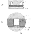
上記のように、弾性シート12に突出部12aを形成した後に成形して得られる樹脂パッケージを用いた発光装置20を図4(a)(b)に示す。樹脂成形体の底面部23bには、裏面のほぼ中央部が最も凹んだ凹部23cが設けられている。この凹部23cの高さ(金属板11の底面からの高さ)や形状は弾性シートの突出部12aの高さや形状によって決められる。このように、樹脂成形体の底面部23bの裏面に凹部23cを設けることで、金属板の貫通孔の幅、すなわち正電極と負電極との間の幅が狭い場合であっても、回路基板へ実装する際の半田の広がりによる短絡を抑制し易くすることができる。更に、樹脂成形体の底面部23bの最下部が、金属板11の裏面よりも高い位置になるようにする、すなわち、実装時に回路基板から浮くようにすることで、半田の溶融時等にかかる成形樹脂への熱的負荷を低減することができる。
4A and 4B show a
図5(a)(b)は、弾性シートを図3(a)(b)とは異なる変形をさせて成形した樹脂パッケージを用いた発光装置30の断面図とその部分拡大図を示す。ここでは、樹脂成形体の底面部33bの裏面が、金属板11に近い側に最も凹んだ凹部33cが形成されている。このような位置に凹部33cを設けることで、金属板11の側面の露出量を多くすることができ、半田のフィレットが形成されやすくなる。また、樹脂成形体の底面部33bの最下面を、金属板11の裏面から高さHの位置となるよう形成することで、半田の溶融時等にかかる熱的負荷を低減することができる。このような形状は、図3(b)のように弾性シートの一部が貫通孔内に突出するように押圧しておき、成形樹脂注入時の圧力を大きくして、弾性シートの突出部を下方向へ押し戻すようにすることで形成することができる。貫通孔の中央付近にかかる押圧力が最も大きくなるため、弾性シートを下部方向から押すと中央部が最も上側に突出し、その突出部を上側から押すと、やはり中央部にかかる押圧力が大きくなるため、下方向に最も押されるのが中央部となり、このような形状となる。図5(c)は、弾性シートの突出部を図5(b)よりも更に強い圧力で押し戻したもので、底面部33bの裏面と金属板11の裏面とが略同一面となるようにしている。このような場合も、底面部33bの中央部により大きな圧力が加わる。このとき、押圧力を制御することで、金属板11と接している底面部33bの端部には微小な凹部33cが形成される。このような小さい凹部にも半田のフィレットを形成することができる。
FIGS. 5A and 5B are a cross-sectional view and a partially enlarged view of a
(弾性シート)
弾性シート12は、金型1、2と金属板12との間にできた隙間に樹脂が入り込みにくくするためのものであり、上下金型の押圧力等によって比較的容易に変形可能な弾性を有するものである。これにより、微細な凹凸や歪みのある金型や金属板の表面形状に応じて変形し、その隙間を減らすことができる。具体的には、ポリイミド、ポリエステル等の耐熱性樹脂を用いることができる。耐熱温度は成形温度や発光素子の実装工程の温度から、120℃〜250℃が好ましい。また、金属板に貼り付け可能な粘着層を有していてもよい。粘着層としては成形時に樹脂バリの発生防止の点から金属板(リードフレーム)と接着性に優れ、また剥がした後に接着剤糊残りが発生すると半田実装不良になることから、剥離性に優れたアクリル系、シリコーン系の材料を粘着材として用いることができる。
(Elastic sheet)
The
弾性シートの厚さは15ミクロン〜100ミクロンの厚さのシートを使用することができる。コスト、生産性の点からより好ましくは20〜60ミクロン、更に好ましくは25ミクロン〜50ミクロンのシートを使用するのが良い。シートの基材、及び粘着層を金属板の貫通孔断面部に貼り付けることで、成形樹脂が貫通孔内に入り込まない為、半田実装時に微細なフィレットとなり半田実装性が向上するなど、発光装置としたときの電気的接合信頼性が向上する。 A sheet having a thickness of 15 to 100 microns can be used as the elastic sheet. From the viewpoint of cost and productivity, it is preferable to use a sheet of 20 to 60 microns, more preferably 25 to 50 microns. By sticking the sheet base material and adhesive layer to the through hole cross section of the metal plate, the molded resin does not enter the through hole, so that it becomes a fine fillet at the time of solder mounting, improving the solder mountability, etc. The electrical connection reliability is improved.
(熱硬化性樹脂)
樹脂パッケージに用いられる熱硬化性樹脂としては、具体的にはエポキシ樹脂組成物、シリコーン樹脂組成物、シリコーン変性エポキシ樹脂などの変性エポキシ樹脂組成物、エポキシ変性シリコーン樹脂などの変性シリコーン樹脂組成物、ポリイミド樹脂組成物、変性ポリイミド樹脂組成物などをあげることができる。特そして、これら樹脂中に充填材(フィラー)としてTiO2、SiO2、Al2O3、MgO、MgCO3、CaCO3、Mg(OH)2、Ca(OH)2などの微粒子などを混入させることで光の透過率を調整し、発光素子からの光の約60%以上を遮光するよう、より好ましくは約90%を遮光するようにするのが好ましい。尚、ここでは基体によって光を反射するか、又は吸収するかどちらでもよいが、発光装置を照明などの用途に用いる場合は、より好ましくは反射させることによって遮光するのが好ましい。そのため、発光素子からの光に対する反射率が60%以上であるものが好ましく、より好ましくは90%以上反射するものが好ましい。例えば、TiO2を用いる場合は、好ましくは10〜30wt%、より好ましくは15〜25wt%配合させるのがよい。これら各種充填材は、1種類のみ、或いは2種類以上を組み合わせて用いることができ、例えば、反射率を調整するための充填材と、膨張係数を調整するための充填材とを併用するなどの用い方ができる。
(Thermosetting resin)
As the thermosetting resin used for the resin package, specifically, an epoxy resin composition, a silicone resin composition, a modified epoxy resin composition such as a silicone-modified epoxy resin, a modified silicone resin composition such as an epoxy-modified silicone resin, Examples thereof include a polyimide resin composition and a modified polyimide resin composition. In particular, fine particles such as TiO 2 , SiO 2 , Al 2 O 3 , MgO, MgCO 3 , CaCO 3 , Mg (OH) 2 , and Ca (OH) 2 are mixed in these resins as fillers. Thus, it is preferable to adjust the light transmittance so that about 60% or more of light from the light emitting element is shielded, more preferably about 90%. Here, either the light may be reflected or absorbed by the substrate, but when the light-emitting device is used for illumination or the like, it is more preferable to shield the light by reflecting it. Therefore, it is preferable that the reflectance with respect to the light from the light emitting element is 60% or more, more preferably 90% or more. For example, when TiO 2 is used, it is preferably added in an amount of 10 to 30 wt%, more preferably 15 to 25 wt%. These various fillers can be used alone or in combination of two or more. For example, a filler for adjusting the reflectance and a filler for adjusting the expansion coefficient are used in combination. Can be used.
また、ディスプレイなどに用いる場合であって、コントラストを向上させたい場合は、発光素子からの光の吸収率が60%以上、より好ましくは90%以上吸収するものが好ましい。このような場合、充填材としては、アセチレンブラック、活性炭、黒鉛などのカーボンや、酸化鉄、二酸化マンガン、酸化コバルト、酸化モリブデンなどの遷移金属酸化物、もしくは有色有機顔料などを目的に応じて利用することができる。 In the case of use in a display or the like, in order to improve the contrast, it is preferable that the light absorption rate from the light emitting element is 60% or more, more preferably 90% or more. In such cases, as the filler, carbon such as acetylene black, activated carbon, graphite, transition metal oxides such as iron oxide, manganese dioxide, cobalt oxide, molybdenum oxide, or colored organic pigments are used depending on the purpose. can do.
また、熱硬化性樹脂の線膨張係数は、5〜35×10−6/Kに調整することが好ましく、さらに好ましくは7〜20×10−6/Kに調整することが望ましい。これにより、基体成型後、冷却時に生じる反りを抑制し易くすることができ、歩留まりよく製造することができる。尚、本明細書において基体の線膨張係数とは、各種充填剤等で調整された熱硬化性樹脂組成物のガラス転移温度以下での線膨張係数を指す。 The linear expansion coefficient of the thermosetting resin is preferably adjusted to 5 to 35 × 10 −6 / K, more preferably 7 to 20 × 10 −6 / K. Thereby, it is possible to easily suppress the warpage that occurs during cooling after the base is molded, and it is possible to manufacture with high yield. In addition, in this specification, the linear expansion coefficient of a base | substrate refers to the linear expansion coefficient below the glass transition temperature of the thermosetting resin composition adjusted with various fillers.
また、別の観点から、熱硬化性樹脂の線膨張係数は、金属板の線膨張係数との差が小さくなるように制御するのが好ましい。好ましくは金属板に対して0.5倍〜2.0倍、より好ましくは0.6倍〜1.4倍とするのがよい。これにより、個片化後の発光装置において、第1及び第2の導電部材と基体とが剥離するのを抑制し、信頼性に優れた光半導体装置とすることができる。 From another point of view, it is preferable to control the linear expansion coefficient of the thermosetting resin so that the difference from the linear expansion coefficient of the metal plate is small. Preferably, it is 0.5 to 2.0 times, more preferably 0.6 to 1.4 times the metal plate. Thereby, in the light emitting device after separation, the first and second conductive members and the base are prevented from peeling off, and an optical semiconductor device having excellent reliability can be obtained.
(金属板)
金属板は、発光素子が載置可能な領域を有する板状部材であり、樹脂成型後に正負一対の電極として機能するような貫通孔を有する。図2に示すような、上下とも平らな面であるものや、一部に凹部や切り欠きが設けられたものも用いることができる。更には、貫通孔の側面に、図6(c)に示すような薄厚部41aを設けてもよい。図6は、ディスプレイに適した黒色系の樹脂を用いた発光装置40を示す図であり、図6(a)は斜視図、図6(b)は底面図、図6(c)はX−X線における断面図である。ディスプレイは、高精細な画像を得るためには発光装置を高密度で配置させるのが好ましいため、図6(b)に示すように金属板41は、樹脂成形体の端部(外側面)から離間するように設けるのが好ましい。そのため、弾性シートの凸部によって形成される底面部43bの凹部43cは、金属板11の裏面の全周囲に形成される。このようにすることで、発光装置の外壁に半田フィレットを形成しなくても密着性よく、しかも高密度で実装することができる。
(Metal plate)
The metal plate is a plate-like member having a region where the light emitting element can be placed, and has a through hole that functions as a pair of positive and negative electrodes after resin molding. As shown in FIG. 2, it is also possible to use a flat surface on both the upper and lower sides or a part provided with a recess or notch. Furthermore, you may provide the
金属板としては、具体的な材料としては、銅、アルミニウム、金、銀、タングステン、鉄、ニッケル、コバルト等の金属又は鉄−ニッケル合金、りん青銅、鉄入り銅、モリブデン、これらは単体又は合金として用いることができる。更に、最表面に、発光素子からの光を反射可能な材料を設けるのが好ましく、具体的には金、銀、銅、Pt、Pd、Al、W、Mo、Ru、Rh等が好ましい。特に、可視域の反射率は70%以上である事が好ましく、Ag、Ru、Rh、Pt、Pdなどが好的に用いられる。また、金属板の表面光沢が高いほうがよく好ましくは0.5以上、より好ましくは1.0以上である。ここで示される光沢度は日本電色製 微小面色差計VSR 300Aを用い、45°照射、垂直受光で得られる数字である。 Specific materials for the metal plate include copper, aluminum, gold, silver, tungsten, iron, nickel, cobalt, and other metals or iron-nickel alloys, phosphor bronze, iron-containing copper, molybdenum, and these are simple or alloys. Can be used as Furthermore, a material capable of reflecting light from the light emitting element is preferably provided on the outermost surface, and specifically, gold, silver, copper, Pt, Pd, Al, W, Mo, Ru, Rh, and the like are preferable. In particular, the reflectance in the visible range is preferably 70% or more, and Ag, Ru, Rh, Pt, Pd, etc. are preferably used. Further, the surface gloss of the metal plate is preferably higher, preferably 0.5 or more, more preferably 1.0 or more. The glossiness shown here is a number obtained by 45 ° irradiation and vertical light reception using a Nippon Denshoku micro surface color difference meter VSR 300A.
<実施の形態2>
図7(a)(b)(c)(d)は、第1金型(上金型)1側にも弾性シート72を設けた樹脂パッケージの製造方法を説明する図である。ここでは、図7(a)に示すように、第1金型(上金型1)に弾性シート72を貼り付けている。このように金属板11の上下ともに弾性シートを設けて金型で挟持することで、金属板にかかる押圧力をその弾性シートで吸収することができる。そのため、金属板11の変形を低減することができ、貫通孔11aの幅の変動を少なくすることができる。更に、発光素子を実装する側の面、すなわち金属板11の上面にも、成型時に樹脂が入り込むことを抑制することができるため、実装不良や導電性ワイヤの接続不良を抑制することができる。さらに、金型と金属板とを直接触れないようにすることができるため、金属板の上面を損傷しにくくして、メッキなどにより高光沢加工を施した面を、そのままの状態で保つことができる。上金型側に設ける弾性シートは、下金型側に設ける弾性シートと同種のものを用いることができる。
<
7A, 7B, 7C, and 7D are views for explaining a method of manufacturing a resin package in which an
本発明に係る樹脂パッケージの製造方法は、成型時にバリの発生を抑制し、耐熱性に優れた樹脂パッケージを歩留まりよく得ることができるため、各種発光装置等に用いられる樹脂パッケージとして用いることができる。 The method for producing a resin package according to the present invention can be used as a resin package used in various light emitting devices and the like because it can suppress the generation of burrs during molding and can obtain a resin package having excellent heat resistance with a high yield. .
1…第1金型(上金型)
1a…樹脂注入口
1b…凹部
2…第2金型(下金型)
10、20、30、40…発光装置
11、41…金属板(リードフレーム)
11a…貫通孔
41a…薄厚部
12、72…弾性シート
12a…弾性シートの突出部
13、43…樹脂成形体(パッケージ)
13a、43a…側壁部
13b、23b、33b、43b…底面部
23c、33c、43c…裏面凹部
14…発光素子
15…導電性ワイヤ
16…封止部材
103…リフレクター
104…Ni/Agめっき
105…金属配線
200…光半導体素子搭載領域(凹部)
300…樹脂注入口
301…金型
1 ... 1st mold (upper mold)
DESCRIPTION OF
10, 20, 30, 40 ...
11a ... Through
13a, 43a ...
300 ...
Claims (5)
前記金属板は貫通孔を有し、
該貫通孔内に設けられる前記樹脂成形体の底面部の裏面において、その中央部が最も下方向に突出しており、
前記底面部の裏面と、前記貫通孔の側面の一部とによって、底面に凹部を有することを特徴とする樹脂パッケージ。 A resin package comprising a resin molded body and a metal plate,
The metal plate has a through hole;
In the back surface of the bottom surface portion of the resin molded body provided in the through hole, the center portion protrudes most downward,
A resin package having a recess on a bottom surface by a back surface of the bottom surface portion and a part of a side surface of the through hole .
Priority Applications (1)
| Application Number | Priority Date | Filing Date | Title |
|---|---|---|---|
| JP2010230445A JP5771937B2 (en) | 2010-10-13 | 2010-10-13 | Resin package and manufacturing method thereof, and light emitting device using resin package |
Applications Claiming Priority (1)
| Application Number | Priority Date | Filing Date | Title |
|---|---|---|---|
| JP2010230445A JP5771937B2 (en) | 2010-10-13 | 2010-10-13 | Resin package and manufacturing method thereof, and light emitting device using resin package |
Publications (3)
| Publication Number | Publication Date |
|---|---|
| JP2012084724A JP2012084724A (en) | 2012-04-26 |
| JP2012084724A5 JP2012084724A5 (en) | 2013-11-28 |
| JP5771937B2 true JP5771937B2 (en) | 2015-09-02 |
Family
ID=46243294
Family Applications (1)
| Application Number | Title | Priority Date | Filing Date |
|---|---|---|---|
| JP2010230445A Active JP5771937B2 (en) | 2010-10-13 | 2010-10-13 | Resin package and manufacturing method thereof, and light emitting device using resin package |
Country Status (1)
| Country | Link |
|---|---|
| JP (1) | JP5771937B2 (en) |
Families Citing this family (7)
| Publication number | Priority date | Publication date | Assignee | Title |
|---|---|---|---|---|
| JP2013251422A (en) * | 2012-06-01 | 2013-12-12 | Apic Yamada Corp | Substrate for mounting led chip, led package, mold, and manufacturing methods of substrate for mounting led chip and led package |
| JP6147976B2 (en) * | 2012-09-26 | 2017-06-14 | ローム株式会社 | LIGHT EMITTING DEVICE AND LIGHT EMITTING UNIT MANUFACTURING METHOD |
| JP6484396B2 (en) * | 2013-06-28 | 2019-03-13 | 日亜化学工業株式会社 | Light emitting device package and light emitting device using the same |
| JP2015126091A (en) * | 2013-12-26 | 2015-07-06 | 大日本印刷株式会社 | Manufacturing method of lead frame with resin, manufacturing method of semiconductor device, injection molding die device, and lead frame with resin |
| JP6398563B2 (en) | 2014-05-29 | 2018-10-03 | 日亜化学工業株式会社 | Light emitting device |
| DE102014116370A1 (en) * | 2014-11-10 | 2016-05-12 | Osram Opto Semiconductors Gmbh | Method for producing a carrier and method for producing an optoelectronic component |
| JP6443429B2 (en) * | 2016-11-30 | 2018-12-26 | 日亜化学工業株式会社 | Package, package manufacturing method, light emitting device, and light emitting device manufacturing method |
Family Cites Families (2)
| Publication number | Priority date | Publication date | Assignee | Title |
|---|---|---|---|---|
| JP2003001674A (en) * | 2001-06-26 | 2003-01-08 | Nec Kansai Ltd | Resin molding apparatus |
| JP2008244143A (en) * | 2007-03-27 | 2008-10-09 | Toshiba Corp | Method of manufacturing semiconductor light-emitting device |
-
2010
- 2010-10-13 JP JP2010230445A patent/JP5771937B2/en active Active
Also Published As
| Publication number | Publication date |
|---|---|
| JP2012084724A (en) | 2012-04-26 |
Similar Documents
| Publication | Publication Date | Title |
|---|---|---|
| JP5771937B2 (en) | Resin package and manufacturing method thereof, and light emitting device using resin package | |
| JP5038623B2 (en) | Optical semiconductor device and manufacturing method thereof | |
| US9379290B2 (en) | LED module | |
| JP4910220B1 (en) | LED module device and manufacturing method thereof | |
| US8080436B2 (en) | Light emitting device and method of manufacturing the light emitting device | |
| US20090166664A1 (en) | High power light emitting diode package and manufacturing method thereof | |
| JP4914998B1 (en) | LED module device and manufacturing method thereof | |
| JP5423475B2 (en) | Manufacturing method of optical semiconductor device | |
| JP5860289B2 (en) | Manufacturing method of LED device | |
| WO2008047933A1 (en) | Package assembly for upper/lower electrode light-emitting diodes and light-emitting device manufacturing method using same | |
| JP2010003743A (en) | Light-emitting device | |
| JP5940799B2 (en) | Electronic component mounting package, electronic component package, and manufacturing method thereof | |
| JP2016072524A (en) | Light emitting device and manufacturing method of the same | |
| JP2014187081A (en) | Light-emitting device | |
| JP2009188187A (en) | Electronic part and manufacturing method thereof | |
| JP4904604B1 (en) | LED module device and manufacturing method thereof | |
| KR20090072941A (en) | High Power LED Package and Fabricating Method thereof | |
| JP6021416B2 (en) | Lead frame with reflector for optical semiconductor device, optical semiconductor device using the same, and manufacturing method thereof | |
| JP2012182357A (en) | Lead frame substrate for led light emitting element, led light emitting element device, and lead frame for the led light emitting element | |
| JP5493549B2 (en) | Light emitting device and manufacturing method thereof | |
| WO2011055786A1 (en) | Light-emitting device | |
| JP2006100753A (en) | Semiconductor module and its manufacturing method | |
| JP5359662B2 (en) | Light emitting device and manufacturing method thereof | |
| US20190312188A1 (en) | Base member, and method of manufacturing light emitting device using same | |
| JP5381684B2 (en) | Method for manufacturing light emitting device |
Legal Events
| Date | Code | Title | Description |
|---|---|---|---|
| A621 | Written request for application examination |
Free format text: JAPANESE INTERMEDIATE CODE: A621 Effective date: 20130904 |
|
| A521 | Request for written amendment filed |
Free format text: JAPANESE INTERMEDIATE CODE: A523 Effective date: 20131010 |
|
| A977 | Report on retrieval |
Free format text: JAPANESE INTERMEDIATE CODE: A971007 Effective date: 20140423 |
|
| A131 | Notification of reasons for refusal |
Free format text: JAPANESE INTERMEDIATE CODE: A131 Effective date: 20140507 |
|
| A521 | Request for written amendment filed |
Free format text: JAPANESE INTERMEDIATE CODE: A523 Effective date: 20140704 |
|
| A131 | Notification of reasons for refusal |
Free format text: JAPANESE INTERMEDIATE CODE: A131 Effective date: 20150120 |
|
| A521 | Request for written amendment filed |
Free format text: JAPANESE INTERMEDIATE CODE: A523 Effective date: 20150312 |
|
| TRDD | Decision of grant or rejection written | ||
| A01 | Written decision to grant a patent or to grant a registration (utility model) |
Free format text: JAPANESE INTERMEDIATE CODE: A01 Effective date: 20150602 |
|
| A61 | First payment of annual fees (during grant procedure) |
Free format text: JAPANESE INTERMEDIATE CODE: A61 Effective date: 20150615 |
|
| R150 | Certificate of patent or registration of utility model |
Ref document number: 5771937 Country of ref document: JP Free format text: JAPANESE INTERMEDIATE CODE: R150 |
|
| R250 | Receipt of annual fees |
Free format text: JAPANESE INTERMEDIATE CODE: R250 |
|
| R250 | Receipt of annual fees |
Free format text: JAPANESE INTERMEDIATE CODE: R250 |
|
| R250 | Receipt of annual fees |
Free format text: JAPANESE INTERMEDIATE CODE: R250 |
|
| R250 | Receipt of annual fees |
Free format text: JAPANESE INTERMEDIATE CODE: R250 |
|
| R250 | Receipt of annual fees |
Free format text: JAPANESE INTERMEDIATE CODE: R250 |
|
| R250 | Receipt of annual fees |
Free format text: JAPANESE INTERMEDIATE CODE: R250 |