JP5743066B2 - 光検出回路、光検出方法、表示パネルおよび表示装置 - Google Patents
光検出回路、光検出方法、表示パネルおよび表示装置 Download PDFInfo
- Publication number
- JP5743066B2 JP5743066B2 JP2011048320A JP2011048320A JP5743066B2 JP 5743066 B2 JP5743066 B2 JP 5743066B2 JP 2011048320 A JP2011048320 A JP 2011048320A JP 2011048320 A JP2011048320 A JP 2011048320A JP 5743066 B2 JP5743066 B2 JP 5743066B2
- Authority
- JP
- Japan
- Prior art keywords
- voltage
- transistor
- circuit
- line
- light detection
- Prior art date
- Legal status (The legal status is an assumption and is not a legal conclusion. Google has not performed a legal analysis and makes no representation as to the accuracy of the status listed.)
- Active
Links
- 238000000034 method Methods 0.000 title claims description 11
- 238000001514 detection method Methods 0.000 claims description 140
- 238000010586 diagram Methods 0.000 description 29
- 230000008859 change Effects 0.000 description 26
- 241000750042 Vini Species 0.000 description 19
- 230000004048 modification Effects 0.000 description 13
- 238000012986 modification Methods 0.000 description 13
- 239000003990 capacitor Substances 0.000 description 12
- 230000004044 response Effects 0.000 description 8
- 230000007423 decrease Effects 0.000 description 6
- 239000010410 layer Substances 0.000 description 6
- 230000003071 parasitic effect Effects 0.000 description 6
- 230000006866 deterioration Effects 0.000 description 4
- 230000003287 optical effect Effects 0.000 description 4
- 230000006872 improvement Effects 0.000 description 3
- 230000000052 comparative effect Effects 0.000 description 2
- 230000007547 defect Effects 0.000 description 2
- 230000000694 effects Effects 0.000 description 2
- 230000005525 hole transport Effects 0.000 description 2
- 238000002347 injection Methods 0.000 description 2
- 239000007924 injection Substances 0.000 description 2
- 230000001678 irradiating effect Effects 0.000 description 2
- 230000002427 irreversible effect Effects 0.000 description 2
- 239000004973 liquid crystal related substance Substances 0.000 description 2
- 239000011159 matrix material Substances 0.000 description 2
- 239000012044 organic layer Substances 0.000 description 2
- 230000015556 catabolic process Effects 0.000 description 1
- 230000009194 climbing Effects 0.000 description 1
- 238000006731 degradation reaction Methods 0.000 description 1
- 238000005401 electroluminescence Methods 0.000 description 1
- 230000003760 hair shine Effects 0.000 description 1
- 230000010365 information processing Effects 0.000 description 1
- 230000014759 maintenance of location Effects 0.000 description 1
- 230000006798 recombination Effects 0.000 description 1
- 238000005215 recombination Methods 0.000 description 1
- 239000010409 thin film Substances 0.000 description 1
Images


Classifications
-
- G—PHYSICS
- G01—MEASURING; TESTING
- G01J—MEASUREMENT OF INTENSITY, VELOCITY, SPECTRAL CONTENT, POLARISATION, PHASE OR PULSE CHARACTERISTICS OF INFRARED, VISIBLE OR ULTRAVIOLET LIGHT; COLORIMETRY; RADIATION PYROMETRY
- G01J1/00—Photometry, e.g. photographic exposure meter
- G01J1/42—Photometry, e.g. photographic exposure meter using electric radiation detectors
- G01J1/44—Electric circuits
- G01J1/46—Electric circuits using a capacitor
-
- G—PHYSICS
- G09—EDUCATION; CRYPTOGRAPHY; DISPLAY; ADVERTISING; SEALS
- G09G—ARRANGEMENTS OR CIRCUITS FOR CONTROL OF INDICATING DEVICES USING STATIC MEANS TO PRESENT VARIABLE INFORMATION
- G09G3/00—Control arrangements or circuits, of interest only in connection with visual indicators other than cathode-ray tubes
- G09G3/20—Control arrangements or circuits, of interest only in connection with visual indicators other than cathode-ray tubes for presentation of an assembly of a number of characters, e.g. a page, by composing the assembly by combination of individual elements arranged in a matrix no fixed position being assigned to or needed to be assigned to the individual characters or partial characters
- G09G3/22—Control arrangements or circuits, of interest only in connection with visual indicators other than cathode-ray tubes for presentation of an assembly of a number of characters, e.g. a page, by composing the assembly by combination of individual elements arranged in a matrix no fixed position being assigned to or needed to be assigned to the individual characters or partial characters using controlled light sources
- G09G3/30—Control arrangements or circuits, of interest only in connection with visual indicators other than cathode-ray tubes for presentation of an assembly of a number of characters, e.g. a page, by composing the assembly by combination of individual elements arranged in a matrix no fixed position being assigned to or needed to be assigned to the individual characters or partial characters using controlled light sources using electroluminescent panels
- G09G3/32—Control arrangements or circuits, of interest only in connection with visual indicators other than cathode-ray tubes for presentation of an assembly of a number of characters, e.g. a page, by composing the assembly by combination of individual elements arranged in a matrix no fixed position being assigned to or needed to be assigned to the individual characters or partial characters using controlled light sources using electroluminescent panels semiconductive, e.g. using light-emitting diodes [LED]
- G09G3/3208—Control arrangements or circuits, of interest only in connection with visual indicators other than cathode-ray tubes for presentation of an assembly of a number of characters, e.g. a page, by composing the assembly by combination of individual elements arranged in a matrix no fixed position being assigned to or needed to be assigned to the individual characters or partial characters using controlled light sources using electroluminescent panels semiconductive, e.g. using light-emitting diodes [LED] organic, e.g. using organic light-emitting diodes [OLED]
- G09G3/3225—Control arrangements or circuits, of interest only in connection with visual indicators other than cathode-ray tubes for presentation of an assembly of a number of characters, e.g. a page, by composing the assembly by combination of individual elements arranged in a matrix no fixed position being assigned to or needed to be assigned to the individual characters or partial characters using controlled light sources using electroluminescent panels semiconductive, e.g. using light-emitting diodes [LED] organic, e.g. using organic light-emitting diodes [OLED] using an active matrix
- G09G3/3233—Control arrangements or circuits, of interest only in connection with visual indicators other than cathode-ray tubes for presentation of an assembly of a number of characters, e.g. a page, by composing the assembly by combination of individual elements arranged in a matrix no fixed position being assigned to or needed to be assigned to the individual characters or partial characters using controlled light sources using electroluminescent panels semiconductive, e.g. using light-emitting diodes [LED] organic, e.g. using organic light-emitting diodes [OLED] using an active matrix with pixel circuitry controlling the current through the light-emitting element
-
- G—PHYSICS
- G09—EDUCATION; CRYPTOGRAPHY; DISPLAY; ADVERTISING; SEALS
- G09G—ARRANGEMENTS OR CIRCUITS FOR CONTROL OF INDICATING DEVICES USING STATIC MEANS TO PRESENT VARIABLE INFORMATION
- G09G2320/00—Control of display operating conditions
- G09G2320/04—Maintaining the quality of display appearance
- G09G2320/043—Preventing or counteracting the effects of ageing
-
- G—PHYSICS
- G09—EDUCATION; CRYPTOGRAPHY; DISPLAY; ADVERTISING; SEALS
- G09G—ARRANGEMENTS OR CIRCUITS FOR CONTROL OF INDICATING DEVICES USING STATIC MEANS TO PRESENT VARIABLE INFORMATION
- G09G2360/00—Aspects of the architecture of display systems
- G09G2360/14—Detecting light within display terminals, e.g. using a single or a plurality of photosensors
- G09G2360/145—Detecting light within display terminals, e.g. using a single or a plurality of photosensors the light originating from the display screen
Description
(A)制御線の電圧を、フォトダイオードに順バイアスを印加するとともにトランジスタをオフ状態とする第1電圧に設定するとともに、光検出線の電圧を初期化する第1ステップ
(B)制御線の電圧を、フォトダイオードに逆バイアスを印加するとともにトランジスタをオフ状態とする第2電圧(前記第2電圧>前記第1電圧)に設定する第2ステップ
(C)制御線の電圧を、フォトダイオードに逆バイアスを印加するとともにトランジスタをオン状態とする第3電圧(前記第3電圧>前記第2電圧)に設定する第3ステップ
1.実施の形態(表示装置)
光検出回路においてトランジスタのドレインとフォトダイオードの
アノードとが互いに異なる配線に接続されている例
2.変形例(表示装置)
光検出回路においてトランジスタのドレインとフォトダイオードの
アノードとが共通の配線に接続されている例
3.参考例(入力装置)
[構成]
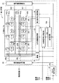
図1は、本発明の一実施の形態に係る表示装置1の全体構成の一例を表したものである。この表示装置1は、表示パネル10と、表示パネル10の周辺に形成された駆動回路20とを備えている。
表示パネル10は、複数の画素11を表示パネル10の全面に渡って2次元配置したものである。表示パネル10は、各画素11をアクティブマトリクス駆動することにより、外部から入力された映像信号20Aに基づく画像を表示するものである。各画素11は、例えば、赤色用の画素11Rと、緑色用の画素11Gと、青色用の画素11Bとを含んでいる。
駆動回路20は、例えば、図1に示したように、タイミング制御回路21、映像信号処理回路22、信号線駆動回路23、書込線駆動回路24および制御線駆動回路25を有している。さらに、駆動回路20は、例えば、図1に示したように、受光信号処理回路26、記憶回路27および電源28を有している。
次に、本実施の形態の光検出回路14の効果について、比較例と対比して説明する。
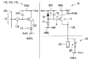
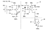
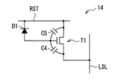
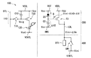
図13は、上記実施の形態に係る光検出回路14の一変形例を表したものである。本変形例に係る光検出回路14では、トランジスタT1に対して電源線VDDLの代わりに、制御線RSTが接続されている。本変形例に係る光検出回路14を含む表示装置1の基本的な動作は、上記実施の形態に係る光検出回路14を含む表示装置1の動作と同じである。つまり、制御線RSTをVssとすることでトランジスタT1のゲート電位を初期化し、次にViniとすることでトランジスタT1をオフした状態でフォトダイオードD1に電位差を発生させ光検出が行われる。最後に、制御線RSTの電位をVdd2とすることでトランジスタT1をオン状態とし、検出信号を光検出線LDLに出力させる。ただし、本変形例では、トランジスタT1のゲート電圧の変動が光検出線LDLに入力されてしまうので、例えば、図14に示したように、出力期間t4の直前に光検出線LDLの電位をViniに初期化する必要がある。
図18は、参考例に係る入力装置2の全体構成の一例を表したものである。この入力装置2は、入力パネル30と、入力パネル30の周辺に形成された駆動回路40とを備えている。
入力パネル30は、複数の光検出回路14を入力パネル30の全面に渡って2次元配置したものである。入力パネル30は、各光検出回路14をライン駆動することにより、外部から入力された映像信号20Aに基づく画像を表示するものである。光検出回路14は、例えば、図3、図13、図15、図16または図17に示した構成となっている。
駆動回路40は、例えば、図18に示したように、タイミング制御回路21、制御線駆動回路25、受光信号処理回路26および電源28を有している。
Claims (5)
- 表示パネルと、
前記表示パネルを駆動する駆動回路と
を備え、
前記表示パネルは、
自発光素子を含む複数の画素と、
前記画素から発せられた光を検出する複数の光検出回路と
を有し、
前記光検出回路は、
固定電源線と光検出線との間に設けられたトランジスタと、
前記トランジスタのゲートと制御線との間に設けられるとともに、カソードが前記制御線側を向くように配置されたフォトダイオードと
を有し、
前記駆動回路は、前記フォトダイオードに順バイアスを印加するとともに前記トランジスタをオフ状態とする第1電圧と、前記フォトダイオードに逆バイアスを印加するとともに前記トランジスタをオフ状態とする第2電圧(前記第2電圧>前記第1電圧)と、前記フォトダイオードに逆バイアスを印加するとともに前記トランジスタをオン状態とする第3電圧(前記第3電圧>前記第2電圧)とを順次、前記制御線に出力する電源を有する
表示装置。 - 前記駆動回路は、前記光検出線に接続された受光信号処理回路をさらに有し、
前記受光信号処理回路は、
前記光検出線の電圧を検出する電圧検出部と、
前記光検出線の電圧を第4電圧(前記第4電圧>前記第1電圧)で初期化する初期化部と
を有する
請求項1に記載の表示装置。 - 前記駆動回路は、前記電圧検出部で検出された電圧の大きさに応じて映像信号を補正する信号処理回路をさらに有する
請求項2に記載の表示装置。 - 固定電源線と光検出線との間に設けられたトランジスタと、前記トランジスタのゲートと制御線との間に設けられると共にカソードが前記制御線側を向くように配置されたフォトダイオードとを備えた光検出回路を用いて、入射光を検出する光検出方法であって、
前記制御線の電圧を、前記フォトダイオードに順バイアスを印加するとともに前記トランジスタをオフ状態とする第1電圧に設定するとともに、前記光検出線の電圧を初期化する第1ステップと、
前記制御線の電圧を、前記フォトダイオードに逆バイアスを印加するとともに前記トランジスタをオフ状態とする第2電圧(前記第2電圧>前記第1電圧)に設定する第2ステップと、
前記制御線の電圧を、前記フォトダイオードに逆バイアスを印加するとともに前記トランジスタをオン状態とする第3電圧(前記第3電圧>前記第2電圧)に設定する第3ステップと
を含む
光検出方法。 - 前記第2ステップと前記第3ステップとの間に、前記光検出線の電圧を再度、初期化する第4ステップを含む
請求項4に記載の光検出方法。
Priority Applications (2)
| Application Number | Priority Date | Filing Date | Title |
|---|---|---|---|
| JP2011048320A JP5743066B2 (ja) | 2011-03-04 | 2011-03-04 | 光検出回路、光検出方法、表示パネルおよび表示装置 |
| US13/406,060 US20120223925A1 (en) | 2011-03-04 | 2012-02-27 | Photodetection circuit, photodetection method, display panel, and display |
Applications Claiming Priority (1)
| Application Number | Priority Date | Filing Date | Title |
|---|---|---|---|
| JP2011048320A JP5743066B2 (ja) | 2011-03-04 | 2011-03-04 | 光検出回路、光検出方法、表示パネルおよび表示装置 |
Publications (3)
| Publication Number | Publication Date |
|---|---|
| JP2012186313A JP2012186313A (ja) | 2012-09-27 |
| JP2012186313A5 JP2012186313A5 (ja) | 2014-04-03 |
| JP5743066B2 true JP5743066B2 (ja) | 2015-07-01 |
Family
ID=46753008
Family Applications (1)
| Application Number | Title | Priority Date | Filing Date |
|---|---|---|---|
| JP2011048320A Active JP5743066B2 (ja) | 2011-03-04 | 2011-03-04 | 光検出回路、光検出方法、表示パネルおよび表示装置 |
Country Status (2)
| Country | Link |
|---|---|
| US (1) | US20120223925A1 (ja) |
| JP (1) | JP5743066B2 (ja) |
Families Citing this family (3)
| Publication number | Priority date | Publication date | Assignee | Title |
|---|---|---|---|---|
| WO2018087787A1 (en) * | 2016-11-14 | 2018-05-17 | Alma Mater Studiorum - Universita' Di Bologna | Sensitive field effect device and manufacturing method thereof |
| US11715322B2 (en) * | 2020-11-20 | 2023-08-01 | Novatek Microelectronics Corp. | Fingerprint sensing apparatus, fingerprint readout circuit, and touch display panel |
| US11709565B2 (en) * | 2020-12-23 | 2023-07-25 | Novatek Microelectronics Corp. | Fingerprint sensing apparatus, fingerprint readout circuit, and touch display panel |
Family Cites Families (10)
| Publication number | Priority date | Publication date | Assignee | Title |
|---|---|---|---|---|
| US6246436B1 (en) * | 1997-11-03 | 2001-06-12 | Agilent Technologies, Inc | Adjustable gain active pixel sensor |
| JP2007096387A (ja) * | 2005-09-27 | 2007-04-12 | Seiko Precision Inc | イメージセンサ、画像処理装置及び画像処理プログラム |
| GB2439118A (en) * | 2006-06-12 | 2007-12-19 | Sharp Kk | Image sensor and display |
| JP4959449B2 (ja) * | 2006-12-27 | 2012-06-20 | 三星モバイルディスプレイ株式會社 | 周辺光感知回路及びこれを有する平板表示装置 |
| JP5269456B2 (ja) * | 2008-03-26 | 2013-08-21 | 株式会社東芝 | イメージセンサおよびその駆動方法 |
| US20100321356A1 (en) * | 2008-05-12 | 2010-12-23 | Sharp Kabushiki Kaihsa | Thin-film transistor, photodetector circuit including the same, and display device |
| JP5272885B2 (ja) * | 2009-05-12 | 2013-08-28 | ソニー株式会社 | 表示装置、光検出動作の制御方法 |
| JP2010266492A (ja) * | 2009-05-12 | 2010-11-25 | Sony Corp | 画素回路、表示装置、画素回路の駆動方法 |
| JP2012160772A (ja) * | 2009-06-04 | 2012-08-23 | Sharp Corp | 光センサおよび表示装置 |
| JP2011043729A (ja) * | 2009-08-24 | 2011-03-03 | Sony Corp | 表示装置および電子機器 |
-
2011
- 2011-03-04 JP JP2011048320A patent/JP5743066B2/ja active Active
-
2012
- 2012-02-27 US US13/406,060 patent/US20120223925A1/en not_active Abandoned
Also Published As
| Publication number | Publication date |
|---|---|
| US20120223925A1 (en) | 2012-09-06 |
| JP2012186313A (ja) | 2012-09-27 |
Similar Documents
| Publication | Publication Date | Title |
|---|---|---|
| US10997926B2 (en) | Driving controller, display device and driving method including a lower frequency mode and an image transition mode | |
| US10796637B2 (en) | Display device | |
| KR102603596B1 (ko) | 유기발광 표시장치와 그의 열화 센싱 방법 | |
| JP6606580B2 (ja) | 有機発光表示装置とその劣化センシング方法 | |
| US8842060B2 (en) | Display device | |
| US7605792B2 (en) | Driving method and circuit for automatic voltage output of active matrix organic light emitting device and data drive circuit using the same | |
| US9183780B2 (en) | Organic light emitting display | |
| JP5562327B2 (ja) | 表示装置及びその駆動方法 | |
| JP5449641B2 (ja) | 表示装置 | |
| US8390653B2 (en) | Electroluminescent pixel with efficiency compensation by threshold voltage overcompensation | |
| KR101578761B1 (ko) | 픽셀 트랜지스터 이동도에서의 변화를 보상하는 디스플레이 디바이스 | |
| JP2008203478A (ja) | 表示装置とその駆動方法 | |
| JP2011141418A (ja) | 表示装置、光検出方法、電子機器 | |
| JP2008164796A (ja) | 画素回路および表示装置とその駆動方法 | |
| JP2010266492A (ja) | 画素回路、表示装置、画素回路の駆動方法 | |
| JP5272885B2 (ja) | 表示装置、光検出動作の制御方法 | |
| US9001099B2 (en) | Image display and image display method | |
| JP5743066B2 (ja) | 光検出回路、光検出方法、表示パネルおよび表示装置 | |
| CN110853582A (zh) | 像素及其控制方法、有机发光二极管显示器 | |
| JP2008197607A (ja) | 画素回路、画像表示装置及びその駆動方法 | |
| JP5239773B2 (ja) | 表示装置 | |
| JP5192208B2 (ja) | 画像表示装置 | |
| JP5228823B2 (ja) | 表示装置 | |
| TW201331913A (zh) | 像素電路、具備其之顯示裝置、及像素電路之控制方法 | |
| JP2008242322A (ja) | 発光表示装置 |
Legal Events
| Date | Code | Title | Description |
|---|---|---|---|
| A521 | Request for written amendment filed |
Free format text: JAPANESE INTERMEDIATE CODE: A523 Effective date: 20140214 |
|
| A621 | Written request for application examination |
Free format text: JAPANESE INTERMEDIATE CODE: A621 Effective date: 20140214 |
|
| A131 | Notification of reasons for refusal |
Free format text: JAPANESE INTERMEDIATE CODE: A131 Effective date: 20150106 |
|
| A521 | Request for written amendment filed |
Free format text: JAPANESE INTERMEDIATE CODE: A523 Effective date: 20150220 |
|
| TRDD | Decision of grant or rejection written | ||
| A01 | Written decision to grant a patent or to grant a registration (utility model) |
Free format text: JAPANESE INTERMEDIATE CODE: A01 Effective date: 20150331 |
|
| A711 | Notification of change in applicant |
Free format text: JAPANESE INTERMEDIATE CODE: A712 Effective date: 20150327 |
|
| A61 | First payment of annual fees (during grant procedure) |
Free format text: JAPANESE INTERMEDIATE CODE: A61 Effective date: 20150421 |
|
| R150 | Certificate of patent or registration of utility model |
Ref document number: 5743066 Country of ref document: JP Free format text: JAPANESE INTERMEDIATE CODE: R150 |
|
| R250 | Receipt of annual fees |
Free format text: JAPANESE INTERMEDIATE CODE: R250 |
|
| R250 | Receipt of annual fees |
Free format text: JAPANESE INTERMEDIATE CODE: R250 |
|
| R250 | Receipt of annual fees |
Free format text: JAPANESE INTERMEDIATE CODE: R250 |
|
| R250 | Receipt of annual fees |
Free format text: JAPANESE INTERMEDIATE CODE: R250 |
|
| R250 | Receipt of annual fees |
Free format text: JAPANESE INTERMEDIATE CODE: R250 |
|
| S303 | Written request for registration of pledge or change of pledge |
Free format text: JAPANESE INTERMEDIATE CODE: R316303 |
|
| R350 | Written notification of registration of transfer |
Free format text: JAPANESE INTERMEDIATE CODE: R350 |
|
| R250 | Receipt of annual fees |
Free format text: JAPANESE INTERMEDIATE CODE: R250 |
|
| S803 | Written request for registration of cancellation of provisional registration |
Free format text: JAPANESE INTERMEDIATE CODE: R316803 |
|
| R350 | Written notification of registration of transfer |
Free format text: JAPANESE INTERMEDIATE CODE: R350 |