JP5735680B2 - Semiconductor device and manufacturing method thereof - Google Patents
Semiconductor device and manufacturing method thereof Download PDFInfo
- Publication number
- JP5735680B2 JP5735680B2 JP2014095979A JP2014095979A JP5735680B2 JP 5735680 B2 JP5735680 B2 JP 5735680B2 JP 2014095979 A JP2014095979 A JP 2014095979A JP 2014095979 A JP2014095979 A JP 2014095979A JP 5735680 B2 JP5735680 B2 JP 5735680B2
- Authority
- JP
- Japan
- Prior art keywords
- layer
- etching stopper
- insulating film
- etching
- stopper layer
- Prior art date
- Legal status (The legal status is an assumption and is not a legal conclusion. Google has not performed a legal analysis and makes no representation as to the accuracy of the status listed.)
- Expired - Lifetime
Links
Images


Description
本発明は、半導体装置およびその製造方法に関し、特に、DRAMのキャパシタ上層に形成した金属配線層から半導体基板上に形成された不純物拡散層とゲート電極に接続するコンタクトを接合リークを増大させることなく安定して形成できるデバイス構造とその製造方法に関するものである。 The present invention relates to a semiconductor device and a method for manufacturing the same, and more particularly to a contact connecting an impurity diffusion layer formed on a semiconductor substrate and a gate electrode from a metal wiring layer formed on a capacitor upper layer of a DRAM without increasing junction leakage. The present invention relates to a device structure that can be stably formed and a manufacturing method thereof.
従来のDRAMセルとロジックを混載したLSIデバイスについて図37、図38、図39により説明する。 A conventional LSI device mixed with a DRAM cell and logic will be described with reference to FIGS. 37, 38, and 39. FIG.
図38は、一個のMOSトランジスタを中心にした拡大断面図である。図38に示すように、半導体基板91表面に、DRAMセルの上層に形成した金属配線層(図示せず)から半導体基板91上に形成された不純物拡散層93とゲート電極92に接続するようにコンタクトホール94が設けられている。DRAMメモリセルのキャパシタは、高密度化を達成しようとすると、キャパシタの占有面積を増大させることなく容量を大きく確保する必要があり、高さを高く形成することが要求される。そのため、非常に深いコンタクトが必要になるので、その分だけ長くエッチング工程を行う必要があり、これに伴いコンタクトホール94も過剰にエッチングされてしまいがちである。
FIG. 38 is an enlarged cross-sectional view centering on one MOS transistor. As shown in FIG. 38, the surface of the
図38に図示されるように、コンタクトホール94のアスペクト比(「コンタクトの深さ」/「コンタクトホールの直径」の比)は5から10になり、半導体基板91の不純物拡散層93や素子間分離膜(図示せず)をエッチングにより削ることなく形成することが非常に困難であり、最悪は接合界面を越えて開口が形成され、接合リークの増大を招いてしまう。
As shown in FIG. 38, the aspect ratio of the contact hole 94 (ratio of “contact depth” / “contact hole diameter”) is from 5 to 10, and the
そこで特開平10-79430号公報には、改良技術として、半導体基板上のコンタクト開口部にエッチングストッパ層となるシリコン窒化膜を形成することにより不純物拡散層をエッチングにより削ることなく形成し接合リークの増大を防止する技術が開示されている。 Therefore, in Japanese Patent Laid-Open No. 10-79430, as an improved technique, an impurity diffusion layer is formed without etching by etching by forming a silicon nitride film as an etching stopper layer in a contact opening on a semiconductor substrate. A technique for preventing the increase is disclosed.
一方、図37に示すように、DRAMセルとロジックを混載したLSIデバイスにおいては、不純物拡散層93とそれに接続するコンタクトホール94との位置合わせマージンを大きくとることができず、図37に描かれるように、コンタクトホール94は不純物拡散層93と素子分離絶縁膜95との境界に開口することがある。
On the other hand, as shown in FIG. 37, in an LSI device in which DRAM cells and logic are mixedly mounted, the alignment margin between the
このような場合、不純物拡散層93直上に形成するエッチングストッパ層が不十分な膜厚であると、素子分離絶縁膜95をもエッチングし、不純物領域面をこえるまで深くエッチングした場合には、接合リークの原因になる。これを防ぐには、エッチングストッパ層を厚く形成する必要がある。
In such a case, if the etching stopper layer formed immediately above the
しかしながら、図39に示すように、エッチングストッパ層96を厚く形成すれば、後に形成される層間絶縁膜97中にボイド(空洞)98を発生する原因になる。もしくはエッチングストッパ膜96として窒化膜を用いれば比誘電率が高い分、配線間容量を上げる原因になり、ひいてはデバイス高速化を阻害するという別の問題が生じてくる。図39は従来技術の問題点の説明図であり、(a)(b)それぞれは装置要部の断面を模式的に示すものである。
However, as shown in FIG. 39, if the
図39中、(a)に示すように、ゲート電極99の両脇に絶縁膜サイドウォール910を形成し、その後全面形成したエッチングストッパ膜(シリコン窒化膜)96の厚さが薄い場合には、その上に層間絶縁膜97を埋め込む場合にも通常用いられるCVD(化学的気相成長)法にてゲート電極99間に容易に埋め込みができる。シリコン窒化膜が薄いので、その分ゲート電極99相互の間隔が十分確保できるからである。
As shown in FIG. 39A, when the
しかし、エッチングストッパ膜96としての十分な機能を果たさせようとして(b)のように膜厚をかなり増やした場合には、ゲート電極99間の隙間が異常接近してスリットのようになるため、後で層間絶縁膜97をCVD形成しようとしてもボイド(空洞)98が生じるために、加熱リフローしたとしても埋め込めない。このように、エッチングストッパ膜96が厚くなって層間絶縁膜97中にボイド(空洞)98が発生すると、DRAMセル内の自己整合的コンタクト部のポリシリコン電極がボイド98を介してショートするので、著しく製品の歩留りを落とすことになる。
However, when the film thickness is increased considerably as shown in FIG. 5B in order to perform a sufficient function as the
エッチングストッパ層96を層間絶縁膜97の中間層に形成することは、先行技術特開平10-79430号公報には記載されていないが、先行技術特開平7-130873号公報には、シリンダー型キャパシタを形成する際の等方的エッチングに対するストッパ層を形成する技術が開示されている。この2件の先行技術を組み合わせれば中間層にエッチングストッパ層を形成することは容易に発明できる。しかし、エッチング層を多層に分けることは記載されておらず、かつ、単に2層に分けても最下層の第1エッチングストッパ層を厚くすると、上述したDRAMメモリセル埋め込みにおいて、例えば層間絶縁膜形成時にボイド(空洞)が発生する。
The formation of the
本発明は、DRAMセルとロジックを混載したLSIデバイスにおいて、金属層から半導体基板上に形成された不純物拡散層とゲート電極とのアスペクト比の大きいコンタクトホールを形成する際にそのホールが不純物拡散層と位置ずれした場合でもそのオーバエッチングによる素子分離絶縁膜および不純物拡散層のエッチングを抑制して、接合リークを抑える。さらに、第1エッチングストッパ層を形成するDRAMセルの埋め込みにおいてボイド(空洞)の発生を防止する。 The present invention relates to an LSI device in which DRAM cells and logic are mixedly mounted. When a contact hole having a large aspect ratio between an impurity diffusion layer formed on a semiconductor substrate and a gate electrode is formed from a metal layer, the hole is formed in the impurity diffusion layer. Even when the position is shifted, the etching of the element isolation insulating film and the impurity diffusion layer due to the over-etching is suppressed to suppress the junction leakage. Further, voids (cavities) are prevented from being generated in the embedding of the DRAM cell forming the first etching stopper layer.
上記の課題を解決するため、本発明では例えば以下の構成を手段とする。 In order to solve the above problems, the present invention uses, for example, the following configuration.
DRAMメモリセルと周辺MOSトランジスタを有する半導体装置において、周辺MOSトランジスタのゲート電極を含む表面を覆うように第1エッチングストッパ層となる絶縁膜が形成され、前記DRAMメモリセルのキャパシタ部の上層ないし下層のうちの少なくとも一方に第2エッチングストッパ層が形成され、前記周辺MOSトランジスタの不純物拡散層とゲート電極は、前記第1エッチングストッパ層と前記第2エッチングストッパ層を貫通する電極層により、前記DRAMメモリセルのキャパシタ部上層に形成された金属配線層と接続され、更に(a)前記不純物拡散層の少なくとも一つは、前記電極層が該不純物拡散層と素子分離絶縁膜の境界上に接続され、前記素子分離絶縁膜上に形成された前記電極層の底部の前記不純物拡散層表面からの深さ寸法は、前記不純物拡散層の接合深さおよび前記第1エッチングストッパ層の厚さ寸法のうち、いずれか一方より短いことを特徴としている半導体装置である。 In a semiconductor device having a DRAM memory cell and a peripheral MOS transistor, an insulating film serving as a first etching stopper layer is formed so as to cover the surface including the gate electrode of the peripheral MOS transistor, and an upper layer or a lower layer of the capacitor portion of the DRAM memory cell A second etching stopper layer is formed on at least one of the transistors, and the impurity diffusion layer and the gate electrode of the peripheral MOS transistor are formed by the electrode layer penetrating the first etching stopper layer and the second etching stopper layer. It is connected to a metal wiring layer formed on the upper layer of the capacitor portion of the memory cell, and (a) at least one of the impurity diffusion layers is connected to the electrode layer on the boundary between the impurity diffusion layer and the element isolation insulating film. The impurity at the bottom of the electrode layer formed on the element isolation insulating film Depth from goldenrod surface of the thickness dimension of the junction depth and the first etching stopper layer of the impurity diffusion layer is a semiconductor device which is characterized by shorter than either one.
(b)前記DRAMメモリセル領域のワード・トランジスタ上には、前記周辺MOSトランジスタのサイドウォール形成層と前記第1エッチングストッパ層が積層されて形成され、前記周辺MOSトランジスタのサイドウォール形成層と前記第1エッチングストッパ層の積層膜の膜厚は、前記DRAMメモリセル領域のワード・トランジスタの最小間隔の1/4以上かつ1/2以下としたことを特徴としている半導体装置である。 (B) A sidewall formation layer of the peripheral MOS transistor and the first etching stopper layer are stacked on the word transistor in the DRAM memory cell region, and the sidewall formation layer of the peripheral MOS transistor and the The thickness of the laminated film of the first etching stopper layer is a semiconductor device characterized in that it is not less than 1/4 and not more than 1/2 of the minimum distance between word transistors in the DRAM memory cell region.
本発明の半導体装置は、DRAMメモリセルと周辺MOSトランジスタを有する半導体装置において、周辺MOSトランジスタ領域の不純物拡散領域とゲート電極上とを覆うように第1エッチングストッパ層となる絶縁膜が形成され、前記DRAMメモリセルのキャパシタ部の上層もしくはその下層、または前記DRAMメモリセルのキャパシタ部の上層およびその下層に第2エッチングストッパ層が形成され、前記周辺MOSトランジスタの不純物拡散層とゲート電極は、前記第1エッチングストッパ層と前記第2エッチングストッパ層を貫通する電極層により、前記DRAMメモリセルのキャパシタ部上層に形成された金属配線層と接続され、前記不純物拡散層の少なくとも一つは、前記電極層が該不純物拡散層と素子分離絶縁膜の境界上に接続され、前記素子分離絶縁膜上に形成された前記電極層の底部の前記不純物拡散層表面からの深さ寸法は、前記不純物拡散層の接合深さ寸法もより短く形成された半導体装置である。 In the semiconductor device of the present invention, in the semiconductor device having a DRAM memory cell and a peripheral MOS transistor, an insulating film serving as a first etching stopper layer is formed so as to cover the impurity diffusion region of the peripheral MOS transistor region and the gate electrode, A second etching stopper layer is formed above or below the capacitor portion of the DRAM memory cell, or above and below the capacitor portion of the DRAM memory cell, and the impurity diffusion layer and gate electrode of the peripheral MOS transistor are An electrode layer penetrating the first etching stopper layer and the second etching stopper layer is connected to a metal wiring layer formed on the capacitor portion of the DRAM memory cell, and at least one of the impurity diffusion layers includes the electrode The layer is the boundary between the impurity diffusion layer and the element isolation insulating film The depth of the bottom of the electrode layer formed on the element isolation insulating film from the surface of the impurity diffusion layer is a semiconductor device formed to be shorter than the junction depth of the impurity diffusion layer. is there.
さらに、本発明の他の半導体装置は、前記不純物拡散層の少なくとも一つは、前記電極層が該不純物拡散層と素子分離絶縁膜の境界上に接続され、前記素子分離絶縁膜上に形成された上記電極層の底部の前記不純物拡散層表面からの深さ寸法は、前記第1エッチングストッパ層の厚さ寸法より短く形成された半導体装置である。 Furthermore, in another semiconductor device of the present invention, at least one of the impurity diffusion layers is formed on the element isolation insulating film, with the electrode layer connected on a boundary between the impurity diffusion layer and the element isolation insulating film. The depth of the bottom of the electrode layer from the surface of the impurity diffusion layer is a semiconductor device formed shorter than the thickness of the first etching stopper layer.
さらに、本発明の他の半導体装置は、前記周辺MOSトランジスタのサイドウォール形成層と前記第1エッチングストッパ層の積層膜の膜厚は、前記DRAMメモリセル領域のワード・トランジスタの最小間隔の1/4以上かつ1/2以下とした半導体装置である。 Furthermore, in another semiconductor device of the present invention, the thickness of the laminated film of the sidewall formation layer of the peripheral MOS transistor and the first etching stopper layer is 1 / of the minimum distance between the word transistors in the DRAM memory cell region. The semiconductor device has 4 or more and 1/2 or less.
さらに、本発明の他の半導体装置は、前記周辺MOSトランジスタのサイドウォール形成層と前記第1エッチングストッパ層の積層膜の膜厚は、前記DRAMメモリセル領域のワード・トランジスタの最小間隔の1/4以上かつ1/3以下とした半導体装置である。 Furthermore, in another semiconductor device of the present invention, the thickness of the laminated film of the sidewall formation layer of the peripheral MOS transistor and the first etching stopper layer is 1 / of the minimum distance between the word transistors in the DRAM memory cell region. The semiconductor device has 4 or more and 1/3 or less.
さらに、本発明の他の半導体装置は、前記周辺MOSトランジスタのゲート電極の少なくとも一つは、前記第1エッチングストッパ層と前記第2エッチングストッパ層を貫通する電極層が、前記ゲート電極と前記ゲート電極側壁に形成されたサイドウォール絶縁膜の境界上に接続され、前記サイドウォール絶縁膜上に形成された前記電極層の底部の素子分離絶縁膜上面からの深さ寸法は、前記素子分離絶縁膜底部の深さ寸法よりも短く形成された半導体装置である。 Furthermore, in another semiconductor device of the present invention, at least one of the gate electrodes of the peripheral MOS transistor includes an electrode layer penetrating the first etching stopper layer and the second etching stopper layer, the gate electrode and the gate. The depth dimension from the upper surface of the element isolation insulating film at the bottom of the electrode layer formed on the sidewall insulating film is connected to the boundary of the sidewall insulating film formed on the electrode side wall. This is a semiconductor device formed shorter than the depth of the bottom.
本発明の半導体装置は、DRAMメモリセルと周辺MOSトランジスタを有する半導体装置において、周辺MOSトランジスタ領域の不純物拡散領域とゲート電極上とを覆うように第1エッチングストッパ層となる絶縁膜が形成され、前記DRAMメモリセルのキャパシタ部の上層もしくはその下層、または前記DRAMメモリセルのキャパシタ部の上層およびその下層に第2エッチングストッパ層が形成され、前記第2エッチングストッパ層を貫通して前記DRAMメモリセルのビット線に接続される電極層は、少なくとも一つは素子分離絶縁膜上に配置されていて、前記電極層の底部の前記素子分離絶縁膜表面からの深さ寸法は、前記素子分離絶縁膜の厚さ寸法もより短く形成された半導体装置である。 In the semiconductor device of the present invention, in the semiconductor device having a DRAM memory cell and a peripheral MOS transistor, an insulating film serving as a first etching stopper layer is formed so as to cover the impurity diffusion region of the peripheral MOS transistor region and the gate electrode, A second etching stopper layer is formed above or below the capacitor portion of the DRAM memory cell, or above and below the capacitor portion of the DRAM memory cell, and penetrates the second etching stopper layer to form the DRAM memory cell. At least one of the electrode layers connected to the bit line is disposed on the element isolation insulating film, and the depth of the bottom of the electrode layer from the surface of the element isolation insulating film is determined by the element isolation insulating film This is a semiconductor device formed with a shorter thickness dimension.
さらに、本発明の他の半導体装置は、前記第2エッチングストッパ層を貫通して前記DRAMメモリセルのビット線に接続される電極層は、少なくとも一つは不純物拡散領域上に配置され、前記不純物拡散領域上に配置された前記電極層のうち前記第1エッチングストッパ層を貫通して前記不純物拡散領域に達した電極層の底部の前記不純物拡散領域表面からの深さ寸法は、前記不純物拡散領域の接合深さ寸法より短く形成された半導体装置である。また、前記電極層が接続される前記不純物拡散層の電位と前記DRAMメモリセルのビット線の電位とは同電位を有している。 Furthermore, in another semiconductor device of the present invention, at least one electrode layer that penetrates the second etching stopper layer and is connected to the bit line of the DRAM memory cell is disposed on the impurity diffusion region, and the impurity The depth dimension from the surface of the impurity diffusion region at the bottom of the electrode layer that reaches the impurity diffusion region through the first etching stopper layer among the electrode layers disposed on the diffusion region is the impurity diffusion region. This is a semiconductor device formed shorter than the junction depth dimension. The potential of the impurity diffusion layer to which the electrode layer is connected and the potential of the bit line of the DRAM memory cell have the same potential.
本発明の半導体装置の製造方法は、DRAMメモリセルと周辺MOSトランジスタを有する半導体装置の製造方法において、素子分離絶縁膜と素子形成領域が形成された半導体基板上に前記DRAMメモリセルのワード・トランジスタと前記周辺MOSトランジスタを形成する工程と、前記周辺MOSトランジスタ形成領域の不純物拡散領域とゲート電極上に第1エッチングストッパ層となる絶縁膜が形成する工程と、前記第1エッチングストッパ層上に該第1エッチングストッパ層とは異なる層間絶縁膜により前記DRAMメモリセルのワード・トランジスタのスペースを埋め込み平坦化する工程と、前記層間絶縁膜上に第2エッチングストッパ層を形成する工程と、前記第2エッチングストッパ層上に前記DRAMメモリセルのキャパシタを形成する工程と、前記キャパシタ上に絶縁膜を形成する工程と、該絶縁膜上に開口部を形成し、前記第2エッチングストッパ層上で一旦エッチングを停止させる工程と、前記開口部において第2エッチングストッパ層と前記層間絶縁膜をエッチング除去し、さらに、前記第1エッチングストッパ層上で一旦エッチングを停止させる工程と、前記開口部において前記第1エッチングストッパ層をエッチング除去し、前記開口部の少なくとも一つを、前記不純物拡散層と前記素子分離絶縁膜の境界上に形成し、かつ前記開口部の底部の前記素子分離絶縁膜上面からの深さ寸法は、(c)前記不純物拡散層の接合深さ寸法よりも小さく形成するか、もしくは、(d)前記第1エッチングストッパ層の厚さ寸法よりも小さく形成する工程と、前記開口部内に電極層を形成する工程と、前記電極層と接続される金属配線層を形成する工程とを備えた半導体装置の製造方法である。 According to another aspect of the present invention, there is provided a method of manufacturing a semiconductor device having a DRAM memory cell and a peripheral MOS transistor. Forming a peripheral MOS transistor, forming an insulating film serving as a first etching stopper layer on the impurity diffusion region and the gate electrode of the peripheral MOS transistor formation region, and forming the insulating film on the first etching stopper layer. Burying and planarizing the space of the word transistor of the DRAM memory cell with an interlayer insulating film different from the first etching stopper layer, forming a second etching stopper layer on the interlayer insulating film, and the second A capacity of the DRAM memory cell is formed on the etching stopper layer. Forming an insulating film on the capacitor, forming an opening on the insulating film, and temporarily stopping etching on the second etching stopper layer; and (2) etching and removing the etching stopper layer and the interlayer insulating film, and further stopping etching on the first etching stopper layer; and etching and removing the first etching stopper layer in the opening; Is formed on the boundary between the impurity diffusion layer and the element isolation insulating film, and the depth dimension of the bottom of the opening from the upper surface of the element isolation insulating film is (c) the impurity diffusion layer Or (d) a step of forming smaller than the thickness dimension of the first etching stopper layer, and Forming an electrode layer in the mouth, it is a manufacturing method of a semiconductor device and forming a metal wiring layer connected to the electrode layer.
さらに、本発明の他の製造方法は、DRAMメモリセルと周辺MOSトランジスタを有する半導体装置の製造方法において、素子分離絶縁膜と素子形成領域が形成された半導体基板上に前記DRAMメモリセルのワード・トランジスタのゲート電極と前記周辺MOSトランジスタのゲート電極を形成する工程と、前記DRAMメモリセルのワード・トランジスタのゲート電極と前記周辺MOSトランジスタのゲート電極を覆ってサイドウォール形成層となる絶縁膜を形成し、前記周辺MOSトランジスタ形成領域のみ前記サイドウォール形成層を異方性エッチングして周辺MOSトランジスタのゲート側壁にサイドウォールを形成し、かつ前記DRAMメモリセル形成領域には前記サイドウォール形成層を残す工程と、前記周辺MOSトランジスタ形成領域の不純物拡散領域とゲート電極上に第1エッチングストッパ層となる絶縁膜を、前記サイドウォール形成層と前記第1エッチングストッパ層の積層膜の膜厚が前記DRAMメモリセルのワード・トランジスタの最小間隔の1/4以上かつ1/2以下の膜厚で形成する工程と、前記第1エッチングストッパ層上に該第1エッチングストッパ層とは異なる層間絶縁膜により前記DRAMメモリセルのワード・トランジスタのスペースを埋め込み平坦化する工程と、前記層間絶縁膜上に第2エッチングストッパ層を形成する工程と、前記第2エッチングストッパ層上に前記DRAMメモリセルのキャパシタを形成する工程と、前記キャパシタ上に絶縁膜を形成する工程と、該絶縁膜上に開口部を形成し、前記第2エッチングストッパ層上で一旦エッチングを停止させる工程と、前記開口部において第2エッチングストッパ層と前記層間絶縁膜をエッチング除去し、さらに、前記第1エッチングストッパ層上で一旦エッチングを停止させる工程と、前記開口部において前記第1エッチングストッパ層をエッチング除去する工程と、前記開口部内に電極層を形成する工程と、前記電極層と接続される金属配線層を形成する工程とを備えた半導体装置の製造方法である。 Furthermore, another manufacturing method of the present invention is a method for manufacturing a semiconductor device having a DRAM memory cell and a peripheral MOS transistor. Forming a gate electrode of the transistor and a gate electrode of the peripheral MOS transistor; and forming an insulating film to be a sidewall formation layer covering the gate electrode of the word transistor of the DRAM memory cell and the gate electrode of the peripheral MOS transistor Then, the sidewall formation layer is anisotropically etched only in the peripheral MOS transistor formation region to form a sidewall on the gate sidewall of the peripheral MOS transistor, and the sidewall formation layer is left in the DRAM memory cell formation region. Process and the peripheral MOS transistor An insulating film serving as a first etching stopper layer is formed on the impurity diffusion region of the star formation region and the gate electrode, and the film thickness of the laminated film of the sidewall formation layer and the first etching stopper layer is the word transistor of the DRAM memory cell. A step of forming a film with a thickness of ¼ or more and ½ or less of the minimum interval of the above, and an interlayer insulating film different from the first etching stopper layer on the first etching stopper layer. Filling and planarizing the space of the transistor, forming a second etching stopper layer on the interlayer insulating film, forming a capacitor of the DRAM memory cell on the second etching stopper layer, and the capacitor Forming an insulating film thereon; forming an opening on the insulating film; and the second etching stopper. A step of temporarily stopping the etching, a step of etching and removing the second etching stopper layer and the interlayer insulating film in the opening, and a step of temporarily stopping the etching on the first etching stopper layer; In the method of manufacturing a semiconductor device, the method includes: a step of etching and removing the first etching stopper layer; a step of forming an electrode layer in the opening; and a step of forming a metal wiring layer connected to the electrode layer. is there.
さらに、本発明の他の製造方法は、前記第1エッチングストッパ層となる絶縁膜を、前記サイドウォール形成層と前記第1エッチングストッパ層の積層膜の膜厚が前記DRAMメモリセルのワード・トランジスタの最小間隔の1/4以上かつ1/3以下の膜厚で形成することを特徴とする半導体装置の製造方法である。 Further, according to another manufacturing method of the present invention, the insulating film to be the first etching stopper layer is formed so that the film thickness of the laminated film of the sidewall forming layer and the first etching stopper layer is the word transistor of the DRAM memory cell. A method of manufacturing a semiconductor device, characterized in that the film is formed with a film thickness of ¼ or more and 1 / or less of the minimum interval.
さらに、本発明の他の製造方法は、前記開口部の少なくとも一つを、前記ゲート電極と前記サイドウォール絶縁膜の境界上に形成し、かつ前記サイドウォール絶縁膜上に形成された開口部の底部の前記素子分離絶縁膜上面からの深さ寸法は、前記素子分離絶縁膜の深さ寸法よりも小さく形成することを特徴とする半導体装置の製造方法である。 Furthermore, in another manufacturing method of the present invention, at least one of the openings is formed on a boundary between the gate electrode and the sidewall insulating film, and an opening formed on the sidewall insulating film is formed. The depth of the bottom part from the upper surface of the element isolation insulating film is smaller than the depth dimension of the element isolation insulating film.
さらに、本発明の他の製造方法は、前記第2エッチングストッパ層上に前記DRAMメモリセルのキャパシタを形成する工程と、前記キャパシタ上に絶縁膜を形成する工程と、該絶縁膜上でかつ前記周辺MOSトランジスタのゲート電極に第1の開口部を形成し、前記第2エッチングストッパ層上で一旦エッチングを停止させる工程と、前記第1の開口部において第2エッチングストッパ層と前記層間絶縁膜をエッチング除去し、さらに、前記第1エッチングストッパ層上で一旦エッチングを停止させる工程と、前記第1の開口部において前記第1エッチングストッパ層をエッチング除去する工程と、前記キャパシタ上に形成した絶縁膜を該絶縁膜上でかつ前記周辺MOSトランジスタの不純物拡散領域上に第2の開口部を形成し、前記第2エッチングストッパ層上で一旦エッチングを停止させる工程と、前記第2の開口部において前記第2エッチングストッパ層と前記層間絶縁膜をエッチング除去し、さらに前記エッチングストッパ層上で一旦エッチングを停止させる工程と、前記第2の開口部において前記第1エッチングストッパ層をエッチング除去する工程と、前記第1の開口部内および第2の開口部内に電極層を形成する工程と、前記電極層と接続される金属配線層を形成する工程とを備えた半導体装置の製造方法である。 Furthermore, another manufacturing method of the present invention includes: a step of forming a capacitor of the DRAM memory cell on the second etching stopper layer; a step of forming an insulating film on the capacitor; Forming a first opening in the gate electrode of the peripheral MOS transistor and temporarily stopping the etching on the second etching stopper layer; and forming the second etching stopper layer and the interlayer insulating film in the first opening. Etching is removed, and the etching is temporarily stopped on the first etching stopper layer, the first etching stopper layer is removed by etching in the first opening, and the insulating film formed on the capacitor Forming a second opening on the insulating film and on the impurity diffusion region of the peripheral MOS transistor. A step of temporarily stopping etching on the etching stopper layer; a step of etching and removing the second etching stopper layer and the interlayer insulating film in the second opening; and a step of temporarily stopping etching on the etching stopper layer; Etching the first etching stopper layer in the second opening, forming an electrode layer in the first opening and in the second opening, and metal wiring connected to the electrode layer And a step of forming a layer.
さらに、本発明の他の製造方法は、前記第2エッチングストッパ層上に等方性エッチングにより除去可能な絶縁膜を形成する工程と、前記等方性エッチングにより除去可能な絶縁膜に選択的に開口部を形成して、ガイド開口部内に前記DRAMメモリセルのキャパシタ下部電極を形成する工程と、前記第2のエッチングストッパ層を等方性エッチングのストッパとして前記等方性エッチングにより除去可能な絶縁膜を除去する工程と、記キャパシタ下部電極上にキャパシタ誘電体膜とキャパシタ上部電極を形成する工程と、前記キャパシタ上部電極上に絶縁膜を形成する工程と、該絶縁膜上に開口部を形成し、前記第2エッチングストッパ層上で一旦エッチングを停止させる工程と、前記開口部において第2エッチングストッパ層と前記層間絶縁膜をエッチング除去し、さらに、前記第1エッチングストッパ層上で一旦エッチングを停止させる工程と、前記開口部において前記第1エッチングストッパ層をエッチング除去する工程と、前記開口部内に電極層を形成する工程と、前記電極層と接続される金属配線層を形成する工程とを備えた半導体装置の製造方法である。 Furthermore, another manufacturing method of the present invention includes a step of forming an insulating film removable by isotropic etching on the second etching stopper layer, and an insulating film removable by the isotropic etching selectively. Forming an opening and forming a capacitor lower electrode of the DRAM memory cell in the guide opening; and insulating that can be removed by the isotropic etching using the second etching stopper layer as a stopper for isotropic etching. Removing the film, forming a capacitor dielectric film and a capacitor upper electrode on the capacitor lower electrode, forming an insulating film on the capacitor upper electrode, and forming an opening on the insulating film A step of temporarily stopping etching on the second etching stopper layer, and the second etching stopper layer and the interlayer in the opening. Etching and removing the edge film, further stopping the etching once on the first etching stopper layer, etching and removing the first etching stopper layer in the opening, and forming an electrode layer in the opening And a step of forming a metal wiring layer connected to the electrode layer.
さらに、本発明の他の製造方法は、前記第2エッチングストッパ層の前記DRAMメモリセルの不純物拡散領域に接続する電極層上に開口部を形成する工程と、前記開口部側壁にサイドウォールを形成し、該開口部よりもコンタクトホール計の小さいエッチング・マスクを形成し、前記DRAMメモリセルも不純物拡散領域に接続する電極層上に開口部を形成する工程と、前記開口部を介して電極DRAMメモリセルの不純物拡散領域に接続されるDRAMキャパシタを形成する工程と、前記キャパシタ上に絶縁膜を形成する工程と、該絶縁膜上に開口部を形成し、前記第2エッチングストッパ層上で一旦エッチングを停止させる工程と、前記開口部において第2エッチングストッパ層と前記層間絶縁膜をエッチング除去し、さらに、前記第1エッチングストッパ層上で一旦エッチングを停止させる工程と、前記開口部において前記第1エッチングストッパ層をエッチング除去する工程と、前記開口部内に電極層を形成する工程と、前記電極層と接続される金属配線層を形成する工程とを備えた半導体装置の製造方法である。 Furthermore, in another manufacturing method of the present invention, an opening is formed on an electrode layer connected to the impurity diffusion region of the DRAM memory cell of the second etching stopper layer, and a sidewall is formed on the sidewall of the opening. Forming an etching mask having a contact hole meter smaller than the opening and forming the opening on the electrode layer connected to the impurity diffusion region of the DRAM memory cell; and an electrode DRAM through the opening. Forming a DRAM capacitor connected to the impurity diffusion region of the memory cell; forming an insulating film on the capacitor; forming an opening on the insulating film; and temporarily forming on the second etching stopper layer A step of stopping the etching, the second etching stopper layer and the interlayer insulating film are removed by etching in the opening, and the second A step of temporarily stopping etching on the etching stopper layer, a step of etching and removing the first etching stopper layer in the opening, a step of forming an electrode layer in the opening, and a metal connected to the electrode layer And a step of forming a wiring layer.
さらに、本発明の他の製造方法は、前記DRAMメモリセルのキャパシタ下部電極上にキャパシタ誘電体膜とキャパシタ上部電極を形成し、前記キャパシタ上部電極のエッチング加工時に前記第2エッチングストッパ層の少なくとも一部を除去する工程と、前記DRAMメモリセルのキャパシタ下部電極上に第3エッチングストッパ層を形成する工程と、前記第3のエッチングストッパ層上に絶縁膜を形成する工程と、該絶縁膜上に開口部を形成し、前記第3エッチングストッパ層上で一旦エッチングを停止させる工程と、前記開口部において第3エッチングストッパ層と前記層間絶縁膜をエッチング除去し、さらに、前記第1エッチングストッパ層上で一旦エッチングを停止させる工程と、前記開口部において前記第1エッチングストッパ層をエッチング除去する工程と、前記開口部内に電極層を形成する工程と、前記電極層と接続される金属配線層を形成する工程とを備えた半導体装置の製造方法である。 Furthermore, in another manufacturing method of the present invention, a capacitor dielectric film and a capacitor upper electrode are formed on the capacitor lower electrode of the DRAM memory cell, and at least one of the second etching stopper layers is formed during etching of the capacitor upper electrode. Removing a portion, forming a third etching stopper layer on the capacitor lower electrode of the DRAM memory cell, forming an insulating film on the third etching stopper layer, and on the insulating film Forming an opening and temporarily stopping the etching on the third etching stopper layer; removing the third etching stopper layer and the interlayer insulating film by etching in the opening; and further on the first etching stopper layer And once stopping etching, and the first etching stopper in the opening A step of etching away, and forming an electrode layer in the opening, a manufacturing method of a semiconductor device and forming a metal wiring layer connected to the electrode layer.
〔作用〕DRAMセルとロジックを混載した半導体装置(LSIデバイス)とその製造方法において、DRAMセルの上層に形成した金属配線層から半導体基板上に形成された不純物拡散層とゲート電極に接続するコンタクトをDRAMメモリセルのキャパシタ形成層下に形成した第2エッチングストッパ層で一旦止め、かつ、不純物拡散層とゲート電極上に形成した第1エッチングストッパ層でエッチングを止めることにより半導体基板のオーバエッチングを抑制して接合リークを抑える。 [Operation] In a semiconductor device (LSI device) in which a DRAM cell and logic are mixedly mounted and a method for manufacturing the same, a contact connecting from a metal wiring layer formed on the upper layer of the DRAM cell to an impurity diffusion layer formed on the semiconductor substrate and a gate electrode Is temporarily stopped by the second etching stopper layer formed under the capacitor formation layer of the DRAM memory cell, and the etching is stopped by the first etching stopper layer formed on the impurity diffusion layer and the gate electrode, thereby over-etching the semiconductor substrate. Suppresses junction leakage.
DRAMセルの上層に形成した金属配線層から半導体基板上に形成された不純物拡散層とゲート電極に接続するコンタクトをDRAMメモリセルのキャパシタ形成層下に形成した第2のエッチングストッパ層で一旦止める。これにより、層間絶縁膜の膜厚ばらつきを一旦リセットできる。残りの層間絶縁膜の膜厚がより均一で、かつ、薄くなるので不純物拡散層とゲート電極上に形成した第1エッチングストッパ層は第2エッチングストッパ層よりもより薄く形成できる。したがって、第1エッチングストッパ層を形成するDRAMセルの埋め込みにおいて、DRAMセルで特にワード・トランジスタ間の埋め込み層間絶縁膜のボイド(空洞)の発生を防止できる。 The contact connecting the impurity diffusion layer formed on the semiconductor substrate and the gate electrode from the metal wiring layer formed on the upper layer of the DRAM cell and the second etching stopper layer formed below the capacitor forming layer of the DRAM memory cell are temporarily stopped. Thereby, the film thickness variation of the interlayer insulating film can be reset once. Since the film thickness of the remaining interlayer insulating film is more uniform and thinner, the first etching stopper layer formed on the impurity diffusion layer and the gate electrode can be formed thinner than the second etching stopper layer. Therefore, in the embedding of the DRAM cell for forming the first etching stopper layer, it is possible to prevent the formation of voids (cavities) in the buried interlayer insulating film between the word transistors in the DRAM cell.
DRAMセル下に形成するエッチングストッパは、DRAMセルのキャパシタと基板とを接続するコンタクトを形成する際のエッチング・マスクと兼用することが可能である。さらにDRAMセル下のエッチングストッパはシリンダー型キャパシタ形成時のエッチングストッパとも兼用が可能である。 The etching stopper formed under the DRAM cell can also be used as an etching mask for forming a contact connecting the capacitor of the DRAM cell and the substrate. Further, the etching stopper under the DRAM cell can also be used as an etching stopper when forming the cylinder type capacitor.
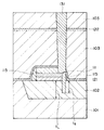
本発明の半導体装置に係る実施の形態の一例を、図1ないし図3はよって説明する。本発明の半導体装置は、DRAMメモリセルと周辺MOSトランジスタを有するものであり、図1では周辺MOSトランジスタの要部の概略構成断面図を示す。 An example of an embodiment of the semiconductor device according to the present invention will be described with reference to FIGS. The semiconductor device of the present invention has a DRAM memory cell and a peripheral MOS transistor, and FIG. 1 shows a schematic cross-sectional view of the main part of the peripheral MOS transistor.
図1に示すように、半導体基板101には素子分離絶縁膜102によって分離された素子形成領域にDRAMメモリセルと周辺MOSトランジスタが形成されている。上記周辺MOSトランジスタ領域のゲート電極111上と不純物拡散領域113とを覆うように絶縁膜からなる第1エッチングストッパ層121が形成されている。この第1のエッチングストッパ層121は例えばシリコン窒化膜からなる。また、DRAMメモリセルのキャパシタ部の上層には第2エッチングストッパ層122が、例えばシリコン窒化膜で形成されている。上記第2エッチングストッパ層122は、図示はしないが、DRAMメモリセルのキャパシタ部の下層、またはDRAMメモリセルのキャパシタ部の上層およびその下層に形成してもよい。なお、上記DRAMメモリセルや上記周辺MOSトランジスタの各層間には層間絶縁膜103が形成されている。
As shown in FIG. 1, a DRAM memory cell and a peripheral MOS transistor are formed in an element formation region isolated by an element
上記周辺MOSトランジスタの不純物拡散層113は、第2エッチングストッパ層122と第1エッチングストッパ層121を貫通する電極層131により、DRAMメモリセルのキャパシタ部上層に形成された金属配線層(図示せず)と接続されている。図示はしないが、上記周辺MOSトランジスタのゲート電極は、第2エッチングストッパ層122と第1エッチングストッパ層121を貫通する電極層により、DRAMメモリセルのキャパシタ部上層に形成された金属配線層と接続されている。
The impurity diffusion layer 113 of the peripheral MOS transistor is a metal wiring layer (not shown) formed on the upper layer of the capacitor portion of the DRAM memory cell by an
上記不純物拡散層の少なくとも一つの不純物拡散層113は、電極層131が該不純物拡散層113と素子分離絶縁膜102の境界上に接続されている。その素子分離絶縁膜102上に形成された電極層131の底部の不純物拡散層113表面からの深さ寸法tS は、不純物拡散層113の接合深さ寸法tJ もより短く形成されている。
In at least one impurity diffusion layer 113 of the impurity diffusion layer, the
上記第1エッチングストッパ層121は上記不純物拡散層113よりも薄く形成されるものであるから、素子分離絶縁膜102上に形成された電極層131の底部の不純物拡散層113表面からの深さ寸法tS は、第1エッチングストッパ層121の厚さt1 もより短く形成されてもよい。
Since the first
次に、本発明の半導体装置に係る実施の形態の一例を、図2よって説明する。本発明の半導体装置は、DRAMメモリセルと周辺MOSトランジスタを有するものであり、図2では周辺MOSトランジスタの要部の概略構成断面図を示す。 Next, an example of an embodiment according to the semiconductor device of the present invention will be described with reference to FIG. The semiconductor device of the present invention has a DRAM memory cell and a peripheral MOS transistor, and FIG. 2 shows a schematic cross-sectional view of the main part of the peripheral MOS transistor.
図2に示すように、半導体基板101には素子分離絶縁膜102によって分離された素子形成領域にDRAMメモリセルと周辺MOSトランジスタが形成されている。上記周辺MOSトランジスタ領域のゲート電極111上、このゲート電極111の側壁に形成されたサイドウォール115上、不純物拡散領域(図示せず)上等を覆うように絶縁膜からなる第1エッチングストッパ層121が形成されている。この第1のエッチングストッパ層121は例えばシリコン窒化膜からなる。また、DRAMメモリセルのキャパシタ部の上層には第2エッチングストッパ層122が、例えばシリコン窒化膜で形成されている。上記第2エッチングストッパ層122は、図示はしないが、DRAMメモリセルのキャパシタ部の下層、またはDRAMメモリセルのキャパシタ部の上層およびその下層に形成してもよい。なお、上記DRAMメモリセルや上記周辺MOSトランジスタの各層間には層間絶縁膜103が形成されている。
As shown in FIG. 2, DRAM memory cells and peripheral MOS transistors are formed in an element formation region separated by an element
上記DRAMメモリセル領域のワード・トランジスタ(図示せず)上には、周辺MOSトランジスタのサイドウォール形成層と第1エッチングストッパ層121が積層されて形成されている。上記周辺MOSトランジスタのゲート電極の少なくとも一つのゲート電極111は、電極層131が該ゲート電極111と上記サイドウォール形成層からなるサイドウォール絶縁膜115の境界上に接続されている。そのサイドウォール絶縁膜115上に形成された電極層131の底部の素子分離絶縁膜102上面からの深さ寸法tS は、素子分離絶縁膜102底部の深さ寸法tL もより短く形成されている。
On the word transistor (not shown) in the DRAM memory cell region, a sidewall forming layer of the peripheral MOS transistor and a first
上記図1、図2によって説明した半導体装置では、金属配線層から半導体基板101上に形成された不純物拡散層113、ゲート電極111等に接続するコンタクトを第2エッチングストッパ層122で一旦止め、かつ、不純物拡散層113、ゲート電極111等を覆う第1エッチングストッパ層121でエッチングを止めることにより形成することが可能となるので、半導体基板101のオーバエッチングが抑制されて接合リークが抑えられた構造となる。
In the semiconductor device described with reference to FIGS. 1 and 2, the contact connecting from the metal wiring layer to the impurity diffusion layer 113 formed on the
また、上記各半導体装置においては、上記周辺MOSトランジスタのサイドウォール形成層と上記第1エッチングストッパ層121の積層膜の膜厚は、上記DRAMメモリセル領域のワード・トランジスタの最小間隔の1/4以上かつ1/2以下、好ましくは、1/4以上かつ1/3以下としてある。
In each of the semiconductor devices, the thickness of the laminated film of the sidewall formation layer of the peripheral MOS transistor and the first
上記説明したように、第2エッチングストッパ層122が形成されていることから、DRAMセルの上層に形成した金属配線層から半導体基板上に形成された不純物拡散層とゲート電極に接続するコンタクトを形成する際にエッチングが第2エッチングストッパ層で一旦止まる。これにより、層間絶縁膜の膜厚ばらつきを一旦リセットできる。残りの層間絶縁膜の膜厚がより均一で、かつ、薄くなるので第1エッチングストッパ層121は第2エッチングストッパ層122よりもより薄く形成できる。したがって、第1エッチングストッパ層121を形成するDRAMセルの埋め込みにおいて、DRAMメモリセルで特にワード・トランジスタ間の埋め込み層間絶縁膜のボイド(空洞)の発生を防止できる。
As described above, since the second
また、DRAMセル下に形成するエッチングストッパは、DRAMセルのキャパシタと半導体基板101とを接続するコンタクトを形成する際のエッチング・マスクと兼用することが可能である。さらにDRAMセル下のエッチングストッパはシリンダー型キャパシタ形成時のエッチングストッパとも兼用が可能である。
The etching stopper formed under the DRAM cell can also be used as an etching mask for forming a contact for connecting the capacitor of the DRAM cell and the
さらに、上記DRAMメモリセル領域の第1エッチングストッパ層121上には熱処理により流動可能な酸化膜を層間絶縁膜として形成することにより、特にワード・トランジスタ間の埋め込み層間絶縁膜のボイド(空洞)の発生を防止できる。
Further, an oxide film that can flow by heat treatment is formed as an interlayer insulating film on the first
次に、本発明の半導体装置に係る実施の形態の一例を、図3よって説明する。本発明の半導体装置は、DRAMメモリセルと周辺MOSトランジスタを有するものであり、図3ではDRAMメモリセルビットコンタクトの要部を示し、(A)図に概略構成断面図を示し、(B)図に平面レイアウト図を示す。 Next, an example of an embodiment according to the semiconductor device of the present invention will be described with reference to FIG. The semiconductor device of the present invention has a DRAM memory cell and a peripheral MOS transistor. FIG. 3 shows a main part of a DRAM memory cell bit contact, FIG. 3 (A) shows a schematic sectional view, and FIG. Shows a plane layout diagram.
図3に示すように、半導体基板101には素子分離絶縁膜102によって分離された素子形成領域にDRAMメモリセルと周辺MOSトランジスタが形成されている。上記周辺MOSトランジスタ上を覆うように絶縁膜からなる第1エッチングストッパ層121が形成されている。この第1のエッチングストッパ層121は例えばシリコン窒化膜からなる。また、DRAMメモリセル領域にはビット線141が形成されている。さらにDRAMメモリセルのキャパシタ部の上層には第2エッチングストッパ層122が、例えばシリコン窒化膜で形成されている。上記第2エッチングストッパ層122は、図示はしないが、DRAMメモリセルのキャパシタ部の下層、またはDRAMメモリセルのキャパシタ部の上層およびその下層に形成してもよい。なお、上記DRAMメモリセルや上記周辺MOSトランジスタの各層間には層間絶縁膜103が形成されている。
As shown in FIG. 3, DRAM memory cells and peripheral MOS transistors are formed in an element formation region separated by an element
さらに、第2エッチングストッパ層122を貫通して上記DRAMメモリセル領域のビット線141に接続される電極層131が素子分離絶縁膜102上に配置されている。この電極層131は、本来、設計通りに形成されるならば、ビット線141上にのみ形成される。しかしながら、露光時の合わせずれ、加工誤差等により、図示されているように、ビット線141上よりはみ出して電極層131が接続される場合がある。このような構成であってもコンタクトが取れるような構成では、上記説明したように電極層131が素子分離絶縁膜102上に配置され、この電極層131の底部の素子分離絶縁膜102上面からの深さ寸法tSは、素子分離絶縁膜102底部の深さ寸法tL もより短く形成されている。
Further, an
次に、本発明の半導体装置に係る実施の形態の一例を、図4よって説明する。本発明の半導体装置は、DRAMメモリセルと周辺MOSトランジスタを有するものであり、図4ではDRAMメモリセルビットコンタクトの要部を示し、(A)図に概略構成断面図を示し、(B)図に平面レイアウト図を示す。 Next, an example of an embodiment according to the semiconductor device of the present invention will be described with reference to FIG. The semiconductor device of the present invention has a DRAM memory cell and a peripheral MOS transistor. FIG. 4 shows a main part of the DRAM memory cell bit contact, FIG. 4A shows a schematic cross-sectional view, and FIG. Shows a plane layout diagram.
図4に示すように、半導体基板101には素子分離絶縁膜102によって分離された不純物拡散領域105が形成されている。上記周辺MOSトランジスタ上を覆うように絶縁膜からなる第1エッチングストッパ層121が形成されている。この第1のエッチングストッパ層121は例えばシリコン窒化膜からなる。また、DRAMメモリセル領域にはビット線141が形成されている。さらにDRAMメモリセルのキャパシタ部の上層には第2エッチングストッパ層122が、例えばシリコン窒化膜で形成されている。上記第2エッチングストッパ層122は、図示はしないが、DRAMメモリセルのキャパシタ部の下層、またはDRAMメモリセルのキャパシタ部の上層およびその下層に形成してもよい。なお、上記DRAMメモリセルや上記周辺MOSトランジスタの各層間には層間絶縁膜103が形成されている。
As shown in FIG. 4, an
さらに、第2エッチングストッパ層122を貫通して上記DRAMメモリセル領域のビット線141に接続される電極層131が素子分離絶縁膜102上に配置されている。この電極層131は、本来、設計通りに形成されるならば、ビット線141上にのみ形成される。しかしながら、露光時の合わせずれ、加工誤差等により、図示されているように、ビット線141上よりはみ出して電極層131が接続される場合がある。このような構成であってもコンタクトが取れるような構成とするには、電極層131が上記ビット線141と同電位の不純物拡散領域105上に配置され、この電極層131の底部の不純物拡散領域105上面からの深さ寸法tS は、不純物拡散領域105の接合深さ寸法tJ より短く形成されている。
Further, an
上記図3、図4によって説明した半導体装置では、ビットコンタクトを第2エッチングストッパ層122で一旦止め、かつ、ビット線141をはみ出して形成された場合であっても、第1エッチングストッパ層121でエッチングを止めることが可能となるので、半導体基板101のオーバエッチングが抑制されて接合リークが抑えられた構造となる。
In the semiconductor device described with reference to FIGS. 3 and 4, even when the bit contact is temporarily stopped by the second
また、図3によって示した半導体装置では、電極層131が上記ビット線141と同電位の不純物拡散領域105上に配置され、この電極層131の底部の不純物拡散領域105上面からの深さ寸法tS は、不純物拡散領域105の接合深さ寸法tJ より短く形成されていることから、半導体基板101までビットコンタクトが突き抜けて形成されることはなく、したがって、電極層131は少なくとも不純物拡散領域105中で止まった状態で形成される。しかも、不純物拡散領域105はビット線141と同電位となっていることから、たとえビットコンタクトが不純物拡散総理105に接続されても、電気的影響はない。
In the semiconductor device shown in FIG. 3, the
また、図4によって示した半導体装置では、電極層131が素子分離絶縁膜102上に配置され、この電極層131の底部の素子分離絶縁膜102上面からの深さ寸法tS は、素子分離絶縁膜102底部の深さ寸法tL もより短く形成されていることから、半導体基板101までビットコンタクトが突き抜けて形成されることはなく、したがって、電極層131は少なくとも素子分離絶縁膜102中で止まった状態で形成される。
In the semiconductor device shown in FIG. 4, the
次に、本発明の半導体装置の製造方法に係る実施の形態の一例を以下に説明する。図5ないし図33は、本発明の一実施態様に基づく工程途中の装置断面図であり、図5から順に工程(1)から工程(29)まで製造途中の断面を模式的に表す。 Next, an example of an embodiment according to a method for manufacturing a semiconductor device of the present invention will be described below. 5 to 33 are sectional views of the apparatus in the middle of the process according to one embodiment of the present invention, and schematically show the sections in the middle of the production from step (1) to step (29) in order from FIG.
図5に示すように、P型のシリコン基板1に例えば50nm〜200nm(ここでは一例として100nm)のシリコン酸化膜2を形成した後、CVD(化学的気相成長)法を用いてシリコン窒化膜3を例えば100nm〜200nm(ここでは一例として150nm)の膜厚で重ねて形成する。シリコン酸化膜2はシリコン窒化膜3とシリコン基板1の間の応力を緩和するために形成する。シリコン窒化膜3のMOSトランジスタ等の素子形成領域上に選択的にフォトレジスト・パターン(図示せず)を形成する。シリコン窒化膜3、シリコン酸化膜2、シリコン基板1を順次エッチングして半導体素子分離領域となる溝部4を形成する。溝部4の深さは例えば250nm〜500nm(ここでは一例として350nm)の深さに設定する。
As shown in FIG. 5, after a silicon oxide film 2 of, for example, 50 nm to 200 nm (here, 100 nm as an example) is formed on a P-
図6に示すように、溝部4としシリコン窒化膜3を覆って、例えばHDP(高密度プラズマ)CVD(化学的気相成長)法によるシリコン酸化膜5を例えば500nm〜1000nm(ここでは一例として750nm)の膜厚で形成する。シリコン酸化膜5形成前に応力緩和を目的とした例えば50nm〜200nm(ここでは一例として100nm)程度のシリコン酸化膜(図示せず)を熱酸化法により形成してもよい。
As shown in FIG. 6, a trench 4 is formed to cover the silicon nitride film 3, and a
図7に示すように、CMP(化学的機械研磨)を用いて、素子分離領域となる溝部に埋め込んだシリコン酸化膜5を研磨して平坦化する。研磨後、シリコン窒化膜3とシリコン酸化膜2をエッチング除去する。本実施態様では、素子分離領域を溝部への埋め込み法で形成したが、従来から用いられているLOCOS法(選択酸化法)を用いてもよい。
As shown in FIG. 7, CMP (chemical mechanical polishing) is used to polish and planarize the
図8に示すように、例えば50nm〜200nm(ここでは一例として100nm)のシリコン酸化膜を酸化法により形成(図示せず)する。このシリコン酸化膜はいわゆる犠牲酸化膜として形成されるもので、この後、図8に示すイオン注入が実施された後に全て除去される。P型半導体基板1のDRAMメモリセル形成領域にN型不純物として例えばリンを高エネルギーで注入して、Nウエル領域6を形成し、そのNウエル領域6の内側にボロンをイオン注入してPウエル領域7を形成する。同時に、メモリセルの周辺に設けられるもので、メモリ機能と接続するロジック回路として機能する周辺MOS形成領域にもNウエル領域とPウエル領域を形成する。さらにNチャネルMOSトランジスタ、PチャネルMOSトランジスタ、DRAMメモリセルのワード・トランジスタのしきい値電圧を決定するイオン注入を行う。
As shown in FIG. 8, a silicon oxide film of, for example, 50 nm to 200 nm (here, 100 nm as an example) is formed by oxidation (not shown). This silicon oxide film is formed as a so-called sacrificial oxide film, and thereafter, all of the silicon oxide film is removed after the ion implantation shown in FIG. 8 is performed. For example, phosphorus is implanted as an N-type impurity at a high energy in the DRAM memory cell formation region of the P-
図9に示すように、50nm〜200nm(ここでは一例として100nm)のシリコン酸化膜(犠牲酸化膜)を除去した後、ゲート酸化膜を2〜10nmの厚さで形成する。このときトランジスタの用途に合わせてゲート酸化膜の膜厚を作り分ける。例えば、高電流駆動能力かつ低オフ電流が要求される周辺MOSトランジスタ形成領域では2nm〜5nm(ここでは一例として3nm)の薄膜ゲート酸化膜を形成する。一方、高電圧動作を要求される周辺MOSトランジスタ形成領域では5nm〜10nm(ここでは一例として6nm)の厚膜ゲート酸化膜を形成する。DRAMメモリセルのワード・トランジスタはセルのデータ保持能力に合わせたゲート酸化膜を設定することができる。このゲート酸化膜の作り分けは、より厚いゲート酸化膜を全面に形成した後に、薄いゲート酸化膜を形成する領域のゲート酸化膜を選択的にエッチング除去して再度酸化することにより形成できる。 As shown in FIG. 9, after removing the silicon oxide film (sacrificial oxide film) of 50 nm to 200 nm (here, 100 nm as an example), a gate oxide film is formed to a thickness of 2 to 10 nm. At this time, the thickness of the gate oxide film is made according to the use of the transistor. For example, a thin film gate oxide film of 2 nm to 5 nm (here, 3 nm as an example) is formed in a peripheral MOS transistor formation region where high current drive capability and low off current are required. On the other hand, a thick gate oxide film having a thickness of 5 nm to 10 nm (here, 6 nm as an example) is formed in the peripheral MOS transistor formation region requiring high voltage operation. For the word transistor of the DRAM memory cell, a gate oxide film can be set in accordance with the data retention capability of the cell. This gate oxide film can be formed by forming a thicker gate oxide film on the entire surface, then selectively removing the gate oxide film in the region where the thin gate oxide film is to be formed, and oxidizing it again.
ゲート電極としてポリシリコン層やアモルファス・シリコン層を50nm〜150nm(ここでは一例として100nm)の膜厚でCVD法やスパッタリングで形成する。この際、NチャネルMOSトランジスタ、PチャネルMOSトランジスタをいずれも表面チャネルのMOSで形成するデュアル・ゲート構造を採用する場合は、NチャネルMOSトランジスタ形成領域にはN型の不純物として例えばリンをイオン注入し、PチャネルMOSトランジスタ形成領域には例えばボロンをイオン注入する。ポリシリコン層またはアモルファス・シリコン層上に高融点金属シリサイド層である例えばタングステン・シリサイド層を50nm〜150nm(ここでは一例として100nm)の膜厚でCVD法やスパッタリングで形成する。 As the gate electrode, a polysilicon layer or an amorphous silicon layer is formed by CVD or sputtering with a film thickness of 50 nm to 150 nm (here, 100 nm as an example). At this time, when adopting a dual gate structure in which both the N channel MOS transistor and the P channel MOS transistor are formed by surface channel MOS, for example, phosphorus is ion-implanted as an N-type impurity in the N channel MOS transistor formation region. Then, for example, boron is ion-implanted into the P channel MOS transistor formation region. For example, a tungsten silicide layer, which is a refractory metal silicide layer, is formed on the polysilicon layer or the amorphous silicon layer with a film thickness of 50 nm to 150 nm (here, 100 nm as an example) by CVD or sputtering.
次にDRAMメモリセルの自己整合的コンタクトを形成する際のオフセット膜となる例えばシリコン窒化膜またはシリコン酸化膜を100nm〜200nm(ここでは一例として150nm)の膜厚でCVD法により形成する。ゲート電極パターンを形成するためのフォトレジスト・パターンを形成後、異方性エッチングによりオフセット膜と高融点金属シリサイド層とポリシリコン層またはアモルファス・シリコン層を順次エッチングしてゲート電極8パターンを形成する。
Next, for example, a silicon nitride film or a silicon oxide film serving as an offset film when forming a self-aligned contact of the DRAM memory cell is formed by a CVD method with a film thickness of 100 nm to 200 nm (here, 150 nm as an example). After forming the photoresist pattern for forming the gate electrode pattern, the offset film, the refractory metal silicide layer, the polysilicon layer or the amorphous silicon layer are sequentially etched by anisotropic etching to form the
図10に示すように、周辺MOSトランジスタ形成領域にLDD(ライトリー・ドープト・ドレイン)不純物拡散層9を形成する。NチャネルMOSトランジスタ形成領域にはN型の不純物例えば砒素をイオン注入し、PチャネルMOSトランジスタ形成領域には例えばボロン(BF2+)をイオン注入する。チャネル領域とLDD不純物拡散層9の間にポケット・イオン注入を行うことにより短チャネル効果を抑制することができる。例えば、NチャネルMOSトランジスタ形成領域にはP型の不純物例えばボロンをイオン注入し、PチャネルMOSトランジスタ形成領域には例えば砒素をイオン注入する。
As shown in FIG. 10, an LDD (lightly doped drain)
図11に示すように、一旦基板の全面にシリコン窒化膜を例えば40nm〜100nm(ここでは一例として60nm)の厚さに形成する。次に、周辺MOSトランジスタ形成領域にのみ開口部が形成されたフォトレジスト・パターン(図示せず)を形成する。次に、全面に異方性エッチングを行って不要なシリコン窒化膜を除去し、周辺MOSトランジスタ形成領域のゲート電極側壁にシリコン窒化膜のサイドウォール層10を形成する。
As shown in FIG. 11, a silicon nitride film is once formed on the entire surface of the substrate to a thickness of, for example, 40 nm to 100 nm (here, 60 nm as an example). Next, a photoresist pattern (not shown) having an opening formed only in the peripheral MOS transistor formation region is formed. Next, anisotropic etching is performed on the entire surface to remove unnecessary silicon nitride film, and a
図12に示すように、周辺MOSトランジスタ形成領域にソース・ドレイン不純物拡散層11を形成する。NチャネルMOSトランジスタ形成領域にはN型の不純物例えば砒素をイオン注入し、pチャネルMOSトランジスタ形成領域には例えばボロンをイオン注入する。DRAMメモリセル形成領域のワード・トランジスタとして例えばNチャネルMOSトランジスタを形成するためにN型の不純物例えばリンをイオン注入する。次に、シリコン基板上にコバルト層とチタン窒化膜を順次スパッタリングにより形成し、熱処理により、自己整合的にサイドウォール・シリコン窒化膜開口部にコバルト・シリサイド層12を形成する。サイドウォール・シリコン窒化膜上とオフセット膜上の未反応のコバルト層(図示せず)を除去する。
As shown in FIG. 12, source / drain impurity diffusion layers 11 are formed in the peripheral MOS transistor formation region. N-type impurities such as arsenic are ion-implanted into the N-channel MOS transistor formation region, and boron is ion-implanted into the p-channel MOS transistor formation region. In order to form, for example, an N-channel MOS transistor as a word transistor in the DRAM memory cell formation region, an N-type impurity such as phosphorus is ion-implanted. Next, a cobalt layer and a titanium nitride film are sequentially formed on the silicon substrate by sputtering, and a
図13に示すように、全面に第1エッチングストッパ層となるシリコン窒化膜(図示せず)を10nm〜50nm(ここでは一例として20nm)20nmの厚さに形成する。このときのシリコン窒化膜と下層のサイドウォールを形成した20nm〜100nm(ここでは一例として80nm)シリコン窒化膜サイドウォール層の積層膜厚合計は、30nm〜150nm(ここでは一例として100nm)になる。第1エッチングストッパ層となるシリコン窒化膜と下層のサイドウォールを形成したシリコン窒化膜の積層膜厚合計をDRAMメモリセル形成領域のワード・トランジスタ間距離である120nm〜450nmの1/4以上1/2以下、さらに効果を上げるためには1/4以上1/3以下にすることが望ましい。第1エッチングストッパ層となるシリコン窒化膜と下層のサイドウォールを形成したシリコン窒化膜の積層膜厚合計をDRAMメモリセル形成領域のワード・トランジスタ間距離の1/4以上1/2以下、さらに効果を上げるためには1/4以上1/3以下にすることによる効果を図34に示す。 As shown in FIG. 13, a silicon nitride film (not shown) serving as a first etching stopper layer is formed on the entire surface to a thickness of 20 nm to 10 nm to 50 nm (here, 20 nm as an example). At this time, the total laminated film thickness of the silicon nitride film side wall layer in which the silicon nitride film and the lower side wall are formed is 20 nm to 100 nm (in this example, 80 nm) is 30 nm to 150 nm (in this example, 100 nm). The total laminated film thickness of the silicon nitride film serving as the first etching stopper layer and the silicon nitride film on which the lower side wall is formed is equal to or more than ¼ of the word-transistor distance of 120 nm to 450 nm in the DRAM memory cell formation region. 2 or less, and in order to further increase the effect, it is desirable to set it to ¼ or more and 3 or less. The total laminated film thickness of the silicon nitride film serving as the first etching stopper layer and the silicon nitride film on which the lower side wall is formed is not less than ¼ and not more than ½ of the word-transistor distance in the DRAM memory cell formation region. FIG. 34 shows the effect obtained by setting it to 1/4 or more and 1/3 or less in order to increase the value.
図34に示すように、DRAMメモリセル形成領域のワード・トランジスタ間距離に対する、第1エッチングストッパ層となるシリコン窒化膜と下層のサイドウォールを形成したシリコン窒化膜の積層膜厚合計の割合を横軸に示し、縦軸にDRAMメモリセル形成領域のワード・トランジスタ間の埋め込み平坦化膜に発生するボイドによるコンタクト不良発生率と第1エッチングストッパ層の膜厚不足による接合リークによる不良発生率、通常、不良発生率は第1エッチングストッパ層の膜厚の絶対量で決まる。しかし、本発明で定義しているのは、第1エッチングストッパ層となるシリコン窒化膜と下層のサイドウォールを形成したシリコン地下膜の積層膜厚合計であるので、ワード・トランジスタ間距離である120nm〜450nmに対しては、その1/4以上が必要という相関関係が見られる。 As shown in FIG. 34, the ratio of the total film thickness of the silicon nitride film serving as the first etching stopper layer and the silicon nitride film forming the lower side wall to the word-transistor distance in the DRAM memory cell formation region is The vertical axis indicates the contact failure rate due to voids generated in the buried planarization film between the words and transistors in the DRAM memory cell formation region, and the failure rate due to junction leakage due to insufficient film thickness of the first etching stopper layer. The defect occurrence rate is determined by the absolute amount of the film thickness of the first etching stopper layer. However, what is defined in the present invention is the total film thickness of the silicon nitride film serving as the first etching stopper layer and the silicon base film formed with the lower side wall, so that the word-transistor distance is 120 nm. For ˜450 nm, there is a correlation indicating that ¼ or more is necessary.
図14に示すように、第1エッチングストッパ層上に500nm〜1000nm(ここでは一例として1000nm)程度の第1の層間絶縁膜13となるBPSG(ホウ素リンシリケートガラス)層をCVD法により形成し、前記第1の層間絶縁膜に650℃〜800℃(ここでは一例として700℃)の熱処理を加えてリフローすることにより平坦化する。このときDRAMメモリセル形成領域に形成した第1エッチングストッパ層となるシリコン窒化膜と下層のサイドウォールを形成したシリコン窒化膜の積層膜厚合計は最適な膜厚に設定されているので、前記第1の層間絶縁膜13であるBPSG膜の平坦化においてボイドが発生することは無い。
As shown in FIG. 14, a BPSG (boron phosphorus silicate glass) layer to be a first
この第1の層間絶縁膜はHDP(高密度プラズマ)CVD膜でもSOG(スピン・オン・グラス;塗布シリコン酸化膜)でも実施可能である。次にCMP(化学的機械研磨)により第1の層間絶縁膜13であるBPSG層を200nm〜900nm(ここでは一例として400nm)の厚さ分だけ研磨してさらに平坦化する。このときの平坦化は全面エッチバック等の技術を用いてもよい。
This first interlayer insulating film can be implemented by either an HDP (high density plasma) CVD film or an SOG (spin on glass; coated silicon oxide film). Next, the BPSG layer as the first
図15に示すように、DRAMメモリセル形成領域の第1の層間絶縁膜13に選択的にフォトレジスト開口パターンを形成し、第1エッチングストッパ層となるシリコン窒化膜と下層のサイドウォールを形成したシリコン窒化膜の積層膜厚と選択比の取れるエッチングで一旦エッチングを止め、続いてシリコン窒化膜の積層膜をエッチングしてDRAMメモリセルのワード線間に自己整合的にコンタクトホール14を形成する。この工程は、従来から一般的に用いられている自己整合コンタクト技術を用いて行う。
As shown in FIG. 15, a photoresist opening pattern was selectively formed in the first
コンタクトホール14内にポリシリコン層またはアモルファス・シリコン層を形成して、CMPによりコンタクトホール内のみに第1のシリコン電極層15を残す。本実施の形態では、CMPによる形成方法を用いたが、選択成長技術やエッチバックを用いてコンタクトホール14内に第1のシリコン電極層15を残してもよい。第1のシリコン電極層15に不純物を導入する方法は、第1のシリコン電極層15のCVDと同時に導入しても、CVD後のイオン注入により導入してもよい。本実施の形態では、DRAMメモリセルのNチャネルMOSで形成されるワード・トランジスタの不純物拡散層と接続する第1のシリコン電極層15を形成するのでN型の不純物であるリンを第1のシリコン電極層15に導入する。
A polysilicon layer or an amorphous silicon layer is formed in the
図16に示すように、シリコン酸化膜からなる第2の層間絶縁膜16を50nm〜200nm(ここでは一例として100nm)の膜厚で形成したのち、DRAMメモリセル形成領域に形成した第1のシリコン電極層のうちビットコンタクトに相当する第1のシリコン電極層の上に選択的に開口部を形成し、開口部を介して第1のシリコン電極層と接続されるビット線17を形成する。本実施の形態ではビット線17として50nm〜200nm(ここでは一例として150nm)の膜厚のタングステンおよび膜厚50nmのTiNバリアメタルの積層配線を用いたが、他の高融点金属や高融点金属シリサイド層とポリシリコンを積層させたポリサイド構造の配線を用いてもよい。また、ビット線は公知技術であるトリミング技術を用いてフォトリソグラフィーの解像限界以下の線幅に形成してもよい。
As shown in FIG. 16, after the second
図17に示すように、シリコン酸化膜からなる第3の層間絶縁膜18を500nm〜1500nm(ここでは一例として1000nm)の膜厚で形成した後、CMP、全面エッチバック等の技術を用いて平坦化する。次に第2エッチングストッパ層19となるシリコン窒化膜を50nm〜500nm(ここでは一例として300nm)の膜厚で形成する。このとき第2エッチングストッパ層19は下層に形成した第1エッチングストッパ層よりも厚く形成できる。
As shown in FIG. 17, after a third
DRAMメモリセル形成領域に形成した第1のシリコン電極層のうちキャパシタ電極に接続する第1のシリコン電極層の上におけるシリコン窒化膜に、開口部を選択的に形成する。開口部を覆って第4層間絶縁膜と第2エッチングストッパ層とエッチング選択比の取れる材料例えばポリシリコン層やアモルファス・シリコン層を50nm〜200nm(ここでは一例として80nm)の膜厚で全面に形成する。ポリシリコン層やアモルファス・シリコン層を異方性エッチングして第2のエッチングストッパ層の開口部側壁にポリシリコン層やアモルファス・シリコン層からなるサイドウォール・エッチング・マスク層を形成する。 An opening is selectively formed in the silicon nitride film on the first silicon electrode layer connected to the capacitor electrode in the first silicon electrode layer formed in the DRAM memory cell formation region. Covering the opening, the fourth interlayer insulating film, the second etching stopper layer, and a material having an etching selectivity such as a polysilicon layer or an amorphous silicon layer are formed over the entire surface with a thickness of 50 nm to 200 nm (here, 80 nm as an example). To do. The polysilicon layer or the amorphous silicon layer is anisotropically etched to form a sidewall etching mask layer made of the polysilicon layer or the amorphous silicon layer on the side wall of the opening of the second etching stopper layer.
図18に示すように、第2エッチングストッパ層19とサイドウォール・エッチング・マスク層21をエッチング・マスクとして第3の層間絶縁膜18をエッチングして、DRAMメモリセル形成領域に形成した第1のシリコン電極層15のうちキャパシタ電極に接続する第1のシリコン電極15にコンタクトホール20を形成する。このとき形成されるコンタクトホール20は、第2エッチングストッパ層19とその開口部に自己整合的に形成されたサイドウォール・エッチング・マスク層21を用いてエッチング形成されるので、リソグラフィー技術の限界を超えたコンタクト径のコンタクトホールが形成可能となる。それによって、上述したトリミングを利用したビット線形成技術を用いても、コンタクトがビット線より落ちることなく、またコンタクトホール20とビット線との耐圧が確保しやすくなる。
As shown in FIG. 18, the third
図19に示すように、コンタクトホール20内にポリシリコン層またはアモルファス・シリコン層を形成して、CMPによりコンタクトホール20内のみに第2のシリコン電極層22を残す。本実施の形態では、CMPによる形成方法を用いたが、選択成長技術やエッチバックを用いてコンタクトホール20内に第2のシリコン電極層22を残してもよい。第2のシリコン電極層22に不純物を導入する方法は、第2のシリコン電極層22のCVDと同時に導入しても、CVD後にイオン注入により導入してもよい。本実施の形態では、DRAMメモリセルのNチャネルMOSで形成されるワード・トランジスタの不純物拡散層と接続する第1のシリコン電極層15上に第2のシリコン電極層22を形成するのでN型の不純物であるリンを第2のシリコン電極層22に導入する。
As shown in FIG. 19, a polysilicon layer or an amorphous silicon layer is formed in the contact hole 20, and the second
図20に示すように、第2エッチングストッパ層19上に第2エッチングストッパ層19と第1のシリコン電極層22とエッチング選択比の取れるBPSG等の絶縁膜23を500nm〜1500nm(ここでは一例として1000nm)の膜厚で形成し、第2のシリコン電極層22上に開口部25を形成する。
As shown in FIG. 20, an insulating
図21に示すように、開口部にポリシリコン層またはアモルファス・シリコン層を形成して、CMPによりコンタクトホール(開口部)25内のみにキャパシタ下部電極となる第3のシリコン電極層24を残す。本実施の形態では、CMPによる形成方法を用いたが、反応性イオンエッチング(RIE)等のエッチバックを用いてコンタクトホール25内のみに第3のシリコン電極層24を残すことでもよい。第3のシリコン電極層24に不純物を導入する方法は、第3のシリコン電極層24のCVDと同時に導入しても、CVD後にイオン注入により導入してもよい。本実施の形態では、N型の不純物であるリンを第3のシリコン電極層24に導入する。
As shown in FIG. 21, a polysilicon layer or an amorphous silicon layer is formed in the opening, and the third silicon electrode layer 24 that becomes the capacitor lower electrode is left only in the contact hole (opening) 25 by CMP. In the present embodiment, the formation method by CMP is used, but the third silicon electrode layer 24 may be left only in the
図22に示すように、第2エッチバックストッパ層19と選択比の取れる等方性エッチングである例えばフッ酸を用いたウエット・エッチングにより、BPSG等の絶縁膜23を除去し、キャパシタ下部電極となる第3のシリコン電極層24が直立した構造を形成する。
As shown in FIG. 22, the insulating
図23に示すように、誘電体膜26としてONO膜(シリコン酸化膜−シリコン窒化膜−シリコン酸化膜)を3nm〜10nm(ここでは一例として5nm)の膜厚に形成する。さらにポリシリコン層またはアモルファス・シリコン層を形成してキャパシタ上部電極となる第4のシリコン電極層27を形成する。第4のシリコン電極層27に不純物を導入する方法は、第4のシリコン電極層27のCVDと同時に導入しても、CVD後にイオン注入により導入してもよい。本実施の形態では、N型の不純物であるリンを第4のシリコン電極層27に導入する。 As shown in FIG. 23, an ONO film (silicon oxide film-silicon nitride film-silicon oxide film) is formed as the dielectric film 26 to a thickness of 3 nm to 10 nm (here, 5 nm as an example). Further, a polysilicon layer or an amorphous silicon layer is formed to form a fourth silicon electrode layer 27 to be a capacitor upper electrode. As a method for introducing impurities into the fourth silicon electrode layer 27, the impurity may be introduced simultaneously with the CVD of the fourth silicon electrode layer 27 or by ion implantation after the CVD. In this embodiment mode, phosphorus that is an N-type impurity is introduced into the fourth silicon electrode layer 27.
本実施の形態では、キャパシタ電極としてシリコン電極を用いたが、金属電極を用いてもよい。さらに本実施の形態ではキャパシタ誘電体膜26としてONO膜を用いたが、タンタル酸化膜やBST等の強誘電体膜を用いてもよい。さらに、本発明の実施の形態では、シリンダー構造のキャパシタを形成したが、単純な積層型キャパシタやフィン構造のキャパシタ電極でも適用可能である。第2エッチングストッパ層と選択比の取れる等方性エッチングで第3のシリコン電極層24下におけるBPSG等の絶縁膜23を除去する際と、第4のシリコン電極層27パターンをエッチング形成する際に、第2のエッチングストッパ層19がエッチングされて膜厚が減少する。このときの膜減り量のコントロールが困難な場合には、第4のシリコン電極層27パターンをエッチング形成する際に第2エッチングストッパ層19の全膜厚の一部または全部をエッチング除去して、新たに第3エッチングストッパ層を形成する製造方法を他の本発明による半導体装置の製造方法とする。
In this embodiment, a silicon electrode is used as the capacitor electrode, but a metal electrode may be used. Further, in the present embodiment, an ONO film is used as the capacitor dielectric film 26, but a ferroelectric film such as a tantalum oxide film or BST may be used. Further, in the embodiment of the present invention, the capacitor having the cylinder structure is formed, but a simple multilayer capacitor or a capacitor electrode having a fin structure can be applied. When the insulating
第24図に示すように、シリコン酸化膜からなる第4の層間絶縁膜28を500nm〜2500nm(ここでは一例として1500nm)の膜厚で形成したのち、CMPやエッチバック等の技術を用いてキャパシタ上に第4の層間絶縁膜が100nm〜1000nm(ここでは一例として1000nm)の厚さが残るように平坦化する。
As shown in FIG. 24, after a fourth
図25に示すように、第4の層間絶縁膜28上に選択的にフォトレジスト開口パターン29を形成する。
As shown in FIG. 25, a
本実施の形態では周辺MOSトランジスタ形成領域のゲート電極配線上へのコンタクトホール30をまず開口する。第4の層間絶縁膜28をエッチングするこのとき第2エッチングストッパ層19と選択比の取れるエッチング条件により、第4の層間絶縁膜28を除去後、第2エッチングストッパ層19上でエッチングを一旦止める。
In this embodiment, a
図26に示すように、第2エッチングストッパ層19をエッチングして、さらに第3の層間絶縁膜18と第2の層間絶縁膜16と第1の層間絶縁膜13を順次エッチングする。このとき第1エッチングストッパ層と選択比の取れるエッチング条件により、第1の層間絶縁膜13を除去した後、第1エッチングストッパ層上でエッチングを一旦止める。
As shown in FIG. 26, the second
図27に示すように、第1エッチングストッパ層13をエッチングして、次に周辺MOSトランジスタ形成領域のゲート電極8のオフセット膜(例えばシリコン窒化膜またはシリコン酸化膜)をエッチング除去して、ゲート電極8上にコンタクトホール30を形成する。
As shown in FIG. 27, the first
図36に示すように、本図は、本発明の構成において、エッチングストッパ層を貫通するコンタクト窓30内に形成される電極層(図示せず)がゲート電極8とゲート電極8の側壁に形成されたサイドウォール絶縁膜の境界上に接続された場合の素子分離絶縁膜5の掘れ量低減効果を示す図であり、図中tS は素子分離絶縁膜5上に形成された電極底部の深さ寸法、tL は素子分離絶縁膜5底部の深さ寸法である。
As shown in FIG. 36, in this figure, in the configuration of the present invention, an electrode layer (not shown) formed in the
図28に示すように、第4の層間絶縁膜28条に選択的にフォトレジスト開口パターン31を形成する。
As shown in FIG. 28, a
本実施の形態では、周辺MOSトランジスタ形成領域のゲート電極8配線層上へのコンタクト30に続いて、周辺MOSトランジスタ形成領域の不純物拡散層上にコンタクトホール32を開口する。この時、ゲート電極8上に形成したコンタクトホール30上はフォトレジスト31で埋め込まれる。第4の層間絶縁膜28をエッチングするとき第2エッチングストッパ層19と選択比の取れるエッチング条件により、第4の層間絶縁膜28を除去後、第2エッチングストッパ19層上でエッチングを一旦止める。
In the present embodiment, a
図29に示すように、第2エッチングストッパ層19をエッチングして、さらに第3の層間絶縁膜18と第2の層間絶縁膜16と第1の層間絶縁膜13を順次エッチングする。このとき第1エッチングストッパ層と選択比の取れるエッチング条件により、第1の層間絶縁膜13を除去した後、第1エッチングストッパ層上でエッチングを一旦止める。
As shown in FIG. 29, the second
図30に示すように、第1エッチングストッパ層をエッチングして、周辺MOSトランジスタ形成領域の不純物拡散層上にコンタクトホール32を形成する。
As shown in FIG. 30, the first etching stopper layer is etched to form a
図31に示すように、コンタクトホール32内に、例えば10nm〜100nm(ここでは一例として20nm)の厚さのチタン層と、例えば10nm〜50nm(ここでは一例として20nm)20nmの厚さのバリアメタルとなる窒化チタン膜をスパッタリングまたはCVD法により形成する。次に、第1の金属電極となるタングステン層33を例えば100nm〜500nm(ここでは一例として300nm)の膜厚に、スパッタリングまたはCVD法により形成する。次いでCMPもしくは全面エッチバックによりコンタクトホール32内にのみ第1の金属電極33を残すように他の領域から第1の金属電極33を除去する。第1の金属電極33は、選択CVD法等の技術を用いて、コンタクトホール32内に当初より選択形成すれば、エッチバックやCMPの工程が省ける。
As shown in FIG. 31, in the
図32に示すように、第1の金属電極33と電気的に接続される、第1層目金属配線層34を形成する。第1層目金属配線層34は、例えば、3nm〜50nmの厚さのチタン層、10nm〜50nm(ここでは一例として10nm)の厚さのバリアメタルとなるチタン窒化膜、200nm〜800nm(ここでは一例として400nm)の厚さの銅を含有するアルミニウム配線層、3nm〜10nm(ここでは一例として5nm)の厚さのチタン層、10nm〜100nm(ここでは一例として70nmの厚さのチタン窒化膜を、スパッタリングもしくはCVD法によって形成する。銅を含有するアルミニウム配線層は、アルミニウム配線や銅配線などの他の材料でもよい。第1層目金属配線層34上に第5の層間絶縁膜35となるシリコン酸化膜を500nm〜2000nm(ここでは一例として2000nm)の膜厚で形成した後、CMP等を用いて行うエッチバックを用いて平坦化する。
As shown in FIG. 32, a first metal wiring layer 34 that is electrically connected to the first metal electrode 33 is formed. The first metal wiring layer 34 is, for example, a titanium layer with a thickness of 3 nm to 50 nm, a titanium nitride film serving as a barrier metal with a thickness of 10 nm to 50 nm (here 10 nm as an example), 200 nm to 800 nm (here As an example, an aluminum wiring layer containing copper having a thickness of 400 nm, a titanium layer having a thickness of 3 nm to 10 nm (here 5 nm as an example), and a titanium nitride film having a thickness of 10 nm to 100 nm (here 70 nm as an example). The aluminum wiring layer containing copper may be other materials such as aluminum wiring and copper wiring, etc. The fifth
図33は図32に対応する工程に続く工程での装置断面を示している。図33に示すように、第1の金属電極33と第1層目金属配線層34と第5の層間絶縁膜35の形成と同様にして、第2の金属電極36と第2層目金属配線層37と第6の層間絶縁膜38、第3の金属電極39と第3層目金属配線層40と第7の層間絶縁膜41、第4の金属電極42と第4層目金属配線層43と第8の層間絶縁膜44を順次形成する。オーバーコート膜45としてシリコン窒化膜を例えば500nm〜1500nm(ここでは一例として700nm)の厚さに形成した後、第4層目金属配線層43でパッドとなる部分に開口部(図示せず)を選択的に形成する。
FIG. 33 shows a cross section of the device in a step that follows the step corresponding to FIG. As shown in FIG. 33, the
本実施の形態では、周辺MOSトランジスタ形成領域のゲート電極層上へのコンタクトホールと不純物拡散層上にコンタクトホールを別々に開口する方法を説明したが、同時に一括して開口することも可能である。別々に開口する場合、その開口順序は、不純物拡散層上から先に開口し、続いてゲート電極配線上に開口することも可能である。 In the present embodiment, the method of separately opening the contact hole on the gate electrode layer and the impurity diffusion layer in the peripheral MOS transistor formation region has been described. However, it is also possible to simultaneously open the contact hole. . In the case of opening separately, the opening order may be such that the impurity diffusion layer is opened first and then the gate electrode wiring is opened.
本発明の実施の形態によれば、図35に示すように、金属配線層と接続される電極層が埋め込まれる開口部は、例えば不純物拡散層と素子分離絶縁膜の境界上に形成されても、第2エッチングストッパ層と第1エッチングストッパ層とによりエッチングが制御(一旦停止)されているので、素子分離絶縁膜の掘れ量tSが不純物拡散層の接合深さ寸法tJ より大きくなることはない。このため、接合リークの低減化が可能となる。また、第1エッチングストッパ層の膜厚t1 はDRAMメモリセルの埋め込みが可能な、必要最小限の膜厚に設定しており、第1エッチングストッパ層のエッチング時におけるオーバエッチング量に相当する素子分離絶縁膜の掘れ量tS よりも第1エッチングストッパ層の膜厚寸法t1 は大きくなる。 According to the embodiment of the present invention, as shown in FIG. 35, the opening in which the electrode layer connected to the metal wiring layer is embedded may be formed on the boundary between the impurity diffusion layer and the element isolation insulating film, for example. Since the etching is controlled (temporarily stopped) by the second etching stopper layer and the first etching stopper layer, the digging amount t S of the element isolation insulating film is larger than the junction depth dimension t J of the impurity diffusion layer. There is no. For this reason, junction leakage can be reduced. Further, the film thickness t 1 of the first etching stopper layer is set to a minimum necessary film thickness that can be embedded in the DRAM memory cell, and an element corresponding to the overetching amount at the time of etching the first etching stopper layer. The film thickness dimension t 1 of the first etching stopper layer is larger than the digging amount t S of the isolation insulating film.
比較例として、本発明の構造と方法を採用していない例を図37によって説明する。図37に示すように、素子分離絶縁膜の掘れ量tS が不純物拡散層の接合深さ寸法tJ より大きくなると、金属配線層と接続される電極層を介して不純物拡散層とウエル領域がショートする。 As a comparative example, an example in which the structure and method of the present invention are not employed will be described with reference to FIG. As shown in FIG. 37, when the digging amount t S of the element isolation insulating film becomes larger than the junction depth dimension t J of the impurity diffusion layer, the impurity diffusion layer and the well region are connected via the electrode layer connected to the metal wiring layer. Short circuit.
本発明の実施の形態によれば、図36に示すように、金属配線層と接続される電極層が埋め込まれる開口部は、例えばゲート電極層とサイドウォール絶縁膜の境界上に形成されても、第2エッチングストッパ層と第1エッチングストッパ層とによりエッチングが制御されているので、素子分離絶縁膜の掘れ量tS が素子分離絶縁膜の深さ寸法tL より大きくなることはない。 According to the embodiment of the present invention, as shown in FIG. 36, the opening in which the electrode layer connected to the metal wiring layer is embedded may be formed on the boundary between the gate electrode layer and the sidewall insulating film, for example. Since the etching is controlled by the second etching stopper layer and the first etching stopper layer, the digging amount t S of the element isolation insulating film does not become larger than the depth dimension t L of the element isolation insulating film.
比較例として、本発明の構造と方法を採用していない例を図38によって説明する。図38に示すように、素子分離絶縁膜の掘れ量tS が素子分離絶縁膜の深さ寸法tL より大きくなると、金属配線層と接続される電極層を介してゲート電極とウエル領域がショートする。 As a comparative example, an example in which the structure and method of the present invention are not employed will be described with reference to FIG. As shown in FIG. 38, when the digging amount t S of the element isolation insulating film becomes larger than the depth dimension t L of the element isolation insulating film, the gate electrode and the well region are short-circuited via the electrode layer connected to the metal wiring layer. To do.
以上が、一実施の形態に基づく本発明の説明であるが、これに限らず本発明には種々の変形が可能である。例えば、周辺MOSトランジスタとしては、メモリセルの周辺に設けメモリ機能と接続するロジック回路を構成するMOSトランジスタをレイアウトとして取り上げて説明したが、このようなものだけにとどまらず、メモリセル以外におけるDRAM自体の機能の一部を成すMOSトランジスタや、SRAMセルを構成するMOSトランジスタ等、DRAMメモリ部分とは異なり構成要素の標高が比較的低いMOSトランジスタであれば何でも同様の効果を得ることができる。 The above is the description of the present invention based on one embodiment. However, the present invention is not limited to this, and various modifications can be made to the present invention. For example, as the peripheral MOS transistor, the MOS transistor constituting the logic circuit provided around the memory cell and connected to the memory function has been described as a layout. However, the peripheral MOS transistor is not limited to this, but the DRAM itself other than the memory cell Unlike a DRAM memory portion, such as a MOS transistor that forms a part of the above functions and a MOS transistor that constitutes an SRAM cell, the same effect can be obtained with any MOS transistor having a relatively low altitude.
また、第2エッチバックストッパ膜の形成位置としては、(1)ワード線の直上に設けられる層間絶縁膜とビット線部分に設けられる層間絶縁膜との間に設ける方法、(2)キャパシタ形成前(ビット線部分に設けられる層間絶縁膜の上)に設ける方法、(3)キャパシタ形成後(ビット線部分に設けられる層間絶縁膜の上)に設ける方法による三ヶ所いずれでもよい。 The second etch-back stopper film can be formed by (1) a method provided between an interlayer insulating film provided immediately above the word line and an interlayer insulating film provided on the bit line portion, and (2) before capacitor formation. Any of the three methods may be used (a method provided on the interlayer insulating film provided on the bit line portion) and (3) a method provided on the interlayer insulating film provided on the bit line portion after the capacitor is formed.
また、上記の実施の形態において、近接するメモリセルトランジスタのゲート(ワード線)相互間のボイドを埋めることを例示して説明しているが、本発明はワード線以外のゲート電極、配線層等同様に異方性エッチバックにてパターニングされる各種パターンの相互間にできる凹部を埋めるのに好ましく用いることができ、適用できるものはワード線間だけにとどまらない。 In the above embodiment, the description has been given by exemplifying filling of voids between the gates (word lines) of adjacent memory cell transistors. However, the present invention is applied to gate electrodes other than word lines, wiring layers, and the like. Similarly, it can be preferably used to fill a concave portion formed between various patterns patterned by anisotropic etch back, and applicable ones are not limited to between word lines.
また、エッチバックストッパの材料としては、シリコン窒化膜を用いる以外にも、適宜、層間絶縁膜の種類と開口時に用いるエッチャントガスの種類とを検討して用いることができるが、一般的には絶縁膜を用いるべきであろう。導電膜を用いた場合には、エッチングストッパ膜として用済み後の除去が必須となるが、その除去が容易ではなく、仮に異方性エッチング等で除去しようとしても段差下や側壁の脇などにどうしても除去されずに残ることがあり、後の工程で残余の導電膜がショートを起こす原因を作る場合がある。また絶縁膜材料からエッチングストッパとして用いることができるものを選択するにも、微細化した最近の半導体装置内部に用いるには、高速性能を損なわないように、また配線間容量を下げられるように、比誘電率が低い材料からの選択が好ましい。 In addition to using a silicon nitride film, the etch-back stopper material can be appropriately determined by considering the type of interlayer insulating film and the type of etchant gas used at the time of opening. A membrane should be used. When a conductive film is used, removal after use as an etching stopper film is indispensable, but it is not easy to remove. In some cases, the conductive film may remain without being removed, and may cause a short circuit of the remaining conductive film in a later process. In addition, in order to select an insulating film material that can be used as an etching stopper, in order to use it in a recent miniaturized semiconductor device, so as not to impair high-speed performance and to reduce the capacitance between wirings. Selection from a material with a low dielectric constant is preferred.
次に、以下に、上記説明した実施の形態の他に、本発明の主要な実施の形態についてまとめておく。 Next, in addition to the above-described embodiments, the main embodiments of the present invention are summarized below.
(1)半導体装置は、DRAMメモリセルと周辺MOSトランジスタを有するものであり、上記周辺MOSトランジスタのゲート電極を含む表面を覆うように第1エッチングストッパ層となる絶縁膜が形成されている。また、上記DRAMメモリセルのキャパシタ部の上層ないし下層のうちの少なくとも一方には、第2エッチングストッパ層が形成されている。上記周辺MOSトランジスタの不純物拡散層とゲート電極は、上記第1エッチングストッパ層と上記第2エッチングストッパ層を貫通する電極層により、DRAMメモリセルのキャパシタ部上層に形成されている金属配線層と接続されている。そして上記不純物拡散層の少なくとも一つは、上記電極層が該不純物拡散層と素子分離絶縁膜の境界上に接続され、素子分離絶縁膜上に形成された電極層の底部の不純物拡散層表面からの深さ寸法は、不純物拡散層の接合深さ寸法よりも小さく形成されていることが特徴となっている。 (1) The semiconductor device has a DRAM memory cell and a peripheral MOS transistor, and an insulating film serving as a first etching stopper layer is formed so as to cover the surface including the gate electrode of the peripheral MOS transistor. A second etching stopper layer is formed on at least one of the upper layer and the lower layer of the capacitor portion of the DRAM memory cell. The impurity diffusion layer and the gate electrode of the peripheral MOS transistor are connected to a metal wiring layer formed on the upper layer of the capacitor portion of the DRAM memory cell by an electrode layer passing through the first etching stopper layer and the second etching stopper layer. Has been. At least one of the impurity diffusion layers is formed by connecting the electrode layer on the boundary between the impurity diffusion layer and the element isolation insulating film, from the surface of the impurity diffusion layer at the bottom of the electrode layer formed on the element isolation insulating film. The depth dimension is characterized by being formed smaller than the junction depth dimension of the impurity diffusion layer.
(2)半導体装置は、DRAMメモリセルと周辺MOSトランジスタを有するものであり、上記周辺MOSトランジスタのゲート電極を含む表面を覆うように第1エッチングストッパ層となる絶縁膜が形成されている。また、上記DRAMメモリセルのキャパシタ部の上層ないし下層のうちの少なくとも一方には、第2エッチングストッパ層が形成されている。上記周辺MOSトランジスタの不純物拡散層とゲート電極は、上記第1エッチングストッパ層と上記第2エッチングストッパ層を貫通する電極層により、DRAMメモリセルのキャパシタ部上層に形成されている金属配線層と接続されている。そして上記不純物拡散層の少なくとも一つは、上記電極層が該不純物拡散層と素子分離絶縁膜の境界上に接続され、素子分離絶縁膜上に形成された電極層の底部の不純物拡散層表面からの深さ寸法は、第1エッチングストッパ層の厚さ寸法よりも小さく形成されていることが特徴となっている。 (2) The semiconductor device has a DRAM memory cell and a peripheral MOS transistor, and an insulating film serving as a first etching stopper layer is formed so as to cover the surface including the gate electrode of the peripheral MOS transistor. A second etching stopper layer is formed on at least one of the upper layer and the lower layer of the capacitor portion of the DRAM memory cell. The impurity diffusion layer and the gate electrode of the peripheral MOS transistor are connected to a metal wiring layer formed on the upper layer of the capacitor portion of the DRAM memory cell by an electrode layer passing through the first etching stopper layer and the second etching stopper layer. Has been. At least one of the impurity diffusion layers is formed by connecting the electrode layer on the boundary between the impurity diffusion layer and the element isolation insulating film, from the surface of the impurity diffusion layer at the bottom of the electrode layer formed on the element isolation insulating film. The depth dimension is characterized by being formed smaller than the thickness dimension of the first etching stopper layer.
(3)半導体装置は、DRAMメモリセルと周辺MOSトランジスタを有するものであり、上記周辺MOSトランジスタのゲート電極を含む表面を覆うように第1エッチングストッパ層となる絶縁膜が形成されている。また、上記DRAMメモリセルのキャパシタ部の上層ないし下層のうちの少なくとも一方には、第2エッチングストッパ層が形成されている。上記周辺MOSトランジスタの不純物拡散層とゲート電極は、上記第1エッチングストッパ層と上記第2エッチングストッパ層を貫通する電極層により、DRAMメモリセルのキャパシタ部上層に形成されている金属配線層と接続されている。そしてDRAMメモリセル領域のワード・トランジスタ上には、周辺MOSトランジスタのサイドウォール形成層と第1エッチングストッパ層が積層されて形成されている。さらに、周辺MOSトランジスタのサイドウォール形成層と第1エッチングストッパ層の積層膜の膜厚は、DRAMメモリセル領域のワード・トランジスタの最小間隔の1/4以上かつ1/2以下となっていることを特徴としている。 (3) The semiconductor device has a DRAM memory cell and a peripheral MOS transistor, and an insulating film serving as a first etching stopper layer is formed so as to cover the surface including the gate electrode of the peripheral MOS transistor. A second etching stopper layer is formed on at least one of the upper layer and the lower layer of the capacitor portion of the DRAM memory cell. The impurity diffusion layer and the gate electrode of the peripheral MOS transistor are connected to a metal wiring layer formed on the upper layer of the capacitor portion of the DRAM memory cell by an electrode layer passing through the first etching stopper layer and the second etching stopper layer. Has been. A sidewall formation layer of the peripheral MOS transistor and a first etching stopper layer are laminated on the word transistor in the DRAM memory cell region. Furthermore, the thickness of the laminated film of the sidewall formation layer of the peripheral MOS transistor and the first etching stopper layer is not less than 1/4 and not more than 1/2 of the minimum distance between the word transistors in the DRAM memory cell region. It is characterized by.
(4)半導体装置は、DRAMメモリセルと周辺MOSトランジスタを有するものであり、上記周辺MOSトランジスタのゲート電極を含む表面を覆うように第1エッチングストッパ層となる絶縁膜が形成されている。また、上記DRAMメモリセルのキャパシタ部の上層ないし下層のうちの少なくとも一方には、第2エッチングストッパ層が形成されている。上記周辺MOSトランジスタの不純物拡散層とゲート電極は、上記第1エッチングストッパ層と上記第2エッチングストッパ層を貫通する電極層により、DRAMメモリセルのキャパシタ部上層に形成されている金属配線層と接続されている。そしてDRAMメモリセル領域のワード・トランジスタ上には、周辺MOSトランジスタのサイドウォール形成層と第1エッチングストッパ層が積層されて形成されている。さらに、周辺MOSトランジスタのサイドウォール形成層と第1エッチングストッパ層の積層膜の膜厚は、DRAMメモリセル領域のワード・トランジスタの最小間隔の1/4以上かつ1/3以下となっていることを特徴としている。 (4) The semiconductor device has a DRAM memory cell and a peripheral MOS transistor, and an insulating film serving as a first etching stopper layer is formed so as to cover the surface including the gate electrode of the peripheral MOS transistor. A second etching stopper layer is formed on at least one of the upper layer and the lower layer of the capacitor portion of the DRAM memory cell. The impurity diffusion layer and the gate electrode of the peripheral MOS transistor are connected to a metal wiring layer formed on the upper layer of the capacitor portion of the DRAM memory cell by an electrode layer passing through the first etching stopper layer and the second etching stopper layer. Has been. A sidewall formation layer of the peripheral MOS transistor and a first etching stopper layer are laminated on the word transistor in the DRAM memory cell region. Furthermore, the thickness of the laminated film of the sidewall formation layer of the peripheral MOS transistor and the first etching stopper layer is not less than 1/4 and not more than 1/3 of the minimum distance between the word transistors in the DRAM memory cell region. It is characterized by.
(5)上記(3)で説明したDRAMメモリセルと周辺MOSトランジスタを有する半導体装置において、上記周辺MOSトランジスタのゲート電極を含む表面を覆うように第1エッチングストッパ層となる絶縁膜が形成されている。また、上記DRAMメモリセルのキャパシタ部の上層ないし下層のうちの少なくとも一方には、第2エッチングストッパ層が形成されている。そしてDRAMメモリセル領域のワード・トランジスタ上には、周辺MOSトランジスタのサイドウォール形成層と第1エッチングストッパ層が積層されて形成されている。さらに、周辺MOSトランジスタのサイドウォール形成層と第1エッチングストッパ層の積層膜の膜厚は、DRAMメモリセル領域のワード・トランジスタの最小間隔の1/4以上かつ1/2以下となっていることを特徴としている。 (5) In the semiconductor device having the DRAM memory cell and the peripheral MOS transistor described in (3) above, an insulating film serving as a first etching stopper layer is formed so as to cover the surface including the gate electrode of the peripheral MOS transistor. Yes. A second etching stopper layer is formed on at least one of the upper layer and the lower layer of the capacitor portion of the DRAM memory cell. A sidewall formation layer of the peripheral MOS transistor and a first etching stopper layer are laminated on the word transistor in the DRAM memory cell region. Furthermore, the thickness of the laminated film of the sidewall formation layer of the peripheral MOS transistor and the first etching stopper layer is not less than 1/4 and not more than 1/2 of the minimum distance between the word transistors in the DRAM memory cell region. It is characterized by.
(6)半導体装置は、DRAMメモリセルと周辺MOSトランジスタを有するものであり、上記周辺MOSトランジスタのゲート電極を含む表面を覆うように第1エッチングストッパ層となる絶縁膜が形成されている。また、上記DRAMメモリセルのキャパシタ部の上層ないし下層のうちの少なくとも一方には、第2エッチングストッパ層が形成されている。上記周辺MOSトランジスタの不純物拡散層とゲート電極は、上記第1エッチングストッパ層と上記第2エッチングストッパ層を貫通する電極層により、DRAMメモリセルのキャパシタ部上層に形成されている金属配線層と接続されている。そして周辺MOSトランジスタのゲート電極の少なくとも一つは、上記エッチングストッパ層を貫通する電極層が上記ゲート電極と上記ゲート電極側壁に形成されてサイドウォール絶縁膜の境界上に接続されている。さらに上記サイドウォール絶縁膜上に形成された上記電極層の底部の素子分離絶縁膜上面からの深さ寸法は、上記素子分離絶縁膜底部の深さ寸法よりも小さく形成されたことを特徴としている。 (6) The semiconductor device has a DRAM memory cell and a peripheral MOS transistor, and an insulating film serving as a first etching stopper layer is formed so as to cover the surface including the gate electrode of the peripheral MOS transistor. A second etching stopper layer is formed on at least one of the upper layer and the lower layer of the capacitor portion of the DRAM memory cell. The impurity diffusion layer and the gate electrode of the peripheral MOS transistor are connected to a metal wiring layer formed on the upper layer of the capacitor portion of the DRAM memory cell by an electrode layer passing through the first etching stopper layer and the second etching stopper layer. Has been. At least one of the gate electrodes of the peripheral MOS transistor has an electrode layer penetrating the etching stopper layer formed on the gate electrode and the side wall of the gate electrode and connected to the boundary of the side wall insulating film. Further, the depth dimension from the upper surface of the element isolation insulating film at the bottom of the electrode layer formed on the sidewall insulating film is smaller than the depth dimension of the bottom of the element isolation insulating film. .
(7)上記(1)で説明したDRAMメモリセルと周辺MOSトランジスタを有する半導体装置において、上記第2エッチングストッパ層の膜厚は上記第1エッチングストッパ層の膜厚よりも厚く形成されていることが特徴となっている。 (7) In the semiconductor device having the DRAM memory cell and the peripheral MOS transistor described in (1) above, the film thickness of the second etching stopper layer is formed larger than the film thickness of the first etching stopper layer. Is a feature.
(8)上記(2)で説明したDRAMメモリセルと周辺MOSトランジスタを有する半導体装置において、上記第2エッチングストッパ層の膜厚は上記第1エッチングストッパ層の膜厚よりも厚く形成されていることが特徴となっている。 (8) In the semiconductor device having the DRAM memory cell and the peripheral MOS transistor described in (2) above, the film thickness of the second etching stopper layer is formed larger than the film thickness of the first etching stopper layer. Is a feature.
(9)上記(3)で説明したDRAMメモリセルと周辺MOSトランジスタを有する半導体装置において、上記第2エッチングストッパ層の膜厚は上記第1エッチングストッパ層の膜厚よりも厚く形成されていることが特徴となっている。 (9) In the semiconductor device having the DRAM memory cell and the peripheral MOS transistor described in (3) above, the second etching stopper layer is formed to be thicker than the first etching stopper layer. Is a feature.
(10)上記(4)で説明したDRAMメモリセルと周辺MOSトランジスタを有する半導体装置において、上記第2エッチングストッパ層の膜厚は上記第1エッチングストッパ層の膜厚よりも厚く形成されていることが特徴となっている。 (10) In the semiconductor device having the DRAM memory cell and the peripheral MOS transistor described in (4) above, the second etching stopper layer is formed to be thicker than the first etching stopper layer. Is a feature.
(11)上記(5)で説明したDRAMメモリセルと周辺MOSトランジスタを有する半導体装置において、上記第2エッチングストッパ層の膜厚は上記第1エッチングストッパ層の膜厚よりも厚く形成されていることが特徴となっている。 (11) In the semiconductor device having the DRAM memory cell and the peripheral MOS transistor described in (5) above, the second etching stopper layer is formed to be thicker than the first etching stopper layer. Is a feature.
(12)上記(6)で説明したDRAMメモリセルと周辺MOSトランジスタを有する半導体装置において、上記第2エッチングストッパ層の膜厚は上記第1エッチングストッパ層の膜厚よりも厚く形成されていることが特徴となっている。 (12) In the semiconductor device having the DRAM memory cell and the peripheral MOS transistor described in (6) above, the second etching stopper layer is formed to be thicker than the first etching stopper layer. Is a feature.
(13)半導体装置の製造方法は、DRAMメモリセルと周辺MOSトランジスタを有する半導体装置の製造方法であって、素子分離絶縁膜と素子形成領域が形成された半導体基板上に上記DRAMメモリセルのワード・トランジスタと上記周辺MOSトランジスタを形成する工程と、上記周辺MOSトランジスタ形成領域の不純物拡散領域とゲート電極上に第1エッチングストッパ層となる絶縁膜が形成する工程と、上記第1エッチングストッパ層上に該第1エッチングストッパ層とは異なる層間絶縁膜により上記DRAMメモリセルのワード・トランジスタのスペースを埋め込み平坦化する工程と、上記層間絶縁膜上に第2エッチングストッパ層を形成する工程と、上記第2エッチングストッパ層上に上記DRAMメモリセルのキャパシタを形成する工程と、上記キャパシタ上に絶縁膜を形成する工程、該絶縁膜上に開口部を形成し、上記第2エッチングストッパ層上で一旦エッチングを停止させる工程と、上記開口部において第2エッチングストッパ層と上記層間絶縁膜をエッチング除去し、さらに、上記第1エッチングストッパ層上で一旦エッチングを停止させる工程と、上記開口部において上記第1エッチングストッパ層をエッチング除去し、上記開口部の少なくとも一つを、上記不純物拡散層と上記素子分離絶縁膜の境界上に形成し、かつ除去記開口部の底部の上記素子分離絶縁膜上面からの深さ寸法は、上記不純物拡散層の接合深さ寸法よりも小さく形成する工程と、上記開口部内に電極層を形成する工程と、上記電極層と接続される金属配線層を形成する工程とを備えている。 (13) A method of manufacturing a semiconductor device is a method of manufacturing a semiconductor device having a DRAM memory cell and a peripheral MOS transistor, wherein the word of the DRAM memory cell is formed on a semiconductor substrate on which an element isolation insulating film and an element formation region are formed. A step of forming a transistor and the peripheral MOS transistor, a step of forming an insulating film serving as a first etching stopper layer on the impurity diffusion region and the gate electrode of the peripheral MOS transistor forming region, and on the first etching stopper layer Burying and planarizing the space of the word transistor of the DRAM memory cell with an interlayer insulating film different from the first etching stopper layer, forming a second etching stopper layer on the interlayer insulating film, and The DRAM memory cell capacity is formed on the second etching stopper layer. Forming an insulating film on the capacitor, forming an opening on the insulating film, temporarily stopping the etching on the second etching stopper layer, and a second in the opening. Etching and removing the etching stopper layer and the interlayer insulating film, and further stopping the etching on the first etching stopper layer; and etching and removing the first etching stopper layer in the opening; At least one is formed on the boundary between the impurity diffusion layer and the element isolation insulating film, and the depth dimension from the top surface of the element isolation insulating film at the bottom of the removal opening is the junction depth of the impurity diffusion layer. Forming the electrode layer in the opening, and forming a metal wiring layer connected to the electrode layer. Eteiru.
(14)半導体装置の製造方法は、DRAMメモリセルと周辺MOSトランジスタを有する半導体装置の製造方法であって、素子分離絶縁膜と素子形成領域が形成された半導体基板上に上記DRAMメモリセルのワード・トランジスタと上記周辺MOSトランジスタを形成する工程と、上記周辺MOSトランジスタ形成領域の不純物拡散領域とゲート電極上に第1エッチングストッパ層となる絶縁膜が形成する工程と、上記第1エッチングストッパ層上に該第1エッチングストッパ層とは異なる層間絶縁膜により上記DRAMメモリセルのワード・トランジスタのスペースを埋め込み平坦化する工程と、上記層間絶縁膜上に第2エッチングストッパ層を形成する工程と、上記第2エッチングストッパ層上に上記DRAMメモリセルのキャパシタを形成する工程と、上記キャパシタ上に絶縁膜を形成する工程と、該絶縁膜上に開口部を形成し、上記第2エッチングストッパ層上で一旦エッチングを停止させる工程と、上記開口部において第2エッチングストッパ層と上記層間絶縁膜をエッチング除去し、さらに、上記第1エッチングストッパ層上で一旦エッチングを停止させる工程と、上記開口部において上記第1エッチングストッパ層をエッチング除去し、上記開口部の少なくとも一つを、上記不純物拡散層と上記素子分離絶縁膜の境界上に形成し、かつ上記開口部の底部の上記素子分離絶縁膜上面からの深さ寸法は、上記第1エッチングストッパ層の厚さ寸法よりも小さく形成する工程と、上記開口部内に電極層を形成する工程と、上記電極層と接続される金属配線層を形成する工程とを備えた半導体装置の製造方法。 (14) A method of manufacturing a semiconductor device is a method of manufacturing a semiconductor device having a DRAM memory cell and a peripheral MOS transistor, wherein the word of the DRAM memory cell is formed on a semiconductor substrate on which an element isolation insulating film and an element formation region are formed. A step of forming a transistor and the peripheral MOS transistor, a step of forming an insulating film serving as a first etching stopper layer on the impurity diffusion region and the gate electrode of the peripheral MOS transistor forming region, and on the first etching stopper layer Burying and planarizing the space of the word transistor of the DRAM memory cell with an interlayer insulating film different from the first etching stopper layer, forming a second etching stopper layer on the interlayer insulating film, and The DRAM memory cell capacity is formed on the second etching stopper layer. Forming an insulating film on the capacitor, forming an opening on the insulating film, and temporarily stopping etching on the second etching stopper layer; and (2) etching and removing the etching stopper layer and the interlayer insulating film, and further stopping the etching on the first etching stopper layer; and etching and removing the first etching stopper layer in the opening; Is formed on the boundary between the impurity diffusion layer and the element isolation insulating film, and the depth dimension of the bottom of the opening from the upper surface of the element isolation insulating film is the same as that of the first etching stopper layer. Forming a step smaller than the thickness, forming an electrode layer in the opening, and forming a metal wiring layer connected to the electrode layer The method of manufacturing a semiconductor device that includes a degree.
(15)半導体装置の製造方法は、DRAMメモリセルと周辺MOSトランジスタを有する半導体装置の製造方法であって、素子分離絶縁膜と素子形成領域が形成された半導体基板上に上記DRAMメモリセルのワード・トランジスタのゲート電極と上記周辺MOSトランジスタのゲート電極を形成する工程と、上記DRAMメモリセルのワード・トランジスタのゲート電極と上記周辺MOSトランジスタのゲート電極を覆ってサイドウォール形成層となる絶縁膜を形成し、上記周辺MOSトランジスタ形成領域のみ上記サイドウォール形成層を異方性エッチングして周辺MOSトランジスタのゲート側壁にサイドウォールを形成し、かつ上記DRAMメモリセル形成領域には上記サイドウォール形成層を残す工程と、上記周辺MOSトランジスタ形成領域の不純物拡散領域とゲート電極上に第1エッチングストッパ層となる絶縁膜を、上記サイドウォール形成層と上記第1エッチングストッパ層の積層膜の膜厚が上記DRAMメモリセルのワード・トランジスタの最小間隔の1/4以上かつ1/2以下の膜厚で形成する工程と、上記第1エッチングストッパ層上に該第1エッチングストッパ層とは異なる層間絶縁膜により上記DRAMメモリセルのワード・トランジスタのスペースを埋め込み平坦化する工程と、上記層間絶縁膜上に第2エッチングストッパ層を形成する工程と、上記第2エッチングストッパ層上に上記DRAMメモリセルのキャパシタを形成する工程と、上記キャパシタ上に絶縁膜を形成する工程と、該絶縁膜上に開口部を形成し、上記第2エッチングストッパ層上で一旦エッチングを停止させる工程と、上記開口部において第2エッチングストッパ層と上記層間絶縁膜をエッチング除去し、さらに、上記第1エッチングストッパ層上で一旦エッチングを停止させる工程と、上記開口部において上記第1エッチングストッパ層をエッチング除去する工程と、上記開口部内に電極層を形成する工程と、上記電極層と接続される金属配線層を形成する工程とを備えた半導体装置の製造方法。 (15) A method of manufacturing a semiconductor device is a method of manufacturing a semiconductor device having a DRAM memory cell and a peripheral MOS transistor, wherein the word of the DRAM memory cell is formed on a semiconductor substrate on which an element isolation insulating film and an element formation region are formed. A step of forming a gate electrode of the transistor and the gate electrode of the peripheral MOS transistor, and an insulating film that forms a sidewall forming layer covering the gate electrode of the word transistor of the DRAM memory cell and the gate electrode of the peripheral MOS transistor. Forming a sidewall on the gate sidewall of the peripheral MOS transistor by anisotropically etching the sidewall formation layer only in the peripheral MOS transistor formation region, and forming the sidewall formation layer in the DRAM memory cell formation region. And the peripheral MOS transistor An insulating film serving as a first etching stopper layer is formed on the impurity diffusion region of the star formation region and the gate electrode, and the film thickness of the laminated film of the sidewall formation layer and the first etching stopper layer is the word transistor of the DRAM memory cell. And forming a film having a film thickness of ¼ or more and ½ or less of the minimum interval of the first and second word lines of the DRAM memory cell by an interlayer insulating film different from the first etching stopper layer on the first etching stopper layer. A step of filling and planarizing a space of the transistor, a step of forming a second etching stopper layer on the interlayer insulating film, a step of forming a capacitor of the DRAM memory cell on the second etching stopper layer, and the capacitor Forming an insulating film thereon; forming an opening on the insulating film; and the second etching stopper. A step of once stopping etching, a step of etching and removing the second etching stopper layer and the interlayer insulating film in the opening, and a step of stopping etching once on the first etching stopper layer; and the opening A method of manufacturing a semiconductor device comprising: a step of etching and removing the first etching stopper layer; a step of forming an electrode layer in the opening; and a step of forming a metal wiring layer connected to the electrode layer.
(16)半導体装置の製造方法は、上記(15)で説明したDRAMメモリセルと周辺MOSトランジスタを有する半導体装置の製造方法において、上記第1エッチングストッパ層となる絶縁膜を、上記サイドウォール形成層と上記第1エッチングストッパ層の積層膜の膜厚が上記DRAMメモリセルのワード・トランジスタの最小間隔の1/4以上かつ1/3以下の膜厚で形成する。 (16) A method for manufacturing a semiconductor device is the same as the method for manufacturing a semiconductor device having a DRAM memory cell and a peripheral MOS transistor described in (15) above. And the film thickness of the first etching stopper layer is ¼ or more and 1 / or less of the minimum distance between the word transistors of the DRAM memory cell.
(17)半導体装置の製造方法は、DRAMメモリセルと周辺MOSトランジスタを有する半導体装置の製造方法であって、素子分離絶縁膜と素子形成領域が形成された半導体基板上に上記DRAMメモリセルのワード・トランジスタと上記周辺MOSトランジスタを形成する工程と、上記周辺MOSトランジスタ形成領域の不純物拡散領域とゲート電極上に第1エッチングストッパ層となる絶縁膜を形成する工程と、上記第1エッチングストッパ層上に該第1エッチングストッパ層とは異なる層間絶縁膜により上記DRAMメモリセルのワード・トランジスタのスペースを埋め込み平坦化する工程と、上記層間絶縁膜上に第2エッチングストッパ層を形成する工程と、上記第2エッチングストッパ層上に上記DRAMメモリセルのキャパシタを形成する工程と、上記キャパシタ上に絶縁膜を形成する工程と、該絶縁膜上に開口部を形成し、上記第2エッチングストッパ層上で一旦エッチングを停止させる工程と、上記開口部において第2エッチングストッパ層と上記層間絶縁膜をエッチング除去し、さらに、上記第1エッチングストッパ層上で一旦エッチングを停止させる工程と、上記開口部において上記第1エッチングストッパ層をエッチング除去し、上記開口部の少なくとも一つを、上記ゲート電極と上記サイドウォール絶縁膜の境界上に形成し、かつ上記サイドウォール絶縁膜上に形成された開口部の底部の上記素子分離絶縁膜上面からの深さ寸法は、上記素子分離絶縁膜の深さ寸法よりも小さく形成する工程と、上記開口部内に電極層を形成する工程と、上記電極層と接続される金属配線層を形成する工程とを備えている。 (17) A method of manufacturing a semiconductor device is a method of manufacturing a semiconductor device having a DRAM memory cell and a peripheral MOS transistor, wherein the word of the DRAM memory cell is formed on a semiconductor substrate on which an element isolation insulating film and an element formation region are formed. A step of forming a transistor and the peripheral MOS transistor, a step of forming an insulating film serving as a first etching stopper layer on the impurity diffusion region and the gate electrode of the peripheral MOS transistor formation region, and a step on the first etching stopper layer Burying and planarizing the space of the word transistor of the DRAM memory cell with an interlayer insulating film different from the first etching stopper layer, forming a second etching stopper layer on the interlayer insulating film, and The DRAM memory cell capacity is formed on the second etching stopper layer. Forming an insulating film on the capacitor, forming an opening on the insulating film, and temporarily stopping etching on the second etching stopper layer; and (2) etching and removing the etching stopper layer and the interlayer insulating film, and further stopping the etching on the first etching stopper layer; and etching and removing the first etching stopper layer in the opening; Is formed on the boundary between the gate electrode and the sidewall insulating film, and the depth dimension from the upper surface of the element isolation insulating film at the bottom of the opening formed on the sidewall insulating film is A step of forming the element isolation insulating film smaller than a depth dimension, a step of forming an electrode layer in the opening, and a contact with the electrode layer. And a step of forming a metal interconnection layer to be.
(18)半導体装置の製造方法は、DRAMメモリセルと周辺MOSトランジスタを有する半導体装置の製造方法において、素子分離絶縁膜と素子形成領域が形成された半導体基板上に上記DRAMメモリセルのワード・トランジスタと上記周辺MOSトランジスタを形成する工程と、上記周辺MOSトランジスタ形成領域の不純物拡散領域とゲート電極上に第1エッチングストッパ層となる絶縁膜を形成する工程と、上記第1エッチングストッパ層上に該第1エッチングストッパ層とは異なる層間絶縁膜により上記DRAMメモリセルのワード・トランジスタのスペースを埋め込み平坦化する工程と、上記層間絶縁膜上に上記第1エッチングストッパ層の膜厚よりも厚い第2エッチングストッパ層を形成する工程と、上記第2エッチングストッパ層上に上記DRAMメモリセルのキャパシタを形成する工程と、上記キャパシタ上に絶縁膜を形成する工程と、該絶縁膜上に開口部を形成し、上記第2エッチングストッパ層上で一旦エッチングを停止させる工程と、上記開口部において第2エッチングストッパ層と上記層間絶縁膜をエッチング除去し、さらに、上記第1エッチングストッパ層上で一旦エッチングを停止させる工程と、上記開口部において上記第1エッチングストッパ層をエッチング除去する工程と、上記開口部内に電極層を形成する工程と、上記電極層と接続される金属配線層を形成する工程とを備えている。 (18) A method of manufacturing a semiconductor device is a method of manufacturing a semiconductor device having a DRAM memory cell and a peripheral MOS transistor. The word transistor of the DRAM memory cell is formed on a semiconductor substrate on which an element isolation insulating film and an element formation region are formed. Forming the peripheral MOS transistor, forming an insulating film serving as a first etching stopper layer on the impurity diffusion region and the gate electrode of the peripheral MOS transistor forming region, and forming the insulating film on the first etching stopper layer. A step of filling and planarizing the space of the word transistor of the DRAM memory cell with an interlayer insulating film different from the first etching stopper layer; and a second layer thicker than the film thickness of the first etching stopper layer on the interlayer insulating film. A step of forming an etching stopper layer, and the second etching step Forming a capacitor of the DRAM memory cell on the upper layer, forming an insulating film on the capacitor, forming an opening on the insulating film, and etching the second etching stopper layer once; , A step of etching away the second etching stopper layer and the interlayer insulating film in the opening, and a step of temporarily stopping etching on the first etching stopper layer, and the first in the opening. A step of etching away the etching stopper layer; a step of forming an electrode layer in the opening; and a step of forming a metal wiring layer connected to the electrode layer.
(19)半導体装置の製造方法は、DRAMメモリセルと周辺MOSトランジスタを有する半導体装置の製造方法であって、素子分離絶縁膜と素子形成領域が形成された半導体基板上に上記DRAMメモリセルのワード・トランジスタと上記周辺MOSトランジスタを形成する工程と、上記周辺MOSトランジスタ形成領域の不純物拡散領域とゲート電極上に第1エッチングストッパ層となる絶縁膜を形成する工程と、上記第1エッチングストッパ層上に該第1エッチングストッパ層とは異なる層間絶縁膜により上記DRAMメモリセルのワード・トランジスタのスペースを埋め込み平坦化する工程と、上記層間絶縁膜上に第2エッチングストッパ層を形成する工程と、上記第2エッチングストッパ層上に上記DRAMメモリセルのキャパシタを形成する工程と、上記キャパシタ上に絶縁膜を形成する工程と、該絶縁膜上でかつ上記周辺MOSトランジスタのゲート電極上に第1の開口部を形成し、上記第2エッチングストッパ層上で一旦エッチングを停止させる工程と、上記第1の開口部において第2エッチングストッパ層と上記層間絶縁膜をエッチング除去し、さらに、上記第1エッチングストッパ層上で一旦エッチングを停止させる工程と、上記開口部において上記第1エッチングストッパ層をエッチング除去する工程と、上記第1の開口部内において上記第1エッチングストッパ層をエッチング除去する工程と、上記キャパシタ上に形成した絶縁膜を絶縁膜上でかつ上記周辺MOSトランジスタの不純物拡散領域上に第2の開口部を形成し、上記第2エッチングストッパ層上で一旦エッチングを停止させる工程と、上記第2の開口部において第2エッチングストッパ層と上記層間絶縁膜をエッチング除去し、さらに、上記第1エッチングストッパ層上で一旦エッチングを停止させる工程と、上記第2の開口部において上記第1エッチングストッパ層をエッチング除去する工程と、上記第2開口部内に電極層を形成する工程と、上記電極層と接続される金属配線層を形成する工程とを備えている。 (19) A method of manufacturing a semiconductor device is a method of manufacturing a semiconductor device having a DRAM memory cell and a peripheral MOS transistor, wherein the word of the DRAM memory cell is formed on a semiconductor substrate on which an element isolation insulating film and an element formation region are formed. A step of forming a transistor and the peripheral MOS transistor, a step of forming an insulating film serving as a first etching stopper layer on the impurity diffusion region and the gate electrode of the peripheral MOS transistor formation region, and a step on the first etching stopper layer Burying and planarizing the space of the word transistor of the DRAM memory cell with an interlayer insulating film different from the first etching stopper layer, forming a second etching stopper layer on the interlayer insulating film, and The DRAM memory cell capacity is formed on the second etching stopper layer. Forming an insulating film on the capacitor, forming a first opening on the insulating film and on the gate electrode of the peripheral MOS transistor, and on the second etching stopper layer A step of temporarily stopping etching, a step of etching and removing the second etching stopper layer and the interlayer insulating film in the first opening, and a step of stopping etching once on the first etching stopper layer; and the opening Etching the first etching stopper layer in the portion, removing the first etching stopper layer in the first opening, and forming the insulating film formed on the capacitor on the insulating film and on the insulating film. A second opening is formed on the impurity diffusion region of the peripheral MOS transistor, and the second etching stopper layer is formed. The step of temporarily stopping etching, the step of etching away the second etching stopper layer and the interlayer insulating film in the second opening, and the step of temporarily stopping etching on the first etching stopper layer; A step of etching and removing the first etching stopper layer in the second opening; a step of forming an electrode layer in the second opening; and a step of forming a metal wiring layer connected to the electrode layer. ing.
(20)半導体装置の製造方法は、DRAMメモリセルと周辺MOSトランジスタを有する半導体装置の製造方法であって、素子分離絶縁膜と素子形成領域が形成された半導体基板上に上記DRAMメモリセルのワード・トランジスタと上記周辺MOSトランジスタを形成する工程と、上記周辺MOSトランジスタ形成領域の不純物拡散領域とゲート電極上に第1エッチングストッパ層となる絶縁膜を形成する工程と、上記第1エッチングストッパ層上に該第1エッチングストッパ層とは異なる層間絶縁膜により上記DRAMメモリセルのワード・トランジスタのスペースを埋め込み平坦化する工程と、上記層間絶縁膜上に上記第2エッチングストッパ層を形成する工程と、上記第2エッチングストッパ層上に等方性エッチングにより除去可能な絶縁膜を形成する工程と、該等方性エッチングにより除去可能な絶縁膜に選択的に開口部を形成して、該開口部内に上記DRAMメモリセルのキャパシタ下部電極を形成する工程と、上記等方性エッチングにより除去可能な絶縁膜を上記第2エッチングストッパ層を等方性エッチングのストッパとしてエッチング除去する工程と、上記キャパシタ下部電極上にキャパシタ誘電体膜とキャパシタ上部電極を形成する工程と、上記キャパシタ上部電極上に絶縁膜を形成する工程と、該絶縁膜上に開口部を形成し、上記第2エッチングストッパ層上で一旦エッチングを停止させる工程と、上記開口部において第2エッチングストッパ層と上記層間絶縁膜をエッチング除去し、さらに、上記第1エッチングストッパ層上で一旦エッチングを停止させる工程と、上記開口部において上記第1エッチングストッパ層をエッチング除去する工程と、上記開口部内に電極層を形成する工程と、上記電極層と接続される金属配線層を形成する工程とを備えている。 (20) A method of manufacturing a semiconductor device is a method of manufacturing a semiconductor device having a DRAM memory cell and a peripheral MOS transistor, wherein the word of the DRAM memory cell is formed on a semiconductor substrate on which an element isolation insulating film and an element formation region are formed. A step of forming a transistor and the peripheral MOS transistor, a step of forming an insulating film serving as a first etching stopper layer on the impurity diffusion region and the gate electrode of the peripheral MOS transistor formation region, and a step on the first etching stopper layer Burying and planarizing the space of the word transistor of the DRAM memory cell with an interlayer insulating film different from the first etching stopper layer, and forming the second etching stopper layer on the interlayer insulating film; Can be removed by isotropic etching on the second etching stopper layer Forming an insulating film, forming an opening selectively in the insulating film removable by isotropic etching, and forming a capacitor lower electrode of the DRAM memory cell in the opening; Etching the insulating film that can be removed by isotropic etching using the second etching stopper layer as a stopper for isotropic etching; forming a capacitor dielectric film and a capacitor upper electrode on the capacitor lower electrode; A step of forming an insulating film on the capacitor upper electrode, a step of forming an opening on the insulating film and temporarily stopping etching on the second etching stopper layer, and a second etching stopper in the opening. And the interlayer insulating film are removed by etching, and the etching is temporarily stopped on the first etching stopper layer. A step of etching and removing the first etching stopper layer in the opening, a step of forming an electrode layer in the opening, and a step of forming a metal wiring layer connected to the electrode layer. ing.
(21)半導体装置の製造方法は、DRAMメモリセルと周辺MOSトランジスタを有する半導体装置の製造方法であって、素子分離絶縁膜と素子形成領域が形成された半導体基板上に上記DRAMメモリセルのワード・トランジスタと上記周辺MOSトランジスタを形成する工程と、上記周辺MOSトランジスタ形成領域の不純物拡散層とゲート電極上に第1エッチングストッパ層となる絶縁膜を形成する工程と、上記第1エッチングストッパ層上に該第1エッチングストッパ層とは異なる層間絶縁膜により上記DRAMメモリセルのワード・トランジスタのスペースを埋め込み平坦化する工程と、上記DRAMメモリセル上に形成した上記層間絶縁膜に開口部を形成して、上記DRAMメモリセルの不純物拡散領域に接続する電極層を形成する工程と、該電極層上に層間絶縁膜を形成する工程と、該層間絶縁膜上に第2エッチングストッパ層を形成する工程と、上記DRAMメモリセルの不純物拡散領域に接続する電極層上の上記第2エッチングストッパ層に開口部を形成する工程と、該開口部側壁にサイドウォールを形成し、該開口よりもコンタクトホール径の小さいエッチング・マスクを形成し、そのエッチング・マスクを用いたエッチングにより上記DRAMメモリセルの不純物拡散領域に接続する電極層上に開口部を形成する工程と、この開口部を介して上記DRAMメモリセルの不純物拡散領域と接続されるDRAMキャパシタを形成する工程と、該キャパシタ上に絶縁膜を形成する工程と、該絶縁膜上に開口部を形成し、上記第2エッチングストッパ層上で一旦エッチングを停止させる工程と、上記開口部において第2エッチングストッパ層と上記層間絶縁膜をエッチング除去し、さらに、上記第1エッチングストッパ層上で一旦エッチングを停止させる工程と、上記開口部において上記第1エッチングストッパ層をエッチング除去する工程と、上記開口部内に電極層を形成する工程と、上記電極層と接続される金属配線層を形成する工程とを備えている。 (21) A method of manufacturing a semiconductor device is a method of manufacturing a semiconductor device having a DRAM memory cell and a peripheral MOS transistor, wherein the word of the DRAM memory cell is formed on a semiconductor substrate on which an element isolation insulating film and an element formation region are formed. A step of forming a transistor and the peripheral MOS transistor, a step of forming an insulating film serving as a first etching stopper layer on the impurity diffusion layer and the gate electrode in the peripheral MOS transistor formation region, and the top of the first etching stopper layer A step of filling and planarizing the space of the word transistor of the DRAM memory cell with an interlayer insulating film different from the first etching stopper layer, and forming an opening in the interlayer insulating film formed on the DRAM memory cell. Forming an electrode layer connected to the impurity diffusion region of the DRAM memory cell. A step of forming an interlayer insulating film on the electrode layer, a step of forming a second etching stopper layer on the interlayer insulating film, and an electrode layer connected to the impurity diffusion region of the DRAM memory cell. Forming an opening in the second etching stopper layer; forming a sidewall on the side wall of the opening; forming an etching mask having a smaller contact hole diameter than the opening; and etching using the etching mask Forming an opening on the electrode layer connected to the impurity diffusion region of the DRAM memory cell, and forming a DRAM capacitor connected to the impurity diffusion region of the DRAM memory cell through the opening; Forming an insulating film on the capacitor; forming an opening on the insulating film; and temporarily forming an opening on the second etching stopper layer. A step of stopping the chucking, a step of etching and removing the second etching stopper layer and the interlayer insulating film in the opening, and a step of temporarily stopping the etching on the first etching stopper layer, and the step of stopping the etching in the opening. (1) A step of etching and removing the etching stopper layer, a step of forming an electrode layer in the opening, and a step of forming a metal wiring layer connected to the electrode layer.
(22)半導体装置の製造方法は、DRAMメモリセルと周辺MOSトランジスタを有する半導体装置の製造方法であって、素子分離絶縁膜と素子形成領域が形成された半導体基板上に上記DRAMメモリセルのワード・トランジスタと上記周辺MOSトランジスタを形成する工程と、上記周辺MOSトランジスタ形成領域の不純物拡散層とゲート電極上に第1エッチングストッパ層となる絶縁膜を形成する工程と、上記第1エッチングストッパ層上に該第1エッチングストッパ層とは異なる層間絶縁膜により上記DRAMメモリセルのワード・トランジスタのスペースを埋め込み平坦化する工程と、上記DRAMメモリセル上に形成した前記層間絶縁膜に開口部を形成して、上記DRAMメモリセルの不純物拡散領域に接続する電極層を形成する工程と、該電極層を覆う層間絶縁膜を形成する工程と、該層間絶縁膜上に第2エッチングストッパ層を形成する工程と、上記DRAMメモリセルの不純物拡散領域に接続する電極層上の上記第2エッチングストッパ層に開口部を形成する工程と、該開口部側壁にサイドウォールを形成し、該開口よりもコンタクトホール径の小さいエッチング・マスクを形成し、そのエッチング・マスクを用いたエッチングにより上記DRAMメモリセルの不純物拡散領域に接続する電極層上に開口部を形成する工程と、該開口部を介して上記DRAMメモリセルの不純物拡散領域と接続されるDRAMキャパシタ下部電極を形成する工程と、該DRAMキャパシタ下部電極上にキャパシタ誘電体膜とキャパシタ上部電極を形成し、上記キャパシタ上部電極のエッチング加工時に上記第2エッチングストッパ層の少なくとも一部を除去する工程と、上記DRAMキャパシタ下部電極上に第3エッチングストッパ層を形成する工程と、該第3エッチングストッパ層上に絶縁膜を形成する工程と、該絶縁膜上に開口部を形成し、上記第3エッチングストッパ層上で一旦エッチングを停止させる工程と、上記開口部において第3エッチングストッパ層と上記層間絶縁膜をエッチング除去し、さらに、上記第1エッチングストッパ層上で一旦エッチングを停止させる工程と、上記開口部において上記第1エッチングストッパ層をエッチング除去する工程と、上記開口部内に電極層を形成する工程と、上記電極層と接続される金属配線層を形成する工程とを備えている。 (22) A method of manufacturing a semiconductor device is a method of manufacturing a semiconductor device having a DRAM memory cell and a peripheral MOS transistor, wherein the word of the DRAM memory cell is formed on a semiconductor substrate on which an element isolation insulating film and an element formation region are formed. A step of forming a transistor and the peripheral MOS transistor, a step of forming an insulating film serving as a first etching stopper layer on the impurity diffusion layer and the gate electrode in the peripheral MOS transistor formation region, and the top of the first etching stopper layer A step of filling and planarizing the word transistor space of the DRAM memory cell with an interlayer insulating film different from the first etching stopper layer, and forming an opening in the interlayer insulating film formed on the DRAM memory cell. Forming an electrode layer connected to the impurity diffusion region of the DRAM memory cell. A step of forming an interlayer insulating film covering the electrode layer, a step of forming a second etching stopper layer on the interlayer insulating film, and an electrode layer connected to the impurity diffusion region of the DRAM memory cell. Forming an opening in the second etching stopper layer; forming a sidewall on the side wall of the opening; forming an etching mask having a smaller contact hole diameter than the opening; and etching using the etching mask Forming an opening on the electrode layer connected to the impurity diffusion region of the DRAM memory cell, and forming a DRAM capacitor lower electrode connected to the impurity diffusion region of the DRAM memory cell through the opening. And forming a capacitor dielectric film and a capacitor upper electrode on the DRAM capacitor lower electrode, A step of removing at least a part of the second etching stopper layer during etching of the pole, a step of forming a third etching stopper layer on the DRAM capacitor lower electrode, and an insulating film on the third etching stopper layer Forming the opening, forming an opening on the insulating film and temporarily stopping the etching on the third etching stopper layer; etching removing the third etching stopper layer and the interlayer insulating film in the opening; Furthermore, a step of temporarily stopping etching on the first etching stopper layer, a step of etching and removing the first etching stopper layer in the opening, a step of forming an electrode layer in the opening, and the electrode Forming a metal wiring layer connected to the layer.
(23)半導体装置の製造方法は、DRAMメモリセルと周辺MOSトランジスタを有する半導体装置の製造方法であって、素子分離絶縁膜と素子形成領域が形成された半導体基板上に上記DRAMメモリセルのワード・トランジスタと上記周辺MOSトランジスタを形成する工程と、上記周辺MOSトランジスタ形成領域の不純物拡散層とゲート電極上に第1エッチングストッパ層となる絶縁膜を形成する工程と、上記第1エッチングストッパ層上に該第1エッチングストッパ層とは異なる層間絶縁膜により上記DRAMメモリセルのワード・トランジスタのスペースを埋め込み平坦化する工程と、上記層間絶縁膜上に第2エッチングストッパ層を形成する工程と、上記第2エッチングストッパ層上に上記DRAMメモリセルのキャパシタを形成する工程と、上記キャパシタ上に絶縁膜を形成する工程と、該絶縁膜上に開口部を形成し、上記第2エッチングストッパ層上で一旦エッチングを停止させる工程と、上記開口部において第2エッチングストッパ層と上記層間絶縁膜をエッチング除去し、さらに、上記第1エッチングストッパ層上で一旦エッチングを停止させる工程と、上記開口部において上記第1エッチングストッパ層をエッチング除去し、上記開口部の少なくとも一つを、上記不純物拡散層と上記素子分離絶縁膜の境界上に形成し、かつ上記開口部の底部の上記素子分離絶縁膜上面からの深さ寸法は、上記不純物拡散層の接合深さ寸法よりも小さく形成する工程と、上記開口部内に電極層を形成する工程と、上記電極層と接続される金属配線層を形成する工程とを備えている。 (23) A method of manufacturing a semiconductor device is a method of manufacturing a semiconductor device having a DRAM memory cell and a peripheral MOS transistor, wherein the word of the DRAM memory cell is formed on a semiconductor substrate on which an element isolation insulating film and an element formation region are formed. A step of forming a transistor and the peripheral MOS transistor, a step of forming an insulating film serving as a first etching stopper layer on the impurity diffusion layer and the gate electrode in the peripheral MOS transistor formation region, and the top of the first etching stopper layer Burying and planarizing the space of the word transistor of the DRAM memory cell with an interlayer insulating film different from the first etching stopper layer, forming a second etching stopper layer on the interlayer insulating film, and A capacitor of the DRAM memory cell on the second etching stopper layer A step of forming an insulating film on the capacitor, a step of forming an opening on the insulating film and temporarily stopping etching on the second etching stopper layer, and a second step in the opening. Etching and removing the etching stopper layer and the interlayer insulating film, and further stopping the etching on the first etching stopper layer; and etching and removing the first etching stopper layer in the opening; At least one is formed on the boundary between the impurity diffusion layer and the element isolation insulating film, and the depth from the upper surface of the element isolation insulating film at the bottom of the opening is the junction depth of the impurity diffusion layer. A step of forming smaller than the size, a step of forming an electrode layer in the opening, and a step of forming a metal wiring layer connected to the electrode layer. To have.
以上、説明したように本発明の半導体装置およびその製造方法によれば、それぞれの膜厚が最適化された多層エッチングストッパ層でエッチングを止めることにより半導体基板のオーバエッチングが抑制されて、接合リークを抑えることができる。 As described above, according to the semiconductor device and the manufacturing method thereof of the present invention, the overetching of the semiconductor substrate is suppressed by stopping the etching with the multilayer etching stopper layer in which each film thickness is optimized. Can be suppressed.
膜厚が最適化されたエッチングストッパ層を用いたDRAMセルの埋め込みにより、DRAMセルで特徴とするにワード・トランジスタ間の埋め込み層間絶縁膜のボイド(空洞)の発生を防止することができるので、DRAMセル内の自己整合的コンタクトが、ボイドを介してショートすることなく安定して形成することができる。 By embedding a DRAM cell using an etching stopper layer with an optimized film thickness, it is possible to prevent the generation of voids (cavities) in the buried interlayer insulating film between word transistors, which is a feature of DRAM cells. The self-aligned contact in the DRAM cell can be stably formed without short-circuiting through the void.
DRAMセル下に形成するエッチングストッパは、DRAMセルのキャパシタと基板とを接続するコンタクトを形成する際のエッチング・マスクと兼用することが可能になるので、大幅な工程削減が可能になる。 The etching stopper formed under the DRAM cell can also be used as an etching mask for forming a contact for connecting the capacitor of the DRAM cell and the substrate, so that the process can be greatly reduced.
さらに、DRAMセル下の得ストッパはシリンダー型キャパシタ形成時のエッチングストッパとも兼用することができるのでさらなる大幅な工程削減が可能になる。 Furthermore, since the obtained stopper under the DRAM cell can also be used as an etching stopper when forming the cylinder type capacitor, the process can be further greatly reduced.
DRAMセル下に形成するエッチングストッパは、DRAMセル上の層間絶縁膜からの水分の侵入を抑制することができるので、DRAMセル下のトレンチ特性の安定化を図ることができる。 Since the etching stopper formed under the DRAM cell can suppress the intrusion of moisture from the interlayer insulating film on the DRAM cell, the trench characteristic under the DRAM cell can be stabilized.
102…素子分離絶縁膜、111…ゲート電極、113…不純物拡散層、121…第1エッチングストッパ層、122…第2エッチングストッパ層、131…電極層、tJ …不純物拡散層の接合深さ寸法、tS …電極層の底部の不純物拡散層表面からの深さ寸法 102 ... device isolation insulating film, 111 ... gate electrode, 113 ... impurity diffusion layer, 121 ... first etching stopper layer, 122 ... second etching stopper layer, 131 ... electrode layer, t J ... junction depth of the impurity diffusion layer , T S ... depth from the impurity diffusion layer surface at the bottom of the electrode layer
Claims (3)
シリコン基板のDRAMメモリセル形成領域に形成されたワード・トランジスタと、
前記シリコン基板の周辺MOSトランジスタ形成領域に形成された前記周辺MOSトランジスタと、
前記シリコン基板の前記周辺MOSトランジスタのソース・ドレインであってサリサイド層が形成されている第1不純物拡散層と、
前記シリコン基板の前記ワード・トランジスタのソース・ドレインであって前記サリサイド層が形成されていない第2不純物拡散層と、
前記DRAMメモリセル形成領域の前記シリコン基板に埋め込み形成されたワード線と、
前記DRAMメモリセル形成領域の上層に形成されたキャパシタ部と、
前記キャパシタ部と前記ワード・トランジスタとの間に形成されたビット線と、
前記キャパシタ部の下部電極に接続する第1電極と前記第2不純物拡散層に接続する第2電極とが接合して前記キャパシタ部と前記第2不純物拡散層とを接続する2段コンタクトと、
を備えることを特徴とする半導体装置。 In a semiconductor device having a DRAM memory cell and a peripheral MOS transistor,
A word transistor formed in a DRAM memory cell formation region of a silicon substrate;
The peripheral MOS transistor formed in the peripheral MOS transistor formation region of the silicon substrate;
A first impurity diffusion layer salicide layer is formed by a source over scan and drain of the peripheral MOS transistor of said silicon substrate,
A second impurity diffusion layer not said salicide layer is formed by a source over scan-drain of the word transistors of the silicon substrate,
A word line embedded in the silicon substrate in the DRAM memory cell formation region;
A capacitor portion formed in an upper layer of the DRAM memory cell formation region;
A bit line formed between the capacitor portion and the word transistor;
A first contact connected to the lower electrode of the capacitor portion and a second electrode connected to the second impurity diffusion layer to connect the capacitor portion and the second impurity diffusion layer;
A semiconductor device comprising:
前記DRAMメモリセルのキャパシタ部の下層であって前記ビット線よりも上層に第2エッチングストッパ層が形成され、
前記DRAMメモリセルのキャパシタ部上層に形成された金属配線層と前記第1不純物拡散層とを接続する第3電極は、前記第1エッチングストッパ層と前記第2エッチングストッパ層を貫通して前記金属配線層と前記第1不純物拡散層とを接続する
ことを特徴とする請求項1に記載の半導体装置。 An insulating film serving as a first etching stopper layer is formed so as to cover the surface including the gate electrode of the peripheral MOS transistor,
A second etching stopper layer is formed below the capacitor portion of the DRAM memory cell and above the bit line ;
The DRAM third electrode metal wiring layer formed on the capacitor portion upper layer of the memory cells and connecting said first impurity diffusion layer, before through said second etching stopper layer and the first etching stopper layer SL the semiconductor device according to claim 1, characterized in <br/> be connected with metallic wiring layer and said first impurity diffusion layer.
Priority Applications (1)
| Application Number | Priority Date | Filing Date | Title |
|---|---|---|---|
| JP2014095979A JP5735680B2 (en) | 1999-10-13 | 2014-05-07 | Semiconductor device and manufacturing method thereof |
Applications Claiming Priority (3)
| Application Number | Priority Date | Filing Date | Title |
|---|---|---|---|
| JP1999291066 | 1999-10-13 | ||
| JP29106699 | 1999-10-13 | ||
| JP2014095979A JP5735680B2 (en) | 1999-10-13 | 2014-05-07 | Semiconductor device and manufacturing method thereof |
Related Parent Applications (1)
| Application Number | Title | Priority Date | Filing Date |
|---|---|---|---|
| JP2012063638A Division JP5775018B2 (en) | 1999-10-13 | 2012-03-21 | Semiconductor device |
Publications (2)
| Publication Number | Publication Date |
|---|---|
| JP2014140081A JP2014140081A (en) | 2014-07-31 |
| JP5735680B2 true JP5735680B2 (en) | 2015-06-17 |
Family
ID=46678499
Family Applications (5)
| Application Number | Title | Priority Date | Filing Date |
|---|---|---|---|
| JP2012063638A Expired - Lifetime JP5775018B2 (en) | 1999-10-13 | 2012-03-21 | Semiconductor device |
| JP2014095979A Expired - Lifetime JP5735680B2 (en) | 1999-10-13 | 2014-05-07 | Semiconductor device and manufacturing method thereof |
| JP2015083487A Pending JP2015149504A (en) | 1999-10-13 | 2015-04-15 | Semiconductor device and manufacturing method of the same |
| JP2015125218A Pending JP2015165601A (en) | 1999-10-13 | 2015-06-23 | semiconductor device |
| JP2016204868A Pending JP2017017359A (en) | 1999-10-13 | 2016-10-19 | Semiconductor device and manufacturing method of the same |
Family Applications Before (1)
| Application Number | Title | Priority Date | Filing Date |
|---|---|---|---|
| JP2012063638A Expired - Lifetime JP5775018B2 (en) | 1999-10-13 | 2012-03-21 | Semiconductor device |
Family Applications After (3)
| Application Number | Title | Priority Date | Filing Date |
|---|---|---|---|
| JP2015083487A Pending JP2015149504A (en) | 1999-10-13 | 2015-04-15 | Semiconductor device and manufacturing method of the same |
| JP2015125218A Pending JP2015165601A (en) | 1999-10-13 | 2015-06-23 | semiconductor device |
| JP2016204868A Pending JP2017017359A (en) | 1999-10-13 | 2016-10-19 | Semiconductor device and manufacturing method of the same |
Country Status (1)
| Country | Link |
|---|---|
| JP (5) | JP5775018B2 (en) |
Families Citing this family (2)
| Publication number | Priority date | Publication date | Assignee | Title |
|---|---|---|---|---|
| JP5775018B2 (en) * | 1999-10-13 | 2015-09-09 | ソニー株式会社 | Semiconductor device |
| JP2020035977A (en) | 2018-08-31 | 2020-03-05 | キオクシア株式会社 | Semiconductor storage device |
Family Cites Families (25)
| Publication number | Priority date | Publication date | Assignee | Title |
|---|---|---|---|---|
| JP2569115B2 (en) * | 1988-04-15 | 1997-01-08 | 株式会社日立製作所 | Semiconductor device |
| JPH06268175A (en) * | 1993-03-12 | 1994-09-22 | Mitsubishi Electric Corp | Semiconductor memory device and its manufacture |
| JP3677755B2 (en) * | 1995-09-26 | 2005-08-03 | 富士通株式会社 | Semiconductor device and manufacturing method thereof |
| JPH09129730A (en) * | 1995-11-02 | 1997-05-16 | Mitsubishi Electric Corp | Manufacture of semiconductor device |
| JPH09191084A (en) * | 1996-01-10 | 1997-07-22 | Nec Corp | Semiconductor device and its manufacture |
| JP3440671B2 (en) * | 1996-01-18 | 2003-08-25 | ソニー株式会社 | Wiring formation method |
| JPH1012568A (en) * | 1996-06-24 | 1998-01-16 | Hitachi Ltd | Semiconductor device and manufacture thereof |
| JPH1079491A (en) * | 1996-07-10 | 1998-03-24 | Fujitsu Ltd | Semiconductor device and its manufacture |
| US6429473B1 (en) * | 1996-07-30 | 2002-08-06 | International Business Machines Corporation | DRAM cell with stacked capacitor self-aligned to bitline |
| JP3612913B2 (en) * | 1996-12-29 | 2005-01-26 | ソニー株式会社 | Manufacturing method of semiconductor device |
| JPH10200067A (en) * | 1996-12-29 | 1998-07-31 | Sony Corp | Manufacturing method of semiconductor device |
| TW468273B (en) * | 1997-04-10 | 2001-12-11 | Hitachi Ltd | Semiconductor integrated circuit device and method for manufacturing the same |
| JPH10284700A (en) * | 1997-04-10 | 1998-10-23 | Hitachi Ltd | Manufacture of semiconductor integrated circuit device and semiconductor integrated circuit device |
| JPH1117140A (en) * | 1997-06-25 | 1999-01-22 | Sony Corp | Semiconductor device and manufacturing method thereof |
| JPH1117147A (en) * | 1997-06-27 | 1999-01-22 | Hitachi Ltd | Manufacture of semiconductor integrated circuit device |
| JPH1174475A (en) * | 1997-08-28 | 1999-03-16 | Hitachi Ltd | Semiconductor integrated circuit device and its manufacture |
| JP3064999B2 (en) * | 1997-11-13 | 2000-07-12 | 日本電気株式会社 | Semiconductor device and manufacturing method thereof |
| JPH11177085A (en) * | 1997-12-08 | 1999-07-02 | Sony Corp | Semiconductor device |
| JPH11177052A (en) * | 1997-12-11 | 1999-07-02 | Fujitsu Ltd | Semiconductor device and its manufacture |
| JP3599548B2 (en) * | 1997-12-18 | 2004-12-08 | 株式会社日立製作所 | Method for manufacturing semiconductor integrated circuit device |
| JP3486331B2 (en) * | 1997-12-22 | 2004-01-13 | 沖電気工業株式会社 | Method for manufacturing semiconductor device |
| JPH11243180A (en) * | 1998-02-25 | 1999-09-07 | Sony Corp | Manufacture of semiconductor device |
| JPH11260915A (en) * | 1998-03-13 | 1999-09-24 | Hitachi Ltd | Semiconductor device and manufacture of the same |
| JPH11274297A (en) * | 1998-03-24 | 1999-10-08 | Sharp Corp | Multilayer wiring layer and forming method of the same |
| JP5775018B2 (en) * | 1999-10-13 | 2015-09-09 | ソニー株式会社 | Semiconductor device |
-
2012
- 2012-03-21 JP JP2012063638A patent/JP5775018B2/en not_active Expired - Lifetime
-
2014
- 2014-05-07 JP JP2014095979A patent/JP5735680B2/en not_active Expired - Lifetime
-
2015
- 2015-04-15 JP JP2015083487A patent/JP2015149504A/en active Pending
- 2015-06-23 JP JP2015125218A patent/JP2015165601A/en active Pending
-
2016
- 2016-10-19 JP JP2016204868A patent/JP2017017359A/en active Pending
Also Published As
| Publication number | Publication date |
|---|---|
| JP2015165601A (en) | 2015-09-17 |
| JP2017017359A (en) | 2017-01-19 |
| JP2014140081A (en) | 2014-07-31 |
| JP2015149504A (en) | 2015-08-20 |
| JP2012142599A (en) | 2012-07-26 |
| JP5775018B2 (en) | 2015-09-09 |
Similar Documents
| Publication | Publication Date | Title |
|---|---|---|
| JP3941133B2 (en) | Semiconductor device and manufacturing method thereof | |
| US8294236B2 (en) | Semiconductor device having dual-STI and manufacturing method thereof | |
| US6285045B1 (en) | Semiconductor device with self-aligned contact and its manufacture | |
| US6333274B2 (en) | Method of manufacturing a semiconductor device including a seamless shallow trench isolation step | |
| US7678692B2 (en) | Fabrication method for a damascene bit line contact plug | |
| US6608356B1 (en) | Semiconductor device using damascene technique and manufacturing method therefor | |
| US20060263958A1 (en) | Method of manufacturing semiconductor device | |
| JP5112577B2 (en) | Manufacturing method of semiconductor device | |
| JP2001257325A (en) | Semiconductor memory and its manufacturing method | |
| JP5076168B2 (en) | Manufacturing method of semiconductor device | |
| JP5735680B2 (en) | Semiconductor device and manufacturing method thereof | |
| JP4602818B2 (en) | Manufacturing method of semiconductor device | |
| JP5003743B2 (en) | Semiconductor device and manufacturing method thereof | |
| JP2005252280A (en) | Semiconductor device and its manufacturing method | |
| JP2005236321A (en) | Semiconductor device and its manufacturing method | |
| JP2005236322A (en) | Semiconductor device and its manufacturing method |
Legal Events
| Date | Code | Title | Description |
|---|---|---|---|
| A521 | Request for written amendment filed |
Free format text: JAPANESE INTERMEDIATE CODE: A523 Effective date: 20140530 |
|
| A621 | Written request for application examination |
Free format text: JAPANESE INTERMEDIATE CODE: A621 Effective date: 20140530 |
|
| A977 | Report on retrieval |
Free format text: JAPANESE INTERMEDIATE CODE: A971007 Effective date: 20141128 |
|
| A131 | Notification of reasons for refusal |
Free format text: JAPANESE INTERMEDIATE CODE: A131 Effective date: 20141202 |
|
| A521 | Request for written amendment filed |
Free format text: JAPANESE INTERMEDIATE CODE: A523 Effective date: 20150130 |
|
| TRDD | Decision of grant or rejection written | ||
| A01 | Written decision to grant a patent or to grant a registration (utility model) |
Free format text: JAPANESE INTERMEDIATE CODE: A01 Effective date: 20150317 |
|
| A61 | First payment of annual fees (during grant procedure) |
Free format text: JAPANESE INTERMEDIATE CODE: A61 Effective date: 20150416 |
|
| R150 | Certificate of patent or registration of utility model |
Ref document number: 5735680 Country of ref document: JP Free format text: JAPANESE INTERMEDIATE CODE: R150 |
|
| S531 | Written request for registration of change of domicile |
Free format text: JAPANESE INTERMEDIATE CODE: R313531 |
|
| R350 | Written notification of registration of transfer |
Free format text: JAPANESE INTERMEDIATE CODE: R350 |
|
| S111 | Request for change of ownership or part of ownership |
Free format text: JAPANESE INTERMEDIATE CODE: R313117 |
|
| R350 | Written notification of registration of transfer |
Free format text: JAPANESE INTERMEDIATE CODE: R350 |
|
| R250 | Receipt of annual fees |
Free format text: JAPANESE INTERMEDIATE CODE: R250 |
|
| R250 | Receipt of annual fees |
Free format text: JAPANESE INTERMEDIATE CODE: R250 |
|
| R250 | Receipt of annual fees |
Free format text: JAPANESE INTERMEDIATE CODE: R250 |
|
| EXPY | Cancellation because of completion of term |