JP5728126B2 - Power semiconductor device, manufacturing method thereof, and bonding wire - Google Patents
Power semiconductor device, manufacturing method thereof, and bonding wire Download PDFInfo
- Publication number
- JP5728126B2 JP5728126B2 JP2014502176A JP2014502176A JP5728126B2 JP 5728126 B2 JP5728126 B2 JP 5728126B2 JP 2014502176 A JP2014502176 A JP 2014502176A JP 2014502176 A JP2014502176 A JP 2014502176A JP 5728126 B2 JP5728126 B2 JP 5728126B2
- Authority
- JP
- Japan
- Prior art keywords
- wire
- electrode
- coating layer
- metal
- power semiconductor
- Prior art date
- Legal status (The legal status is an assumption and is not a legal conclusion. Google has not performed a legal analysis and makes no representation as to the accuracy of the status listed.)
- Active
Links
Images
Classifications
-
- H—ELECTRICITY
- H10—SEMICONDUCTOR DEVICES; ELECTRIC SOLID-STATE DEVICES NOT OTHERWISE PROVIDED FOR
- H10W—GENERIC PACKAGES, INTERCONNECTIONS, CONNECTORS OR OTHER CONSTRUCTIONAL DETAILS OF DEVICES COVERED BY CLASS H10
- H10W72/00—Interconnections or connectors in packages
- H10W72/90—Bond pads, in general
-
- H—ELECTRICITY
- H10—SEMICONDUCTOR DEVICES; ELECTRIC SOLID-STATE DEVICES NOT OTHERWISE PROVIDED FOR
- H10W—GENERIC PACKAGES, INTERCONNECTIONS, CONNECTORS OR OTHER CONSTRUCTIONAL DETAILS OF DEVICES COVERED BY CLASS H10
- H10W72/00—Interconnections or connectors in packages
- H10W72/01—Manufacture or treatment
- H10W72/015—Manufacture or treatment of bond wires
-
- H—ELECTRICITY
- H10—SEMICONDUCTOR DEVICES; ELECTRIC SOLID-STATE DEVICES NOT OTHERWISE PROVIDED FOR
- H10W—GENERIC PACKAGES, INTERCONNECTIONS, CONNECTORS OR OTHER CONSTRUCTIONAL DETAILS OF DEVICES COVERED BY CLASS H10
- H10W72/00—Interconnections or connectors in packages
- H10W72/01—Manufacture or treatment
- H10W72/019—Manufacture or treatment of bond pads
-
- H—ELECTRICITY
- H10—SEMICONDUCTOR DEVICES; ELECTRIC SOLID-STATE DEVICES NOT OTHERWISE PROVIDED FOR
- H10W—GENERIC PACKAGES, INTERCONNECTIONS, CONNECTORS OR OTHER CONSTRUCTIONAL DETAILS OF DEVICES COVERED BY CLASS H10
- H10W72/00—Interconnections or connectors in packages
- H10W72/071—Connecting or disconnecting
- H10W72/075—Connecting or disconnecting of bond wires
-
- H—ELECTRICITY
- H10—SEMICONDUCTOR DEVICES; ELECTRIC SOLID-STATE DEVICES NOT OTHERWISE PROVIDED FOR
- H10W—GENERIC PACKAGES, INTERCONNECTIONS, CONNECTORS OR OTHER CONSTRUCTIONAL DETAILS OF DEVICES COVERED BY CLASS H10
- H10W72/00—Interconnections or connectors in packages
- H10W72/50—Bond wires
-
- H—ELECTRICITY
- H10—SEMICONDUCTOR DEVICES; ELECTRIC SOLID-STATE DEVICES NOT OTHERWISE PROVIDED FOR
- H10W—GENERIC PACKAGES, INTERCONNECTIONS, CONNECTORS OR OTHER CONSTRUCTIONAL DETAILS OF DEVICES COVERED BY CLASS H10
- H10W72/00—Interconnections or connectors in packages
- H10W72/01—Manufacture or treatment
- H10W72/015—Manufacture or treatment of bond wires
- H10W72/01515—Forming coatings
-
- H—ELECTRICITY
- H10—SEMICONDUCTOR DEVICES; ELECTRIC SOLID-STATE DEVICES NOT OTHERWISE PROVIDED FOR
- H10W—GENERIC PACKAGES, INTERCONNECTIONS, CONNECTORS OR OTHER CONSTRUCTIONAL DETAILS OF DEVICES COVERED BY CLASS H10
- H10W72/00—Interconnections or connectors in packages
- H10W72/01—Manufacture or treatment
- H10W72/015—Manufacture or treatment of bond wires
- H10W72/01551—Changing the shapes of bond wires
-
- H—ELECTRICITY
- H10—SEMICONDUCTOR DEVICES; ELECTRIC SOLID-STATE DEVICES NOT OTHERWISE PROVIDED FOR
- H10W—GENERIC PACKAGES, INTERCONNECTIONS, CONNECTORS OR OTHER CONSTRUCTIONAL DETAILS OF DEVICES COVERED BY CLASS H10
- H10W72/00—Interconnections or connectors in packages
- H10W72/01—Manufacture or treatment
- H10W72/015—Manufacture or treatment of bond wires
- H10W72/01565—Thermally treating
-
- H—ELECTRICITY
- H10—SEMICONDUCTOR DEVICES; ELECTRIC SOLID-STATE DEVICES NOT OTHERWISE PROVIDED FOR
- H10W—GENERIC PACKAGES, INTERCONNECTIONS, CONNECTORS OR OTHER CONSTRUCTIONAL DETAILS OF DEVICES COVERED BY CLASS H10
- H10W72/00—Interconnections or connectors in packages
- H10W72/01—Manufacture or treatment
- H10W72/019—Manufacture or treatment of bond pads
- H10W72/01931—Manufacture or treatment of bond pads using blanket deposition
- H10W72/01933—Manufacture or treatment of bond pads using blanket deposition in liquid form, e.g. spin coating, spray coating or immersion coating
- H10W72/01935—Manufacture or treatment of bond pads using blanket deposition in liquid form, e.g. spin coating, spray coating or immersion coating by plating, e.g. electroless plating or electroplating
-
- H—ELECTRICITY
- H10—SEMICONDUCTOR DEVICES; ELECTRIC SOLID-STATE DEVICES NOT OTHERWISE PROVIDED FOR
- H10W—GENERIC PACKAGES, INTERCONNECTIONS, CONNECTORS OR OTHER CONSTRUCTIONAL DETAILS OF DEVICES COVERED BY CLASS H10
- H10W72/00—Interconnections or connectors in packages
- H10W72/01—Manufacture or treatment
- H10W72/019—Manufacture or treatment of bond pads
- H10W72/01931—Manufacture or treatment of bond pads using blanket deposition
- H10W72/01938—Manufacture or treatment of bond pads using blanket deposition in gaseous form, e.g. by CVD or PVD
-
- H—ELECTRICITY
- H10—SEMICONDUCTOR DEVICES; ELECTRIC SOLID-STATE DEVICES NOT OTHERWISE PROVIDED FOR
- H10W—GENERIC PACKAGES, INTERCONNECTIONS, CONNECTORS OR OTHER CONSTRUCTIONAL DETAILS OF DEVICES COVERED BY CLASS H10
- H10W72/00—Interconnections or connectors in packages
- H10W72/071—Connecting or disconnecting
- H10W72/0711—Apparatus therefor
- H10W72/07141—Means for applying energy, e.g. ovens or lasers
-
- H—ELECTRICITY
- H10—SEMICONDUCTOR DEVICES; ELECTRIC SOLID-STATE DEVICES NOT OTHERWISE PROVIDED FOR
- H10W—GENERIC PACKAGES, INTERCONNECTIONS, CONNECTORS OR OTHER CONSTRUCTIONAL DETAILS OF DEVICES COVERED BY CLASS H10
- H10W72/00—Interconnections or connectors in packages
- H10W72/071—Connecting or disconnecting
- H10W72/075—Connecting or disconnecting of bond wires
- H10W72/07531—Techniques
- H10W72/07532—Compression bonding, e.g. thermocompression bonding
- H10W72/07533—Ultrasonic bonding, e.g. thermosonic bonding
-
- H—ELECTRICITY
- H10—SEMICONDUCTOR DEVICES; ELECTRIC SOLID-STATE DEVICES NOT OTHERWISE PROVIDED FOR
- H10W—GENERIC PACKAGES, INTERCONNECTIONS, CONNECTORS OR OTHER CONSTRUCTIONAL DETAILS OF DEVICES COVERED BY CLASS H10
- H10W72/00—Interconnections or connectors in packages
- H10W72/50—Bond wires
- H10W72/521—Structures or relative sizes of bond wires
- H10W72/522—Multilayered bond wires, e.g. having a coating concentric around a core
- H10W72/523—Multilayered bond wires, e.g. having a coating concentric around a core characterised by the structures of the outermost layers, e.g. multilayered coatings
-
- H—ELECTRICITY
- H10—SEMICONDUCTOR DEVICES; ELECTRIC SOLID-STATE DEVICES NOT OTHERWISE PROVIDED FOR
- H10W—GENERIC PACKAGES, INTERCONNECTIONS, CONNECTORS OR OTHER CONSTRUCTIONAL DETAILS OF DEVICES COVERED BY CLASS H10
- H10W72/00—Interconnections or connectors in packages
- H10W72/50—Bond wires
- H10W72/531—Shapes of wire connectors
- H10W72/536—Shapes of wire connectors the connected ends being ball-shaped
-
- H—ELECTRICITY
- H10—SEMICONDUCTOR DEVICES; ELECTRIC SOLID-STATE DEVICES NOT OTHERWISE PROVIDED FOR
- H10W—GENERIC PACKAGES, INTERCONNECTIONS, CONNECTORS OR OTHER CONSTRUCTIONAL DETAILS OF DEVICES COVERED BY CLASS H10
- H10W72/00—Interconnections or connectors in packages
- H10W72/50—Bond wires
- H10W72/531—Shapes of wire connectors
- H10W72/5363—Shapes of wire connectors the connected ends being wedge-shaped
-
- H—ELECTRICITY
- H10—SEMICONDUCTOR DEVICES; ELECTRIC SOLID-STATE DEVICES NOT OTHERWISE PROVIDED FOR
- H10W—GENERIC PACKAGES, INTERCONNECTIONS, CONNECTORS OR OTHER CONSTRUCTIONAL DETAILS OF DEVICES COVERED BY CLASS H10
- H10W72/00—Interconnections or connectors in packages
- H10W72/50—Bond wires
- H10W72/551—Materials of bond wires
- H10W72/552—Materials of bond wires comprising metals or metalloids, e.g. silver
- H10W72/5522—Materials of bond wires comprising metals or metalloids, e.g. silver comprising gold [Au]
-
- H—ELECTRICITY
- H10—SEMICONDUCTOR DEVICES; ELECTRIC SOLID-STATE DEVICES NOT OTHERWISE PROVIDED FOR
- H10W—GENERIC PACKAGES, INTERCONNECTIONS, CONNECTORS OR OTHER CONSTRUCTIONAL DETAILS OF DEVICES COVERED BY CLASS H10
- H10W72/00—Interconnections or connectors in packages
- H10W72/50—Bond wires
- H10W72/551—Materials of bond wires
- H10W72/552—Materials of bond wires comprising metals or metalloids, e.g. silver
- H10W72/5524—Materials of bond wires comprising metals or metalloids, e.g. silver comprising aluminium [Al]
-
- H—ELECTRICITY
- H10—SEMICONDUCTOR DEVICES; ELECTRIC SOLID-STATE DEVICES NOT OTHERWISE PROVIDED FOR
- H10W—GENERIC PACKAGES, INTERCONNECTIONS, CONNECTORS OR OTHER CONSTRUCTIONAL DETAILS OF DEVICES COVERED BY CLASS H10
- H10W72/00—Interconnections or connectors in packages
- H10W72/50—Bond wires
- H10W72/551—Materials of bond wires
- H10W72/552—Materials of bond wires comprising metals or metalloids, e.g. silver
- H10W72/5525—Materials of bond wires comprising metals or metalloids, e.g. silver comprising copper [Cu]
-
- H—ELECTRICITY
- H10—SEMICONDUCTOR DEVICES; ELECTRIC SOLID-STATE DEVICES NOT OTHERWISE PROVIDED FOR
- H10W—GENERIC PACKAGES, INTERCONNECTIONS, CONNECTORS OR OTHER CONSTRUCTIONAL DETAILS OF DEVICES COVERED BY CLASS H10
- H10W72/00—Interconnections or connectors in packages
- H10W72/50—Bond wires
- H10W72/551—Materials of bond wires
- H10W72/553—Materials of bond wires not comprising solid metals or solid metalloids, e.g. polymers, ceramics or liquids
-
- H—ELECTRICITY
- H10—SEMICONDUCTOR DEVICES; ELECTRIC SOLID-STATE DEVICES NOT OTHERWISE PROVIDED FOR
- H10W—GENERIC PACKAGES, INTERCONNECTIONS, CONNECTORS OR OTHER CONSTRUCTIONAL DETAILS OF DEVICES COVERED BY CLASS H10
- H10W72/00—Interconnections or connectors in packages
- H10W72/50—Bond wires
- H10W72/551—Materials of bond wires
- H10W72/555—Materials of bond wires of outermost layers of multilayered bond wires, e.g. material of a coating
-
- H—ELECTRICITY
- H10—SEMICONDUCTOR DEVICES; ELECTRIC SOLID-STATE DEVICES NOT OTHERWISE PROVIDED FOR
- H10W—GENERIC PACKAGES, INTERCONNECTIONS, CONNECTORS OR OTHER CONSTRUCTIONAL DETAILS OF DEVICES COVERED BY CLASS H10
- H10W72/00—Interconnections or connectors in packages
- H10W72/50—Bond wires
- H10W72/59—Bond pads specially adapted therefor
-
- H—ELECTRICITY
- H10—SEMICONDUCTOR DEVICES; ELECTRIC SOLID-STATE DEVICES NOT OTHERWISE PROVIDED FOR
- H10W—GENERIC PACKAGES, INTERCONNECTIONS, CONNECTORS OR OTHER CONSTRUCTIONAL DETAILS OF DEVICES COVERED BY CLASS H10
- H10W72/00—Interconnections or connectors in packages
- H10W72/851—Dispositions of multiple connectors or interconnections
- H10W72/874—On different surfaces
- H10W72/884—Die-attach connectors and bond wires
-
- H—ELECTRICITY
- H10—SEMICONDUCTOR DEVICES; ELECTRIC SOLID-STATE DEVICES NOT OTHERWISE PROVIDED FOR
- H10W—GENERIC PACKAGES, INTERCONNECTIONS, CONNECTORS OR OTHER CONSTRUCTIONAL DETAILS OF DEVICES COVERED BY CLASS H10
- H10W72/00—Interconnections or connectors in packages
- H10W72/90—Bond pads, in general
- H10W72/921—Structures or relative sizes of bond pads
- H10W72/923—Bond pads having multiple stacked layers
-
- H—ELECTRICITY
- H10—SEMICONDUCTOR DEVICES; ELECTRIC SOLID-STATE DEVICES NOT OTHERWISE PROVIDED FOR
- H10W—GENERIC PACKAGES, INTERCONNECTIONS, CONNECTORS OR OTHER CONSTRUCTIONAL DETAILS OF DEVICES COVERED BY CLASS H10
- H10W72/00—Interconnections or connectors in packages
- H10W72/90—Bond pads, in general
- H10W72/951—Materials of bond pads
- H10W72/952—Materials of bond pads comprising metals or metalloids, e.g. PbSn, Ag or Cu
-
- H—ELECTRICITY
- H10—SEMICONDUCTOR DEVICES; ELECTRIC SOLID-STATE DEVICES NOT OTHERWISE PROVIDED FOR
- H10W—GENERIC PACKAGES, INTERCONNECTIONS, CONNECTORS OR OTHER CONSTRUCTIONAL DETAILS OF DEVICES COVERED BY CLASS H10
- H10W90/00—Package configurations
- H10W90/701—Package configurations characterised by the relative positions of pads or connectors relative to package parts
- H10W90/731—Package configurations characterised by the relative positions of pads or connectors relative to package parts of die-attach connectors
- H10W90/736—Package configurations characterised by the relative positions of pads or connectors relative to package parts of die-attach connectors between a chip and a stacked lead frame, conducting package substrate or heat sink
-
- H—ELECTRICITY
- H10—SEMICONDUCTOR DEVICES; ELECTRIC SOLID-STATE DEVICES NOT OTHERWISE PROVIDED FOR
- H10W—GENERIC PACKAGES, INTERCONNECTIONS, CONNECTORS OR OTHER CONSTRUCTIONAL DETAILS OF DEVICES COVERED BY CLASS H10
- H10W90/00—Package configurations
- H10W90/701—Package configurations characterised by the relative positions of pads or connectors relative to package parts
- H10W90/751—Package configurations characterised by the relative positions of pads or connectors relative to package parts of bond wires
- H10W90/753—Package configurations characterised by the relative positions of pads or connectors relative to package parts of bond wires between laterally-adjacent chips
-
- H—ELECTRICITY
- H10—SEMICONDUCTOR DEVICES; ELECTRIC SOLID-STATE DEVICES NOT OTHERWISE PROVIDED FOR
- H10W—GENERIC PACKAGES, INTERCONNECTIONS, CONNECTORS OR OTHER CONSTRUCTIONAL DETAILS OF DEVICES COVERED BY CLASS H10
- H10W90/00—Package configurations
- H10W90/701—Package configurations characterised by the relative positions of pads or connectors relative to package parts
- H10W90/751—Package configurations characterised by the relative positions of pads or connectors relative to package parts of bond wires
- H10W90/754—Package configurations characterised by the relative positions of pads or connectors relative to package parts of bond wires between a chip and a stacked insulating package substrate, interposer or RDL
-
- H—ELECTRICITY
- H10—SEMICONDUCTOR DEVICES; ELECTRIC SOLID-STATE DEVICES NOT OTHERWISE PROVIDED FOR
- H10W—GENERIC PACKAGES, INTERCONNECTIONS, CONNECTORS OR OTHER CONSTRUCTIONAL DETAILS OF DEVICES COVERED BY CLASS H10
- H10W90/00—Package configurations
- H10W90/701—Package configurations characterised by the relative positions of pads or connectors relative to package parts
- H10W90/751—Package configurations characterised by the relative positions of pads or connectors relative to package parts of bond wires
- H10W90/756—Package configurations characterised by the relative positions of pads or connectors relative to package parts of bond wires between a chip and a stacked lead frame, conducting package substrate or heat sink
Landscapes
- Wire Bonding (AREA)
- Engineering & Computer Science (AREA)
- Manufacturing & Machinery (AREA)
Description
本発明は、パワー半導体装置及びその製造方法並びにパワー半導体装置に用いるボンディングワイヤに関するものである。
本願は、2012年2月27日に、日本に出願された特願2012−040116号に基づき優先権を主張し、その内容をここに援用する。The present invention relates to a power semiconductor device, a manufacturing method thereof, and a bonding wire used in the power semiconductor device.
This application claims priority on February 27, 2012 based on Japanese Patent Application No. 2012-040116 for which it applied to Japan, and uses the content for it here.
パワー半導体とは、交流を直流に変換する、電圧を下げるなど、電気エネルギーの制御や供給に用いられる半導体を意味する。LSIなどと比較し、半導体回路内に流れる電流が大電流であることが特徴である。 A power semiconductor means a semiconductor used for control and supply of electrical energy, such as converting alternating current to direct current or lowering voltage. Compared to LSI or the like, the current flowing in the semiconductor circuit is a large current.
各種モーターの制御、動力変換器、及び無停電電源などに、パワー半導体装置が広範囲に用いられている。IGBT(Insulated Gate Bipolar Transistor)、GTO、パワートランジスタなどのパワー半導体スイッチング素子が絶縁容器内にパッケージされたパワー半導体装置(パワー半導体モジュール)が知られている。これらのパワー半導体装置は、その耐圧や電流容量に応じて各種インバータ装置などに応用されている。パワー半導体装置を大容量化するために、一つのパワー半導体装置内に複数のパワー半導体素子を並列に配置することもある。ここで半導体素子とは、Si結晶やSiC結晶であってその上に半導体回路が形成された素子を意味する。また半導体装置は、半導体素子を組み込んでパッケージ化した装置を意味する。 Power semiconductor devices are widely used for various motor controls, power converters, uninterruptible power supplies, and the like. A power semiconductor device (power semiconductor module) in which a power semiconductor switching element such as an IGBT (Insulated Gate Bipolar Transistor), a GTO, or a power transistor is packaged in an insulating container is known. These power semiconductor devices are applied to various inverter devices according to their withstand voltage and current capacity. In order to increase the capacity of the power semiconductor device, a plurality of power semiconductor elements may be arranged in parallel in one power semiconductor device. Here, the semiconductor element means an element in which a semiconductor circuit is formed on a Si crystal or SiC crystal. The semiconductor device means a device in which a semiconductor element is incorporated and packaged.
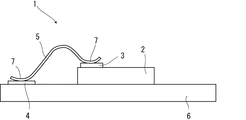
図1にパワー半導体装置1の概略部分断面図を示す。パワー半導体素子2上には金属電極が設けられ、この金属電極に金属ワイヤ5の一端を接続し、パワー半導体装置のリードフレームや基板6上の電極や、複数搭載された別のパワー半導体素子上の金属電極に当該金属ワイヤの他端を接続して回路を構成する。ここでは、対象とするパワー半導体素子2上の金属電極を「素子電極3」と呼び、素子電極3と接続するための金属電極を「接続電極4」と呼ぶこととする。
FIG. 1 is a schematic partial cross-sectional view of the
パワー半導体装置においては、電極間を接続する上記金属ワイヤとして通常は数百μm径の太径Alワイヤを用いている(特許文献1)。金属ワイヤとしてCuワイヤがLSIの一部で使用されているが、パワー半導体装置の太径ワイヤとしては用いられていない。Cuワイヤでは硬度並びに加工硬化指数が大きく、特に太線径での超音波による接続の際に素子電極を損傷する確率が高いためである。金ワイヤは、LSIのボールボンディングには多用されているが、パワー半導体装置で利用する太線径では材料費が特に高価格となるため、実用化はほとんどされていない。 In a power semiconductor device, a large-diameter Al wire having a diameter of several hundred μm is usually used as the metal wire for connecting electrodes (Patent Document 1). A Cu wire is used as a metal wire in a part of the LSI, but it is not used as a large-diameter wire of a power semiconductor device. This is because the Cu wire has high hardness and work hardening index, and in particular, has a high probability of damaging the device electrode when connected by ultrasonic waves with a thick wire diameter. Gold wires are frequently used for ball bonding of LSIs, but material costs are particularly high for thick wire diameters used in power semiconductor devices, so that they have hardly been put to practical use.
特許文献2には、Ag又はAg合金のみから構成される芯材をAuのみから構成される外皮材で被覆したボンディングワイヤが開示されている。特許文献3には、Agを有する芯材にPd、Pt、Niを有する被覆層を有するボンディングワイヤが開示されている。しかしいずれも、線径が25μmあるいは40μm以下の細径を対象としている。また、特許文献2にも記載されているように、Al電極にAgワイヤをボンディングすると、Al2Ag金属間化合物の生成が顕著であり、この金属間化合物は非常に脆いものであるから接合部の信頼性を得ることができないという問題があるため、特にパワー半導体装置にAgワイヤを用いることができなかった。特許文献4にはパワー半導体モジュールとして、電極とパッドとを接合する導体にAgを用いる例が開示されているが、導体とパッド及び電極とは半田によって接合されており、ボールボンディングやウェッジボンディングを対象とするものではない。
なお、特許文献5には、半導体集積回路装置の一部である半導体チップ上のアルミニウム系または銅系のボンディング・パッド上に、バリア・メタル膜を介して、金系表面メタル層を設け、外部との接続のための金系または銅系のボンディング・ワイヤ接合またはボンディング・ボールを設けたものが開示されている。アルミニウムと金の相互作用によるカーケンダルボイド等の接続不良を防止するためである。あくまで金ワイヤ又は銅ワイヤを対象とするものであり、また太径のワイヤを用いるパワー半導体装置を対象とするものではない。
In
パワー半導体装置を大容量化すると、内蔵するパワー半導体素子に大電流が流れることになる。半導体素子に大電流が繰り返し通電されると、半導体素子の発熱が著しく、また金属ワイヤ自身の通電加熱による発熱も無視できない。この発熱に伴い、半導体素子とそれに接続された金属ワイヤの温度が上昇と下降を繰り返すこととなる。そのため、各接合部には部材間の熱膨張率の相違に基づいて熱応力が発生し、この熱応力により電極と金属ワイヤの接合界面や界面付近でクラックを生じる可能性がある。 When the capacity of the power semiconductor device is increased, a large current flows through the built-in power semiconductor element. When a large current is repeatedly supplied to the semiconductor element, the heat generated by the semiconductor element is significant, and the heat generated by the current heating of the metal wire itself cannot be ignored. With this heat generation, the temperature of the semiconductor element and the metal wire connected to the semiconductor element repeatedly rises and falls. Therefore, a thermal stress is generated in each joint portion based on a difference in thermal expansion coefficient between members, and the thermal stress may cause a crack at or near the joint interface between the electrode and the metal wire.
また、近年注目されているSiC基板を有するパワー半導体素子を用いたパワー半導体装置においては、SiC結晶のバンドギャップがSi結晶に比べてはるかに大きいために250℃以上の高温での動作が可能とされており、高温での動作を前提としたパワー半導体装置が検討されている。このように高温での動作が前提となるパワー半導体装置では、装置の耐熱性がますます重要となっている。従来から用いられているAlワイヤは融点が660℃近傍と比較的低温であるため、高温での使用では再結晶が生じ、ワイヤ内部や接合部の界面でクラックやボイド欠陥を生じやすいという問題がある。 In addition, power semiconductor devices using a power semiconductor element having a SiC substrate that has been attracting attention in recent years can operate at a high temperature of 250 ° C. or higher because the band gap of the SiC crystal is much larger than that of the Si crystal. Power semiconductor devices that are premised on operation at high temperatures are being studied. In such a power semiconductor device that is premised on operation at a high temperature, the heat resistance of the device becomes more and more important. Conventionally used Al wire has a relatively low melting point of around 660 ° C., so recrystallization occurs when used at a high temperature, and cracks and void defects are likely to occur inside the wire and at the interface of the joint. is there.
パワー半導体装置内の接続に用いる金属ワイヤとして、従来から用いられているAlワイヤは、常温での硬度が低く素子側のAl電極への接合も超音波振動により比較的容易に接合できるという利点がある。一方、上述のようにパワー半導体装置の電流容量の大容量化、高温環境での使用に際しては、Alは融点が660℃近傍と低いので高温での耐熱性が十分ではなく、またAlは比抵抗が2.7μΩ・cmと良導体の中では最も高い部類に入り、Alワイヤに大電流を流したときのワイヤの発熱が無視できない。熱応力により、Alのストレスマイグレーションなどを生じ欠陥が発生する懸念がある。また抵抗は温度上昇にともない、さらに大となるので、高温下での使用では特に、アルミニウムの粒成長や再結晶時におこる欠陥が問題となるだけではなく、融点以上の温度となり、ワイヤの溶断につながることも懸念される。 Conventionally used Al wire as a metal wire for connection in power semiconductor devices has the advantage that it has a low hardness at room temperature and can be bonded to the Al electrode on the element side relatively easily by ultrasonic vibration. is there. On the other hand, when the current capacity of the power semiconductor device is increased as described above and Al is used in a high temperature environment, Al has a low melting point of around 660 ° C., so that the heat resistance at high temperature is not sufficient, and Al has a specific resistance. Is 2.7 μΩ · cm, which is the highest among the good conductors, and the heat generation of the wire when a large current is passed through the Al wire cannot be ignored. There is a concern that the thermal stress causes a stress migration of Al and causes defects. In addition, resistance increases further with increasing temperature, so defects especially during aluminum grain growth and recrystallization are not only problematic when used at high temperatures. There is also concern about being connected.
本発明は、パワー半導体装置の電流容量の大容量化、高温環境での使用に際し、熱応力が発生しても問題なく使用でき、ワイヤ自身の発熱を低減でき、例えば200℃以上の高温環境でも接合部の信頼性を確保することができるパワー半導体装置及びその製造方法並びにパワー半導体装置に用いるボンディングワイヤを提供することを目的とする。 The present invention can increase the current capacity of a power semiconductor device and can be used without any problem even when thermal stress occurs when used in a high temperature environment, and can reduce the heat generation of the wire itself, for example, even in a high temperature environment of 200 ° C. or higher. It is an object of the present invention to provide a power semiconductor device capable of ensuring the reliability of the joint, a manufacturing method thereof, and a bonding wire used in the power semiconductor device.
パワー半導体装置の接続に用いる金属ワイヤの材料としてAgを用いることができれば、Agの比抵抗は1.6μΩ・cmであってAlの2.7μΩ・cmよりも低く、大電流での使用時に金属ワイヤ自身の発熱を低減することができる。またAgは融点が962℃であってAlの融点660℃よりも遙かに高く、高温での耐熱性を改善することができる。AgはAlと比較して融点が高いためにストレスマイグレーションなどによる欠陥が生じにくい。またCuと比較して、変形能が高く応力を吸収できるため、熱応力によるクラックなど破壊に対する耐性も優れている。また、Cuワイヤと対比し、Agワイヤであれば常温での硬度が低く加工硬化も少ないのでワイヤボンディングの超音波印加による接合時における素子電極損傷の可能性が低い。 If Ag can be used as the material of the metal wire used for connecting the power semiconductor device, the specific resistance of Ag is 1.6 μΩ · cm, which is lower than 2.7 μΩ · cm of Al. Heat generation of the wire itself can be reduced. Ag has a melting point of 962 ° C., which is much higher than the melting point of Al, 660 ° C., and can improve heat resistance at high temperatures. Since Ag has a higher melting point than Al, defects due to stress migration are less likely to occur. In addition, compared with Cu, it has high deformability and can absorb stress, so it has excellent resistance to breakage such as cracks caused by thermal stress. Further, in contrast to the Cu wire, an Ag wire has a low hardness at normal temperature and a low work hardening, so that the possibility of element electrode damage during bonding by applying ultrasonic waves during wire bonding is low.
一方、素子電極としてAl電極を用いた場合、AgワイヤをAl電極と接合する際、Ag2Alなどの金属間化合物が界面に生成され、当該金属間化合物は非常に脆くかつ金属間化合物生成箇所にボイドが生じるため、信頼性の良好な接合が困難であった。そのため、特にパワー半導体装置に用いる直径50μm以上の太径の金属ワイヤにおいては、Agワイヤを使用することができなかった。また、太径のAgワイヤをボールボンディングによって電極に接合しようとすると、大気中では良好な球状のボールが形成できないという問題があった。On the other hand, when an Al electrode is used as the element electrode, when an Ag wire is joined to the Al electrode, an intermetallic compound such as Ag 2 Al is generated at the interface, and the intermetallic compound is very brittle and an intermetallic compound is generated. Therefore, it is difficult to bond with high reliability. For this reason, an Ag wire could not be used particularly for a thick metal wire having a diameter of 50 μm or more used for a power semiconductor device. Further, when trying to join a large-diameter Ag wire to the electrode by ball bonding, there is a problem that a good spherical ball cannot be formed in the atmosphere.
それに対し、発明者らは、素子電極に50Å厚以上のNi、Cr、Cu、Pd、V、Ti、Pt、Zn、Ag、Au、W、Alの金属のいずれか1種類の金属またはこれらを2種以上のみから構成される合金のみから構成される層を1層以上、隣り合う前記素子電極および前記層の金属成分が異なるように有する電極を用い、かつワイヤボンディングにボールボンディングではなくウェッジボンディング(ウェッジ接合)を用いることにより、金属ワイヤとしてAg又はAg合金ワイヤを用いた場合でも電極とワイヤ接合部の信頼性が確保できることを見出した。 On the other hand, the inventors used any one kind of metal of Ni, Cr, Cu, Pd, V, Ti, Pt, Zn, Ag, Au, W, and Al having a thickness of 50 mm or more for the element electrode or these. Using one or more layers composed only of an alloy composed of only two or more types, electrodes having adjacent element electrodes and metal components of the layers different from each other, and wire bonding instead of ball bonding By using (wedge bonding), it has been found that the reliability of the electrode and the wire bonding portion can be secured even when Ag or an Ag alloy wire is used as the metal wire.
本発明は、上記知見に基づいてなされたものであり、その要旨とするところは以下のとおりである。
(1)パワー半導体素子及び当該パワー半導体素子上の金属電極(以下「素子電極」という。)と当該素子電極と接続するための金属電極(以下「接続電極」という。)を有し、素子電極と接続電極とを金属ワイヤによって双方ともウェッジ接続したパワー半導体装置において、
前記素子電極をAl、Cu、NiまたはTi素子電極とし、
前記金属ワイヤは直径150μm超2mm以下のAg又はAg合金ワイヤであり、
前記Al、Cu、NiまたはTi素子電極は50Å厚以上のNi、Cr、Cu、Pd、V、Ti、Pt、Zn、Ag、Au、W、Alの金属(以下「被覆層金属」という。)のいずれか1種類の金属又は前記被覆層金属の2種類以上のみから構成される合金のみから構成される層(以下「電極被覆層」という。)の1層以上を隣り合う前記Al、Cu、NiまたはTi素子電極および電極被覆層の金属成分が異なるように有し、
前記電極被覆層の最表層がAg、AuまたはPdであり、
前記素子電極がAl素子電極で、前記電極被覆層の最表層がAgの場合には、
最表層の電極被覆層より下層に前記被覆層金属からAgを除いた金属のいずれか1種類の金属又は前記被覆層金属の2種類以上のみから構成される合金のみから構成される電極被覆層の1層以上を隣り合う前記素子電極および電極被覆層の金属成分が異なるように有することを特徴とするパワー半導体装置。
(2)前記Ag又はAg合金ワイヤの表面に30Å厚以上のPd、Au、Zn、Pt、Ni、Snの1種以上又はこれらの合金若しくはこれら金属の酸化物又は窒化物を有するワイヤ被覆層を有することを特徴とする(1)に記載のパワー半導体装置。
(3)前記Ag又はAg合金ワイヤと素子電極及び接続電極との間の接続が、超音波を利用して接続されており、接続時の電極又はワイヤのいずれかの温度が60℃以上で接続されていることを特徴とする(1)又は(2)に記載のパワー半導体装置。
(4)前記ワイヤ表面のワイヤ被覆層が、ワイヤと電極の接続を行った後に、湿式又は乾式若しくはナノ粒子金属の被着によるコーティングにより行われていることを特徴とする(2)に記載のパワー半導体装置。
(5)前記パワー半導体素子がSiC半導体を用いた素子であることを特徴とする(1)乃至(4)のいずれかに記載のパワー半導体装置。
(6)前記Ag又はAg合金ワイヤと素子電極及び接続電極との間の接続を超音波を利用して行い、接続時の電極又はワイヤのいずれかの温度を60℃以上として接続することを特徴とする(1)又は(2)に記載のパワー半導体装置の製造方法。
(7)ワイヤと電極の接続を行った後に、湿式又は乾式若しくはナノ粒子金属の被着によるコーティングにより前記ワイヤ表面の被覆層を形成することを特徴とする(2)に記載のパワー半導体装置の製造方法。
(8)直径が150μm超2mm以下である半導体接続用のAg又はAg合金ボンディングワイヤであって、表面にPd、Au、Zn、Pt、Ni、Snの1種以上又はこれらの合金若しくはこれら金属の酸化物又は窒化物を有するワイヤ被覆層を有し、前記ボンディングワイヤの残留抵抗比が5以上2000以下であり、前記ボンディングワイヤ被覆層の厚みがボンディングワイヤ直径の1/5以下でありかつ10Å以上であり、前記ボンディングワイヤ被覆層とボンディングワイヤ母材との間にワイヤ被覆層が有する金属とAgの拡散層を有し、該拡散層の厚みが50Å以上10μm以下であることを特徴とするボンディングワイヤ。
(9)前記ボンディングワイヤの残留抵抗比が80以上1000以下であることを特徴とする(8)に記載のボンディングワイヤ。
(10)前記ボンディングワイヤの破断伸びが15%以上であることを特徴とする(8)または(9)に記載のボンディングワイヤ。
(11)前記ボンディングワイヤの破断伸びが25%以上であることを特徴とする(10)に記載のボンディングワイヤ。
(12)ワイヤに被覆層を形成した後、250℃以上の温度で熱処理し、さらに、伸線したことを特徴とする(8)ないし(11)のいずれか1つに記載のボンディングワイヤ。
This invention is made | formed based on the said knowledge, The place made into the summary is as follows.
(1) A power semiconductor element, a metal electrode (hereinafter referred to as “element electrode”) on the power semiconductor element, and a metal electrode (hereinafter referred to as “connection electrode”) for connection to the element electrode, In the power semiconductor device in which both the connection electrode and the connection electrode are wedge-connected by a metal wire,
The element electrode is an Al, Cu, Ni or Ti element electrode,
The metal wire is an Ag or Ag alloy wire having a diameter of more than 150 μm and 2 mm or less,
The Al, Cu, Ni or Ti element electrode is a metal of Ni, Cr, Cu, Pd, V, Ti, Pt, Zn, Ag, Au, W, or Al (hereinafter referred to as “coating layer metal”) having a thickness of 50 mm or more. Any one of the above-described Al, Cu, and the adjacent layers of one or more layers composed of only one kind of metal or an alloy composed of only two or more kinds of the coating layer metals (hereinafter referred to as “electrode coating layer”). The metal component of the Ni or Ti element electrode and the electrode coating layer is different,
The outermost layer of the electrode coating layer is Ag, Au or Pd,
When the element electrode is an Al element electrode and the outermost layer of the electrode coating layer is Ag,
An electrode coating layer composed of only one kind of metal obtained by removing Ag from the coating layer metal or an alloy composed of only two or more kinds of the coating layer metal below the outermost electrode coating layer. A power semiconductor device having one or more layers so that the metal components of the element electrode and the electrode coating layer adjacent to each other are different.
(2) A wire coating layer having one or more of Pd, Au, Zn, Pt, Ni, Sn, an alloy thereof, or an oxide or nitride of these metals having a thickness of 30 mm or more on the surface of the Ag or Ag alloy wire. The power semiconductor device as set forth in (1), characterized by comprising:
(3) The connection between the Ag or Ag alloy wire and the element electrode and the connection electrode is connected using ultrasonic waves, and the connection is performed when the temperature of either the electrode or the wire is 60 ° C. or higher. The power semiconductor device according to (1) or (2), wherein
(4) The wire coating layer on the surface of the wire is formed by wet, dry, or coating by deposition of nanoparticle metal after connecting the wire and the electrode. Power semiconductor device.
(5) The power semiconductor device according to any one of (1) to (4), wherein the power semiconductor element is an element using a SiC semiconductor.
(6) The connection between the Ag or Ag alloy wire and the element electrode and the connection electrode is performed using ultrasonic waves, and the temperature of either the electrode or the wire at the time of connection is 60 ° C. or higher. The manufacturing method of the power semiconductor device according to (1) or (2).
(7) The power semiconductor device according to (2), wherein after the wire and the electrode are connected, a coating layer on the surface of the wire is formed by wet, dry, or coating by deposition of nanoparticle metal. Production method.
(8) Ag or Ag alloy bonding wire for semiconductor connection having a diameter of more than 150 μm and not more than 2 mm, and having one or more of Pd, Au, Zn, Pt, Ni, Sn on the surface thereof, alloys of these or these metals has a wire coating layer have a oxide or nitride, the residual resistance ratio of the bonding wire is not less 5 to 2,000, the thickness of the bonding wire coating layer is 1/5 or less of the bonding wire diameter and 10Å It is above, It has the metal and Ag diffusion layer which a wire coating layer has between the said bonding wire coating layer and a bonding wire base material, The thickness of this diffusion layer is 50 to 10 micrometer, It is characterized by the above-mentioned. Bonding wire.
(9) The bonding wire according to (8), wherein the bonding wire has a residual resistance ratio of 80 or more and 1000 or less .
(10) The bonding wire according to (8) or (9) , wherein the elongation at break of the bonding wire is 15% or more.
(11) The bonding wire according to (10), wherein the breaking elongation of the bonding wire is 25% or more .
(12) The bonding wire according to any one of (8) to (11), wherein a coating layer is formed on the wire, heat treated at a temperature of 250 ° C. or higher, and further drawn.
本発明は、パワー半導体素子及び当該パワー半導体素子上の金属電極(素子電極)と当該素子電極と接続するための金属電極(接続電極)を有し、素子電極と接続電極とを金属ワイヤによって双方ともウェッジ接続したパワー半導体装置において、金属ワイヤが直径50μm超2mm以下のAg又はAg合金ワイヤであり、素子電極は表面に50Å厚以上の被覆層金属(Ni、Cr、Cu、Pd、V、Ti、Pt、Zn、Ag、Au、W、Al)のいずれか1種類の金属又は前記被覆層金属の2種以上のみから構成される合金のみから構成される層である電極被覆層の1層以上を隣り合う前記素子電極および電極被覆層の金属成分が異なるように有することにより、Agワイヤを用いるにもかかわらず電極との接合部信頼性を確保でき、大電流での使用時に金属ワイヤ自身の発熱を低減でき、高温での耐熱性を改善することができる。 The present invention includes a power semiconductor element, a metal electrode (element electrode) on the power semiconductor element, and a metal electrode (connection electrode) for connecting to the element electrode, and the element electrode and the connection electrode are both connected by a metal wire. In both power-connected semiconductor devices, the metal wire is an Ag or Ag alloy wire having a diameter of more than 50 μm and 2 mm or less, and the element electrode has a coating layer metal (Ni, Cr, Cu, Pd, V, Ti, having a thickness of 50 mm or more on the surface. , Pt, Zn, Ag, Au, W, Al), or one or more electrode coating layers that are layers composed of only one type of metal or an alloy composed of only two or more types of the coating layer metal. Can be ensured the reliability of the junction with the electrode despite the use of the Ag wire, so that the adjacent element electrode and the electrode coating layer have different metal components. It can reduce heat generation of the metal wire itself when used in, it is possible to improve the heat resistance at high temperatures.
パワー半導体素子上の金属電極(素子電極)として、Al電極、Cu電極、Ni電極、Ti電極を用いることができ、好ましくはAl電極が用いられる。以下、まずは素子電極としてAl電極を用いる場合について説明する。 As a metal electrode (element electrode) on the power semiconductor element, an Al electrode, a Cu electrode, a Ni electrode, or a Ti electrode can be used, and an Al electrode is preferably used. Hereinafter, a case where an Al electrode is used as the element electrode will be described first.
前述のとおり、素子電極としてAl電極を用いた場合、直径50μm超の太径のAg又はAg合金ワイヤをAl電極と接合する際、Ag2Alなどの金属間化合物が界面に生成され、当該金属間化合物は非常に脆くかつ金属間化合物生成箇所にボイドが生じるため、信頼性の良好な接合が困難であった。それに対し本発明においては、素子電極の表面に50Å厚以上の被覆層金属(Ni、Cr、Cu、Pd、V、Ti、Pt、Zn、Ag、Au、W、Al)のいずれか1種類の金属又は前記被覆層金属を2種類以上のみから構成される合金のみから構成される電極被覆層の1層以上を隣り合う前記素子電極および電極被覆層の金属成分が異なるように有する電極を用い、かつワイヤボンディングにウェッジ接合を用いることにより、金属ワイヤとして直径50μm超の太径のAg又はAg合金ワイヤを用いた場合でも電極とワイヤ接合部の信頼性が確保できることを見出した。As described above, when an Al electrode is used as the element electrode, an intermetallic compound such as Ag 2 Al is generated at the interface when a large Ag or Ag alloy wire having a diameter of more than 50 μm is joined to the Al electrode, and the metal Since the intermetallic compound is very brittle and voids are generated at the site where the intermetallic compound is produced, it is difficult to bond with good reliability. On the other hand, in the present invention, the surface of the device electrode has a coating layer metal (Ni, Cr, Cu, Pd, V, Ti, Pt, Zn, Ag, Au, W, Al) having a thickness of 50 mm or more. Using an electrode having one or more electrode coating layers composed of only metal or an alloy composed of only two or more types of the coating layer metal so that the metal components of the adjacent element electrode and electrode coating layer are different, Further, it has been found that by using wedge bonding for wire bonding, the reliability of the electrode and wire bonding portion can be ensured even when a large diameter Ag or Ag alloy wire having a diameter of more than 50 μm is used as the metal wire.
なお1層以上の電極被覆層を隣り合う素子電極および電極被覆層の金属成分が異なるように有するとあることから、電極被覆層を素子電極の表面に1層以上形成するにあたり、隣り合う素子電極ないし電極被覆層を構成する金属あるいは合金の金属成分は相違するものであり、Al電極、Cu電極、Ni電極、Ti電極の上に、それぞれ、Al、Cu、Ni、Tiの電極被覆層を構成したりすることや、同種の被覆層金属あるいはその合金のみから構成される電極被覆層を重ねて構成することは除かれる。 Since there are one or more electrode coating layers having different metal components in the adjacent element electrode and electrode coating layer, adjacent element electrodes are formed when forming one or more electrode coating layers on the surface of the element electrode. The metal components of the metal or alloy constituting the electrode coating layer are different, and the electrode coating layers of Al, Cu, Ni and Ti are formed on the Al electrode, Cu electrode, Ni electrode and Ti electrode, respectively. Or an electrode covering layer composed of only the same kind of covering layer metal or its alloy is excluded.
Al電極表面に被覆層金属または被覆層金属の合金のみから構成される電極被覆層を形成することにより、Agワイヤをウェッジ接合した際、これらの金属はAl電極とは異なり、AlとAgの接合部に形成されるボイドなどの欠陥の多い金属間化合物の形成を抑制することができる。またこれらの金属とAgとは超音波接合により、比較的良好な接合部に拡散層を形成することができる。これらの金属の表面が酸化により接合性が阻害される場合には、酸化防止のために表面をPd,Au、Agなどの貴金属などで被覆しておくことも効果的である。特にV,Ti,Cr,NiはAl電極との密着性に効果があり、さらにAgとAlとの拡散のバリアとしても有効に機能する。またCu,Pd,Pt,ZnはAgとの初期接合性を改善するのに好適である。それらの金属を複数層重ねることも、初期接合性と長期の接合信頼性を確保するために有効である。 By forming an electrode coating layer composed only of a coating layer metal or a coating layer metal alloy on the surface of the Al electrode, when the Ag wire is wedge-bonded, these metals are different from the Al electrode and are bonded to Al and Ag. The formation of intermetallic compounds with many defects such as voids formed in the portion can be suppressed. Further, these metals and Ag can form a diffusion layer at a relatively good joint by ultrasonic bonding. When the surface of these metals is obstructed by oxidation, it is also effective to cover the surface with a noble metal such as Pd, Au, Ag, etc. to prevent oxidation. In particular, V, Ti, Cr, and Ni are effective in adhesion to the Al electrode, and also function effectively as a diffusion barrier between Ag and Al. Cu, Pd, Pt, and Zn are suitable for improving initial bondability with Ag. It is also effective to stack a plurality of layers of these metals in order to ensure initial bondability and long-term bond reliability.
また、電極被覆層の厚さが50Å以上であれば、上記効果を発揮することができる。50Å未満では、電極被覆層に欠陥が生じやすいからである。したがって、複数の電極被覆層を積層する場合、それぞれの電極被覆層厚さを50Å以上とする。電極被覆層の厚さが100Å以上であればより好ましい。200Å以上であればさらに好ましい。 Moreover, the said effect can be exhibited if the thickness of an electrode coating layer is 50 mm or more. This is because if it is less than 50 mm, defects are likely to occur in the electrode coating layer. Therefore, when laminating a plurality of electrode coating layers, the thickness of each electrode coating layer is 50 mm or more. More preferably, the thickness of the electrode coating layer is 100 mm or more. More preferably, it is 200 mm or more.
電極被覆層の厚さの上限は5μmとすると好ましい。5μm超では、コスト高になる上、接合条件により、接合部の電気抵抗値にばらつきを与える要因となるからである。 The upper limit of the thickness of the electrode coating layer is preferably 5 μm. This is because if it exceeds 5 μm, the cost becomes high and the electric resistance value of the joint portion varies depending on the joining condition.
Al電極に最表層の電極被覆層を構成する被覆層金属としてAgあるいはAuのみから構成される電極被覆層を用いる場合には、Al電極に直接AgあるいはAuのみから構成される電極被覆層を設けるのではなく、Al電極とAgあるいはAuのみから構成される電極被覆層の間に中間層として、被覆層金属からAg除いたNi、Cr、Cu、Pd、V、Ti、Pt、Zn、Au、W、Alのいづれか1種類の金属又は被覆層金属の2種類以上の金属のみから構成される合金のみから構成される電極被覆層の1層以上を隣り合う前記素子電極および電極被覆層の金属成分が異なるように有することとすると好ましい。 When an electrode coating layer composed only of Ag or Au is used as the coating layer metal constituting the outermost electrode coating layer on the Al electrode, an electrode coating layer composed only of Ag or Au is directly provided on the Al electrode. Instead of Ni, Cr, Cu, Pd, V, Ti, Pt, Zn, Au, which is an intermediate layer between the Al electrode and the electrode coating layer composed only of Ag or Au, excluding Ag from the coating layer metal. Metal component of the element electrode and the electrode coating layer adjacent to one or more of the electrode coating layer composed of only an alloy composed of only one kind of metal of W or Al or two or more kinds of metals of the coating layer metal Are preferably different from each other.
これら中間層に用いる金属は密着性と拡散バリア性を有するため、昇温時の反応によって生成する化合物が起因となって形成されるボイドの問題を回避することが可能になる。例えば、Al電極の上にCr被覆層、Ni被覆層、最表面にAg被覆層をこの順序で形成する場合(「Al/Cr/Ni/Ag」と表示する。)を例にとると、Cr被覆層はAl電極表面との密着性を向上する効果を有し、Ni被覆層は拡散を防止してAlとAgの化合物形成を阻止する作用を有し、最表面のAg被覆層はNi被覆層の表面酸化を防止する機能を有している。同様に、Al/Ti/Pd/Ag、Al/Ni/Ag、Al/TiW/Ag、Al/NiV/Ag、Al/NiV/Cu/Ag、Al/Ni/Cu/Ag、Al/Cr/Ni/Cu/Ag、Al/Zn/Pd/Ni/Agなど密着性と拡散バリア性を有する金属の組み合わせが好適である。これらの中間層に用いられる膜の構造は、最表面層がAgである場合に限らず、Al電極と最表面金属との中間の層として用いられることにより、Agワイヤとの接合の信頼性を高めるために有効である。 Since the metal used for these intermediate layers has adhesion and diffusion barrier properties, it is possible to avoid the problem of voids that are formed due to the compounds generated by the reaction during temperature rise. For example, when the Cr coating layer, the Ni coating layer, and the Ag coating layer on the outermost surface are formed in this order (displayed as “Al / Cr / Ni / Ag”), Cr is taken as an example. The coating layer has the effect of improving the adhesion with the surface of the Al electrode, the Ni coating layer has the function of preventing diffusion and blocking the formation of Al and Ag compounds, and the outermost Ag coating layer is coated with Ni. It has a function of preventing surface oxidation of the layer. Similarly, Al / Ti / Pd / Ag, Al / Ni / Ag, Al / TiW / Ag, Al / NiV / Ag, Al / NiV / Cu / Ag, Al / Ni / Cu / Ag, Al / Cr / Ni A combination of metals having adhesion and diffusion barrier properties such as / Cu / Ag and Al / Zn / Pd / Ni / Ag is preferable. The structure of the film used for these intermediate layers is not limited to the case where the outermost surface layer is Ag, but is used as an intermediate layer between the Al electrode and the outermost surface metal, thereby improving the reliability of bonding with the Ag wire. Effective to enhance.
また、電極被覆層の最表層にAg、Au、Pdを用いることにより、その下の中間層の金属の酸化を防止できるという効果を有する。また、最表層がAgであっても、その下の中間層に被覆層金属からAgを除いた金属又は被覆層金属2種類以上の金属のみから構成される合金のみから構成される電極被覆層を有することにより、Ag層とAl電極による金属間化合物形成を防止することができる。電極がAl電極以外の金属電極の場合には、電極被覆層をAg単独層としても良い。 Further, the use of Ag, Au, or Pd as the outermost surface layer of the electrode coating layer has an effect of preventing the oxidation of the metal in the intermediate layer therebelow. Moreover, even if the outermost layer is Ag, an electrode coating layer composed only of a metal obtained by removing Ag from the coating layer metal or an alloy composed of only two or more types of coating layer metals is provided in the intermediate layer below it. By having it, formation of intermetallic compounds by the Ag layer and the Al electrode can be prevented. When the electrode is a metal electrode other than the Al electrode, the electrode coating layer may be an Ag single layer.
半導体素子のワイヤ接合用電極にCu電極を用いることは従来検討されてこなかったが、ウエッジ用ワイヤにAgを主成分とするワイヤを用いることを目的として、半導体素子の電極にCuを用いることは好適である。Agワイヤは、Cuワイヤに比較すると格段に接合時のチップ損傷を軽減できるが、従来のAlワイヤに比較すると硬度は高い。したがって、Agワイヤの接合部に硬度の低い従来のAl電極に代えてCu電極を採用することで、チップ損傷の確率を低減する効果が発現する。特に電極被覆層を3μm以上の膜厚とすることで、さらにその効果を高めることができる。またAgワイヤと接合された場合には、CuとAgの相互拡散層が0.1μm以上形成されていることが好適である。 The use of a Cu electrode as a wire bonding electrode of a semiconductor element has not been studied in the past, but the use of Cu as an electrode of a semiconductor element for the purpose of using a wire mainly composed of Ag as a wedge wire. Is preferred. The Ag wire can remarkably reduce chip damage at the time of bonding as compared with the Cu wire, but the hardness is higher than that of the conventional Al wire. Therefore, by adopting a Cu electrode in place of a conventional Al electrode having a low hardness at the joint portion of the Ag wire, an effect of reducing the probability of chip damage appears. In particular, when the electrode coating layer has a thickness of 3 μm or more, the effect can be further enhanced. In addition, when bonded to an Ag wire, it is preferable that a mutual diffusion layer of Cu and Ag is formed to have a thickness of 0.1 μm or more.
素子電極としてCu電極を用いた場合、電極被覆層として、酸化防止の目的でAu、Pd、Niの金属層又はこれらの合金層を1層以上有することとすると、接合性向上のために有効であり、望ましい。 When a Cu electrode is used as the element electrode, it is effective for improving the bonding property if the electrode covering layer has at least one metal layer of Au, Pd, Ni or an alloy layer thereof for the purpose of preventing oxidation. Yes, desirable.
素子電極として、電極表面の下層に、表面の電極材料とは異なる金属が配置されていても良い。例えばAl電極において、電極表面にAl層を有し、下層にAlとは異なる金属、例えばCuを有する層が形成されていても良い。半導体素子の内部配線に用いられる金属がCuである場合、素子電極がAl電極であれば、電極表面にAl層を有し、下層に半導体素子の内部配線と同じCuの層を形成することとなる。Cu電極において、電極表面にCu層を有し、下層に半導体素子の内部配線と同じAl層を形成しても良い。 As the element electrode, a metal different from the electrode material on the surface may be disposed below the electrode surface. For example, in an Al electrode, a layer having an Al layer on the electrode surface and a metal different from Al, for example, Cu may be formed in the lower layer. When the metal used for the internal wiring of the semiconductor element is Cu, if the element electrode is an Al electrode, an Al layer is formed on the electrode surface, and the same Cu layer as the internal wiring of the semiconductor element is formed in the lower layer. Become. In the Cu electrode, a Cu layer may be provided on the electrode surface, and the same Al layer as the internal wiring of the semiconductor element may be formed in the lower layer.
本発明においてAgワイヤとは、Ag含有量が99質量%以上のAgを用いたワイヤをいう。また、Ag合金ワイヤとは、Ag含有量が50質量%以上のAg合金を用いたワイヤをいう。特にAuやPdまたはその両方を加えたAg合金が特に有効である。Agは硫化しやすいという問題があり、これを抑制するためAuとの合金が有効である。また前述の通りAgはAlとの接合によってAg2Alのような金属間化合物を生成するという問題があるが、この抑制にはAgとPdとの合金が有効である。Auは1質量%以上10質量%以下が望ましく、Pdは0.1質量%以上5質量%以下が望ましい。In the present invention, the Ag wire refers to a wire using Ag with an Ag content of 99% by mass or more. Moreover, an Ag alloy wire means the wire using Ag alloy whose Ag content is 50 mass% or more. In particular, an Ag alloy added with Au, Pd, or both is particularly effective. Ag has a problem that it is easily sulfided, and an alloy with Au is effective for suppressing this. Further, as described above, Ag has a problem that an intermetallic compound such as Ag 2 Al is formed by bonding with Al, and an alloy of Ag and Pd is effective for this suppression. Au is desirably 1% by mass or more and 10% by mass or less, and Pd is desirably 0.1% by mass or more and 5% by mass or less.
本発明が対象とするAg又はAg合金ワイヤは直径が50μm超2mm以下のものを対象とする。ワイヤ直径50μm超において、本発明の効果が特に顕著に発揮されるからである。ワイヤ直径150μm以上であるとより好ましい。ワイヤ直径200μm以上であるとさらに好ましい。ただし、ワイヤ直径が2mmを超えると、接合時に必要な変形を得るための超音波出力が過大となり、チップへのダメージが懸念されるので、ワイヤ直径上限を2mmとした。 The Ag or Ag alloy wire targeted by the present invention is intended for those having a diameter of more than 50 μm and 2 mm or less. This is because the effect of the present invention is particularly remarkable when the wire diameter exceeds 50 μm. More preferably, the wire diameter is 150 μm or more. More preferably, the wire diameter is 200 μm or more. However, if the wire diameter exceeds 2 mm, the ultrasonic output for obtaining the necessary deformation at the time of joining becomes excessive, and there is a concern about damage to the chip. Therefore, the upper limit of the wire diameter is set to 2 mm.
本発明において、素子電極と接続電極(以下、2つをあわせて「電極」という。)を金属ワイヤによって双方ともウェッジ接続する。ワイヤボンディングにボールボンディングではなくウェッジボンディング(ウェッジ接合)を用いることによりはじめて、金属ワイヤとしてAg又はAg合金ワイヤを用いた場合でも電極とワイヤ接合部の信頼性が確保できる。Agワイヤにボールを形成する場合、Agワイヤの溶融、凝固時に酸化物が形成され、電極がAl以外の場合であっても、溶融、凝固時に形成される酸化物は特に接合部の信頼性を阻害する要因となる。またワイヤに大容量の電流を流すには太線径のものを使用するが、ボールを安定的に形成するには、100μm以上では困難である。細径のものを多数本接合することは、設計上不利となる上、上記理由により、信頼性を確保することも問題となる。 In the present invention, the element electrode and the connection electrode (hereinafter, the two are collectively referred to as “electrode”) are both wedge-connected by a metal wire. The use of wedge bonding (wedge bonding) instead of ball bonding for wire bonding can ensure the reliability of the electrode and the wire bonding portion even when Ag or Ag alloy wire is used as the metal wire. When forming a ball on an Ag wire, an oxide is formed when the Ag wire is melted and solidified, and even when the electrode is other than Al, the oxide formed during the melting and solidification particularly improves the reliability of the joint. It becomes a factor to inhibit. In addition, a thick wire having a large diameter is used to pass a large current through the wire, but it is difficult to form a ball stably at 100 μm or more. Joining a large number of small diameters is disadvantageous in terms of design, and ensuring reliability is also a problem for the above reasons.
電極表面の電極被覆層は、上記のように素子電極表面に形成することで有利な効果を奏するとともに、パワー半導体装置のリードフレーム上の電極や、複数搭載された別のパワー半導体素子上の金属電極など、当該素子電極と接続するための接続電極の表面に形成することによっても同様の効果を奏することができる。 The electrode coating layer on the electrode surface has an advantageous effect when formed on the surface of the element electrode as described above. The electrode on the lead frame of the power semiconductor device or a metal on another mounted power semiconductor element The same effect can be obtained by forming the electrode on the surface of the connection electrode for connecting to the element electrode.
本発明のパワー半導体装置において、Ag又はAg合金ワイヤの表面に30Å厚以上のPd、Au、Zn、Pt、Ni、Snの1種以上又はこれらの合金若しくはこれら金属の酸化物又は窒化物を少なくとも有するワイヤ被覆層を有すると好ましい。このようなワイヤ被覆層を有することにより、樹脂封止されたあとのワイヤの硫化や腐食などの反応ならびに、Agイオンとして溶出するマイグレーションを防止するとともに、ガス分子などの拡散を防止する上で効果がある。このような効果を奏するためには、ワイヤ被覆層の厚さを50Å以上とすると好ましい。また、ワイヤを半導体装置に接続する前段階においても、ワイヤ表面に上記被覆層を有していると、接合前のAgワイヤの表面酸化防止に有効である。この目的のためには、ワイヤ被覆層の厚さを50Å以上10μm以下とすると好ましい。50Å以上で表面酸化防止効果を発揮し、10μm以下とすることでワイヤ接続時の接続部の電気抵抗の安定性を確保することができる。 In the power semiconductor device of the present invention, at least one or more of Pd, Au, Zn, Pt, Ni, Sn having a thickness of 30 mm or more or an alloy or an oxide or nitride of these metals is formed on the surface of the Ag or Ag alloy wire. It is preferable to have a wire coating layer. By having such a wire covering layer, it is effective in preventing reactions such as sulfidation and corrosion of the wire after resin sealing and migration that elutes as Ag ions and also prevents diffusion of gas molecules and the like. There is. In order to exhibit such an effect, it is preferable that the thickness of the wire coating layer is 50 mm or more. Also, even before the wire is connected to the semiconductor device, having the coating layer on the wire surface is effective in preventing the surface oxidation of the Ag wire before bonding. For this purpose, it is preferable that the thickness of the wire coating layer be 50 to 10 μm. The surface oxidation-preventing effect is exhibited when the thickness is 50 mm or more, and the stability of the electrical resistance of the connection portion at the time of wire connection can be ensured when the thickness is 10 μm or less.
本発明のパワー半導体装置において、Ag又はAg合金ワイヤと素子電極及び接続電極との間の接続が、超音波を利用して接続されており、接続時の電極又はワイヤのいずれかの温度が60℃以上で接続されていると好ましい。詳細については後述する本発明の製造方法において説明する。 In the power semiconductor device of the present invention, the connection between the Ag or Ag alloy wire and the element electrode and the connection electrode is connected using ultrasonic waves, and the temperature of either the electrode or the wire at the time of connection is 60. It is preferable that the connection is performed at a temperature of ° C or higher. Details will be described later in the manufacturing method of the present invention.
本発明のパワー半導体装置においてワイヤ表面にワイヤ被覆層を形成する場合、接続前の段階で被覆層を形成しても良く、あるいは接続前には被覆層を形成せず、接続後に被覆層を形成しても良く、さらには接続前にワイヤ表面に薄い被覆層を形成し、接続後に追加でワイヤ表面に被覆を行うこととしても良い。接続後にワイヤ表面に被覆を行う場合、ワイヤと電極の接続を行った後に、湿式又は乾式若しくはナノ粒子金属の被着によるコーティングにより行うことができる。 When a wire coating layer is formed on the wire surface in the power semiconductor device of the present invention, the coating layer may be formed before the connection, or the coating layer is not formed before the connection and the coating layer is formed after the connection. Alternatively, a thin coating layer may be formed on the wire surface before connection, and the wire surface may be additionally coated after connection. In the case where the wire surface is coated after the connection, the wire and the electrode can be connected and then wet, dry, or coating by nanoparticle metal deposition.
本発明のパワー半導体装置において、パワー半導体素子がSiC半導体を用いた素子であると好ましい。SiC半導体を用いた素子は250℃以上の高温でも作動可能であるため、高温での使用を前提としたパワー半導体装置とすることができ、本発明の特徴が特に顕著に実現するからである。 In the power semiconductor device of the present invention, the power semiconductor element is preferably an element using a SiC semiconductor. This is because an element using a SiC semiconductor can operate even at a high temperature of 250 ° C. or higher, so that it can be a power semiconductor device premised on use at a high temperature, and the features of the present invention are realized particularly remarkably.
次に、本発明のパワー半導体装置の製造方法について説明する。 Next, the manufacturing method of the power semiconductor device of this invention is demonstrated.
素子電極表面に形成する電極被覆層については、めっき法、蒸着法、スパッタリング法のいずれかにより被着することができる。 The electrode coating layer formed on the element electrode surface can be applied by any one of a plating method, a vapor deposition method, and a sputtering method.
Ag又はAg合金ワイヤと素子電極及び接続電極との間の接続を超音波を利用して行い、接続時の電極又はワイヤのいずれかの温度を60℃以上として接続すると好ましい。超音波を利用することにより、ワイヤの表面を塑性変形して、新生面を露出させ、より均一な金属接合をおこなうことができる。接合時の温度を60℃以上に上昇させておくことで、超音波接合時の金属の拡散をより促進し、接合部の安定性を確保できる。120℃以上での接合はより好ましい。しかし、200℃以上では、被接合体や接合ツールなどの酸化や熱膨張差などにより、安定した接合が困難となる。 It is preferable that the connection between the Ag or Ag alloy wire, the element electrode and the connection electrode is performed using ultrasonic waves, and the temperature of either the electrode or the wire at the time of connection is 60 ° C. or higher. By using ultrasonic waves, the surface of the wire can be plastically deformed to expose the new surface, and more uniform metal bonding can be performed. By raising the temperature at the time of bonding to 60 ° C. or more, the diffusion of metal at the time of ultrasonic bonding can be further promoted, and the stability of the bonded portion can be ensured. Bonding at 120 ° C. or higher is more preferable. However, at 200 ° C. or higher, stable bonding becomes difficult due to oxidation of the objects to be bonded, bonding tools, and the like, and thermal expansion differences.
ワイヤと電極の接続を行った後に、湿式又は乾式若しくはナノ粒子金属の被着によるコーティングによりワイヤ表面のワイヤ被覆層を形成すると好ましい。ワイヤ接合後の被覆は、湿式法では、電気メッキによるもの、無電解メッキによるもの、メッキ前駆体溶液を静電塗装などによりワイヤ表面に塗布後加熱するものなどが採用できる。電気メッキあるいは無電解メッキでは、メッキ溶液中への浸漬によるものの他、電気メッキでは、電圧を印加できる筆の先端にメッキ液を供給し、ワイヤのみにメッキ液を塗布する工程により、選択的にメッキする方法も採用できる。乾式の被覆では、蒸発やスパッタなどのドライコーティングをおこなうことができる。湿式あるいは乾式のいずれにおいても、選択的な被覆方法としては、被覆不要な部分をレジストコーティングするか、あるいは全体をレジストコーティングしたのち、金属被覆が必要な部分のみレジストを選択的に剥離して被覆をおこなうことも有効である。ナノ粒子金属の被着によるコーティングについては、静電塗装の原理を応用した選択的なコーティングも可能である。 After connecting the wire and the electrode, it is preferable to form a wire coating layer on the surface of the wire by coating by wet, dry or nanoparticle metal deposition. As the coating after wire bonding, a wet method may be applied by electroplating, electroless plating, or a method in which a plating precursor solution is applied to the wire surface by electrostatic coating or the like and then heated. In electroplating or electroless plating, in addition to immersing in a plating solution, in electroplating, a plating solution is supplied to the tip of a brush to which a voltage can be applied, and the plating solution is selectively applied only to the wire. A plating method can also be adopted. With dry coating, dry coating such as evaporation or sputtering can be performed. In both wet and dry methods, the selective coating method is to either coat the part that does not require coating with resist or coat the entire part with resist coating, and then selectively strip the resist only on the part that requires metal coating. It is also effective to perform. For coating by nanoparticle metal deposition, selective coating applying the principle of electrostatic painting is also possible.
接続前のワイヤ段階でワイヤ表面に被覆層を有し、ワイヤと電極の接続を行った後にさらに上記方法でワイヤ表面に被覆を行うとより好ましい。接続前のワイヤ被覆層の厚さを50Å以上100Å以下とすることにより、接続前の表面酸化防止効果を発揮すると同時にワイヤ接続時の接続性を確保することができる。そしてワイヤ接続後の追加被覆によってワイヤ被覆層の厚さを500Å以上とすることにより、樹脂封止されたあとのワイヤ腐食などの反応を防止するとともに、ガス分子などの拡散を防止する上で効果がある。 It is more preferable to have a coating layer on the wire surface at the wire stage before connection, and further to coat the wire surface by the above method after connecting the wire and the electrode. By setting the thickness of the wire coating layer before connection to 50 mm or more and 100 mm or less, the surface oxidation prevention effect before connection can be exhibited, and at the same time, the connectivity during wire connection can be ensured. And by making the thickness of the wire coating layer 500 mm or more by additional coating after wire connection, it is effective in preventing reaction such as wire corrosion after resin sealing and also preventing diffusion of gas molecules etc. There is.
次に、本発明のパワー半導体装置に用いることのできるボンディングワイヤについて説明する。 Next, a bonding wire that can be used in the power semiconductor device of the present invention will be described.
本発明のボンディングワイヤは、直径が50μm超2mm以下である半導体接続用のAg又はAg合金ボンディングワイヤであって、表面にPd、Au、Zn、Pt、Ni、Snの1種以上又はこれらの合金若しくはこれら金属の酸化物又は窒化物を有するワイヤ被覆層を有すると好ましい。直径を上記範囲とする理由、Ag又はAg合金ボンディングワイヤとする理由、表面被覆層を規定する理由は、いずれも前述のとおりである。 The bonding wire of the present invention is an Ag or Ag alloy bonding wire for connecting a semiconductor having a diameter of more than 50 μm and 2 mm or less, and has one or more of Pd, Au, Zn, Pt, Ni, Sn on the surface or an alloy thereof. Alternatively, it is preferable to have a wire coating layer containing an oxide or nitride of these metals. The reason why the diameter is within the above range, the reason why the Ag or Ag alloy bonding wire is used, and the reason why the surface coating layer is defined are all as described above.
本発明のボンディングワイヤはさらに、ワイヤ被覆層の厚みがワイヤ直径の1/5以下でありかつ10Å以上とすると好ましく、ワイヤ直径の1/10以下でありかつ50Å以上とするとより好ましく、更に好ましくはワイヤ直径の1/20以下でありかつ100Å以上である。ワイヤ被覆層の厚みが厚くなると電気抵抗率の上昇に加え、接合時のチップへの損傷、接合性の低下が問題となる可能性が高まり、一方、被覆層の厚みが薄くなると、被覆層に欠陥を生じる場合が多くなり十分な効果を発揮できない。チップ損傷に対しては、SiC半導体では、結晶の強度が高く損傷の可能性は低くなる。またSiの場合においては、電極表面にたとえば、Ni無電解メッキ層を3μm以上積層することにより、損傷の可能性を低減することができる。 In the bonding wire of the present invention, the thickness of the wire covering layer is preferably 1/5 or less of the wire diameter and 10 mm or more, more preferably 1/10 or less of the wire diameter and 50 mm or more, and still more preferably. The wire diameter is 1/20 or less and 100 mm or more. Increasing the thickness of the wire coating layer increases the electrical resistivity, and also increases the possibility of damage to the chip during bonding and a decrease in bondability.On the other hand, if the thickness of the coating layer decreases, Defects often occur and sufficient effects cannot be exhibited. With respect to chip damage, the SiC semiconductor has a high crystal strength and a low possibility of damage. In the case of Si, the possibility of damage can be reduced by laminating, for example, a 3 μm or more Ni electroless plating layer on the electrode surface.
本発明のボンディングワイヤは、ワイヤ被覆層とワイヤ母材との間にワイヤ被覆層が有する金属とAgの拡散層を有し、該拡散層の厚みが50Å以上10μm以下であると好ましい。ワイヤ被覆層とワイヤ母材Agとの合金が行われることにより、密着性が優れ接合時に剥離が生じにくい。拡散層厚みが50Å未満ではその効果は十分ではなく、10μm超では電気抵抗の上昇への寄与が大きくなり好ましくない。該拡散層の厚みは、より好ましくは100Å以上5μm以下であり、さらに好ましくは100Å以上2μm以下である。 The bonding wire of the present invention preferably has a diffusion layer of Ag and a metal included in the wire coating layer between the wire coating layer and the wire base material, and the thickness of the diffusion layer is preferably 50 mm or more and 10 μm or less. By performing the alloy of the wire coating layer and the wire base material Ag, the adhesiveness is excellent, and peeling does not easily occur during bonding. If the thickness of the diffusion layer is less than 50 mm, the effect is not sufficient, and if it exceeds 10 μm, the contribution to the increase in electrical resistance is increased, which is not preferable. The thickness of the diffusion layer is more preferably from 100 to 5 μm, still more preferably from 100 to 2 μm.
ワイヤの残留抵抗比(RRR)とは温度293Kにおける比抵抗を4.2Kにおける比抵抗で除した値である。極低温では、熱振動による抵抗が限りなく小さくなるために、格子欠陥や不純物による抵抗が抵抗値として寄与することになるため、常温と極低温での比を求めることで、欠陥(格子欠陥や不純物)の量に依存した値が求められることになる。 The residual resistance ratio (RRR) of the wire is a value obtained by dividing the specific resistance at a temperature of 293K by the specific resistance at 4.2K. At extremely low temperatures, resistance due to thermal vibration becomes extremely small, and resistance due to lattice defects and impurities contributes as resistance. Therefore, by determining the ratio between room temperature and cryogenic temperature, defects (lattice defects and A value depending on the amount of impurities) is obtained.
例えば、ワイヤの残留抵抗比(RRR)は、常温(20℃)におけるワイヤの比抵抗を液体ヘリウム温度(4.2K)におけるワイヤの比抵抗で除することで求められる。 For example, the residual resistance ratio (RRR) of the wire can be obtained by dividing the specific resistance of the wire at normal temperature (20 ° C.) by the specific resistance of the wire at the liquid helium temperature (4.2 K).
本発明のボンディングワイヤは、ワイヤの残留抵抗比(RRR)が5以上2000以下であると好ましい。Agワイヤへの合金化により、抵抗値があがることになるが、残留抵抗比が高いほど高純度であることに対応する。特に高電流に対応する太い線径のボンディングワイヤの純度の規定は、残留抵抗比で規定することが好ましく、残留抵抗比5未満のものでは、抵抗による発熱が大となる。ワイヤの残留抵抗比(RRR)は、好ましくは80以上1000以下であり、さらに好ましくは、800以上1000以下である。 The bonding wire of the present invention preferably has a wire residual resistance ratio (RRR) of 5 or more and 2000 or less. Although the resistance value increases by alloying with the Ag wire, the higher the residual resistance ratio, the higher the purity. In particular, the purity of a bonding wire having a large wire diameter corresponding to a high current is preferably defined by the residual resistance ratio. If the bonding resistance is less than 5, the heat generated by the resistance becomes large. The residual resistance ratio (RRR) of the wire is preferably 80 or more and 1000 or less, and more preferably 800 or more and 1000 or less.
ワイヤの破断伸びとはワイヤを破断点まで伸ばした場合のワイヤの伸びΔLと伸ばす前のワイヤ長さLとから、△L/L×100(%)として得られる値であり、ワイヤの伸び△Lは引張試験機により計測することができる。 The breaking elongation of the wire is a value obtained as ΔL / L × 100 (%) from the wire elongation ΔL when the wire is stretched to the breaking point and the wire length L before being stretched, and the wire elongation Δ L can be measured by a tensile tester.
本発明のボンディングワイヤは、ワイヤの破断伸びが15%以上であると好ましい。破断伸びが大きいことは、ワイヤの変形能と関連しており、15%未満になると、超音波接合したときのチップへのダメージの可能性が大となる。ワイヤの破断伸びは、より好ましくは、20%以上、さらに好ましくは25%以上である。
本発明のボンディングワイヤの製造方法について説明する。The bonding wire of the present invention preferably has a breaking elongation of 15% or more. The fact that the elongation at break is large is related to the deformability of the wire, and if it is less than 15%, the possibility of damage to the chip when ultrasonic bonding is increased. The breaking elongation of the wire is more preferably 20% or more, and further preferably 25% or more.
The manufacturing method of the bonding wire of this invention is demonstrated.
ワイヤへの被覆方法としては、メッキ法あるいは蒸着法、スパッタリング法により被着することができる。ワイヤの製造方法は、最終線径の2倍から100倍の径で表面に金属被覆をおこなってから伸線してもよいが、最終線径で被覆をおこなってもよい。被覆の後に、加熱により拡散処理をおこなうことが好ましい。 As a method of covering the wire, it can be applied by plating, vapor deposition, or sputtering. In the method of manufacturing the wire, the surface may be coated with a metal having a diameter of 2 to 100 times the final wire diameter, and then the wire may be drawn. However, the wire may be coated with the final wire diameter. After the coating, it is preferable to carry out a diffusion treatment by heating.
電極表面の電極被覆層、ワイヤ表面のワイヤ被覆層について、厚み測定方法を説明する。被覆層の実質的な厚みとは、最表面の被覆成分濃度が内部方向に減少し、濃度が半減したところまでの厚みを被覆層の実質的な厚みとする。ワイヤ表面のワイヤ被覆層の厚みは、AES(Auger Electron Spectroscope)等によって計測することができる。表面被覆層の濃度測定は、表面からオージェ電子分光装置内で成分分析を行い、深さ方向の成分分析から決定することができる。あるいは、被覆層が比較的厚い場合には、断面研磨したのちに、表面から内部方向への分析をオージェ分光分析あるいは、EDX、EPMAなどのライン分析を行うことで、濃度測定が可能である。 A method for measuring the thickness of the electrode coating layer on the electrode surface and the wire coating layer on the wire surface will be described. The substantial thickness of the coating layer is defined as the thickness up to the point where the concentration of the coating component on the outermost surface decreases in the inner direction and the concentration is halved. The thickness of the wire coating layer on the wire surface can be measured by an AES (Auger Electron Spectroscope) or the like. The concentration measurement of the surface coating layer can be determined from the component analysis in the depth direction by performing component analysis in the Auger electron spectrometer from the surface. Alternatively, when the coating layer is relatively thick, the concentration can be measured by performing the Auger spectroscopic analysis or the line analysis such as EDX or EPMA for the analysis from the surface to the inner direction after the cross section polishing.
図1に示すようなパワー半導体装置を製造した。10mm角半導体素子2上に素子電極3として2μm厚の金属電極を形成し、チップサンプルを作成する。基板6は50mm角のCu基板に4μmのAgメッキを行う。半導体素子2としてSi、SiC素子を用い、金属電極としてAl電極、Cu電極、Ni電極、Ti電極を用いる。半導体素子2をこの基板6にダイボンディングを行う。表1に製造条件を示す。本発明例については、素子電極3の表面に表1に示す電極被覆層を1〜4層にわたって形成する。第1層が電極側の最下層であり、その上に表1に示すように第2〜第4層を形成する。被覆層の金属種類と厚さを表1に示す。
A power semiconductor device as shown in FIG. 1 was manufactured. A 2 μm-thick metal electrode is formed on the 10 mm
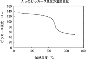
金属ワイヤ5として200μm径のAgワイヤを用い、ワイヤの種類とRRR(ワイヤの残留抵抗比)については表1に示すとおりである。2mmφのワイヤ素材に2〜10μmの金属をメッキしてワイヤ被覆層を形成する。ワイヤ被覆層がAuの場合、メッキシアン化金メッキ浴中にワイヤを連続的に繰り出し巻き取りながらメッキを行う。メッキ後250℃で熱処理の後に伸線を行う。熱処理によりワイヤ被覆層のAuの硬度は図2に示すように減少する。さらに200μmφに伸線後、再度200℃での熱処理を行い、接合実験に供する。
A 200 μm diameter Ag wire is used as the
接合には市販ウエッジワイヤボンディング装置を利用し、ウェッジ接合部7を形成する。ステージ温度は100℃〜150℃に調整する。いずれもワイヤ接合部の初期シェア破断強度が、200gf以上得られるように、接合条件を設定する。また長期の信頼性を調査する目的で、窒素雰囲気中で、200℃、100時間の加熱試験を行う。
A
品質評価について説明する。初期シェア強度が200gf以上得られたものは初期シェア強度の評価を○(良)とし、それ以外のものは初期シェア強度の評価を×(不良)とする。加熱試験後に強度が初期強度の1/2以下となるものは加熱後強度変化の評価を×(不良)とし、それ以外のものは加熱後強度変化の評価を○(良)とする。また接合後にクレータリングなどチップ損傷が見られる場合あるいはシェアテストした後の剥離箇所がチップにクレータリングが起こるときは、チップ損傷の評価を×(不良)とし、それ以外のものはチップ損傷の評価を○(良)とする。
The quality evaluation will be described. Those with an initial shear strength of 200 gf or more have an initial shear strength evaluation of ◯ (good), and those other than that have an initial shear strength evaluation of x (bad). In the case where the strength becomes 1/2 or less of the initial strength after the heating test, the strength change after heating is evaluated as x (defect), and in the other cases, the strength change after heating is evaluated as ◯ (good). In addition, when chip damage such as cratering is observed after bonding, or when cratering occurs on the chip after the shear test, the chip damage is evaluated as x (defect). Is set to ○ (good).

本発明例については、接合時のチップダメージも見られず、加熱試験後のシェア強度の低下も見られない。いずれも評価は10測定の平均値とする。 As for the inventive examples, no chip damage at the time of bonding is observed, and no decrease in the shear strength after the heating test is observed. In any case, the evaluation is an average value of 10 measurements.
一方、比較例については、金属電極の上に電極被覆層を形成していないので、いずれかの品質が不良である。本発明例の上記接合サンプルを常温で、30日保管してから、Agワイヤ部分の変色を観察すると、コーティングをおこなうものにおいては、透明であるZnO膜を含め、変色は認められない。コーティングのない高純度のAgワイヤについては、わずかな黒色化がみられる。Au合金化したものについては変色はほとんど確認されない。 On the other hand, about the comparative example, since the electrode coating layer is not formed on the metal electrode, any quality is poor. When the above-mentioned bonded sample of the present invention example is stored at room temperature for 30 days and the discoloration of the Ag wire portion is observed, no discoloration is observed in the coated one including the transparent ZnO film. For high purity Ag wire without coating, a slight blackening is seen. Almost no discoloration is observed for the Au alloyed material.
なおワイヤの被覆は伸線前の太線径で、メッキまたは蒸着により、コーティングの後、最終線径に伸線する。酸化物については、最終線径で、湿式法によりコーティングをおこなう。接合試験に使用しないが、最終線径で、平均20ÅのAuコーティングが施されるワイヤは、30日の保管後、変色が確認される。表面分析の結果から、表面黒色化は最表面にAgの硫化物あるいは酸化物が存在することが確認される。 Note that the wire coating has a thick wire diameter before drawing, and is drawn to the final wire diameter after coating by plating or vapor deposition. The oxide is coated by a wet method at the final wire diameter. Although not used in the joining test, the wire with an average 20 mm Au coating on the final wire diameter is confirmed to be discolored after storage for 30 days. From the results of surface analysis, it is confirmed that surface blackening has Ag sulfide or oxide on the outermost surface.
ワイヤ径を200μmφから500μmφのものに変更し、それ以外の点については上記実施例1と同様の条件として試験を行う。製造条件及び結果を表2に示す。実施例2ついても、実施例1と同様に評価をおこなうが、初期シェア強度の評価については、500gf以上を以上得られたものは初期シェア強度の評価を○(良)とし、それ以外のものは初期シェア強度の評価を×(不良)とする。実施例1と同様、本発明例はいずれも良好な結果を得ることができる。
The wire diameter is changed from 200 μmφ to 500 μmφ, and other points are tested under the same conditions as in Example 1 above. Production conditions and results are shown in Table 2. Example 2 is also evaluated in the same manner as in Example 1. Regarding the evaluation of the initial shear strength, the initial shear strength is evaluated as ○ (good) for those obtained above 500 gf. Shows the evaluation of the initial shear strength as x (defect). As in Example 1, all of the inventive examples can obtain good results.
本発明は、パワー半導体装置およびその製造方法等に利用可能である。 The present invention can be used for a power semiconductor device, a manufacturing method thereof, and the like.
1 パワー半導体装置
2 パワー半導体素子
3 素子電極
4 接続電極
5 金属ワイヤ
6 基板
7 ウェッジ接合部DESCRIPTION OF
Claims (12)
前記素子電極をAl、Cu、NiまたはTi素子電極とし、
前記金属ワイヤは直径150μm超2mm以下のAg又はAg合金ワイヤであり、
前記Al、Cu、NiまたはTi素子電極は50Å厚以上のNi、Cr、Cu、Pd、V、Ti、Pt、Zn、Ag、Au、W、Alの金属(以下「被覆層金属」という。)のいずれか1種類の金属又は前記被覆層金属の2種類以上のみから構成される合金のみから構成される層(以下「電極被覆層」という。)の1層以上を隣り合う前記Al、Cu、NiまたはTi素子電極および電極被覆層の金属成分が異なるように有し、
前記電極被覆層の最表層がAg、AuまたはPdであり、
前記素子電極がAl素子電極で、前記電極被覆層の最表層がAgの場合には、
最表層の電極被覆層より下層に前記被覆層金属からAgを除いた金属のいずれか1種類の金属又は前記被覆層金属の2種類以上のみから構成される合金のみから構成される電極被覆層の1層以上を隣り合う前記素子電極および電極被覆層の金属成分が異なるように有することを特徴とするパワー半導体装置。 A power semiconductor element and a metal electrode (hereinafter referred to as “element electrode”) on the power semiconductor element and a metal electrode (hereinafter referred to as “connection electrode”) for connecting to the element electrode, the element electrode and the connection electrode In a power semiconductor device in which both are wedge-connected by metal wires,
The element electrode is an Al, Cu, Ni or Ti element electrode,
The metal wire is an Ag or Ag alloy wire having a diameter of more than 150 μm and 2 mm or less,
The Al, Cu, Ni or Ti element electrode is a metal of Ni, Cr, Cu, Pd, V, Ti, Pt, Zn, Ag, Au, W, or Al (hereinafter referred to as “coating layer metal”) having a thickness of 50 mm or more. Any one of the above-described Al, Cu, and the adjacent layers of one or more layers composed of only one kind of metal or an alloy composed of only two or more kinds of the coating layer metals (hereinafter referred to as “electrode coating layer”). The metal component of the Ni or Ti element electrode and the electrode coating layer is different,
The outermost layer of the electrode coating layer is Ag, Au or Pd,
When the element electrode is an Al element electrode and the outermost layer of the electrode coating layer is Ag,
An electrode coating layer composed of only one kind of metal obtained by removing Ag from the coating layer metal or an alloy composed of only two or more kinds of the coating layer metal below the outermost electrode coating layer. A power semiconductor device having one or more layers so that the metal components of the element electrode and the electrode coating layer adjacent to each other are different.
Priority Applications (1)
| Application Number | Priority Date | Filing Date | Title |
|---|---|---|---|
| JP2014502176A JP5728126B2 (en) | 2012-02-27 | 2013-02-22 | Power semiconductor device, manufacturing method thereof, and bonding wire |
Applications Claiming Priority (4)
| Application Number | Priority Date | Filing Date | Title |
|---|---|---|---|
| JP2012040116 | 2012-02-27 | ||
| JP2012040116 | 2012-02-27 | ||
| JP2014502176A JP5728126B2 (en) | 2012-02-27 | 2013-02-22 | Power semiconductor device, manufacturing method thereof, and bonding wire |
| PCT/JP2013/054524 WO2013129253A1 (en) | 2012-02-27 | 2013-02-22 | Power semiconductor device, method for manufacturing same, and bonding wire |
Publications (2)
| Publication Number | Publication Date |
|---|---|
| JP5728126B2 true JP5728126B2 (en) | 2015-06-03 |
| JPWO2013129253A1 JPWO2013129253A1 (en) | 2015-07-30 |
Family
ID=49082453
Family Applications (1)
| Application Number | Title | Priority Date | Filing Date |
|---|---|---|---|
| JP2014502176A Active JP5728126B2 (en) | 2012-02-27 | 2013-02-22 | Power semiconductor device, manufacturing method thereof, and bonding wire |
Country Status (5)
| Country | Link |
|---|---|
| US (1) | US9059003B2 (en) |
| EP (1) | EP2822029B1 (en) |
| JP (1) | JP5728126B2 (en) |
| TW (1) | TWI524443B (en) |
| WO (1) | WO2013129253A1 (en) |
Families Citing this family (19)
| Publication number | Priority date | Publication date | Assignee | Title |
|---|---|---|---|---|
| WO2015159579A1 (en) * | 2014-04-16 | 2015-10-22 | 三菱電機株式会社 | Semiconductor device |
| CN104134645B (en) * | 2014-06-30 | 2017-06-27 | 厦门润晶光电集团有限公司 | A kind of packaging conductive wire material structure and its processing method |
| JP6377981B2 (en) * | 2014-07-11 | 2018-08-22 | ローム株式会社 | Electronic equipment |
| JP2017084866A (en) * | 2015-10-23 | 2017-05-18 | タツタ電線株式会社 | Bonding wire |
| DE102016117389B4 (en) * | 2015-11-20 | 2020-05-28 | Semikron Elektronik Gmbh & Co. Kg | Power semiconductor chip and method for producing a power semiconductor chip and power semiconductor device |
| DE202016101688U1 (en) * | 2016-03-30 | 2016-04-21 | Semikron Elektronik Gmbh & Co. Kg | Power semiconductor module with a circuit carrier |
| CN109411437A (en) * | 2018-09-14 | 2019-03-01 | 汕头市骏码凯撒有限公司 | A kind of silver alloy wire and preparation method thereof with surface recombination film |
| EP3895209A4 (en) * | 2018-12-12 | 2021-12-22 | Heraeus Materials Singapore Pte. Ltd. | PROCESS FOR ELECTRICALLY CONNECTING CONTACT SURFACES OF ELECTRONIC COMPONENTS |
| CN109686714B (en) * | 2018-12-14 | 2020-05-15 | 汕头市骏码凯撒有限公司 | A kind of silver alloy wire with composite palladium tungsten coating and its manufacturing method |
| JP6826665B2 (en) * | 2018-12-27 | 2021-02-03 | 三菱電機株式会社 | Semiconductor devices, manufacturing methods for semiconductor devices, and power conversion devices |
| JP6807426B2 (en) * | 2019-04-12 | 2021-01-06 | 田中電子工業株式会社 | Gold-coated silver bonding wire and its manufacturing method, and semiconductor device and its manufacturing method |
| WO2021065036A1 (en) | 2019-10-01 | 2021-04-08 | 田中電子工業株式会社 | Wire joining structure, bonding wire used in same, and semiconductor device |
| WO2021205674A1 (en) | 2020-04-10 | 2021-10-14 | 田中電子工業株式会社 | Gold-coated bonding wire, manufacturing method therefor, semiconductor wire bonding structure, and semiconductor device |
| CN115552635A (en) * | 2020-05-08 | 2022-12-30 | 罗姆股份有限公司 | Semiconductor device, semiconductor package and their manufacturing method |
| CN113278929A (en) * | 2021-05-28 | 2021-08-20 | 安徽纯源镀膜科技有限公司 | Multilayer conductive nano coating and production process thereof |
| CN117038618A (en) * | 2021-06-25 | 2023-11-10 | 日铁新材料股份有限公司 | Bonding wire for semiconductor devices |
| JP7157280B1 (en) * | 2021-06-25 | 2022-10-19 | 日鉄マイクロメタル株式会社 | Bonding wire for semiconductor equipment |
| DE102022113629A1 (en) | 2022-05-31 | 2023-11-30 | Robert Bosch Gesellschaft mit beschränkter Haftung | Power semiconductor component and method for producing a power semiconductor component |
| TW202433501A (en) | 2023-01-31 | 2024-08-16 | 日商拓自達電線股份有限公司 | Bonding line |
Citations (13)
| Publication number | Priority date | Publication date | Assignee | Title |
|---|---|---|---|---|
| JPS5185669A (en) * | 1975-01-27 | 1976-07-27 | Noge Denki Kogyo Kk | |
| JPS61234540A (en) * | 1985-04-11 | 1986-10-18 | Mitsubishi Electric Corp | Semiconductor device |
| JPS62150836A (en) * | 1985-12-25 | 1987-07-04 | Hitachi Ltd | Semiconductor device |
| JPS6346738A (en) * | 1986-08-14 | 1988-02-27 | Kobe Steel Ltd | Bonding wire for semiconductor element and manufacture thereof |
| JPH09275120A (en) * | 1996-04-04 | 1997-10-21 | Nippon Steel Corp | Semiconductor device |
| JPH11186314A (en) * | 1997-12-17 | 1999-07-09 | Sumitomo Metal Mining Co Ltd | Bonding wire |
| JPH11243111A (en) * | 1998-02-25 | 1999-09-07 | Noge Denki Kogyo:Kk | Gold-plated bonding wire and method of manufacturing the same |
| JP2000195892A (en) * | 1998-12-25 | 2000-07-14 | Sumitomo Electric Ind Ltd | Bonding wire |
| JP2001308134A (en) * | 2000-04-24 | 2001-11-02 | Nippon Steel Corp | Bonding wire for semiconductor mounting |
| JP2003303845A (en) * | 2002-04-10 | 2003-10-24 | Fuji Electric Co Ltd | Semiconductor device and wire bonding method |
| JP2007123597A (en) * | 2005-10-28 | 2007-05-17 | Nippon Steel Materials Co Ltd | Bonding wires for semiconductor devices |
| JP2008198977A (en) * | 2007-01-18 | 2008-08-28 | Nippon Steel Materials Co Ltd | Bonding wire for semiconductor mounting |
| JP2009033127A (en) * | 2007-06-28 | 2009-02-12 | Nippon Steel Materials Co Ltd | Bonding wire for semiconductor mounting |
Family Cites Families (14)
| Publication number | Priority date | Publication date | Assignee | Title |
|---|---|---|---|---|
| JPH0279439A (en) | 1988-09-14 | 1990-03-20 | Kobe Steel Ltd | Ball bonding method for bonding wire |
| JPH0936186A (en) | 1995-07-24 | 1997-02-07 | Hitachi Ltd | Power semiconductor module and mounting method thereof |
| KR100379835B1 (en) * | 1998-12-31 | 2003-06-19 | 앰코 테크놀로지 코리아 주식회사 | Semiconductor Package and Manufacturing Method |
| WO2001029889A1 (en) * | 1999-10-16 | 2001-04-26 | Calvary Metal Tech Co., Ltd. | A wire for semiconductor and a manufacturing method thereof |
| MY137479A (en) * | 2000-09-18 | 2009-01-30 | Nippon Steel Corp | Bonding wire for semiconductor device and method for producing the same |
| JP4465906B2 (en) | 2001-04-18 | 2010-05-26 | 株式会社日立製作所 | Power semiconductor module |
| CN1412786A (en) * | 2001-10-11 | 2003-04-23 | 森茂科技股份有限公司 | Manufacturing method and finished product of semiconductor packaging wire |
| JP2004014884A (en) | 2002-06-07 | 2004-01-15 | Sumitomo Electric Wintec Inc | Bonding wire |
| US20070235887A1 (en) * | 2003-10-20 | 2007-10-11 | Shingo Kaimori | Bonding Wire and Integrated Circuit Device Using the Same |
| JP2008174779A (en) * | 2007-01-17 | 2008-07-31 | Tanaka Electronics Ind Co Ltd | Wire material and manufacturing method thereof |
| EP2239766B1 (en) * | 2008-01-25 | 2013-03-20 | Nippon Steel & Sumikin Materials Co., Ltd. | Bonding wire for semiconductor device |
| JP5331610B2 (en) | 2008-12-03 | 2013-10-30 | ルネサスエレクトロニクス株式会社 | Semiconductor integrated circuit device |
| CN101925992B (en) * | 2009-03-17 | 2012-08-22 | 新日铁高新材料株式会社 | Bonding wire for semiconductor |
| JP5305415B2 (en) | 2010-08-18 | 2013-10-02 | 株式会社大都技研 | Amusement stand |
-
2013
- 2013-02-22 EP EP13754800.4A patent/EP2822029B1/en active Active
- 2013-02-22 US US14/364,555 patent/US9059003B2/en active Active
- 2013-02-22 JP JP2014502176A patent/JP5728126B2/en active Active
- 2013-02-22 WO PCT/JP2013/054524 patent/WO2013129253A1/en not_active Ceased
- 2013-02-26 TW TW102106688A patent/TWI524443B/en active
Patent Citations (13)
| Publication number | Priority date | Publication date | Assignee | Title |
|---|---|---|---|---|
| JPS5185669A (en) * | 1975-01-27 | 1976-07-27 | Noge Denki Kogyo Kk | |
| JPS61234540A (en) * | 1985-04-11 | 1986-10-18 | Mitsubishi Electric Corp | Semiconductor device |
| JPS62150836A (en) * | 1985-12-25 | 1987-07-04 | Hitachi Ltd | Semiconductor device |
| JPS6346738A (en) * | 1986-08-14 | 1988-02-27 | Kobe Steel Ltd | Bonding wire for semiconductor element and manufacture thereof |
| JPH09275120A (en) * | 1996-04-04 | 1997-10-21 | Nippon Steel Corp | Semiconductor device |
| JPH11186314A (en) * | 1997-12-17 | 1999-07-09 | Sumitomo Metal Mining Co Ltd | Bonding wire |
| JPH11243111A (en) * | 1998-02-25 | 1999-09-07 | Noge Denki Kogyo:Kk | Gold-plated bonding wire and method of manufacturing the same |
| JP2000195892A (en) * | 1998-12-25 | 2000-07-14 | Sumitomo Electric Ind Ltd | Bonding wire |
| JP2001308134A (en) * | 2000-04-24 | 2001-11-02 | Nippon Steel Corp | Bonding wire for semiconductor mounting |
| JP2003303845A (en) * | 2002-04-10 | 2003-10-24 | Fuji Electric Co Ltd | Semiconductor device and wire bonding method |
| JP2007123597A (en) * | 2005-10-28 | 2007-05-17 | Nippon Steel Materials Co Ltd | Bonding wires for semiconductor devices |
| JP2008198977A (en) * | 2007-01-18 | 2008-08-28 | Nippon Steel Materials Co Ltd | Bonding wire for semiconductor mounting |
| JP2009033127A (en) * | 2007-06-28 | 2009-02-12 | Nippon Steel Materials Co Ltd | Bonding wire for semiconductor mounting |
Also Published As
| Publication number | Publication date |
|---|---|
| WO2013129253A1 (en) | 2013-09-06 |
| US20140327018A1 (en) | 2014-11-06 |
| EP2822029B1 (en) | 2024-12-18 |
| EP2822029A1 (en) | 2015-01-07 |
| JPWO2013129253A1 (en) | 2015-07-30 |
| EP2822029A4 (en) | 2015-12-23 |
| TW201347060A (en) | 2013-11-16 |
| US9059003B2 (en) | 2015-06-16 |
| TWI524443B (en) | 2016-03-01 |
Similar Documents
| Publication | Publication Date | Title |
|---|---|---|
| JP5728126B2 (en) | Power semiconductor device, manufacturing method thereof, and bonding wire | |
| US8815019B2 (en) | Bonding wire for semiconductor | |
| JP4542203B2 (en) | Bonding wires for semiconductor devices | |
| JP5572121B2 (en) | Bonding wire bonding structure | |
| JP4637256B1 (en) | Bonding wire for semiconductor | |
| JP5343069B2 (en) | Bonding wire bonding structure | |
| KR102459273B1 (en) | Bonding wire for semiconductor device | |
| WO2011013527A1 (en) | Bonding wire for semiconductor | |
| JP2010199528A (en) | Bonding wire | |
| TW201336599A (en) | Composite wire coated with metal film on silver-palladium alloy surface and manufacturing method thereof | |
| JP2019106550A (en) | Electrode connection method and electrode connection structure | |
| TWI599664B (en) | Metal strip for power module packaging | |
| JP2011146754A5 (en) | ||
| US20130233594A1 (en) | Composite wire of silver-gold-palladium alloy coated with metal thin film and method thereof | |
| US8421246B2 (en) | Joint structure and electronic component | |
| JP2010245390A (en) | Bonding wire | |
| Lu | Review on silver wire bonding | |
| TWI731234B (en) | Noble metal-coated silver wire for ball bonding and manufacturing method thereof, and semiconductor device using precious metal-coated silver wire for ball bonding and manufacturing method thereof | |
| Tsai et al. | An innovative annealing-twinned Ag-Au-Pd bonding wire for IC and LED packaging | |
| TWI559417B (en) | Power module package connecting line and manufacturing method thereof | |
| JP5393614B2 (en) | Bonding wires for semiconductor devices | |
| Kumar et al. | Novel coated silver (Ag) bonding wire: bondability and reliability | |
| TWI598175B (en) | Brass welding wire and its manufacturing method | |
| JP5293728B2 (en) | Bonding wire | |
| Chan et al. | A Micro-alloying Strategy for Enhancing Bond Wire Reliability in IGBT Modules: Performance of Cu-Zn-Si versus Conventional Copper Wires |
Legal Events
| Date | Code | Title | Description |
|---|---|---|---|
| TRDD | Decision of grant or rejection written | ||
| A01 | Written decision to grant a patent or to grant a registration (utility model) |
Free format text: JAPANESE INTERMEDIATE CODE: A01 Effective date: 20150324 |
|
| A61 | First payment of annual fees (during grant procedure) |
Free format text: JAPANESE INTERMEDIATE CODE: A61 Effective date: 20150403 |
|
| R150 | Certificate of patent or registration of utility model |
Ref document number: 5728126 Country of ref document: JP Free format text: JAPANESE INTERMEDIATE CODE: R150 |
|
| R250 | Receipt of annual fees |
Free format text: JAPANESE INTERMEDIATE CODE: R250 |
|
| R250 | Receipt of annual fees |
Free format text: JAPANESE INTERMEDIATE CODE: R250 |
|
| R250 | Receipt of annual fees |
Free format text: JAPANESE INTERMEDIATE CODE: R250 |
|
| R250 | Receipt of annual fees |
Free format text: JAPANESE INTERMEDIATE CODE: R250 |
|
| R250 | Receipt of annual fees |
Free format text: JAPANESE INTERMEDIATE CODE: R250 |
|
| R250 | Receipt of annual fees |
Free format text: JAPANESE INTERMEDIATE CODE: R250 |
|
| R250 | Receipt of annual fees |
Free format text: JAPANESE INTERMEDIATE CODE: R250 |
|
| R250 | Receipt of annual fees |
Free format text: JAPANESE INTERMEDIATE CODE: R250 |
|
| R250 | Receipt of annual fees |
Free format text: JAPANESE INTERMEDIATE CODE: R250 |