JP5726048B2 - Electromagnetic wave shielding material for FPC - Google Patents
Electromagnetic wave shielding material for FPC Download PDFInfo
- Publication number
- JP5726048B2 JP5726048B2 JP2011248736A JP2011248736A JP5726048B2 JP 5726048 B2 JP5726048 B2 JP 5726048B2 JP 2011248736 A JP2011248736 A JP 2011248736A JP 2011248736 A JP2011248736 A JP 2011248736A JP 5726048 B2 JP5726048 B2 JP 5726048B2
- Authority
- JP
- Japan
- Prior art keywords
- fpc
- film
- shielding material
- electromagnetic wave
- conductive paste
- Prior art date
- Legal status (The legal status is an assumption and is not a legal conclusion. Google has not performed a legal analysis and makes no representation as to the accuracy of the status listed.)
- Active
Links
- 239000000463 material Substances 0.000 title claims description 127
- 239000010408 film Substances 0.000 claims description 90
- 229920001721 polyimide Polymers 0.000 claims description 70
- 239000010410 layer Substances 0.000 claims description 66
- 239000012790 adhesive layer Substances 0.000 claims description 52
- 239000010409 thin film Substances 0.000 claims description 33
- 239000004642 Polyimide Substances 0.000 claims description 30
- 229920005989 resin Polymers 0.000 claims description 27
- 239000011347 resin Substances 0.000 claims description 27
- 239000000758 substrate Substances 0.000 claims description 27
- 239000011248 coating agent Substances 0.000 claims description 23
- 238000000576 coating method Methods 0.000 claims description 23
- XLYOFNOQVPJJNP-UHFFFAOYSA-N water Chemical compound O XLYOFNOQVPJJNP-UHFFFAOYSA-N 0.000 claims description 23
- 239000000049 pigment Substances 0.000 claims description 16
- 230000035699 permeability Effects 0.000 claims description 15
- -1 polyethylene terephthalate Polymers 0.000 claims description 15
- 239000002245 particle Substances 0.000 claims description 11
- 229920000139 polyethylene terephthalate Polymers 0.000 claims description 10
- 239000005020 polyethylene terephthalate Substances 0.000 claims description 10
- 239000011342 resin composition Substances 0.000 claims description 9
- 239000000203 mixture Substances 0.000 claims description 8
- OKTJSMMVPCPJKN-UHFFFAOYSA-N Carbon Chemical compound [C] OKTJSMMVPCPJKN-UHFFFAOYSA-N 0.000 claims description 7
- 125000003700 epoxy group Chemical group 0.000 claims description 7
- 229920001225 polyester resin Polymers 0.000 claims description 7
- 239000011230 binding agent Substances 0.000 claims description 6
- 239000006229 carbon black Substances 0.000 claims description 6
- AMWRITDGCCNYAT-UHFFFAOYSA-L hydroxy(oxo)manganese;manganese Chemical compound [Mn].O[Mn]=O.O[Mn]=O AMWRITDGCCNYAT-UHFFFAOYSA-L 0.000 claims description 6
- 239000011358 absorbing material Substances 0.000 claims description 5
- 239000004645 polyester resin Substances 0.000 claims description 5
- FWLHAQYOFMQTHQ-UHFFFAOYSA-N 2-N-[8-[[8-(4-aminoanilino)-10-phenylphenazin-10-ium-2-yl]amino]-10-phenylphenazin-10-ium-2-yl]-8-N,10-diphenylphenazin-10-ium-2,8-diamine hydroxy-oxido-dioxochromium Chemical compound O[Cr]([O-])(=O)=O.O[Cr]([O-])(=O)=O.O[Cr]([O-])(=O)=O.Nc1ccc(Nc2ccc3nc4ccc(Nc5ccc6nc7ccc(Nc8ccc9nc%10ccc(Nc%11ccccc%11)cc%10[n+](-c%10ccccc%10)c9c8)cc7[n+](-c7ccccc7)c6c5)cc4[n+](-c4ccccc4)c3c2)cc1 FWLHAQYOFMQTHQ-UHFFFAOYSA-N 0.000 claims description 3
- RTAQQCXQSZGOHL-UHFFFAOYSA-N Titanium Chemical compound [Ti] RTAQQCXQSZGOHL-UHFFFAOYSA-N 0.000 claims description 3
- WGLPBDUCMAPZCE-UHFFFAOYSA-N Trioxochromium Chemical compound O=[Cr](=O)=O WGLPBDUCMAPZCE-UHFFFAOYSA-N 0.000 claims description 3
- 229910000423 chromium oxide Inorganic materials 0.000 claims description 3
- 238000004132 cross linking Methods 0.000 claims description 3
- 229910002804 graphite Inorganic materials 0.000 claims description 3
- 239000010439 graphite Substances 0.000 claims description 3
- WTFXARWRTYJXII-UHFFFAOYSA-N iron(2+);iron(3+);oxygen(2-) Chemical compound [O-2].[O-2].[O-2].[O-2].[Fe+2].[Fe+3].[Fe+3] WTFXARWRTYJXII-UHFFFAOYSA-N 0.000 claims description 3
- SZVJSHCCFOBDDC-UHFFFAOYSA-N iron(II,III) oxide Inorganic materials O=[Fe]O[Fe]O[Fe]=O SZVJSHCCFOBDDC-UHFFFAOYSA-N 0.000 claims description 3
- 229920000767 polyaniline Polymers 0.000 claims description 3
- ANRHNWWPFJCPAZ-UHFFFAOYSA-M thionine Chemical compound [Cl-].C1=CC(N)=CC2=[S+]C3=CC(N)=CC=C3N=C21 ANRHNWWPFJCPAZ-UHFFFAOYSA-M 0.000 claims description 3
- 239000010936 titanium Substances 0.000 claims description 3
- 229910052719 titanium Inorganic materials 0.000 claims description 3
- FOIXSVOLVBLSDH-UHFFFAOYSA-N Silver ion Chemical compound [Ag+] FOIXSVOLVBLSDH-UHFFFAOYSA-N 0.000 claims description 2
- 238000005266 casting Methods 0.000 claims description 2
- 238000005245 sintering Methods 0.000 claims 1
- 238000005452 bending Methods 0.000 description 45
- 239000000853 adhesive Substances 0.000 description 43
- 230000001070 adhesive effect Effects 0.000 description 42
- 229910052751 metal Inorganic materials 0.000 description 30
- 239000002184 metal Substances 0.000 description 30
- 239000010419 fine particle Substances 0.000 description 28
- 238000012360 testing method Methods 0.000 description 28
- 238000010438 heat treatment Methods 0.000 description 23
- 238000001035 drying Methods 0.000 description 11
- 238000010304 firing Methods 0.000 description 11
- 238000000034 method Methods 0.000 description 11
- 206010040844 Skin exfoliation Diseases 0.000 description 10
- 230000000052 comparative effect Effects 0.000 description 10
- 229920002050 silicone resin Polymers 0.000 description 10
- 229920001187 thermosetting polymer Polymers 0.000 description 10
- 239000011888 foil Substances 0.000 description 8
- 239000002904 solvent Substances 0.000 description 8
- 239000003795 chemical substances by application Substances 0.000 description 7
- 239000000523 sample Substances 0.000 description 7
- 229910000679 solder Inorganic materials 0.000 description 7
- RYGMFSIKBFXOCR-UHFFFAOYSA-N Copper Chemical compound [Cu] RYGMFSIKBFXOCR-UHFFFAOYSA-N 0.000 description 6
- BQCADISMDOOEFD-UHFFFAOYSA-N Silver Chemical compound [Ag] BQCADISMDOOEFD-UHFFFAOYSA-N 0.000 description 6
- 239000003822 epoxy resin Substances 0.000 description 6
- 229920000647 polyepoxide Polymers 0.000 description 6
- 239000013557 residual solvent Substances 0.000 description 6
- PXHVJJICTQNCMI-UHFFFAOYSA-N Nickel Chemical compound [Ni] PXHVJJICTQNCMI-UHFFFAOYSA-N 0.000 description 5
- 230000005540 biological transmission Effects 0.000 description 5
- 239000011231 conductive filler Substances 0.000 description 5
- 239000004020 conductor Substances 0.000 description 5
- 238000000691 measurement method Methods 0.000 description 5
- 229910052709 silver Inorganic materials 0.000 description 5
- 239000004332 silver Substances 0.000 description 5
- 239000004925 Acrylic resin Substances 0.000 description 4
- 229920000178 Acrylic resin Polymers 0.000 description 4
- 239000004840 adhesive resin Substances 0.000 description 4
- 229920006223 adhesive resin Polymers 0.000 description 4
- 229910052782 aluminium Inorganic materials 0.000 description 4
- XAGFODPZIPBFFR-UHFFFAOYSA-N aluminium Chemical compound [Al] XAGFODPZIPBFFR-UHFFFAOYSA-N 0.000 description 4
- 238000002156 mixing Methods 0.000 description 4
- 229920005575 poly(amic acid) Polymers 0.000 description 4
- 238000010998 test method Methods 0.000 description 4
- 239000002134 carbon nanofiber Substances 0.000 description 3
- 239000002041 carbon nanotube Substances 0.000 description 3
- 229910021393 carbon nanotube Inorganic materials 0.000 description 3
- 238000009833 condensation Methods 0.000 description 3
- 229910052802 copper Inorganic materials 0.000 description 3
- 239000010949 copper Substances 0.000 description 3
- 239000011889 copper foil Substances 0.000 description 3
- 230000018044 dehydration Effects 0.000 description 3
- 238000006297 dehydration reaction Methods 0.000 description 3
- 229920006015 heat resistant resin Polymers 0.000 description 3
- 238000004519 manufacturing process Methods 0.000 description 3
- VNWKTOKETHGBQD-UHFFFAOYSA-N methane Chemical class C VNWKTOKETHGBQD-UHFFFAOYSA-N 0.000 description 3
- 229920006267 polyester film Polymers 0.000 description 3
- 239000000843 powder Substances 0.000 description 3
- 239000012779 reinforcing material Substances 0.000 description 3
- 239000000126 substance Substances 0.000 description 3
- RTZKZFJDLAIYFH-UHFFFAOYSA-N Diethyl ether Chemical compound CCOCC RTZKZFJDLAIYFH-UHFFFAOYSA-N 0.000 description 2
- 239000004593 Epoxy Substances 0.000 description 2
- 239000004698 Polyethylene Substances 0.000 description 2
- 239000004743 Polypropylene Substances 0.000 description 2
- VYPSYNLAJGMNEJ-UHFFFAOYSA-N Silicium dioxide Chemical compound O=[Si]=O VYPSYNLAJGMNEJ-UHFFFAOYSA-N 0.000 description 2
- 230000005856 abnormality Effects 0.000 description 2
- 229920000180 alkyd Polymers 0.000 description 2
- 229920003180 amino resin Polymers 0.000 description 2
- 230000004888 barrier function Effects 0.000 description 2
- 230000001413 cellular effect Effects 0.000 description 2
- 230000005494 condensation Effects 0.000 description 2
- 230000007423 decrease Effects 0.000 description 2
- 230000032798 delamination Effects 0.000 description 2
- 239000006185 dispersion Substances 0.000 description 2
- 230000000694 effects Effects 0.000 description 2
- 230000001747 exhibiting effect Effects 0.000 description 2
- 150000003949 imides Chemical class 0.000 description 2
- 238000010030 laminating Methods 0.000 description 2
- 239000002052 molecular layer Substances 0.000 description 2
- 229910052759 nickel Inorganic materials 0.000 description 2
- 239000003960 organic solvent Substances 0.000 description 2
- 229920003207 poly(ethylene-2,6-naphthalate) Polymers 0.000 description 2
- 229920006122 polyamide resin Polymers 0.000 description 2
- 229920001707 polybutylene terephthalate Polymers 0.000 description 2
- 229920000573 polyethylene Polymers 0.000 description 2
- 239000011112 polyethylene naphthalate Substances 0.000 description 2
- 229920013716 polyethylene resin Polymers 0.000 description 2
- 239000009719 polyimide resin Substances 0.000 description 2
- 229920000098 polyolefin Polymers 0.000 description 2
- 229920001155 polypropylene Polymers 0.000 description 2
- 229920005990 polystyrene resin Polymers 0.000 description 2
- 229920005749 polyurethane resin Polymers 0.000 description 2
- 239000002243 precursor Substances 0.000 description 2
- 125000002924 primary amino group Chemical group [H]N([H])* 0.000 description 2
- 229920005992 thermoplastic resin Polymers 0.000 description 2
- LFQSCWFLJHTTHZ-UHFFFAOYSA-N Ethanol Chemical compound CCO LFQSCWFLJHTTHZ-UHFFFAOYSA-N 0.000 description 1
- 229910001111 Fine metal Inorganic materials 0.000 description 1
- 239000004820 Pressure-sensitive adhesive Substances 0.000 description 1
- 229910000831 Steel Inorganic materials 0.000 description 1
- ATJFFYVFTNAWJD-UHFFFAOYSA-N Tin Chemical compound [Sn] ATJFFYVFTNAWJD-UHFFFAOYSA-N 0.000 description 1
- HCHKCACWOHOZIP-UHFFFAOYSA-N Zinc Chemical compound [Zn] HCHKCACWOHOZIP-UHFFFAOYSA-N 0.000 description 1
- 239000002250 absorbent Substances 0.000 description 1
- 230000002745 absorbent Effects 0.000 description 1
- GTDPSWPPOUPBNX-UHFFFAOYSA-N ac1mqpva Chemical compound CC12C(=O)OC(=O)C1(C)C1(C)C2(C)C(=O)OC1=O GTDPSWPPOUPBNX-UHFFFAOYSA-N 0.000 description 1
- 239000003522 acrylic cement Substances 0.000 description 1
- 238000009835 boiling Methods 0.000 description 1
- 229910052799 carbon Inorganic materials 0.000 description 1
- 239000011852 carbon nanoparticle Substances 0.000 description 1
- 125000003178 carboxy group Chemical group [H]OC(*)=O 0.000 description 1
- 150000001732 carboxylic acid derivatives Chemical class 0.000 description 1
- 239000003054 catalyst Substances 0.000 description 1
- 238000006243 chemical reaction Methods 0.000 description 1
- 238000004040 coloring Methods 0.000 description 1
- 239000002131 composite material Substances 0.000 description 1
- 238000013329 compounding Methods 0.000 description 1
- 150000001875 compounds Chemical class 0.000 description 1
- 238000006482 condensation reaction Methods 0.000 description 1
- 229920001940 conductive polymer Polymers 0.000 description 1
- 238000002788 crimping Methods 0.000 description 1
- 239000003431 cross linking reagent Substances 0.000 description 1
- 238000005520 cutting process Methods 0.000 description 1
- 230000006378 damage Effects 0.000 description 1
- 230000007547 defect Effects 0.000 description 1
- 230000006866 deterioration Effects 0.000 description 1
- 150000004985 diamines Chemical class 0.000 description 1
- 229920001971 elastomer Polymers 0.000 description 1
- 229920006332 epoxy adhesive Polymers 0.000 description 1
- PCHJSUWPFVWCPO-UHFFFAOYSA-N gold Chemical compound [Au] PCHJSUWPFVWCPO-UHFFFAOYSA-N 0.000 description 1
- 229910052737 gold Inorganic materials 0.000 description 1
- 239000010931 gold Substances 0.000 description 1
- 150000008040 ionic compounds Chemical class 0.000 description 1
- 230000031700 light absorption Effects 0.000 description 1
- 230000007257 malfunction Effects 0.000 description 1
- 238000005259 measurement Methods 0.000 description 1
- 150000002739 metals Chemical class 0.000 description 1
- 238000013508 migration Methods 0.000 description 1
- 230000005012 migration Effects 0.000 description 1
- 239000002105 nanoparticle Substances 0.000 description 1
- 239000003973 paint Substances 0.000 description 1
- 230000000704 physical effect Effects 0.000 description 1
- 229920003023 plastic Polymers 0.000 description 1
- 239000004033 plastic Substances 0.000 description 1
- 239000002798 polar solvent Substances 0.000 description 1
- 229920003223 poly(pyromellitimide-1,4-diphenyl ether) Polymers 0.000 description 1
- 229920000728 polyester Polymers 0.000 description 1
- 229920002635 polyurethane Polymers 0.000 description 1
- 239000004814 polyurethane Substances 0.000 description 1
- 238000003825 pressing Methods 0.000 description 1
- 239000011164 primary particle Substances 0.000 description 1
- 238000012545 processing Methods 0.000 description 1
- 150000003242 quaternary ammonium salts Chemical class 0.000 description 1
- 238000007363 ring formation reaction Methods 0.000 description 1
- 239000005060 rubber Substances 0.000 description 1
- 239000000377 silicon dioxide Substances 0.000 description 1
- 239000013464 silicone adhesive Substances 0.000 description 1
- 238000009751 slip forming Methods 0.000 description 1
- 238000005476 soldering Methods 0.000 description 1
- 239000007787 solid Substances 0.000 description 1
- 239000010959 steel Substances 0.000 description 1
- 239000002344 surface layer Substances 0.000 description 1
- 229910052718 tin Inorganic materials 0.000 description 1
- 239000011135 tin Substances 0.000 description 1
- 238000007740 vapor deposition Methods 0.000 description 1
- 238000009834 vaporization Methods 0.000 description 1
- 230000008016 vaporization Effects 0.000 description 1
- 238000004804 winding Methods 0.000 description 1
- 229910052725 zinc Inorganic materials 0.000 description 1
- 239000011701 zinc Substances 0.000 description 1
Images

Classifications
-
- H—ELECTRICITY
- H05—ELECTRIC TECHNIQUES NOT OTHERWISE PROVIDED FOR
- H05K—PRINTED CIRCUITS; CASINGS OR CONSTRUCTIONAL DETAILS OF ELECTRIC APPARATUS; MANUFACTURE OF ASSEMBLAGES OF ELECTRICAL COMPONENTS
- H05K9/00—Screening of apparatus or components against electric or magnetic fields
- H05K9/0073—Shielding materials
- H05K9/0081—Electromagnetic shielding materials, e.g. EMI, RFI shielding
-
- B—PERFORMING OPERATIONS; TRANSPORTING
- B32—LAYERED PRODUCTS
- B32B—LAYERED PRODUCTS, i.e. PRODUCTS BUILT-UP OF STRATA OF FLAT OR NON-FLAT, e.g. CELLULAR OR HONEYCOMB, FORM
- B32B27/00—Layered products comprising a layer of synthetic resin
- B32B27/28—Layered products comprising a layer of synthetic resin comprising synthetic resins not wholly covered by any one of the sub-groups B32B27/30 - B32B27/42
- B32B27/281—Layered products comprising a layer of synthetic resin comprising synthetic resins not wholly covered by any one of the sub-groups B32B27/30 - B32B27/42 comprising polyimides
-
- B—PERFORMING OPERATIONS; TRANSPORTING
- B32—LAYERED PRODUCTS
- B32B—LAYERED PRODUCTS, i.e. PRODUCTS BUILT-UP OF STRATA OF FLAT OR NON-FLAT, e.g. CELLULAR OR HONEYCOMB, FORM
- B32B27/00—Layered products comprising a layer of synthetic resin
- B32B27/28—Layered products comprising a layer of synthetic resin comprising synthetic resins not wholly covered by any one of the sub-groups B32B27/30 - B32B27/42
- B32B27/285—Layered products comprising a layer of synthetic resin comprising synthetic resins not wholly covered by any one of the sub-groups B32B27/30 - B32B27/42 comprising polyethers
-
- B—PERFORMING OPERATIONS; TRANSPORTING
- B32—LAYERED PRODUCTS
- B32B—LAYERED PRODUCTS, i.e. PRODUCTS BUILT-UP OF STRATA OF FLAT OR NON-FLAT, e.g. CELLULAR OR HONEYCOMB, FORM
- B32B7/00—Layered products characterised by the relation between layers; Layered products characterised by the relative orientation of features between layers, or by the relative values of a measurable parameter between layers, i.e. products comprising layers having different physical, chemical or physicochemical properties; Layered products characterised by the interconnection of layers
- B32B7/04—Interconnection of layers
- B32B7/12—Interconnection of layers using interposed adhesives or interposed materials with bonding properties
-
- H—ELECTRICITY
- H01—ELECTRIC ELEMENTS
- H01B—CABLES; CONDUCTORS; INSULATORS; SELECTION OF MATERIALS FOR THEIR CONDUCTIVE, INSULATING OR DIELECTRIC PROPERTIES
- H01B1/00—Conductors or conductive bodies characterised by the conductive materials; Selection of materials as conductors
- H01B1/20—Conductive material dispersed in non-conductive organic material
- H01B1/22—Conductive material dispersed in non-conductive organic material the conductive material comprising metals or alloys
-
- H—ELECTRICITY
- H01—ELECTRIC ELEMENTS
- H01B—CABLES; CONDUCTORS; INSULATORS; SELECTION OF MATERIALS FOR THEIR CONDUCTIVE, INSULATING OR DIELECTRIC PROPERTIES
- H01B5/00—Non-insulated conductors or conductive bodies characterised by their form
- H01B5/14—Non-insulated conductors or conductive bodies characterised by their form comprising conductive layers or films on insulating-supports
-
- Y—GENERAL TAGGING OF NEW TECHNOLOGICAL DEVELOPMENTS; GENERAL TAGGING OF CROSS-SECTIONAL TECHNOLOGIES SPANNING OVER SEVERAL SECTIONS OF THE IPC; TECHNICAL SUBJECTS COVERED BY FORMER USPC CROSS-REFERENCE ART COLLECTIONS [XRACs] AND DIGESTS
- Y02—TECHNOLOGIES OR APPLICATIONS FOR MITIGATION OR ADAPTATION AGAINST CLIMATE CHANGE
- Y02A—TECHNOLOGIES FOR ADAPTATION TO CLIMATE CHANGE
- Y02A30/00—Adapting or protecting infrastructure or their operation
Description
本発明は、屈曲動作を繰返して受けるフレキシブルプリント基板(以下、FPCと呼ぶ)を被覆して、電磁波を遮蔽するために使用される、FPC用電磁波シールド材に関する。 The present invention relates to an electromagnetic wave shielding material for FPC that is used to shield an electromagnetic wave by covering a flexible printed circuit board (hereinafter referred to as FPC) that repeatedly receives a bending operation.
携帯電話などの携帯用の電子機器においては、筐体の外形寸法を小さく抑えて持ち運び易くするために、プリント基板の上に電子部品を集積させている。さらに、筐体の外形寸法を小さくするため、プリント基板を複数に分割し、分割されたプリント基板間の接続配線に可撓性を有するFPCを使用することにより、プリント基板を折畳む、あるいは、スライドさせることが行われている。
また、近年では、外部から受信する電磁波のノイズ、あるいは内部の電子部品間で相互に受信する電磁波のノイズの影響を受けて、電子機器が誤動作するのを防止するため、重要な電子部品やFPCを電磁波シールド材で被覆することが行われている。
In portable electronic devices such as mobile phones, electronic components are integrated on a printed circuit board in order to keep the outer dimensions of the casing small and facilitate carrying. Furthermore, in order to reduce the outer dimensions of the housing, the printed circuit board is divided into a plurality of parts, and the printed circuit board is folded by using a flexible FPC for connection wiring between the divided printed circuit boards, or It is done to slide.
In recent years, in order to prevent malfunction of electronic devices due to the effects of electromagnetic wave noise received from outside or electromagnetic wave noise mutually received between internal electronic components, important electronic components and FPCs can be prevented. Is covered with an electromagnetic shielding material.
従来、このような電磁波遮蔽の目的で使用される電磁波シールド材としては、圧延銅箔、軟質アルミニウム箔等の金属箔の表面に粘着剤層を設けたものが用いられていた。このような金属箔からなる電磁波シールド材を用いて、遮蔽対象物を覆うことが行われていた(例えば、特許文献1、2を参照)。
具体的には、重要な電子部品を電磁波から遮蔽するには、金属箔や金属板で密閉箱状にして、覆い被せることが行われていた。また、屈曲するFPCの配線を電磁波から遮蔽するには、金属箔の片面に接着剤層を設けたものを使用し、粘着剤層を介して貼り合わせることが行われていた。
Conventionally, as an electromagnetic shielding material used for the purpose of such electromagnetic shielding, what provided the adhesive layer on the surface of metal foil, such as rolled copper foil and soft aluminum foil, was used. Covering an object to be shielded using an electromagnetic shielding material made of such a metal foil has been performed (see, for example, Patent Documents 1 and 2).
Specifically, in order to shield an important electronic component from electromagnetic waves, a metal box or metal plate is used to form a sealed box and cover it. Further, in order to shield the bent FPC wiring from electromagnetic waves, a metal foil provided with an adhesive layer on one side is used and bonded through an adhesive layer.
近年では、身辺に携帯する電子機器として、携帯電話が急速に普及した。携帯電話においては、使用しないでポケットなどに収納する時には全体の寸法をなるべく小さくし、使用する時には、全体の寸法を拡大できることが好ましい。携帯電話を小型化・薄型化することと、操作性の改善を図ることが求められている。携帯電話では、これらの課題を解決する方法として、折畳み開閉方式や、スライド開閉方式の筐体構造が採用されている。
また、携帯電話では、折畳み開閉方式、又は、スライド開閉方式のいずれの筐体構造においても、日常的に頻繁に操作画面の開閉(起動、停止の操作)が行われ、操作画面の開閉回数が数十回/日、あるいは数百回/日の頻度で行われる。
In recent years, mobile phones have rapidly spread as electronic devices that are carried around. In a cellular phone, it is preferable that the overall dimensions be as small as possible when stored in a pocket or the like without being used, and the overall dimensions can be increased when used. There is a need to reduce the size and thickness of mobile phones and to improve operability. In mobile phones, as a method of solving these problems, a folding / opening / sliding / opening / closing type housing structure is employed.
Moreover, in the case of a cellular phone, in both the folding open / close method and the slide open / close type housing structure, the operation screen is frequently opened and closed (start and stop operations) on a daily basis. It is performed at a frequency of several tens of times / day or several hundred times / day.
そうすると、携帯電話に使用されているFPC及びFPCを被覆して電磁波遮蔽しているFPC用電磁波シールド材は、従来の携帯式の電子機器の常識を超える頻度で屈曲動作を繰り返して受けている。そのため、FPCの電磁波遮蔽の役割を果たしているFPC用電磁波シールド材が、過酷な繰り返し応力を受けている。その繰り返し応力に耐えられなくなると、最終的には、FPC用電磁波シールド材を構成している基材、及び金属箔などのシールド材が破断、剥離などの損傷を受けることになり、FPC用電磁波シールド材としての機能が低下、あるいは消失してしまうことが懸念される。
そのため、このような繰り返しの屈曲動作を受けることに対処した、電磁波シールド材も知られている(例えば、特許文献3を参照)。
As a result, the FPC used in mobile phones and the electromagnetic wave shielding material for FPC that covers and shields the electromagnetic waves are repeatedly bent at a frequency exceeding the common sense of conventional portable electronic devices. Therefore, the electromagnetic shielding material for FPC which plays the role of electromagnetic shielding of FPC receives the severe repeated stress. If it becomes impossible to withstand the repeated stress, the base material constituting the FPC electromagnetic shielding material and the shielding material such as metal foil will eventually be damaged, such as rupture and peeling. There is a concern that the function as a shield material may be degraded or lost.
Therefore, an electromagnetic wave shielding material that copes with such repeated bending operations is also known (see, for example, Patent Document 3).
また、携帯電話の電子回路部品の登載に使用されているFPC、及びFPCを被覆して電磁波遮蔽しているFPC用電磁波シールド材は、FPCの基材をFPC用電磁波シールド材で被覆後に、はんだリフローを行う場合がある。このような、加熱工程がある場合、急激な加熱により、FPC用電磁波シールド材を構成する基材、薄膜の接着剤層、導電性ペースト層、導電性接着剤層、などから残留溶剤、アウトガス、水蒸気などが発生する。しかし、金属箔層や基材フィルム層が、ガスバリア層となるため、そのガスバリア層の間でアウトガスなどの膨張により剥離する力が作用し、層間剥離してしまう場合があるという問題があった。
そのため、発生したアウトガスを逃がす目的として、金属薄膜層にピンホールを空けることが提案されている(例えば、特許文献4、5を参照)。
In addition, FPCs used for mounting electronic circuit components of mobile phones and electromagnetic wave shielding materials for FPCs that cover FPCs and shield electromagnetic waves are obtained by coating the FPC base material with an electromagnetic wave shielding material for FPCs and then soldering them. Reflow may be performed. When there is such a heating process, residual solvent, outgas, etc. from the base material constituting the electromagnetic wave shielding material for FPC, the adhesive layer of the thin film, the conductive paste layer, the conductive adhesive layer, etc. by rapid heating Steam is generated. However, since the metal foil layer or the base film layer becomes a gas barrier layer, there is a problem in that peeling force may act between the gas barrier layers due to expansion of outgas and the like, resulting in delamination.
Therefore, for the purpose of releasing the generated outgas, it has been proposed to make a pinhole in the metal thin film layer (see, for example, Patent Documents 4 and 5).
上記の特許文献1、2に開示されているような、圧延銅箔、軟質アルミニウム箔等の金属箔の表面に粘着剤層を設けた電磁波シールド材においては、屈曲動作の回数が少なく、使用される期間が短い場合においては、シールド性能に支障は無い。しかし、使用期間が5年間から10年間と長く、屈曲動作の回数が多くなる場合には、屈曲特性に欠けるという問題があった。このような電磁波シールド材は、最近の携帯電話に使用されるFPC用電磁波シールド材に必要とされている、100万回以上の屈曲試験に合格するような優れた屈曲特性を有していない。 In the electromagnetic wave shielding material provided with an adhesive layer on the surface of a metal foil such as rolled copper foil or soft aluminum foil as disclosed in the above-mentioned Patent Documents 1 and 2, the number of bending operations is small and it is used. There is no problem in shielding performance when the period is short. However, when the period of use is long from 5 to 10 years and the number of bending operations increases, there is a problem that the bending characteristics are lacking. Such an electromagnetic shielding material does not have an excellent bending characteristic that passes a bending test of 1 million times or more required for an electromagnetic shielding material for FPC used in recent mobile phones.
また、特許文献3に開示されている、柔軟性フィルムの片面に金属蒸着などの金属薄膜を設け、その上に導電性接着剤が積層された電磁波シールド材では、繰り返し屈曲を受ける電線類に被覆して使用できるとしている。特許文献3の実施例によると、厚さ12μmのポリエステルフィルムの片面に厚み0.5μmの銀粉入り導電性塗料の塗布膜を設け、その上にポリエステル系接着剤とニッケル粉末とを混合した導電性接着剤を加熱乾燥させて厚み30μmの導電性接着剤層を設けている。また、外径10mmφのマンドレルの外周に沿い180°の角度で曲げ、直線に戻すことを1サイクルとする屈曲試験を、50万回行い、損傷の無いことを確認できたとしている。
In addition, the electromagnetic wave shielding material disclosed in
しかし、最近の携帯電話では、筐体の外形寸法の厚みを0.1mm単位で削減し、可能な限り薄型にすることが求められている。このような薄型の筐体で使用できるような屈曲性能を有するFPC用電磁波シールド材は、例えば、外径2mmφのマンドレルの外周に沿い180°の角度で曲げ、直線に戻すことを1サイクルとする屈曲試験を、100万回以上行っても損傷の無いことが求められる。従来に比べて、過酷な条件による屈曲試験を克服できるFPC用電磁波シールド材が必要とされている。 However, recent mobile phones are required to be as thin as possible by reducing the thickness of the outer dimensions of the casing in units of 0.1 mm. An electromagnetic wave shielding material for FPC having bending performance that can be used in such a thin casing is, for example, bent at an angle of 180 ° along the outer periphery of a mandrel having an outer diameter of 2 mmφ and returned to a straight line as one cycle. It is required that the bending test is not damaged even if it is carried out 1 million times or more. There is a need for an electromagnetic wave shielding material for FPC that can overcome a bending test under harsh conditions as compared with the prior art.
また、特許文献3の実施例に記載されている電磁波シールド材は、厚さが12μmの樹脂フィルムに、厚み0.5μmの導電性塗料の塗布膜、及び厚みが30μmの導電性接着剤層を積層しており、電磁波シールド材の全体の厚みが40μmを越えるものである。
上記のとおり、携帯電話の筐体の外形寸法を可能な限り薄くするため、FPC用電磁波シールド材は、全体の厚みを30μm以下に薄くすることが求められている。つまり、従来のFPC用電磁波シールド材に比較すると、全体の厚みがより薄く、かつ、より厳しい屈曲試験に耐える丈夫なFPC用電磁波シールド材が求められている。
In addition, the electromagnetic wave shielding material described in the example of
As described above, in order to make the outer dimensions of the casing of the mobile phone as thin as possible, the electromagnetic shielding material for FPC is required to have a total thickness of 30 μm or less. That is, there is a demand for a strong FPC electromagnetic shielding material that is thinner than the conventional FPC electromagnetic shielding material and that can withstand severer bending tests.
また、FPC用電磁波シールド材に使用される導電性粘着剤において、粘着剤層に導電性を持たせるためには、導電性粉末(金属微粒子やカーボン微粒子)を相当多量に添加する必要があるが、そうすると逆に粘着剤層の粘着力の低下が起きることになる。
また、携帯電話でのFPC用電磁波シールド材などにおいては、屈曲操作が繰り返されるので、基材と導電性ペースト層、及び導電性ペースト層とFPCとの各層での接着界面が部分的に層間剥離され、この剥離箇所で導電性ペースト層が破断してしまい、電磁波遮蔽性能が経時的に低下することが懸念される。
また、基材そのものも、電子機器の寿命期間における繰り返しの屈曲操作(例えば、100万回の屈曲試験)に耐えるだけの優れた屈曲特性が必要とされている。
Moreover, in the conductive adhesive used for the electromagnetic wave shielding material for FPC, in order to make the adhesive layer conductive, it is necessary to add a considerable amount of conductive powder (metal fine particles or carbon fine particles). Then, conversely, the adhesive strength of the adhesive layer is reduced.
In addition, in an electromagnetic wave shielding material for FPC in a mobile phone, the bending operation is repeated, so that the adhesive interface between the base material and the conductive paste layer and between the conductive paste layer and the FPC is partially delaminated. Then, there is a concern that the conductive paste layer breaks at the peeled portion, and the electromagnetic wave shielding performance deteriorates with time.
In addition, the base material itself is required to have excellent bending characteristics enough to withstand repeated bending operations (for example, one million bending tests) during the lifetime of the electronic device.
また、特許文献4及び5の実施例に記載されている電磁波シールド材は、金属薄膜層として穴径1μmのピンホールを100〜150個/cm2空けた厚さが6μmの圧延銅箔を積層しており、携帯電話でのFPC用電磁波シールド材などにおいては、屈曲操作が繰り返されるので、このような金属薄膜層は屈曲操作による破断でシールド性能の低下が懸念される。 Further, Patent Documents 4 and 5 an electromagnetic wave shielding material as described in the examples, the laminated rolled copper foil of the pin holes 100 to 150 pieces / cm 2 thick spaced holes diameter 1μm as a metal thin film layer 6μm In an electromagnetic wave shielding material for an FPC, etc. in a mobile phone, the bending operation is repeated. Therefore, there is a concern that such a metal thin film layer may be broken by the bending operation and the shielding performance may be deteriorated.
本発明の目的は、はんだリフローのような、電磁波シールド材を配線板等に被覆した後に加熱される場合に、各層の残留溶剤やアウトガス、フィルム中の水分が急激に熱せられることによって生じる水蒸気によって剥離が発生せず、柔軟性に富む薄型であり、且つ、過酷な屈曲動作が繰返し行われても電磁波遮蔽性能の低下が生じない、屈曲特性に優れたFPC用電磁波シールド材を提供することにある。 The purpose of the present invention is due to water vapor generated by abruptly heating the residual solvent and outgas of each layer and moisture in the film when heated after coating an electromagnetic shielding material on a wiring board or the like, such as solder reflow. To provide an electromagnetic wave shielding material for FPC excellent in bending characteristics that does not cause peeling, is thin and rich in flexibility, and does not deteriorate in electromagnetic wave shielding performance even when severe bending operation is repeated. is there.
過酷な屈曲動作に耐え、導電性ペーストの焼成や、配線板を被覆した後のはんだリフローのような加熱工程に耐えるようにするため、本発明では、水蒸気透過度が高い耐熱性樹脂の薄膜からなる基材を使用する。本発明では、少なくとも誘電体の薄膜樹脂フィルムからなる基材の上に、接着剤層、導電性ペースト層、導電性接着剤層、が順に積層された積層体を製造することを技術思想としている。 In order to withstand severe bending operations and withstand heating processes such as firing of conductive paste and solder reflow after coating a wiring board, the present invention uses a heat-resistant resin thin film with high water vapor permeability. A substrate is used. The technical idea of the present invention is to manufacture a laminate in which an adhesive layer, a conductive paste layer, and a conductive adhesive layer are sequentially laminated on a base material composed of at least a dielectric thin film resin film. .
また、本発明では、耐熱性樹脂の薄膜からなる基材として、柔軟性と耐熱性とを考慮して、塗布された誘電体の薄膜樹脂フィルムを使用して、支持体フィルム及び剥離フィルムを除いた、FPC用電磁波シールド材の全体の厚みを、25μm以下と薄くすることを可能としている。
また、本発明では、基材であるポリイミドフィルムの薄膜樹脂フィルムと導電性ペーストとの密着力を増加させるため、基材と導電性ペースト層の間に接着剤層を設けている。
Also, in the present invention, a coated dielectric thin film resin film is used as a substrate made of a heat resistant resin thin film in consideration of flexibility and heat resistance, and the support film and the release film are removed. In addition, the entire thickness of the electromagnetic shielding material for FPC can be reduced to 25 μm or less.
Moreover, in this invention, in order to increase the adhesive force of the thin film resin film of the polyimide film which is a base material, and an electroconductive paste, the adhesive bond layer is provided between the base material and the electroconductive paste layer.
また、本発明では、上記の問題点を解決するために、支持体フィルムの片面の上に、塗布された誘電体の薄膜樹脂フィルムからなる基材、薄膜の接着剤層、導電性ペースト層、導電性接着剤層、が順に積層されてなり、前記基材の水蒸気透過度が500g/m2・day以上であることを特徴とするFPC用電磁波シールド材を提供する。 Further, in the present invention, in order to solve the above-described problems, a base material composed of a thin film resin film of a dielectric applied on one side of a support film, an adhesive layer of a thin film, a conductive paste layer, Provided is an electromagnetic wave shielding material for FPC, wherein a conductive adhesive layer is laminated in order, and the water vapor permeability of the substrate is 500 g / m 2 · day or more.
また、前記基材が、溶剤可溶性ポリイミドを用いて形成されたポリイミドフィルムからなり、厚みが1〜9μmであることが好ましい。
また、前記基材が、ポリイミドフィルムからなり、厚みが1〜9μmであることが好ましい。
Moreover, it is preferable that the said base material consists of a polyimide film formed using the solvent soluble polyimide, and thickness is 1-9 micrometers.
Moreover, it is preferable that the said base material consists of a polyimide film and thickness is 1-9 micrometers.
また、前記薄膜の接着剤層が、エポキシ基を有するポリエステル系樹脂組成物を架橋させてなり、厚みが0.05〜1μmであることが好ましい。 Moreover, it is preferable that the adhesive layer of the said thin film bridge | crosslinks the polyester-type resin composition which has an epoxy group, and thickness is 0.05-1 micrometer.
また、前記接着剤層が、さらに、カーボンブラック、黒鉛、アニリンブラック、シアニンブラック、チタンブラック、黒色酸化鉄、酸化クロム、酸化マンガンからなる群より選択される1種以上の黒色顔料、または有色顔料の1種以上からなる光吸収材を含むことが好ましい。 Further, the adhesive layer is further one or more black pigments or colored pigments selected from the group consisting of carbon black, graphite, aniline black, cyanine black, titanium black, black iron oxide, chromium oxide, and manganese oxide. It is preferable that the light absorption material which consists of 1 or more types of these is included.
また、前記導電性ペースト層が、平均粒子径1〜120nmの銀ナノ粒子とバインダー樹脂組成物とを含有してなる導電性ペーストが塗布された後、被着体に加熱・圧着された後の最終的な厚みが0.1〜2μmであることが好ましい。 In addition, after the conductive paste layer is coated with a conductive paste containing silver nanoparticles having an average particle diameter of 1 to 120 nm and a binder resin composition, the conductive paste layer is heated and pressure-bonded to the adherend. The final thickness is preferably 0.1 to 2 μm.
また、前記導電性ペースト層を構成する導電性ペーストの焼成後の体積抵抗率は、1.5×10⁻⁵Ω・cm以下であることが好ましい。 Moreover, it is preferable that the volume resistivity after baking of the electrically conductive paste which comprises the said electrically conductive paste layer is 1.5 * 10 <-5> ohm * cm or less.
また、本発明は、上記のFPC用電磁波シールド材が、電磁波遮蔽用の部材として使用されてなる携帯電話を提供する。 The present invention also provides a mobile phone in which the electromagnetic shielding material for FPC is used as an electromagnetic shielding member.
また、本発明は、上記のFPC用電磁波シールド材が、電磁波遮蔽用の部材として使用されてなる電子機器を提供する。 In addition, the present invention provides an electronic device in which the above-described FPC electromagnetic shielding material is used as an electromagnetic shielding member.
上記の本発明のFPC用電磁波シールド材によれば、高温耐熱性を有するポリイミドフィルムの薄膜樹脂フィルム(厚みが1〜9μm)を用いることで、過酷な屈曲動作に耐えられる優れた屈曲特性を持たせることが可能となる。
このことにより、支持体フィルム及び剥離フィルムを除いた、FPC用電磁波シールド材の全体厚みを、25μm以下に抑えることができ、携帯電話及び電子機器の全体の厚みを薄くすることに寄与できる。
According to the electromagnetic wave shielding material for FPC of the present invention described above, by using a thin film resin film (thickness of 1 to 9 μm) of a polyimide film having high temperature heat resistance, it has excellent bending characteristics capable of withstanding severe bending operation. It becomes possible to make it.
By this, the whole thickness of the electromagnetic wave shielding material for FPC excluding the support film and the release film can be suppressed to 25 μm or less, which can contribute to reducing the overall thickness of the mobile phone and the electronic device.
また、水蒸気透過度の高い薄膜樹脂フィルムからなる基材を用いることで、配線板等を被覆した後のはんだリフロー工程などの加熱工程において、各層の残留溶剤やアウトガス、フィルム中の水分が急激に熱せられたことによって発生する水蒸気により、各層間が剥離することの無い、FPC用電磁波シールド材を製造することができる。 In addition, by using a base material made of a thin film resin film with a high water vapor permeability, residual solvent and outgas in each layer, and moisture in the film suddenly increase in the heating process such as the solder reflow process after coating the wiring board and the like. An electromagnetic wave shielding material for FPC can be produced in which the respective layers are not separated by water vapor generated by heating.
また、ポリイミドフィルムの薄膜樹脂フィルム(厚みが1〜9μm)と導電性ペースト層とを用いることにより、厚みを抑えて電磁波シールド性能を得ることができる。
接着剤層内に1種以上の黒色顔料、または有色顔料からなる光吸収材を混ぜることにより、シールドフィルムの片面側に特定の着色が可能となる。
以上のことから、本発明によれば、配線板等を被覆した後のはんだリフロー工程などの加熱工程において、接着剤層の残留溶剤やアウトガス、フィルム中の水分が急激に熱せられたことによって発生する水蒸気により、各層間が剥離することの無い、柔軟性に富み薄型であり、且つ、過酷な屈曲動作が繰返し行われても電磁波遮蔽性能の低下が生じない、屈曲特性に優れたFPC用電磁波シールド材を提供することができる。
Moreover, by using a thin film resin film (thickness: 1 to 9 μm) of a polyimide film and a conductive paste layer, the electromagnetic wave shielding performance can be obtained while suppressing the thickness.
By mixing a light absorbing material composed of one or more kinds of black pigments or colored pigments in the adhesive layer, specific coloring can be performed on one side of the shield film.
From the above, according to the present invention, in the heating process such as the solder reflow process after covering the wiring board and the like, the residual solvent and outgas in the adhesive layer, and the moisture in the film are suddenly heated. The FPC electromagnetic wave with excellent bending characteristics that does not cause peeling between layers, is flexible and thin, and does not deteriorate the electromagnetic shielding performance even when severe bending operations are repeated. A shielding material can be provided.
以下、本発明の好適な実施の形態について説明する。
本発明のFPC用電磁波シールド材は、被着体であるFPCなどに貼り合せたときに、外表面が誘電体であって、そのFPC用電磁波シールド材外表面に絶縁フィルムを貼り合せる必要がない。また、本発明のFPC用電磁波シールド材は、屈曲動作に対する屈曲特性を向上させるため、全体の厚みを薄くしている。
Hereinafter, preferred embodiments of the present invention will be described.
When the FPC electromagnetic shielding material of the present invention is bonded to an FPC, which is an adherend, the outer surface is a dielectric, and there is no need to bond an insulating film to the outer surface of the FPC electromagnetic shielding material. . In addition, the electromagnetic shielding material for FPC of the present invention has a reduced overall thickness in order to improve the bending characteristics with respect to the bending operation.
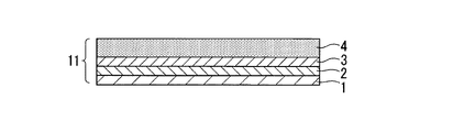
図1に示した本発明のFPC用電磁波シールド材10は、基材1が可撓性を有する厚みが1〜9μm、水蒸気透過度が500g/m2・day以上の溶剤可溶性ポリイミドを用いて形成されたポリイミドフィルムの薄膜樹脂フィルムであり、基材1の一方の面に支持体フィルム6が積層されており、基材1の他方の面に導電性ペースト層3と基材1との密着力を向上させる接着剤層2、導電性微粒子を含有した導電性ペースト層3が順に積層され、さらに、導電性ペースト層3の上に、導電性接着剤層4、剥離フィルム7が順に積層されている。このFPC用電磁波シールド材10は、図2に示すように支持体フィルム6及び剥離フィルム7を除去したFPC用電磁波シールド材11として使用することができる。
The
(ポリイミドフィルム)
本発明に係わるFPC用電磁波シールド材10、11の基材1となる、溶剤可溶性ポリイミドを用いて形成されたポリイミドフィルムの薄膜樹脂フィルムは、ポリイミド樹脂の特徴である高い機械的強度、耐熱性、絶縁性、耐溶剤性を有し、260℃程度までは化学的に安定であるとされている。
ポリイミドとしては、ポリアミック酸を加熱することによる脱水縮合反応で生じる熱硬化型ポリイミドと、非脱水縮合型である溶剤に可溶な溶剤可溶性ポリイミドがある。
一般的なポリイミドフィルムの製造方法として一般的に知られている方法は、極性溶媒中でジアミンとカルボン酸二無水物を反応させることによりイミド前駆体であるポリアミック酸を合成し、ポリアミック酸を熱もしくは触媒を用いることにより脱水環化し対応するポリイミドとするものである。しかし、このイミド化する工程における加熱処理の温度は、200℃〜300℃の温度範囲が好ましいとされ、この温度より加熱温度が低い場合は、イミド化が進まない可能性があるため好ましくなく、上記温度より加熱温度が高い場合は、化合物の熱分解が生じるおそれがあるため好ましくないとされる。
(Polyimide film)
A thin film resin film of a polyimide film formed using a solvent-soluble polyimide, which becomes the base material 1 of the electromagnetic
Examples of polyimide include thermosetting polyimide that is generated by a dehydration condensation reaction by heating polyamic acid, and solvent-soluble polyimide that is soluble in a non-dehydration condensation type solvent.
A generally known method for producing a polyimide film is to synthesize polyamic acid, which is an imide precursor, by reacting diamine and carboxylic dianhydride in a polar solvent, and heat the polyamic acid. Alternatively, a corresponding polyimide is formed by dehydration cyclization by using a catalyst. However, the temperature of the heat treatment in this imidization step is preferably a temperature range of 200 ° C. to 300 ° C., and if the heating temperature is lower than this temperature, imidization may not proceed, which is not preferable. If the heating temperature is higher than the above temperature, the compound may be thermally decomposed, which is not preferable.
本発明のFPC用電磁波シールド材は、基材の可撓性をより向上させることを意図して、厚みが10μm未満の極めて薄いポリイミドフィルムを使用するものである。
本発明では、強度上の補強材として用いる支持体フィルム6の片面の上に、薄いポリイミドフィルムを積層して形成した基材、あるいは、支持体フィルム6を用いないで薄いポリイミドフィルムのみからなる基材、のいずれも使用することができる。
使用するポリイミドフィルムの厚みが、約7μmよりも薄い場合には、強度上の補強材として用いる支持体フィルム6の片面の上に、薄いポリイミドフィルムを積層して形成するのが好ましい。
The electromagnetic wave shielding material for FPC of the present invention uses a very thin polyimide film having a thickness of less than 10 μm with the intention of further improving the flexibility of the substrate.
In the present invention, a base material formed by laminating a thin polyimide film on one side of a support film 6 used as a reinforcing material for strength, or a base made of only a thin polyimide film without using the support film 6. Any of the materials can be used.
When the thickness of the polyimide film to be used is thinner than about 7 μm, it is preferable to form a thin polyimide film on one surface of the support film 6 used as a reinforcing material for strength.
ところが、ポリイミドフィルム自体には、加熱温度200℃〜250℃での加熱処理に対する耐熱性を有しているが、支持体フィルム6としては、価格と耐熱温度性能との兼ね合いから、汎用の耐熱性樹脂フィルム、例えば、ポリエチレンテレフタレート(PET)樹脂フィルムを使用するため、従来のイミド前駆体であるポリアミック酸からポリイミドを形成する方法を採用することができない。
溶剤可溶性ポリイミドは、そのポリイミドのイミド化が完結していて、且つ溶剤に可溶であるため、溶剤に溶解させた塗布液を塗布した後、200℃未満の低温で溶剤を揮発させることにより、成膜することができる。このため、本発明のFPC用電磁波シールド材に使用される基材1は、支持体フィルム6の片面の上に、非脱水縮合型である溶剤可溶性ポリイミドの塗布液を塗布した後、温度を200℃未満の加熱温度で乾燥させて、溶剤可溶性ポリイミドを用いて形成されたポリイミドフィルムの薄膜樹脂フィルムを形成することが好ましい。こうすることによって、汎用の耐熱性樹脂フィルムからなる支持体フィルム6の片面の上に、厚みが1〜9μmの極めて薄いポリイミドフィルムを積層することができる。支持体フィルム6をその長手方向に沿って搬送しながら、その上に基材1、接着剤層2、導電性ペースト層3等を連続的に形成することができるので、ロールtoロールでの生産も可能である。
本発明に使用する、非脱水縮合型である溶剤可溶性ポリイミドは、特には限定されないが、市販されている溶剤可溶性ポリイミドの塗布液を使用することが可能である。市販の溶剤可溶性ポリイミドの塗布液としては、具体的には、ソルピー6,6−PI(ソルピー工業)、Q−IP−0895D(ピーアイ技研)、PIQ(日立化成工業)、SPI−200N(新日鉄化学)、リカコートSN−20、リカコートPN−20(新日本理化)などを挙げることができる。溶剤可溶性ポリイミドの塗布液を、支持体フィルム6の上に塗布する方法は、特に制限されず、例えば、ダイコーター、ナイフコーター、リップコーター等のコーターにて塗布することが可能である。
However, although the polyimide film itself has heat resistance against heat treatment at a heating temperature of 200 ° C. to 250 ° C., the support film 6 is a general-purpose heat resistance because of the balance between price and heat resistance temperature performance. Since a resin film, for example, a polyethylene terephthalate (PET) resin film is used, a method of forming polyimide from polyamic acid which is a conventional imide precursor cannot be employed.
The solvent-soluble polyimide is complete in imidization of the polyimide and is soluble in the solvent. After applying the coating solution dissolved in the solvent, the solvent is volatilized at a low temperature of less than 200 ° C. A film can be formed. For this reason, the base material 1 used for the electromagnetic wave shielding material for FPC of the present invention is coated with a non-dehydration-condensation solvent-soluble polyimide coating solution on one surface of the support film 6, and then the temperature is 200. It is preferable to dry at a heating temperature of less than 0 ° C. to form a thin film resin film of a polyimide film formed using a solvent-soluble polyimide. By carrying out like this, the very thin polyimide film whose thickness is 1-9 micrometers can be laminated | stacked on the single side | surface of the support body film 6 which consists of a general purpose heat resistant resin film. Since the substrate 1, the adhesive layer 2, the
The solvent-soluble polyimide that is a non-dehydrating condensation type used in the present invention is not particularly limited, but a commercially available coating solution for solvent-soluble polyimide can be used. Specific examples of commercially available solvent-soluble polyimide coating solutions include Solpy 6,6-PI (Solpy Industry), Q-IP-0895D (PI Engineering), PIQ (Hitachi Chemical Industry), SPI-200N (Nippon Steel Chemical). ), Rika Coat SN-20, Rika Coat PN-20 (New Nippon Rika) and the like. The method for applying the solvent-soluble polyimide coating solution on the support film 6 is not particularly limited, and can be applied by a coater such as a die coater, a knife coater, or a lip coater.
本発明で使用するポリイミドフィルムの厚みは、1〜9μmであることが好ましい。ポリイミドフィルムの厚みを0.8μm未満に製膜するのは、製膜された膜の機械的な強度が弱いことから技術的に困難である。また、ポリイミドフィルムの厚みが10μmを越えると、優れた屈曲性能を有するFPC用電磁波シールド材11を得ることが困難となる。
また、使用するポリイミドフィルムの厚みが、約7μmよりも薄い場合には、ロールに巻取る時のテンション調整が難しいため、強度上の補強材として用いる支持体フィルム6の片面の上に、薄いポリイミドフィルムを積層して形成されているのが好ましい。
支持体フィルム6を用いないで、薄いポリイミドフィルムのみからなる基材を用いる場合の厚みは、約7〜9μmであることが好ましい。
The thickness of the polyimide film used in the present invention is preferably 1 to 9 μm. Forming a polyimide film with a thickness of less than 0.8 μm is technically difficult because the mechanical strength of the formed film is weak. Moreover, when the thickness of a polyimide film exceeds 10 micrometers, it will become difficult to obtain the electromagnetic
Further, when the thickness of the polyimide film to be used is thinner than about 7 μm, it is difficult to adjust the tension at the time of winding on a roll. Therefore, a thin polyimide film is formed on one side of the support film 6 used as a reinforcing material for strength. It is preferably formed by laminating films.
The thickness in the case of using a substrate made of only a thin polyimide film without using the support film 6 is preferably about 7 to 9 μm.
また、本発明で使用するポリイミドフィルムの水蒸気透過度は、500g/m2・day以上であることが好ましい。500g/m2・dayよりも水蒸気透過度が低い場合には、FPCを被覆した後の、はんだリフローのような加熱工程において、各層の残留溶剤や接着剤からのアウトガス、フィルム中の水分が急激に熱せられることによって発生する水蒸気により各層間が剥離してしまう可能性がある。水蒸気透過度には特に上限を設けないが、同じ材料を使用する限り、水蒸気透過度は厚みに反比例するので、厚みを薄くして水蒸気透過度を上げる場合には、上述した厚みの範囲に収まることが好ましい。 The water vapor permeability of the polyimide film used in the present invention is preferably 500 g / m 2 · day or more. When the water vapor permeability is lower than 500 g / m 2 · day, in the heating process such as solder reflow after coating the FPC, the outgas from the residual solvent and adhesive of each layer and the moisture in the film are abrupt. Each layer may be peeled off by water vapor generated by being heated. There is no particular upper limit to the water vapor transmission rate, but as long as the same material is used, the water vapor transmission rate is inversely proportional to the thickness. Therefore, when the water vapor transmission rate is increased by reducing the thickness, the water vapor transmission rate falls within the above range. It is preferable.
(支持体フィルム)
本発明に使用する支持体フィルム6の基材としては、例えば、ポリエチレンテレフタレート、ポリブチレンテレフタレート、ポリエチレンナフタレート等のポリエステルフィルム、ポリプロピレンやポリエチレン等のポリオレフィンフィルムが挙げられる。
支持体フィルム6の基材が、例えば、ポリエチレンテレフタレートなどの、基材自体にある程度の剥離性を有している場合には、支持体フィルム6の上に、剥離処理を施さなくて、直接に、塗布された誘電体の薄膜樹脂フィルムからなる基材1を積層してもよいし、基材1をより剥離し易くするための剥離処理を、支持体フィルム6の表面に施してもよい。
また、上記の支持体フィルム6として用いる基材フィルムが、剥離性を有していない場合には、アミノアルキッド樹脂やシリコーン樹脂等の剥離剤を塗布した後、加熱乾燥することにより、剥離処理が施される。本発明のFPC用電磁波シールド材10、11は、FPCに貼り合わされるので、この剥離剤には、シリコーン樹脂を使用しないことが望ましい。なぜならシリコーン樹脂を剥離剤として用いると、支持体フィルム6の表面に接触した基材1の表面に、シリコーン樹脂の一部が移行し、さらにFPC用電磁波シールド材11の内部を通じて基材1から導電性接着剤層4へと移行する恐れがある。この導電性接着剤層4の表面に移行したシリコーン樹脂が、導電性接着剤層4の接着力を弱めたりする恐れがあるためである。本発明に使用される支持体フィルム6の厚みは、FPCに被覆して使用する際のFPC用電磁波シールド材11の全体の厚みからは除外されるので、特に限定されないが、通常12〜150μm程度である。
(Support film)
Examples of the substrate of the support film 6 used in the present invention include polyester films such as polyethylene terephthalate, polybutylene terephthalate, and polyethylene naphthalate, and polyolefin films such as polypropylene and polyethylene.
When the base material of the support film 6 has a certain degree of peelability on the base material itself, such as polyethylene terephthalate, for example, it is directly applied to the support film 6 without performing a peeling treatment. The base material 1 made of an applied dielectric thin film resin film may be laminated, or the surface of the support film 6 may be subjected to a peeling treatment for making the base material 1 easier to peel off.
Moreover, when the base film used as the support film 6 does not have releasability, a release treatment such as amino alkyd resin or silicone resin is applied and then dried by heating. Applied. Since the electromagnetic
(接着剤層)
本発明のFPC用電磁波シールド材10、11に用いられる接着剤層2は、基材1であるポリイミドフィルムの薄膜と導電性ペースト層3との密着力の向上を図るために、設けるものである。
接着剤層2は、その上に積層される導電性ペースト層3の焼成温度が150〜250℃であるために、耐熱性に優れた接着剤を用いる必要がある。また、基材1となるポリイミドフィルムと導電性ペースト層3に対する接着力に優れている必要がある。
接着剤層2に用いられる接着性樹脂組成物としては、好ましくは、ポリエステル樹脂、ポリウレタン樹脂、(メタ)アクリル樹脂、ポリエチレン樹脂、ポリスチレン樹脂、ポリアミド樹脂などの熱可塑性樹脂が用いられる。また、エポキシ樹脂、アミノ樹脂、ポリイミド樹脂、(メタ)アクリル樹脂などの熱硬化型であってもよい。
接着剤層2の接着性樹脂組成物として特に好ましいのは、エポキシ基を有するポリエステル系樹脂組成物を架橋させる接着性樹脂組成物や、ポリウレタン系樹脂に硬化剤としてエポキシ樹脂を混ぜた接着性樹脂組成物である。このため、接着剤層2は、ポリイミドフィルムの薄膜からなる基材1よりも、硬い物性を有している。エポキシ基を有するポリエステル系樹脂組成物は、特に限定されるものではないが、例えば1分子に2個以上のエポキシ基を有するエポキシ樹脂(その未硬化樹脂)と、1分子に2個以上のカルボキシル基を有する多価カルボン酸との反応等により得ることができる。エポキシ基を有するポリエステル系樹脂組成物の架橋は、エポキシ基と反応するエポキシ樹脂用の架橋剤を用いることができる。
(Adhesive layer)
The adhesive layer 2 used for the electromagnetic
Since the firing temperature of the
As the adhesive resin composition used for the adhesive layer 2, a thermoplastic resin such as a polyester resin, a polyurethane resin, a (meth) acrylic resin, a polyethylene resin, a polystyrene resin, or a polyamide resin is preferably used. Moreover, thermosetting types, such as an epoxy resin, an amino resin, a polyimide resin, (meth) acrylic resin, may be sufficient.
Particularly preferred as the adhesive resin composition for the adhesive layer 2 is an adhesive resin composition for crosslinking a polyester resin composition having an epoxy group, or an adhesive resin in which an epoxy resin is mixed as a curing agent with a polyurethane resin. It is a composition. For this reason, the adhesive bond layer 2 has a harder physical property than the base material 1 which consists of a thin film of a polyimide film. The polyester-based resin composition having an epoxy group is not particularly limited. For example, an epoxy resin having two or more epoxy groups per molecule (its uncured resin) and two or more carboxyls per molecule. It can be obtained by reaction with a polyvalent carboxylic acid having a group. For crosslinking of the polyester-based resin composition having an epoxy group, a crosslinking agent for epoxy resin that reacts with the epoxy group can be used.
また、接着剤層2は、カーボンブラック、黒鉛、アニリンブラック、シアニンブラック、チタンブラック、黒色酸化鉄、酸化クロム、酸化マンガンからなる群より選択される1種以上の黒色顔料又は着色顔料からなる光吸収材を含んでいてもよい。
カーボンブラックなどの黒色顔料を混ぜ込むのが好ましい。黒色顔料又は着色顔料からなる光吸収材は、接着剤層2の中に0.1〜30重量%で含有させるのが好ましい。黒色顔料又は着色顔料は、SEM観察による一次粒子の平均粒径が0.02〜0.1μm程度であることが好ましい。
また、黒色顔料としては、シリカ粒子などを黒の色材に浸漬させて表層部のみを黒色にしてもよいし、黒色の着色樹脂などから形成して全体にわたって黒色からなるようにしてもよい。また、黒色顔料は、真黒以外に灰色、黒っぽい茶色、又は黒っぽい緑色などの黒色に近似した色を呈する粒子を含み、光を反射しにくい暗色であれば使用することができる。
接着剤層2の厚みは、0.05〜1μm程度であることが好ましく、この程度の膜厚であれば、導電性ペースト層3との充分な密着力が得られる。接着剤層2の厚みが、0.05μm以下の場合は、光吸収材の微粒子が表出してしまい、基材1と導電性ペースト層3との密着力が低下する恐れがある。また、接着剤層2の厚みが1μmを超えても、ポリイミドフィルムからなる基材1や導電性ペースト層3に対する接着力の増加には効果がないから、接着剤層2の厚みが1μmを超えるのはコストが増大するので好ましくない。
The adhesive layer 2 is a light composed of one or more black pigments or colored pigments selected from the group consisting of carbon black, graphite, aniline black, cyanine black, titanium black, black iron oxide, chromium oxide, and manganese oxide. An absorbent material may be included.
It is preferable to mix a black pigment such as carbon black. The light absorbing material made of a black pigment or a colored pigment is preferably contained in the adhesive layer 2 at 0.1 to 30% by weight. The black pigment or the colored pigment preferably has an average primary particle size of about 0.02 to 0.1 μm by SEM observation.
Moreover, as a black pigment, a silica particle etc. may be immersed in a black color material, and only a surface layer part may be made black, and it may be formed from a black colored resin etc. and may become black over the whole. Further, the black pigment includes particles exhibiting a color similar to black, such as gray, dark brown, or dark green, in addition to true black, and can be used as long as it is a dark color that hardly reflects light.
The thickness of the adhesive layer 2 is preferably about 0.05 to 1 μm, and if the thickness is about this level, sufficient adhesion with the
(導電性ペースト層)
本発明に用いる導電性ペースト層3は、導電性フィラーをバインダーとなる樹脂組成物に混ぜ込んだ導電性ペーストが用いられる。
導電性ペーストとしては、導電性金属微粒子、カーボンナノチューブ、カーボンナノファイバーからなる導電性フィラー群の中から選択された1つ以上と、バインダー樹脂組成物とを含むことが好ましい。導電性金属微粒子としては、銅、銀、ニッケル、アルミニウム等の金属微粉末が用いられるが、導電性能が高く、価格が安価であることから銅または銀の微粉末やナノ粒子を用いるのが好ましい。また、導電性を有するカーボンナノ粒子である、カーボンナノチューブ、カーボンナノファイバーも使用することができる。
導電性ペースト層3の焼成後の体積抵抗率は、1.5×10⁻⁵Ω・cm以下であることが望ましい。また、導電性ペースト層3の焼成後の表面抵抗率は、0.2Ω/□以下であることが望ましい。
(Conductive paste layer)
As the
The conductive paste preferably contains one or more selected from the group of conductive fillers composed of conductive metal fine particles, carbon nanotubes, and carbon nanofibers, and a binder resin composition. As the conductive metal fine particles, fine metal powders such as copper, silver, nickel, and aluminum are used, but it is preferable to use fine powders or nanoparticles of copper or silver because of their high conductive performance and low price. . In addition, carbon nanotubes and carbon nanofibers, which are carbon nanoparticles having conductivity, can also be used.
The volume resistivity of the
導電性ペーストの焼成温度を150〜250℃の温度範囲の低温に抑えるためには、金属微粒子の平均粒子径が1〜120nmの範囲であることが好ましく、1〜100nmの範囲がより好ましい。
本発明に係わるFPC用電磁波シールド材10、11の導電性ペースト層3は、このような金属微粒子を含有することにより、薄膜化に対応することが可能となるだけでなく、微粒子同士が融着して導電率の向上も同時に実現できる。本発明に使用される導電性ペーストは、分散溶媒中に、例えば、平均粒子径が1〜120nmの範囲の金属微粒子を均一に分散させるため、この金属微粒子表面を有機分子層で被覆して、溶媒中での分散性能を向上させるのが好ましい。最終的に、導電性ペーストの加熱焼成工程において、金属微粒子相互が表面を接触させ、導電性ペースト層3の導電性を得ることができる。
導電性ペーストの加熱焼成は、例えば、150〜250℃程度に加熱することにより、金属微粒子の表面を被覆している有機分子層を離脱させ、蒸散させて除去するため、焼成温度を有機分子層の沸点範囲にするのが好ましい。
上述したように、基材1となるポリイミドフィルム自体は、加熱温度200℃〜250℃での加熱処理に対する耐熱性を有しているが、支持体フィルム6は耐熱性に劣るため、支持体フィルム6を用いる場合は、焼成温度をより低温とすることが好ましい。
導電性ペーストの焼成温度は、好ましくは150〜180℃であり、これにより支持体フィルム6の熱劣化による外観不良を抑制することができる。
In order to suppress the firing temperature of the conductive paste to a low temperature in the temperature range of 150 to 250 ° C., the average particle diameter of the metal fine particles is preferably in the range of 1 to 120 nm, and more preferably in the range of 1 to 100 nm.
The
The conductive paste is heated and fired, for example, by heating to about 150 to 250 ° C., the organic molecular layer covering the surface of the metal fine particles is separated and evaporated to remove the organic paste. Preferably, the boiling point is within the range.
As described above, the polyimide film itself serving as the base material 1 has heat resistance to heat treatment at a heating temperature of 200 ° C. to 250 ° C., but the support film 6 is inferior in heat resistance, and thus the support film. When 6 is used, it is preferable that the firing temperature is lower.
The firing temperature of the conductive paste is preferably 150 to 180 ° C., whereby the appearance defect due to thermal deterioration of the support film 6 can be suppressed.
導電性ペーストに、導電性フィラーと混合して用いられるバインダー樹脂組成物としては、好ましくは、ポリエステル樹脂、(メタ)アクリル樹脂、ポリエチレン樹脂、ポリスチレン樹脂、ポリアミド樹脂などの熱可塑性樹脂が用いられる。また、エポキシ樹脂、アミノ樹脂、ポリイミド樹脂、(メタ)アクリル樹脂などの熱硬化性樹脂であってもよい。
導電性ペーストは、これらのバインダー樹脂組成物に、導電性金属微粒子、カーボンナノチューブ、カーボンナノファイバーなどの導電性フィラーを混ぜ込んだ後に、必要に応じてアルコールやエーテルなどの有機溶剤を加えて粘度調整を行う。粘度調整は、有機溶剤の添加量(配合比)によって行うことができる。
導電性ペースト層3の焼成した後の厚みは、0.1〜2μm程度であることが好ましい。さらに好ましくは、0.3〜1μm程度の厚みであることが望ましい。導電性ペースト層3の焼成した後の厚みが0.1μmよりも薄い場合は、高い電磁波シールド性能を得ることが困難である。一方、導電性ペースト層3の焼成した後の厚みが2μmよりも厚いと、支持体フィルム6及び剥離フィルム7を除いた、FPC用電磁波シールド材11の全体の厚みを、25μm以下に抑えることが困難となる。
As the binder resin composition used by mixing the conductive paste with the conductive filler, a thermoplastic resin such as a polyester resin, a (meth) acrylic resin, a polyethylene resin, a polystyrene resin, or a polyamide resin is preferably used. Moreover, thermosetting resins, such as an epoxy resin, an amino resin, a polyimide resin, and a (meth) acrylic resin, may be sufficient.
The conductive paste is mixed with these binder resin compositions with conductive fillers such as conductive metal fine particles, carbon nanotubes, and carbon nanofibers, and then added with an organic solvent such as alcohol or ether as necessary. Make adjustments. Viscosity adjustment can be performed by the addition amount (blending ratio) of an organic solvent.
The thickness of the
(導電性接着剤層)
本発明に係わるFPC用電磁波シールド材10、11の、導電性ペースト層3の上に積層される導電性接着剤としては、アクリル系接着剤、ポリウレタン系接着剤、エポキシ系接着剤、ゴム系接着剤、シリコーン系接着剤等の、一般的に使用されている熱硬化型接着剤に、導電性の微粒子や4級アンモニウム塩などのイオン化合物、導電性高分子などを混ぜて導電性を持たせたものが使用されるが、特に限定されない。
導電性接着剤は、常温で感圧接着性を示す粘着剤ではなく、加熱加圧による接着剤であると、繰り返しの屈曲に対して接着力が低下しにくくなり好ましい。
導電性接着剤層4に配合する導電性の微粒子は、特に限定はされず、従来から公知のものを適用できる。例えば、カーボンブラックや、銀、ニッケル、銅、アルミニウムなどの金属からなる金属微粒子、及びそれらの金属微粒子の表面に他の金属を被覆した複合金属微粒子があげられ、これらの1種または2種以上を適宜選択して用いることができる。
また、上記の導電性接着剤においては、優れた導電性を得るために、導電性物質粒子相互の接触、および該粒子と導電性ペースト層および被着体であるFPCとの接触が良くなるように、導電性物質を多量に含有させると接着力が低下する。一方、接着力を高めるために導電性物質の含有量を低減すると、導電性物質と導電性ペースト層および被着体であるFPCとの接触が不十分となって、導電性が低下するという、相反する問題がある。このため、導電性微粒子の配合量は、接着剤(固形分)100重量部に対して、通常、0.5〜50重量部程度、より好ましくは2〜10重量部である。
(Conductive adhesive layer)
As the conductive adhesive laminated on the
It is preferable that the conductive adhesive is not a pressure-sensitive adhesive exhibiting pressure-sensitive adhesiveness at room temperature but an adhesive by heating and pressurization because the adhesive force is unlikely to decrease with respect to repeated bending.
The electroconductive fine particles mix | blended with the electroconductive adhesive layer 4 are not specifically limited, A conventionally well-known thing can be applied. Examples thereof include metal fine particles made of metal such as carbon black, silver, nickel, copper, and aluminum, and composite metal fine particles obtained by coating the surface of the metal fine particles with other metals. Can be appropriately selected and used.
Further, in the above conductive adhesive, in order to obtain excellent conductivity, the contact between the conductive material particles and the contact between the particles, the conductive paste layer, and the FPC as the adherend are improved. In addition, if a large amount of conductive material is contained, the adhesive strength is reduced. On the other hand, when the content of the conductive material is reduced in order to increase the adhesive force, the contact between the conductive material and the conductive paste layer and the FPC that is the adherend becomes insufficient, and the conductivity decreases. There are conflicting problems. For this reason, the compounding quantity of electroconductive fine particles is about 0.5-50 weight part normally with respect to 100 weight part of adhesive agents (solid content), More preferably, it is 2-10 weight part.
また、本発明の導電性接着剤層4を構成する導電性接着剤としては、導電性微粒子を含んだ異方導電性接着剤が好ましく、公知のものを使用できる。この異方導電性接着剤としては、例えば、エポキシ樹脂等の絶縁性の熱硬化性樹脂を主成分とし、導電性微粒子が分散された接着剤が使用できる。
また、異方導電性接着剤に使用される導電性微粒子としては、例えば、金、銀、亜鉛、錫、半田等の金属微粒子の単体もしくは2種以上を組み合わせても良い。また、導電性微粒子としては、金属でめっきされた樹脂粒子を使用できる。導電性微粒子の形状は、微細な粒子が直鎖状に繋がった形状、あるいは針形状を有するのが好ましい。このような形状であれば、圧着部材によりFPCに対して加熱加圧処理を行う際に、低い加圧力で導電性微粒子がFPCの導体配線に噛み込むことが可能になる。
異方導電性接着剤は、FPCとの接続抵抗値が5Ω/cm以下からなるのが好ましい。
Moreover, as a conductive adhesive which comprises the conductive adhesive layer 4 of this invention, the anisotropic conductive adhesive containing conductive fine particles is preferable, and a well-known thing can be used. As this anisotropic conductive adhesive, for example, an adhesive having an insulating thermosetting resin such as an epoxy resin as a main component and conductive fine particles dispersed therein can be used.
In addition, as the conductive fine particles used for the anisotropic conductive adhesive, for example, single or two or more kinds of metal fine particles such as gold, silver, zinc, tin, and solder may be combined. Further, as the conductive fine particles, resin particles plated with metal can be used. The shape of the conductive fine particles is preferably a shape in which fine particles are connected in a straight chain or a needle shape. If it is such a shape, when heat-pressing processing with respect to FPC by a crimping | compression-bonding member, it will become possible for electroconductive fine particles to bite into the conductor wiring of FPC with a low pressurizing force.
The anisotropic conductive adhesive preferably has a connection resistance value with the FPC of 5 Ω / cm or less.
導電性接着剤の接着力は、特に制限を受けないが、その測定方法はJIS Z 0237に記載の試験方法に準ずる。被着体表面に対する接着力が剥離角度180度ピール、剥離速度300mm/分の条件下で、5〜30N/インチの範囲が好適である。接着力が5N/インチ未満では、例えば、FPCに貼り合せた電磁波シールド材が剥がれたり浮いたりする場合がある。
FPCに対する加熱加圧接着の条件は、特に限定されるものではないが、例えば温度を160℃、加圧力を2.54MPaとして30分間熱プレスすることが好ましい。
The adhesive strength of the conductive adhesive is not particularly limited, but the measurement method is in accordance with the test method described in JIS Z 0237. A range of 5 to 30 N / inch is preferable under the condition that the adhesive strength to the adherend surface is a peeling angle of 180 ° peel and a peeling speed of 300 mm / min. When the adhesive force is less than 5 N / inch, for example, the electromagnetic wave shielding material bonded to the FPC may peel off or float.
The conditions for heat and pressure adhesion to the FPC are not particularly limited, but for example, it is preferable to heat-press for 30 minutes at a temperature of 160 ° C. and a pressure of 2.54 MPa.
(剥離フィルム)
剥離フィルム7の基材としては、例えば、ポリエチレンテレフタレート、ポリブチレンテレフタレート、ポリエチレンナフタレート等のポリエステルフィルム、ポリプロピレンやポリエチレン等のポリオレフィンフィルムが挙げられる。これらの基材フィルムに、アミノアルキッド樹脂やシリコーン樹脂等の剥離剤を塗布した後、加熱乾燥することにより、剥離処理が施される。本発明のFPC用電磁波シールド材10、11は、FPCに貼り合わされるので、この剥離剤には、シリコーン樹脂を使用しないことが望ましい。なぜならシリコーン樹脂を剥離剤として用いると、剥離フィルム7の表面に接触した導電性接着剤層4の表面に、シリコーン樹脂の一部が移行し、さらにFPC用電磁波シールド材11の内部を通じて導電性接着剤層4から基材1へと移行する恐れがある。この導電性接着剤層4の表面に移行したシリコーン樹脂が導電性接着剤層4の接着力を弱めたりする恐れがあるためである。本発明に使用される剥離フィルム7の厚みは、FPCに被覆して使用する際のFPC用電磁波シールド材11の全体の厚みからは除外されるので、特に限定されないが、通常12〜150μm程度である。
(Peeling film)
Examples of the substrate of the release film 7 include polyester films such as polyethylene terephthalate, polybutylene terephthalate, and polyethylene naphthalate, and polyolefin films such as polypropylene and polyethylene. After applying a release agent such as amino alkyd resin or silicone resin to these base films, the release treatment is performed by drying by heating. Since the electromagnetic
本発明のFPC用電磁波シールド材10、11は、繰り返しての屈曲動作を受けるFPCに貼り合せて使用することが可能な、屈曲特性に優れたFPC用電磁波シールド材として好適に用いることができる。また、本発明のFPC用電磁波シールド材は、電磁波遮蔽用の部材として携帯電話や電子機器に使用することができる。
The electromagnetic
以下、実施例により、本発明を具体的に説明する。
(実施例1)
厚みが50μmのポリエチレンテレフタレート(PET)フィルム(東洋紡株式会社製、品番:E5100)を、支持体フィルム6として用いた。その支持体フィルム6の片面の上に、厚さ33μmのときの水蒸気透過度が180g/m2・dayである溶剤可溶性ポリイミドの塗布液を、乾燥後の厚みが4μmになるように流延塗布、乾燥させて、誘電体の薄膜樹脂フィルムからなる基材1を積層した。形成された基材1の上に、光吸収材の黒色顔料としてカーボンブラックと、耐熱温度が260〜280℃のポリエステル系樹脂組成物とを混ぜた、接着剤層2を形成するための塗工液を用いて、乾燥後の厚みが0.3μmとなるように塗布して接着剤層2を積層した。接着剤層2の上に、導電性フィラーとして、一次平均粒子径が約50nmの銀粒子を混ぜて調製した導電性ペーストを用いて、乾燥後の厚みが0.3μmとなるように塗布した後、温度150℃にて焼成して導電性ペースト層3を形成した。導電性ペースト層3の上に、エポキシ系熱硬化型の導電性接着剤を乾燥後の厚みが12〜18μmとなるように塗布して導電性接着剤層4を形成し、実施例1のFPC用電磁波シールド材を得た。焼成後の導電性ペースト層3の体積抵抗率を測定した値は、1.5×10−5Ω・cm以下であった。
Hereinafter, the present invention will be described specifically by way of examples.
Example 1
A polyethylene terephthalate (PET) film (product number: E5100, manufactured by Toyobo Co., Ltd.) having a thickness of 50 μm was used as the support film 6. On one side of the support film 6, a solvent-soluble polyimide coating solution having a water vapor permeability of 180 g / m 2 · day at a thickness of 33 μm is cast so that the thickness after drying becomes 4 μm. The substrate 1 made of a dielectric thin film resin film was laminated. Coating for forming an adhesive layer 2 in which carbon black as a light-absorbing material black pigment and a polyester resin composition having a heat-resistant temperature of 260 to 280 ° C. are mixed on the formed substrate 1. Using the solution, the adhesive layer 2 was laminated by coating so that the thickness after drying was 0.3 μm. After applying onto the adhesive layer 2 using a conductive paste prepared by mixing silver particles having a primary average particle diameter of about 50 nm as a conductive filler so that the thickness after drying is 0.3 μm. The
(実施例2)
溶剤可溶性ポリイミドの塗布液を、乾燥後の厚みが6μmになるように流延塗布、乾燥させて、誘電体の薄膜樹脂フィルムからなる基材1を積層した以外は、実施例1と同様にして、実施例2の電磁波シールド材を得た。
(Example 2)
A solvent-soluble polyimide coating solution was casted and dried so that the thickness after drying was 6 μm, and the same procedure as in Example 1 was performed except that a base material 1 made of a dielectric thin film resin film was laminated. The electromagnetic shielding material of Example 2 was obtained.
(実施例3)
溶剤可溶性ポリイミドの塗布液を、乾燥後の厚みが8μmになるように流延塗布、乾燥させて、誘電体の薄膜樹脂フィルムからなる基材1を積層した以外は、実施例1と同様にして、実施例3の電磁波シールド材を得た。
(Example 3)
A solvent-soluble polyimide coating solution was casted and dried so that the thickness after drying was 8 μm, and the substrate 1 made of a dielectric thin film resin film was laminated. The electromagnetic shielding material of Example 3 was obtained.
(比較例1)
支持体フィルム6を用いず、基材1として厚みが10μmの熱硬化型ポリイミドからなるポリイミドフィルムを用いた以外は、実施例1と同様にして、比較例1のFPC用電磁波シールド材を得た。
(Comparative Example 1)
An electromagnetic wave shielding material for FPC of Comparative Example 1 was obtained in the same manner as in Example 1 except that the support film 6 was not used and a polyimide film made of thermosetting polyimide having a thickness of 10 μm was used as the substrate 1. .
(比較例2)
溶剤可溶性ポリイミドの塗布液を、乾燥後の厚みが18μmになるように流延塗布、乾燥させて、誘電体の薄膜樹脂フィルムからなる基材1を積層した以外は、実施例1と同様にして、比較例2の電磁波シールド材を得た。
(Comparative Example 2)
A solvent-soluble polyimide coating solution was cast and dried so that the thickness after drying was 18 μm, and the substrate 1 made of a dielectric thin film resin film was laminated. The electromagnetic shielding material of Comparative Example 2 was obtained.
(比較例3)
溶剤可溶性ポリイミドの塗布液を、乾燥後の厚みが24μmになるように流延塗布、乾燥させて、誘電体の薄膜樹脂フィルムからなる基材1を積層した以外は、実施例1と同様にして、比較例3の電磁波シールド材を得た。
(Comparative Example 3)
A solvent-soluble polyimide coating solution was casted and dried so that the thickness after drying was 24 μm, and the substrate 1 made of a dielectric thin film resin film was laminated. The electromagnetic shielding material of Comparative Example 3 was obtained.
(基材の水蒸気透過度測定方法)
実施例1、2、3、及び比較例2,3記載の溶剤可溶性ポリイミドの水蒸気透過度は以下のようにして求めた。
厚みが50μmのポリエチレンテレフタレート(PET)フィルム(東洋紡株式会社製、品番:E5100)を、支持体フィルム6として用いた。その支持体フィルム6の片面の上に、溶剤可溶性ポリイミドの塗布液を、乾燥後の厚みが33μmになるように流延塗布、乾燥させて、誘電体の薄膜樹脂フィルムからなる基材1を積層した。
支持体フィルム6から薄膜樹脂フィルムからなる基材1を剥離し、JIS−K−7129 B法「赤外線センサ法による水蒸気透過度の求め方」に従い測定したところ、180g/m2・dayであった。水蒸気透過度は、測定対象の厚みに反比例することが知られており、実施例1、2、3、及び比較例2,3記載の溶剤可溶性ポリイミドの水蒸気透過度は、厚み33μmのときの結果を元に、計算で求めた。
比較例1は、基材1として用いた、厚みが10μmの熱硬化型ポリイミドからなるポリイミドフィルムの水蒸気透過度を、そのまま上述した測定方法で測定した。
(Measurement method of water vapor permeability of substrate)
The water vapor permeability of the solvent-soluble polyimides described in Examples 1, 2, and 3 and Comparative Examples 2 and 3 was determined as follows.
A polyethylene terephthalate (PET) film (product number: E5100, manufactured by Toyobo Co., Ltd.) having a thickness of 50 μm was used as the support film 6. On one side of the support film 6, a solvent-soluble polyimide coating solution is cast and dried so that the thickness after drying is 33 μm, and the substrate 1 made of a dielectric thin film resin film is laminated. did.
The base material 1 made of a thin film resin film was peeled off from the support film 6 and measured according to JIS-K-7129 B method “How to obtain water vapor transmission rate by infrared sensor method” and found to be 180 g / m 2 · day. . It is known that the water vapor permeability is inversely proportional to the thickness of the object to be measured, and the water vapor permeability of the solvent-soluble polyimides described in Examples 1, 2, and 3 and Comparative Examples 2 and 3 is the result when the thickness is 33 μm. Calculated based on the above.
In Comparative Example 1, the water vapor permeability of a polyimide film made of a thermosetting polyimide having a thickness of 10 μm used as the substrate 1 was directly measured by the measurement method described above.
(導電性ペースト層3の表面抵抗率の測定方法)
JIS−K−7194「導電性プラスチックの4探針法による抵抗率試験方法」の規定に従って、三菱化学(株)製の抵抗率計ロレスターGP T600型で、導電性ペースト層3の表面抵抗率を測定した。
(Method for measuring surface resistivity of conductive paste layer 3)
In accordance with JIS-K-7194 “Resistivity Test Method for Conductive Plastics by Four-Probe Method”, the resistivity meter Lorester GP T600 type manufactured by Mitsubishi Chemical Corporation is used to determine the surface resistivity of the
(屈曲試験の測定方法)
導電性ペースト層3の上に、エポキシ系熱硬化性接着剤(スリーボンド製、品番:33A−798)を用いて、乾燥後の厚みが12μmになるように調整して塗布したものを、テストパターンが設けられたフレキシブルプリント基板に、FPC用電磁波シールド材の導電性接着剤層4側を対向させて重ね、160℃、2.54MPaで30分間熱プレスした後、幅12.7mm×長さ160mmの寸法に裁断して試験片を得た。
IPC規格TM−650「TEST METHODS MANUAL」(JIS−C−6471の参考3「耐屈曲性」)に従って、裁断した試験片を用いて、R=1.5mm又はR=1.0mmの設定条件で、IPC屈曲試験を行い、導電性ペースト層の抵抗値が、導電層の繰り返しての屈曲動作により初期時の抵抗値に比べて2倍に増加する時の、屈曲試験の回数を計測して屈曲性能を評価した。
屈曲試験結果の判定は、屈曲試験により、導電性ペースト層の抵抗値が、導電層の繰り返しての屈曲動作により初期時の抵抗値に比べて2倍に増加する時の、屈曲試験の回数が30万回を越える場合を、合格(○)とし、30万回以下の場合を、不合格(×)とした。
(Measurement method of bending test)
A test pattern was prepared by applying an epoxy thermosetting adhesive (manufactured by ThreeBond, product number: 33A-798) on the
In accordance with IPC standard TM-650 “TEST METHODS MANUAL” (
The determination of the bending test result is based on the bending test, when the resistance value of the conductive paste layer increases twice as much as the initial resistance value due to repeated bending operation of the conductive layer. The case where it exceeded 300,000 times was set to pass (◯), and the case where it was 300,000 times or less was set to fail (x).
(柔軟性試験の測定方法)
屈曲試験に用いるサンプル(幅17mm×長さ160mm)を用いて、(株)東洋精機製作所製のループスティフネステスタにサンプルをセットして測定を開始し、サンプルをループ状に曲げ、そのループの直径方向を押しつぶしたときのロードによって、コシの強弱を評価する。具体的には、屈曲試験に用いるサンプルをループ状に曲げた外側が、電磁波シールド材となるように外周80mmの輪を作り、輪の上側から3.3mm/secのスピードでサンプル部分の短軸の距離が1.5mmとなるまで力を加えて、その状態で5秒間保持した際のサンプルの応力を測定する。
(Measurement method of flexibility test)
Using the sample (width 17 mm x length 160 mm) used for the bending test, the sample was set on a loop stiffness tester manufactured by Toyo Seiki Seisakusyo Co., Ltd., and the measurement was started. The sample was bent into a loop shape, and the diameter of the loop The strength of the stiffness is evaluated by the load when the direction is crushed. Specifically, a ring with an outer circumference of 80 mm is formed so that the outer side of the sample used for the bending test is bent in a loop shape to be an electromagnetic shielding material, and the short axis of the sample portion is formed at a speed of 3.3 mm / sec from the upper side of the ring A force is applied until the distance becomes 1.5 mm, and the stress of the sample when measured for 5 seconds is measured.
(耐熱試験及び耐熱試験後の電磁波シールド材の外観)
FPC用電磁波シールド材の導電性接着剤とポリイミドフィルム(東レ・デュポン製カプトン200H)と対向するように重ね合わせ、160℃、4.5MPa、60分間程、加熱プレスした。2.5cm×10cmに試験片を切り出し、290℃のはんだ浴に10秒間浸漬した後引き上げた。
耐熱試験後の電磁波シールド材の外観は、目視で変形や縮れ等の異常がないかを観察し、異常がなく良好な場合を、合格(○)とし、異常が見られた場合を、不合格(×)とした。
(Appearance of heat shield test and electromagnetic shielding material after heat test)
The conductive adhesive of the electromagnetic wave shielding material for FPC and the polyimide film (Kapton 200H manufactured by Toray DuPont) were superposed and heated and pressed at 160 ° C., 4.5 MPa for about 60 minutes. A test piece was cut out to 2.5 cm × 10 cm, dipped in a solder bath at 290 ° C. for 10 seconds, and then pulled up.
The external appearance of the electromagnetic shielding material after the heat resistance test is visually observed for abnormalities such as deformation and shrinkage. If there is no abnormality and it is good, it is accepted (○). (X).
(試験結果)
実施例1〜3、及び比較例1〜3について、上記の試験方法にて、導電性ペースト層の表面抵抗率、屈曲試験、および柔軟性試験を行い、得られた試験結果を表1に示した。
(Test results)
With respect to Examples 1 to 3 and Comparative Examples 1 to 3, the surface resistivity, the bending test, and the flexibility test of the conductive paste layer were performed by the above test method, and the obtained test results are shown in Table 1. It was.

表1に示した、耐熱試験後の結果によれば、基材1の水蒸気透過度が耐熱試験後の外観に相関があることがわかる。すなわち、基材1の水蒸気透過度が十分に高ければ、急激な加熱による、各層の残留溶剤、接着剤からのアウトガス、フィルム中の水分の気化による、層間の剥離が起こらず、良好な外観を得ることができる。
さらに、実施例1、3によれば、ポリイミドフィルムからなる基材の厚みが1〜9μmであるため、より柔軟性なFPC用電磁波シールド材が得られ、屈曲試験に合格するものとなった。
これらの試験結果から、優れた耐熱性と屈曲性能を有したFPC用電磁波シールド材は、溶剤可溶性ポリイミドを用いて形成されたポリイミドフィルムからなる基材の厚みを1〜9μmの薄膜にすることが必要である。しかし、現在、日本国内において市販されている熱硬化型ポリイミドからなるポリイミドフィルムの厚みとしては、7.5μmが最も薄い規格製品の厚みであるが、本発明のFPC用電磁波シールド材では、その厚みよりも薄くしたポリイミドフィルムを基材に用いることが必要である。そのため、溶剤可溶性ポリイミドの塗布液を薄く流延塗布することによって得られる厚みが1〜9μmのポリイミドフィルムを、基材に使用することによってのみ、優れた屈曲性能に有するFPC用電磁波シールド材を得ることができる。
本発明のFPC用電磁波シールド材は、携帯電話、ノート型パソコン、携帯端末、などの各種の電子機器に、電磁波遮蔽部材として使用することができる。
According to the results after the heat resistance test shown in Table 1, it can be seen that the water vapor permeability of the substrate 1 has a correlation with the appearance after the heat resistance test. That is, if the water vapor permeability of the base material 1 is sufficiently high, no delamination occurs due to rapid heating, residual solvent in each layer, outgas from the adhesive, and vaporization of moisture in the film. Can be obtained.
Furthermore, according to Examples 1 and 3, since the thickness of the base material which consists of a polyimide film is 1-9 micrometers, the more flexible electromagnetic shielding material for FPC was obtained, and it passed the bending test.
From these test results, the electromagnetic shielding material for FPC having excellent heat resistance and bending performance can make the thickness of the substrate made of a polyimide film formed using a solvent-soluble polyimide into a thin film of 1 to 9 μm. is necessary. However, as the thickness of the polyimide film made of thermosetting polyimide that is currently marketed in Japan, 7.5 μm is the thickness of the thinnest standard product. In the electromagnetic wave shielding material for FPC of the present invention, the thickness is as follows. It is necessary to use a thinner polyimide film as the substrate. Therefore, an electromagnetic shielding material for FPC having excellent bending performance can be obtained only by using a polyimide film having a thickness of 1 to 9 μm obtained by thinly casting a solvent-soluble polyimide coating solution as a base material. be able to.
The electromagnetic wave shielding material for FPC of the present invention can be used as an electromagnetic wave shielding member in various electronic devices such as a mobile phone, a notebook computer, and a portable terminal.
1…基材、2…接着剤層、3…導電性ペースト層、4…導電性接着剤層、6…支持体フィルム、7…剥離フィルム、10,11…FPC用電磁波シールド材。 DESCRIPTION OF SYMBOLS 1 ... Base material, 2 ... Adhesive layer, 3 ... Conductive paste layer, 4 ... Conductive adhesive layer, 6 ... Support film, 7 ... Release film, 10, 11 ... Electromagnetic wave shielding material for FPC.
Claims (6)
前記基材が、溶剤可溶性ポリイミドを用いて形成されたポリイミドフィルムからなり、厚みが1〜9μmであり、前記薄膜の接着剤層が、エポキシ基を有するポリエステル系樹脂組成物を架橋させてなり、厚みが0.05〜1μmであり、
前記基材の水蒸気透過度が500g/m2・day以上であることを特徴とするFPC用電磁波シールド材。 On the one side of the support film made of polyethylene terephthalate, substrate made of a thin resin film casting and coating dielectric adhesive layer of the thin film, the conductive paste layer, the conductive adhesive layer, but they are stacked in this order And
The base material is made of a polyimide film formed using a solvent-soluble polyimide, has a thickness of 1 to 9 μm, and the adhesive layer of the thin film is obtained by crosslinking a polyester resin composition having an epoxy group, The thickness is 0.05-1 μm,
An electromagnetic wave shielding material for FPC, wherein the substrate has a water vapor permeability of 500 g / m 2 · day or more.
Priority Applications (3)
| Application Number | Priority Date | Filing Date | Title |
|---|---|---|---|
| JP2011248736A JP5726048B2 (en) | 2011-11-14 | 2011-11-14 | Electromagnetic wave shielding material for FPC |
| KR1020120120267A KR101359474B1 (en) | 2011-11-14 | 2012-10-29 | Electromagnetic wave shield material for fpc |
| CN201210455392.1A CN103108533B (en) | 2011-11-14 | 2012-11-13 | FPC electromagnetic shielding material |
Applications Claiming Priority (1)
| Application Number | Priority Date | Filing Date | Title |
|---|---|---|---|
| JP2011248736A JP5726048B2 (en) | 2011-11-14 | 2011-11-14 | Electromagnetic wave shielding material for FPC |
Publications (3)
| Publication Number | Publication Date |
|---|---|
| JP2013105888A JP2013105888A (en) | 2013-05-30 |
| JP2013105888A5 JP2013105888A5 (en) | 2015-04-09 |
| JP5726048B2 true JP5726048B2 (en) | 2015-05-27 |
Family
ID=48315997
Family Applications (1)
| Application Number | Title | Priority Date | Filing Date |
|---|---|---|---|
| JP2011248736A Active JP5726048B2 (en) | 2011-11-14 | 2011-11-14 | Electromagnetic wave shielding material for FPC |
Country Status (3)
| Country | Link |
|---|---|
| JP (1) | JP5726048B2 (en) |
| KR (1) | KR101359474B1 (en) |
| CN (1) | CN103108533B (en) |
Families Citing this family (21)
| Publication number | Priority date | Publication date | Assignee | Title |
|---|---|---|---|---|
| CN102711428B (en) * | 2012-06-21 | 2015-11-18 | 广州方邦电子有限公司 | Ultra-thin shielding film of a kind of high screening effectiveness and preparation method thereof |
| JP2014046622A (en) * | 2012-08-31 | 2014-03-17 | Dexerials Corp | Transparent conductive body, input device and electronic apparatus |
| US20160120077A1 (en) * | 2013-05-29 | 2016-04-28 | Tatsuta Electric Wire & Cable Co., Ltd. | Electromagnetic wave shield film, printed wiring board using same, and rolled copper foil |
| JP2015012098A (en) * | 2013-06-27 | 2015-01-19 | 住友電工プリントサーキット株式会社 | Shield film and printed wiring board |
| JP6650660B2 (en) * | 2014-01-20 | 2020-02-19 | 東洋インキScホールディングス株式会社 | Electromagnetic wave shielding sheet for flexible printed wiring board and flexible printed wiring board with electromagnetic wave shielding sheet |
| US9553382B2 (en) | 2014-06-27 | 2017-01-24 | Xiaomi Inc. | Headphone socket assembly and electronic equipment including same |
| CN104134907B (en) * | 2014-06-27 | 2017-08-15 | 小米科技有限责任公司 | Phone jack component and electronic equipment |
| JP6520133B2 (en) * | 2015-01-16 | 2019-05-29 | 大日本印刷株式会社 | Laminate, method of manufacturing conductive substrate using the same, and method of manufacturing electronic device |
| JP6520143B2 (en) * | 2015-01-23 | 2019-05-29 | 大日本印刷株式会社 | Laminate, method of manufacturing conductive substrate using the same, method of manufacturing electronic device, and transfer tool |
| KR102527794B1 (en) | 2016-02-04 | 2023-05-03 | 삼성전자주식회사 | Electronic device comprising coil |
| KR20170136063A (en) * | 2016-05-30 | 2017-12-11 | 주식회사 아모그린텍 | Ultra-thin type electromagnetic shielding sheet and electronic apparatus having the same |
| CN107567175A (en) * | 2016-06-30 | 2018-01-09 | 蔡见明 | A kind of electromagnetic shielding film |
| JP2018010888A (en) * | 2016-07-11 | 2018-01-18 | 藤森工業株式会社 | Electromagnetic wave shield material |
| CN110072961B (en) * | 2016-12-22 | 2022-02-08 | 东亚合成株式会社 | Adhesive composition, and cover film, adhesive sheet, copper-clad laminate and electromagnetic wave shielding material using same |
| CN208570149U (en) * | 2018-09-13 | 2019-03-01 | 重庆惠科金渝光电科技有限公司 | Insulating coating, soft arranging wire and display device |
| CN109627704A (en) * | 2018-11-21 | 2019-04-16 | 惠州市串联电子科技有限公司 | Heat-resisting material for FPC substrate |
| JP6699784B2 (en) * | 2019-04-26 | 2020-05-27 | 大日本印刷株式会社 | Laminated body, method of manufacturing conductive substrate using the same, method of manufacturing electronic device, and transfer tool |
| JP6699783B2 (en) * | 2019-04-26 | 2020-05-27 | 大日本印刷株式会社 | Laminated body, method of manufacturing conductive substrate using the same, and method of manufacturing electronic device |
| JP6849131B2 (en) * | 2020-04-30 | 2021-03-24 | 大日本印刷株式会社 | Laminates, methods for manufacturing conductive substrates using them, methods for manufacturing electronic devices, and transfer tools |
| JP6849130B2 (en) * | 2020-04-30 | 2021-03-24 | 大日本印刷株式会社 | A method for manufacturing a laminate and a conductive base material using the same, and a method for manufacturing an electronic device. |
| CN111968857B (en) * | 2020-08-28 | 2022-02-08 | 电子科技大学 | Method for realizing dielectric film double-layer compounding by improving film adhesive force through chemical method |
Family Cites Families (16)
| Publication number | Priority date | Publication date | Assignee | Title |
|---|---|---|---|---|
| JPH07122883A (en) * | 1993-10-21 | 1995-05-12 | Nitto Denko Corp | Electromagnetic-wave shielding material |
| JP4156233B2 (en) * | 2001-12-19 | 2008-09-24 | 大日本印刷株式会社 | Electromagnetic shielding material and flat cable with electromagnetic shielding |
| JP4737656B2 (en) * | 2002-06-24 | 2011-08-03 | 大日本印刷株式会社 | Conductive decorative sheet |
| JP4174248B2 (en) * | 2002-07-01 | 2008-10-29 | 群栄化学工業株式会社 | Polyimide resin, resin composition containing the same, coating material for electronic component, and adhesive for electronic component |
| JP4201548B2 (en) * | 2002-07-08 | 2008-12-24 | タツタ電線株式会社 | SHIELD FILM, SHIELD FLEXIBLE PRINTED WIRING BOARD AND METHOD FOR PRODUCING THEM |
| JP2004364267A (en) * | 2003-05-09 | 2004-12-24 | Matsushita Electric Ind Co Ltd | Image pickup device |
| JP2005056906A (en) * | 2003-08-05 | 2005-03-03 | Reiko Co Ltd | Electromagnetic wave shielding transfer film |
| JP4363340B2 (en) * | 2004-03-12 | 2009-11-11 | 住友電気工業株式会社 | Conductive silver paste and electromagnetic wave shielding member using the same |
| CN100584180C (en) * | 2005-02-18 | 2010-01-20 | 东洋油墨制造株式会社 | Electromagnetic-wave-shielding adhesive film, process for producing the same, and method of shielding adherend from electromagnetic wave |
| JP4319167B2 (en) * | 2005-05-13 | 2009-08-26 | タツタ システム・エレクトロニクス株式会社 | Shield film, shield printed wiring board, shield flexible printed wiring board, shield film manufacturing method, and shield printed wiring board manufacturing method |
| KR100840599B1 (en) * | 2008-02-13 | 2008-06-23 | (주)에이치제이 | Electromagnetic shielding tape and manufacturing method thereof |
| JP2009246121A (en) * | 2008-03-31 | 2009-10-22 | Nippon Steel Chem Co Ltd | Electromagnetic wave shield material, and method of manufacturing the same |
| CN102066024B (en) * | 2008-06-26 | 2014-06-11 | Dic株式会社 | Silver-containing powder, method for producing the same, conductive paste using the same, and plastic substrate |
| JP5446222B2 (en) * | 2008-11-14 | 2014-03-19 | 住友電気工業株式会社 | Conductive paste, electromagnetic shielding film using the same, and electromagnetic shielding flexible printed wiring board |
| JP2010238870A (en) * | 2009-03-31 | 2010-10-21 | Toyo Ink Mfg Co Ltd | Electromagnetic wave shielding coverlay film, method of manufacturing flexible printed wiring board, and flexible printed wiring board |
| TW201121405A (en) * | 2009-09-18 | 2011-06-16 | Toyo Ink Mfg Co | Electro-magnetic wave shielding film and wiring board |
-
2011
- 2011-11-14 JP JP2011248736A patent/JP5726048B2/en active Active
-
2012
- 2012-10-29 KR KR1020120120267A patent/KR101359474B1/en active IP Right Grant
- 2012-11-13 CN CN201210455392.1A patent/CN103108533B/en active Active
Also Published As
| Publication number | Publication date |
|---|---|
| CN103108533B (en) | 2015-09-16 |
| JP2013105888A (en) | 2013-05-30 |
| CN103108533A (en) | 2013-05-15 |
| KR20130054144A (en) | 2013-05-24 |
| KR101359474B1 (en) | 2014-02-06 |
Similar Documents
| Publication | Publication Date | Title |
|---|---|---|
| JP5726048B2 (en) | Electromagnetic wave shielding material for FPC | |
| JP5707216B2 (en) | Electromagnetic wave shielding material for FPC | |
| KR102058747B1 (en) | Conductive adhesive layer and electromagnetic wave shield material for fpc | |
| JP5712095B2 (en) | Electromagnetic wave shielding material for FPC | |
| JP5743500B2 (en) | Electromagnetic wave shielding material for FPC | |
| JP5940279B2 (en) | Manufacturing method of electromagnetic shielding material for FPC | |
| JP5993485B2 (en) | FPC with electromagnetic shielding material for FPC | |
| JP6650660B2 (en) | Electromagnetic wave shielding sheet for flexible printed wiring board and flexible printed wiring board with electromagnetic wave shielding sheet | |
| JP6202767B2 (en) | Manufacturing method of FPC provided with electromagnetic shielding material for FPC | |
| JP6268221B2 (en) | Manufacturing method of electromagnetic shielding material for FPC | |
| JP2017115152A (en) | Conductive adhesive layer and electromagnetic wave shielding material for FPC | |
| CN107613628B (en) | Electromagnetic wave shielding material | |
| JP2019102502A (en) | Coverlay film and electronic apparatus using the same | |
| JP2018010889A (en) | Electromagnetic wave shield material | |
| JP2019102501A (en) | Coverlay film and electronic apparatus using the same |
Legal Events
| Date | Code | Title | Description |
|---|---|---|---|
| A621 | Written request for application examination |
Free format text: JAPANESE INTERMEDIATE CODE: A621 Effective date: 20141020 |
|
| A521 | Request for written amendment filed |
Free format text: JAPANESE INTERMEDIATE CODE: A523 Effective date: 20150224 |
|
| A871 | Explanation of circumstances concerning accelerated examination |
Free format text: JAPANESE INTERMEDIATE CODE: A871 Effective date: 20150224 |
|
| A975 | Report on accelerated examination |
Free format text: JAPANESE INTERMEDIATE CODE: A971005 Effective date: 20150304 |
|
| TRDD | Decision of grant or rejection written | ||
| A01 | Written decision to grant a patent or to grant a registration (utility model) |
Free format text: JAPANESE INTERMEDIATE CODE: A01 Effective date: 20150324 |
|
| A61 | First payment of annual fees (during grant procedure) |
Free format text: JAPANESE INTERMEDIATE CODE: A61 Effective date: 20150331 |
|
| R150 | Certificate of patent or registration of utility model |
Ref document number: 5726048 Country of ref document: JP Free format text: JAPANESE INTERMEDIATE CODE: R150 |
|
| R250 | Receipt of annual fees |
Free format text: JAPANESE INTERMEDIATE CODE: R250 |
|
| R250 | Receipt of annual fees |
Free format text: JAPANESE INTERMEDIATE CODE: R250 |
|
| R250 | Receipt of annual fees |
Free format text: JAPANESE INTERMEDIATE CODE: R250 |