JP5723153B2 - Packaged integrated circuit device with through-body conductive vias and method of manufacturing the same - Google Patents
Packaged integrated circuit device with through-body conductive vias and method of manufacturing the same Download PDFInfo
- Publication number
- JP5723153B2 JP5723153B2 JP2010520232A JP2010520232A JP5723153B2 JP 5723153 B2 JP5723153 B2 JP 5723153B2 JP 2010520232 A JP2010520232 A JP 2010520232A JP 2010520232 A JP2010520232 A JP 2010520232A JP 5723153 B2 JP5723153 B2 JP 5723153B2
- Authority
- JP
- Japan
- Prior art keywords
- semiconductor
- encapsulant
- conductive
- semiconductor die
- die
- Prior art date
- Legal status (The legal status is an assumption and is not a legal conclusion. Google has not performed a legal analysis and makes no representation as to the accuracy of the status listed.)
- Active
Links
- 238000004519 manufacturing process Methods 0.000 title claims description 5
- 239000004065 semiconductor Substances 0.000 claims description 120
- 238000000034 method Methods 0.000 claims description 66
- 239000008393 encapsulating agent Substances 0.000 claims description 40
- 239000000463 material Substances 0.000 claims description 20
- 229910000679 solder Inorganic materials 0.000 claims description 20
- 239000000853 adhesive Substances 0.000 claims description 4
- 230000001070 adhesive effect Effects 0.000 claims description 4
- 238000005538 encapsulation Methods 0.000 claims description 4
- 238000010586 diagram Methods 0.000 description 11
- 239000004020 conductor Substances 0.000 description 6
- 238000004806 packaging method and process Methods 0.000 description 5
- 238000012360 testing method Methods 0.000 description 4
- 150000001875 compounds Chemical class 0.000 description 3
- 238000011161 development Methods 0.000 description 3
- 238000000465 moulding Methods 0.000 description 3
- RYGMFSIKBFXOCR-UHFFFAOYSA-N Copper Chemical compound [Cu] RYGMFSIKBFXOCR-UHFFFAOYSA-N 0.000 description 2
- BQCADISMDOOEFD-UHFFFAOYSA-N Silver Chemical compound [Ag] BQCADISMDOOEFD-UHFFFAOYSA-N 0.000 description 2
- XAGFODPZIPBFFR-UHFFFAOYSA-N aluminium Chemical compound [Al] XAGFODPZIPBFFR-UHFFFAOYSA-N 0.000 description 2
- 229910052782 aluminium Inorganic materials 0.000 description 2
- 230000000712 assembly Effects 0.000 description 2
- 238000000429 assembly Methods 0.000 description 2
- 238000007796 conventional method Methods 0.000 description 2
- 229910052802 copper Inorganic materials 0.000 description 2
- 239000010949 copper Substances 0.000 description 2
- 238000005553 drilling Methods 0.000 description 2
- 238000005516 engineering process Methods 0.000 description 2
- 238000005530 etching Methods 0.000 description 2
- -1 for example Substances 0.000 description 2
- 230000000873 masking effect Effects 0.000 description 2
- 238000007747 plating Methods 0.000 description 2
- 229910052709 silver Inorganic materials 0.000 description 2
- 239000004332 silver Substances 0.000 description 2
- 238000007740 vapor deposition Methods 0.000 description 2
- 235000012431 wafers Nutrition 0.000 description 2
- XUIMIQQOPSSXEZ-UHFFFAOYSA-N Silicon Chemical compound [Si] XUIMIQQOPSSXEZ-UHFFFAOYSA-N 0.000 description 1
- 239000002390 adhesive tape Substances 0.000 description 1
- 238000010420 art technique Methods 0.000 description 1
- 230000015572 biosynthetic process Effects 0.000 description 1
- 239000003990 capacitor Substances 0.000 description 1
- 239000000969 carrier Substances 0.000 description 1
- 230000007423 decrease Effects 0.000 description 1
- 230000009977 dual effect Effects 0.000 description 1
- 238000001746 injection moulding Methods 0.000 description 1
- 238000012986 modification Methods 0.000 description 1
- 230000004048 modification Effects 0.000 description 1
- 238000011112 process operation Methods 0.000 description 1
- 229910052710 silicon Inorganic materials 0.000 description 1
- 239000010703 silicon Substances 0.000 description 1
- 239000000758 substrate Substances 0.000 description 1
Images


Classifications
-
- H—ELECTRICITY
- H01—ELECTRIC ELEMENTS
- H01L—SEMICONDUCTOR DEVICES NOT COVERED BY CLASS H10
- H01L25/00—Assemblies consisting of a plurality of individual semiconductor or other solid state devices ; Multistep manufacturing processes thereof
- H01L25/03—Assemblies consisting of a plurality of individual semiconductor or other solid state devices ; Multistep manufacturing processes thereof all the devices being of a type provided for in the same subgroup of groups H01L27/00 - H01L33/00, or in a single subclass of H10K, H10N, e.g. assemblies of rectifier diodes
- H01L25/04—Assemblies consisting of a plurality of individual semiconductor or other solid state devices ; Multistep manufacturing processes thereof all the devices being of a type provided for in the same subgroup of groups H01L27/00 - H01L33/00, or in a single subclass of H10K, H10N, e.g. assemblies of rectifier diodes the devices not having separate containers
- H01L25/07—Assemblies consisting of a plurality of individual semiconductor or other solid state devices ; Multistep manufacturing processes thereof all the devices being of a type provided for in the same subgroup of groups H01L27/00 - H01L33/00, or in a single subclass of H10K, H10N, e.g. assemblies of rectifier diodes the devices not having separate containers the devices being of a type provided for in group H01L29/00
- H01L25/071—Assemblies consisting of a plurality of individual semiconductor or other solid state devices ; Multistep manufacturing processes thereof all the devices being of a type provided for in the same subgroup of groups H01L27/00 - H01L33/00, or in a single subclass of H10K, H10N, e.g. assemblies of rectifier diodes the devices not having separate containers the devices being of a type provided for in group H01L29/00 the devices being arranged next and on each other, i.e. mixed assemblies
-
- H—ELECTRICITY
- H01—ELECTRIC ELEMENTS
- H01L—SEMICONDUCTOR DEVICES NOT COVERED BY CLASS H10
- H01L21/00—Processes or apparatus adapted for the manufacture or treatment of semiconductor or solid state devices or of parts thereof
- H01L21/02—Manufacture or treatment of semiconductor devices or of parts thereof
- H01L21/04—Manufacture or treatment of semiconductor devices or of parts thereof the devices having potential barriers, e.g. a PN junction, depletion layer or carrier concentration layer
- H01L21/50—Assembly of semiconductor devices using processes or apparatus not provided for in a single one of the subgroups H01L21/06 - H01L21/326, e.g. sealing of a cap to a base of a container
- H01L21/56—Encapsulations, e.g. encapsulation layers, coatings
- H01L21/561—Batch processing
-
- H—ELECTRICITY
- H01—ELECTRIC ELEMENTS
- H01L—SEMICONDUCTOR DEVICES NOT COVERED BY CLASS H10
- H01L21/00—Processes or apparatus adapted for the manufacture or treatment of semiconductor or solid state devices or of parts thereof
- H01L21/02—Manufacture or treatment of semiconductor devices or of parts thereof
- H01L21/04—Manufacture or treatment of semiconductor devices or of parts thereof the devices having potential barriers, e.g. a PN junction, depletion layer or carrier concentration layer
- H01L21/50—Assembly of semiconductor devices using processes or apparatus not provided for in a single one of the subgroups H01L21/06 - H01L21/326, e.g. sealing of a cap to a base of a container
- H01L21/56—Encapsulations, e.g. encapsulation layers, coatings
- H01L21/568—Temporary substrate used as encapsulation process aid
-
- H—ELECTRICITY
- H01—ELECTRIC ELEMENTS
- H01L—SEMICONDUCTOR DEVICES NOT COVERED BY CLASS H10
- H01L21/00—Processes or apparatus adapted for the manufacture or treatment of semiconductor or solid state devices or of parts thereof
- H01L21/70—Manufacture or treatment of devices consisting of a plurality of solid state components formed in or on a common substrate or of parts thereof; Manufacture of integrated circuit devices or of parts thereof
- H01L21/71—Manufacture of specific parts of devices defined in group H01L21/70
- H01L21/768—Applying interconnections to be used for carrying current between separate components within a device comprising conductors and dielectrics
- H01L21/76838—Applying interconnections to be used for carrying current between separate components within a device comprising conductors and dielectrics characterised by the formation and the after-treatment of the conductors
- H01L21/76877—Filling of holes, grooves or trenches, e.g. vias, with conductive material
-
- H—ELECTRICITY
- H01—ELECTRIC ELEMENTS
- H01L—SEMICONDUCTOR DEVICES NOT COVERED BY CLASS H10
- H01L21/00—Processes or apparatus adapted for the manufacture or treatment of semiconductor or solid state devices or of parts thereof
- H01L21/70—Manufacture or treatment of devices consisting of a plurality of solid state components formed in or on a common substrate or of parts thereof; Manufacture of integrated circuit devices or of parts thereof
- H01L21/77—Manufacture or treatment of devices consisting of a plurality of solid state components or integrated circuits formed in, or on, a common substrate
- H01L21/78—Manufacture or treatment of devices consisting of a plurality of solid state components or integrated circuits formed in, or on, a common substrate with subsequent division of the substrate into plural individual devices
- H01L21/82—Manufacture or treatment of devices consisting of a plurality of solid state components or integrated circuits formed in, or on, a common substrate with subsequent division of the substrate into plural individual devices to produce devices, e.g. integrated circuits, each consisting of a plurality of components
-
- H—ELECTRICITY
- H01—ELECTRIC ELEMENTS
- H01L—SEMICONDUCTOR DEVICES NOT COVERED BY CLASS H10
- H01L23/00—Details of semiconductor or other solid state devices
- H01L23/28—Encapsulations, e.g. encapsulating layers, coatings, e.g. for protection
- H01L23/31—Encapsulations, e.g. encapsulating layers, coatings, e.g. for protection characterised by the arrangement or shape
- H01L23/3107—Encapsulations, e.g. encapsulating layers, coatings, e.g. for protection characterised by the arrangement or shape the device being completely enclosed
- H01L23/3114—Encapsulations, e.g. encapsulating layers, coatings, e.g. for protection characterised by the arrangement or shape the device being completely enclosed the device being a chip scale package, e.g. CSP
-
- H—ELECTRICITY
- H01—ELECTRIC ELEMENTS
- H01L—SEMICONDUCTOR DEVICES NOT COVERED BY CLASS H10
- H01L23/00—Details of semiconductor or other solid state devices
- H01L23/28—Encapsulations, e.g. encapsulating layers, coatings, e.g. for protection
- H01L23/31—Encapsulations, e.g. encapsulating layers, coatings, e.g. for protection characterised by the arrangement or shape
- H01L23/3107—Encapsulations, e.g. encapsulating layers, coatings, e.g. for protection characterised by the arrangement or shape the device being completely enclosed
- H01L23/3142—Sealing arrangements between parts, e.g. adhesion promotors
-
- H—ELECTRICITY
- H01—ELECTRIC ELEMENTS
- H01L—SEMICONDUCTOR DEVICES NOT COVERED BY CLASS H10
- H01L23/00—Details of semiconductor or other solid state devices
- H01L23/48—Arrangements for conducting electric current to or from the solid state body in operation, e.g. leads, terminal arrangements ; Selection of materials therefor
- H01L23/481—Internal lead connections, e.g. via connections, feedthrough structures
-
- H—ELECTRICITY
- H01—ELECTRIC ELEMENTS
- H01L—SEMICONDUCTOR DEVICES NOT COVERED BY CLASS H10
- H01L23/00—Details of semiconductor or other solid state devices
- H01L23/52—Arrangements for conducting electric current within the device in operation from one component to another, i.e. interconnections, e.g. wires, lead frames
- H01L23/538—Arrangements for conducting electric current within the device in operation from one component to another, i.e. interconnections, e.g. wires, lead frames the interconnection structure between a plurality of semiconductor chips being formed on, or in, insulating substrates
- H01L23/5389—Arrangements for conducting electric current within the device in operation from one component to another, i.e. interconnections, e.g. wires, lead frames the interconnection structure between a plurality of semiconductor chips being formed on, or in, insulating substrates the chips being integrally enclosed by the interconnect and support structures
-
- H—ELECTRICITY
- H01—ELECTRIC ELEMENTS
- H01L—SEMICONDUCTOR DEVICES NOT COVERED BY CLASS H10
- H01L24/00—Arrangements for connecting or disconnecting semiconductor or solid-state bodies; Methods or apparatus related thereto
- H01L24/01—Means for bonding being attached to, or being formed on, the surface to be connected, e.g. chip-to-package, die-attach, "first-level" interconnects; Manufacturing methods related thereto
- H01L24/18—High density interconnect [HDI] connectors; Manufacturing methods related thereto
- H01L24/19—Manufacturing methods of high density interconnect preforms
-
- H—ELECTRICITY
- H01—ELECTRIC ELEMENTS
- H01L—SEMICONDUCTOR DEVICES NOT COVERED BY CLASS H10
- H01L24/00—Arrangements for connecting or disconnecting semiconductor or solid-state bodies; Methods or apparatus related thereto
- H01L24/01—Means for bonding being attached to, or being formed on, the surface to be connected, e.g. chip-to-package, die-attach, "first-level" interconnects; Manufacturing methods related thereto
- H01L24/26—Layer connectors, e.g. plate connectors, solder or adhesive layers; Manufacturing methods related thereto
- H01L24/27—Manufacturing methods
-
- H—ELECTRICITY
- H01—ELECTRIC ELEMENTS
- H01L—SEMICONDUCTOR DEVICES NOT COVERED BY CLASS H10
- H01L24/00—Arrangements for connecting or disconnecting semiconductor or solid-state bodies; Methods or apparatus related thereto
- H01L24/01—Means for bonding being attached to, or being formed on, the surface to be connected, e.g. chip-to-package, die-attach, "first-level" interconnects; Manufacturing methods related thereto
- H01L24/26—Layer connectors, e.g. plate connectors, solder or adhesive layers; Manufacturing methods related thereto
- H01L24/31—Structure, shape, material or disposition of the layer connectors after the connecting process
- H01L24/32—Structure, shape, material or disposition of the layer connectors after the connecting process of an individual layer connector
-
- H—ELECTRICITY
- H01—ELECTRIC ELEMENTS
- H01L—SEMICONDUCTOR DEVICES NOT COVERED BY CLASS H10
- H01L24/00—Arrangements for connecting or disconnecting semiconductor or solid-state bodies; Methods or apparatus related thereto
- H01L24/80—Methods for connecting semiconductor or other solid state bodies using means for bonding being attached to, or being formed on, the surface to be connected
- H01L24/83—Methods for connecting semiconductor or other solid state bodies using means for bonding being attached to, or being formed on, the surface to be connected using a layer connector
-
- H—ELECTRICITY
- H01—ELECTRIC ELEMENTS
- H01L—SEMICONDUCTOR DEVICES NOT COVERED BY CLASS H10
- H01L24/00—Arrangements for connecting or disconnecting semiconductor or solid-state bodies; Methods or apparatus related thereto
- H01L24/93—Batch processes
- H01L24/95—Batch processes at chip-level, i.e. with connecting carried out on a plurality of singulated devices, i.e. on diced chips
- H01L24/96—Batch processes at chip-level, i.e. with connecting carried out on a plurality of singulated devices, i.e. on diced chips the devices being encapsulated in a common layer, e.g. neo-wafer or pseudo-wafer, said common layer being separable into individual assemblies after connecting
-
- H—ELECTRICITY
- H01—ELECTRIC ELEMENTS
- H01L—SEMICONDUCTOR DEVICES NOT COVERED BY CLASS H10
- H01L24/00—Arrangements for connecting or disconnecting semiconductor or solid-state bodies; Methods or apparatus related thereto
- H01L24/93—Batch processes
- H01L24/95—Batch processes at chip-level, i.e. with connecting carried out on a plurality of singulated devices, i.e. on diced chips
- H01L24/97—Batch processes at chip-level, i.e. with connecting carried out on a plurality of singulated devices, i.e. on diced chips the devices being connected to a common substrate, e.g. interposer, said common substrate being separable into individual assemblies after connecting
-
- H—ELECTRICITY
- H01—ELECTRIC ELEMENTS
- H01L—SEMICONDUCTOR DEVICES NOT COVERED BY CLASS H10
- H01L25/00—Assemblies consisting of a plurality of individual semiconductor or other solid state devices ; Multistep manufacturing processes thereof
- H01L25/03—Assemblies consisting of a plurality of individual semiconductor or other solid state devices ; Multistep manufacturing processes thereof all the devices being of a type provided for in the same subgroup of groups H01L27/00 - H01L33/00, or in a single subclass of H10K, H10N, e.g. assemblies of rectifier diodes
- H01L25/10—Assemblies consisting of a plurality of individual semiconductor or other solid state devices ; Multistep manufacturing processes thereof all the devices being of a type provided for in the same subgroup of groups H01L27/00 - H01L33/00, or in a single subclass of H10K, H10N, e.g. assemblies of rectifier diodes the devices having separate containers
- H01L25/105—Assemblies consisting of a plurality of individual semiconductor or other solid state devices ; Multistep manufacturing processes thereof all the devices being of a type provided for in the same subgroup of groups H01L27/00 - H01L33/00, or in a single subclass of H10K, H10N, e.g. assemblies of rectifier diodes the devices having separate containers the devices being of a type provided for in group H01L27/00
-
- H—ELECTRICITY
- H01—ELECTRIC ELEMENTS
- H01L—SEMICONDUCTOR DEVICES NOT COVERED BY CLASS H10
- H01L25/00—Assemblies consisting of a plurality of individual semiconductor or other solid state devices ; Multistep manufacturing processes thereof
- H01L25/50—Multistep manufacturing processes of assemblies consisting of devices, each device being of a type provided for in group H01L27/00 or H01L29/00
-
- H—ELECTRICITY
- H01—ELECTRIC ELEMENTS
- H01L—SEMICONDUCTOR DEVICES NOT COVERED BY CLASS H10
- H01L2221/00—Processes or apparatus adapted for the manufacture or treatment of semiconductor or solid state devices or of parts thereof covered by H01L21/00
- H01L2221/67—Apparatus for handling semiconductor or electric solid state devices during manufacture or treatment thereof; Apparatus for handling wafers during manufacture or treatment of semiconductor or electric solid state devices or components; Apparatus not specifically provided for elsewhere
- H01L2221/683—Apparatus for handling semiconductor or electric solid state devices during manufacture or treatment thereof; Apparatus for handling wafers during manufacture or treatment of semiconductor or electric solid state devices or components; Apparatus not specifically provided for elsewhere for supporting or gripping
- H01L2221/68304—Apparatus for handling semiconductor or electric solid state devices during manufacture or treatment thereof; Apparatus for handling wafers during manufacture or treatment of semiconductor or electric solid state devices or components; Apparatus not specifically provided for elsewhere for supporting or gripping using temporarily an auxiliary support
- H01L2221/68359—Apparatus for handling semiconductor or electric solid state devices during manufacture or treatment thereof; Apparatus for handling wafers during manufacture or treatment of semiconductor or electric solid state devices or components; Apparatus not specifically provided for elsewhere for supporting or gripping using temporarily an auxiliary support used as a support during manufacture of interconnect decals or build up layers
-
- H—ELECTRICITY
- H01—ELECTRIC ELEMENTS
- H01L—SEMICONDUCTOR DEVICES NOT COVERED BY CLASS H10
- H01L2224/00—Indexing scheme for arrangements for connecting or disconnecting semiconductor or solid-state bodies and methods related thereto as covered by H01L24/00
- H01L2224/01—Means for bonding being attached to, or being formed on, the surface to be connected, e.g. chip-to-package, die-attach, "first-level" interconnects; Manufacturing methods related thereto
- H01L2224/02—Bonding areas; Manufacturing methods related thereto
- H01L2224/04—Structure, shape, material or disposition of the bonding areas prior to the connecting process
- H01L2224/04105—Bonding areas formed on an encapsulation of the semiconductor or solid-state body, e.g. bonding areas on chip-scale packages
-
- H—ELECTRICITY
- H01—ELECTRIC ELEMENTS
- H01L—SEMICONDUCTOR DEVICES NOT COVERED BY CLASS H10
- H01L2224/00—Indexing scheme for arrangements for connecting or disconnecting semiconductor or solid-state bodies and methods related thereto as covered by H01L24/00
- H01L2224/01—Means for bonding being attached to, or being formed on, the surface to be connected, e.g. chip-to-package, die-attach, "first-level" interconnects; Manufacturing methods related thereto
- H01L2224/10—Bump connectors; Manufacturing methods related thereto
- H01L2224/12—Structure, shape, material or disposition of the bump connectors prior to the connecting process
- H01L2224/12105—Bump connectors formed on an encapsulation of the semiconductor or solid-state body, e.g. bumps on chip-scale packages
-
- H—ELECTRICITY
- H01—ELECTRIC ELEMENTS
- H01L—SEMICONDUCTOR DEVICES NOT COVERED BY CLASS H10
- H01L2224/00—Indexing scheme for arrangements for connecting or disconnecting semiconductor or solid-state bodies and methods related thereto as covered by H01L24/00
- H01L2224/01—Means for bonding being attached to, or being formed on, the surface to be connected, e.g. chip-to-package, die-attach, "first-level" interconnects; Manufacturing methods related thereto
- H01L2224/18—High density interconnect [HDI] connectors; Manufacturing methods related thereto
- H01L2224/20—Structure, shape, material or disposition of high density interconnect preforms
-
- H—ELECTRICITY
- H01—ELECTRIC ELEMENTS
- H01L—SEMICONDUCTOR DEVICES NOT COVERED BY CLASS H10
- H01L2224/00—Indexing scheme for arrangements for connecting or disconnecting semiconductor or solid-state bodies and methods related thereto as covered by H01L24/00
- H01L2224/01—Means for bonding being attached to, or being formed on, the surface to be connected, e.g. chip-to-package, die-attach, "first-level" interconnects; Manufacturing methods related thereto
- H01L2224/26—Layer connectors, e.g. plate connectors, solder or adhesive layers; Manufacturing methods related thereto
- H01L2224/31—Structure, shape, material or disposition of the layer connectors after the connecting process
- H01L2224/32—Structure, shape, material or disposition of the layer connectors after the connecting process of an individual layer connector
- H01L2224/321—Disposition
- H01L2224/32135—Disposition the layer connector connecting between different semiconductor or solid-state bodies, i.e. chip-to-chip
- H01L2224/32145—Disposition the layer connector connecting between different semiconductor or solid-state bodies, i.e. chip-to-chip the bodies being stacked
-
- H—ELECTRICITY
- H01—ELECTRIC ELEMENTS
- H01L—SEMICONDUCTOR DEVICES NOT COVERED BY CLASS H10
- H01L2224/00—Indexing scheme for arrangements for connecting or disconnecting semiconductor or solid-state bodies and methods related thereto as covered by H01L24/00
- H01L2224/80—Methods for connecting semiconductor or other solid state bodies using means for bonding being attached to, or being formed on, the surface to be connected
- H01L2224/83—Methods for connecting semiconductor or other solid state bodies using means for bonding being attached to, or being formed on, the surface to be connected using a layer connector
- H01L2224/8319—Arrangement of the layer connectors prior to mounting
- H01L2224/83193—Arrangement of the layer connectors prior to mounting wherein the layer connectors are disposed on both the semiconductor or solid-state body and another item or body to be connected to the semiconductor or solid-state body
-
- H—ELECTRICITY
- H01—ELECTRIC ELEMENTS
- H01L—SEMICONDUCTOR DEVICES NOT COVERED BY CLASS H10
- H01L2224/00—Indexing scheme for arrangements for connecting or disconnecting semiconductor or solid-state bodies and methods related thereto as covered by H01L24/00
- H01L2224/80—Methods for connecting semiconductor or other solid state bodies using means for bonding being attached to, or being formed on, the surface to be connected
- H01L2224/83—Methods for connecting semiconductor or other solid state bodies using means for bonding being attached to, or being formed on, the surface to be connected using a layer connector
- H01L2224/838—Bonding techniques
-
- H—ELECTRICITY
- H01—ELECTRIC ELEMENTS
- H01L—SEMICONDUCTOR DEVICES NOT COVERED BY CLASS H10
- H01L2225/00—Details relating to assemblies covered by the group H01L25/00 but not provided for in its subgroups
- H01L2225/03—All the devices being of a type provided for in the same subgroup of groups H01L27/00 - H01L33/648 and H10K99/00
- H01L2225/04—All the devices being of a type provided for in the same subgroup of groups H01L27/00 - H01L33/648 and H10K99/00 the devices not having separate containers
- H01L2225/065—All the devices being of a type provided for in the same subgroup of groups H01L27/00 - H01L33/648 and H10K99/00 the devices not having separate containers the devices being of a type provided for in group H01L27/00
- H01L2225/06503—Stacked arrangements of devices
- H01L2225/06548—Conductive via connections through the substrate, container, or encapsulation
-
- H—ELECTRICITY
- H01—ELECTRIC ELEMENTS
- H01L—SEMICONDUCTOR DEVICES NOT COVERED BY CLASS H10
- H01L2225/00—Details relating to assemblies covered by the group H01L25/00 but not provided for in its subgroups
- H01L2225/03—All the devices being of a type provided for in the same subgroup of groups H01L27/00 - H01L33/648 and H10K99/00
- H01L2225/10—All the devices being of a type provided for in the same subgroup of groups H01L27/00 - H01L33/648 and H10K99/00 the devices having separate containers
- H01L2225/1005—All the devices being of a type provided for in the same subgroup of groups H01L27/00 - H01L33/648 and H10K99/00 the devices having separate containers the devices being of a type provided for in group H01L27/00
- H01L2225/1011—All the devices being of a type provided for in the same subgroup of groups H01L27/00 - H01L33/648 and H10K99/00 the devices having separate containers the devices being of a type provided for in group H01L27/00 the containers being in a stacked arrangement
- H01L2225/1017—All the devices being of a type provided for in the same subgroup of groups H01L27/00 - H01L33/648 and H10K99/00 the devices having separate containers the devices being of a type provided for in group H01L27/00 the containers being in a stacked arrangement the lowermost container comprising a device support
- H01L2225/1035—All the devices being of a type provided for in the same subgroup of groups H01L27/00 - H01L33/648 and H10K99/00 the devices having separate containers the devices being of a type provided for in group H01L27/00 the containers being in a stacked arrangement the lowermost container comprising a device support the device being entirely enclosed by the support, e.g. high-density interconnect [HDI]
-
- H—ELECTRICITY
- H01—ELECTRIC ELEMENTS
- H01L—SEMICONDUCTOR DEVICES NOT COVERED BY CLASS H10
- H01L2225/00—Details relating to assemblies covered by the group H01L25/00 but not provided for in its subgroups
- H01L2225/03—All the devices being of a type provided for in the same subgroup of groups H01L27/00 - H01L33/648 and H10K99/00
- H01L2225/10—All the devices being of a type provided for in the same subgroup of groups H01L27/00 - H01L33/648 and H10K99/00 the devices having separate containers
- H01L2225/1005—All the devices being of a type provided for in the same subgroup of groups H01L27/00 - H01L33/648 and H10K99/00 the devices having separate containers the devices being of a type provided for in group H01L27/00
- H01L2225/1011—All the devices being of a type provided for in the same subgroup of groups H01L27/00 - H01L33/648 and H10K99/00 the devices having separate containers the devices being of a type provided for in group H01L27/00 the containers being in a stacked arrangement
- H01L2225/1047—Details of electrical connections between containers
- H01L2225/1058—Bump or bump-like electrical connections, e.g. balls, pillars, posts
-
- H—ELECTRICITY
- H01—ELECTRIC ELEMENTS
- H01L—SEMICONDUCTOR DEVICES NOT COVERED BY CLASS H10
- H01L2924/00—Indexing scheme for arrangements or methods for connecting or disconnecting semiconductor or solid-state bodies as covered by H01L24/00
- H01L2924/01—Chemical elements
- H01L2924/01005—Boron [B]
-
- H—ELECTRICITY
- H01—ELECTRIC ELEMENTS
- H01L—SEMICONDUCTOR DEVICES NOT COVERED BY CLASS H10
- H01L2924/00—Indexing scheme for arrangements or methods for connecting or disconnecting semiconductor or solid-state bodies as covered by H01L24/00
- H01L2924/01—Chemical elements
- H01L2924/01006—Carbon [C]
-
- H—ELECTRICITY
- H01—ELECTRIC ELEMENTS
- H01L—SEMICONDUCTOR DEVICES NOT COVERED BY CLASS H10
- H01L2924/00—Indexing scheme for arrangements or methods for connecting or disconnecting semiconductor or solid-state bodies as covered by H01L24/00
- H01L2924/01—Chemical elements
- H01L2924/01013—Aluminum [Al]
-
- H—ELECTRICITY
- H01—ELECTRIC ELEMENTS
- H01L—SEMICONDUCTOR DEVICES NOT COVERED BY CLASS H10
- H01L2924/00—Indexing scheme for arrangements or methods for connecting or disconnecting semiconductor or solid-state bodies as covered by H01L24/00
- H01L2924/01—Chemical elements
- H01L2924/01029—Copper [Cu]
-
- H—ELECTRICITY
- H01—ELECTRIC ELEMENTS
- H01L—SEMICONDUCTOR DEVICES NOT COVERED BY CLASS H10
- H01L2924/00—Indexing scheme for arrangements or methods for connecting or disconnecting semiconductor or solid-state bodies as covered by H01L24/00
- H01L2924/01—Chemical elements
- H01L2924/01033—Arsenic [As]
-
- H—ELECTRICITY
- H01—ELECTRIC ELEMENTS
- H01L—SEMICONDUCTOR DEVICES NOT COVERED BY CLASS H10
- H01L2924/00—Indexing scheme for arrangements or methods for connecting or disconnecting semiconductor or solid-state bodies as covered by H01L24/00
- H01L2924/01—Chemical elements
- H01L2924/01047—Silver [Ag]
-
- H—ELECTRICITY
- H01—ELECTRIC ELEMENTS
- H01L—SEMICONDUCTOR DEVICES NOT COVERED BY CLASS H10
- H01L2924/00—Indexing scheme for arrangements or methods for connecting or disconnecting semiconductor or solid-state bodies as covered by H01L24/00
- H01L2924/01—Chemical elements
- H01L2924/01075—Rhenium [Re]
-
- H—ELECTRICITY
- H01—ELECTRIC ELEMENTS
- H01L—SEMICONDUCTOR DEVICES NOT COVERED BY CLASS H10
- H01L2924/00—Indexing scheme for arrangements or methods for connecting or disconnecting semiconductor or solid-state bodies as covered by H01L24/00
- H01L2924/01—Chemical elements
- H01L2924/01078—Platinum [Pt]
-
- H—ELECTRICITY
- H01—ELECTRIC ELEMENTS
- H01L—SEMICONDUCTOR DEVICES NOT COVERED BY CLASS H10
- H01L2924/00—Indexing scheme for arrangements or methods for connecting or disconnecting semiconductor or solid-state bodies as covered by H01L24/00
- H01L2924/01—Chemical elements
- H01L2924/01082—Lead [Pb]
-
- H—ELECTRICITY
- H01—ELECTRIC ELEMENTS
- H01L—SEMICONDUCTOR DEVICES NOT COVERED BY CLASS H10
- H01L2924/00—Indexing scheme for arrangements or methods for connecting or disconnecting semiconductor or solid-state bodies as covered by H01L24/00
- H01L2924/10—Details of semiconductor or other solid state devices to be connected
- H01L2924/102—Material of the semiconductor or solid state bodies
- H01L2924/1025—Semiconducting materials
- H01L2924/10251—Elemental semiconductors, i.e. Group IV
- H01L2924/10253—Silicon [Si]
-
- H—ELECTRICITY
- H01—ELECTRIC ELEMENTS
- H01L—SEMICONDUCTOR DEVICES NOT COVERED BY CLASS H10
- H01L2924/00—Indexing scheme for arrangements or methods for connecting or disconnecting semiconductor or solid-state bodies as covered by H01L24/00
- H01L2924/10—Details of semiconductor or other solid state devices to be connected
- H01L2924/11—Device type
- H01L2924/12—Passive devices, e.g. 2 terminal devices
- H01L2924/1204—Optical Diode
- H01L2924/12042—LASER
-
- H—ELECTRICITY
- H01—ELECTRIC ELEMENTS
- H01L—SEMICONDUCTOR DEVICES NOT COVERED BY CLASS H10
- H01L2924/00—Indexing scheme for arrangements or methods for connecting or disconnecting semiconductor or solid-state bodies as covered by H01L24/00
- H01L2924/10—Details of semiconductor or other solid state devices to be connected
- H01L2924/11—Device type
- H01L2924/14—Integrated circuits
-
- H—ELECTRICITY
- H01—ELECTRIC ELEMENTS
- H01L—SEMICONDUCTOR DEVICES NOT COVERED BY CLASS H10
- H01L2924/00—Indexing scheme for arrangements or methods for connecting or disconnecting semiconductor or solid-state bodies as covered by H01L24/00
- H01L2924/15—Details of package parts other than the semiconductor or other solid state devices to be connected
- H01L2924/181—Encapsulation
-
- H—ELECTRICITY
- H01—ELECTRIC ELEMENTS
- H01L—SEMICONDUCTOR DEVICES NOT COVERED BY CLASS H10
- H01L2924/00—Indexing scheme for arrangements or methods for connecting or disconnecting semiconductor or solid-state bodies as covered by H01L24/00
- H01L2924/19—Details of hybrid assemblies other than the semiconductor or other solid state devices to be connected
- H01L2924/1901—Structure
- H01L2924/1904—Component type
- H01L2924/19041—Component type being a capacitor
-
- H—ELECTRICITY
- H01—ELECTRIC ELEMENTS
- H01L—SEMICONDUCTOR DEVICES NOT COVERED BY CLASS H10
- H01L2924/00—Indexing scheme for arrangements or methods for connecting or disconnecting semiconductor or solid-state bodies as covered by H01L24/00
- H01L2924/19—Details of hybrid assemblies other than the semiconductor or other solid state devices to be connected
- H01L2924/1901—Structure
- H01L2924/1904—Component type
- H01L2924/19043—Component type being a resistor
Landscapes
- Engineering & Computer Science (AREA)
- Microelectronics & Electronic Packaging (AREA)
- Power Engineering (AREA)
- Computer Hardware Design (AREA)
- Physics & Mathematics (AREA)
- Condensed Matter Physics & Semiconductors (AREA)
- General Physics & Mathematics (AREA)
- Manufacturing & Machinery (AREA)
- Internal Circuitry In Semiconductor Integrated Circuit Devices (AREA)
- Production Of Multi-Layered Print Wiring Board (AREA)
- Encapsulation Of And Coatings For Semiconductor Or Solid State Devices (AREA)
- Structures Or Materials For Encapsulating Or Coating Semiconductor Devices Or Solid State Devices (AREA)
Description
ここで開示されるこの主題は、概して、集積回路デバイスのパッケージングの分野を対象とし、特に、スルーボディ(through-body)導電性ビアを備えたパッケージ化された集積回路デバイス、及び、それを製造するさまざまな方法を対象とする。 This subject matter disclosed herein is generally directed to the field of integrated circuit device packaging, in particular, packaged integrated circuit devices with through-body conductive vias, and Covers various methods of manufacturing.
集積回路技術は、数多くのいろいろな機能回路を構築するために、例えば、トランジスタ、レジスタ、キャパシタなどの電気デバイスを使用する。これらの回路の複雑さは、その回路がその意図された機能を実行できるように、ますます多くの連結された電気デバイスの使用を要求する。トランジスタの数が増加するにつれて、集積回路の寸法は小さくなる。半導体産業における1つの課題は、同一および/または異なるウェハーまたはチップ上に作製された回路デバイスを、電気的に接続し且つパッケージ化する改善された方法を開発することである。一般に、半導体産業では、シリコンチップ/ダイ上により小さい表面領域を占めるトランジスタを構成することが望ましい。 Integrated circuit technology uses electrical devices such as transistors, resistors, capacitors, etc. to build a number of different functional circuits. The complexity of these circuits requires the use of an increasing number of coupled electrical devices so that the circuit can perform its intended function. As the number of transistors increases, the size of the integrated circuit decreases. One challenge in the semiconductor industry is to develop an improved method for electrically connecting and packaging circuit devices fabricated on the same and / or different wafers or chips. In general, it is desirable in the semiconductor industry to construct transistors that occupy a smaller surface area on a silicon chip / die.
半導体デバイスのアセンブリの製造では、単一の半導体ダイが密封されたパッケージの各々に組み込まれるのが最も一般的である。dual inline packages (DIP), zig-zag inline packages (ZIP), small outline J-bends (SOJ), thin small outline packages (TSOP), plastic leaded chip carriers (PLCC), small outline integrated circuits (SOIC), plastic quad flat packs (PQFP), 及びinterdigitated leadframe (IDF)を含む、多くの異なるパッケージスタイルが使用される。ある半導体デバイスのアセンブリは、封入前に、例えば、回路基板などの基板に接続される。製造者は、パッケージ化された集積回路デバイスのサイズを縮小し、且つ、集積回路デバイスをパッケージ化するときのパッケージ密度を増加することを、常に迫られている。 In the manufacture of semiconductor device assemblies, it is most common for a single semiconductor die to be incorporated into each of the sealed packages. dual inline packages (DIP), zig-zag inline packages (ZIP), small outline J-bends (SOJ), thin small outline packages (TSOP), plastic leaded chip carriers (PLCC), small outline integrated circuits (SOIC), plastic Many different package styles are used, including quad flat packs (PQFP), and interdigitated leadframe (IDF). Certain semiconductor device assemblies are connected to a substrate, such as a circuit board, prior to encapsulation. Manufacturers are urgently required to reduce the size of packaged integrated circuit devices and increase the package density when packaging integrated circuit devices.
一部の例では、パッケージ化された集積回路デバイスは、プロットスペース(plot space)を節約する目的で、互いに重なって積層されている。積層されパッケージ化された集積回路デバイスを導電的に互いに接続する先行技術は、典型的には、その接続を確立するための半田ボールやワイヤボンドの形成を伴ってきた。積層されパッケージ化された集積回路デバイスを導電的に互いに接続する、新規且つ改善された技術が望まれている。 In some examples, packaged integrated circuit devices are stacked on top of each other to save plot space. Prior art techniques for conductively connecting stacked and packaged integrated circuit devices to each other have typically involved the formation of solder balls and wire bonds to establish the connection. There is a need for new and improved techniques for conductively connecting stacked and packaged integrated circuit devices together.
本主題は、その中の同じ参照番号は同じ要素を特定する以下の添付図面とともに、以下の記載を参照することで、理解されうる。 The present subject matter may be understood by reference to the following description, taken in conjunction with the accompanying drawings in which like reference numerals identify like elements, and in which:
ここで開示される主題は、さまざまな変更及び代替形式を許すが、その特定の実施形態が、図面において例として示され、且つ、ここで詳細に開示される。しかしながら、ここでの特定の実施形態の記載は、発明を開示された特定の形式に制限する意図はなく、むしろ、その意図は、添付されたクレームによって定義されるように、その発明の趣旨及び範囲内にあるすべての変更、均等物、及び代替手段に及ぶことにあることは理解すべきである。 While the subject matter disclosed herein allows for various modifications and alternative forms, specific embodiments thereof are shown by way of example in the drawings and are herein disclosed in detail. However, the recitation of a particular embodiment herein is not intended to limit the invention to the particular form disclosed, but rather is intended to define the spirit and scope of the invention as defined by the appended claims. It should be understood that all changes, equivalents, and alternatives within the scope are covered.
本主題の実例となる実施形態を、以下に記載する。明確化するために、この明細書では、実際の実装のすべてのフィーチャは記載しない。当然のことながら、任意のそのような実際の実施形態の開発では、例えば、実装によって異なるシステム関連及びビジネス関連の制約への適合などの、開発の具体的な目的を達成するために、非常に多くの実装の具体的な決断がなされるに違いない。さらに、そのような開発への取り組みには手間と時間がかかることが認識されるが、それでもなお、この開示の利益を享受する当業者が負う日常的な取り組みであろう。 Illustrative embodiments of the present subject matter are described below. For clarity, this specification does not describe all the features of the actual implementation. Of course, the development of any such actual embodiment is very much to achieve the specific objectives of the development, such as adapting to system-related and business-related constraints that vary from implementation to implementation. Many specific implementation decisions must be made. Furthermore, while it will be recognized that such development efforts are time consuming and time consuming, it will nevertheless be a routine effort for those skilled in the art to enjoy the benefits of this disclosure.
図面に示されるさまざまな領域及び構造は、精密で且つはっきりした構成及び輪郭として描写されるが、実際には、これらの領域及び構造が図面で示されるほど精密ではないことを当業者は認める。さらに、図面で描写されるさまざまなフィーチャ及びドープされた領域の相対的なサイズは、作製されたデバイス上のそれらのフィーチャまたは領域のサイズと比較して、拡大または縮小されていてもよい。それでもなお、添付された図面は、ここで開示される主題の実例を記載し、且つ、説明するために含まれる。 While the various regions and structures shown in the drawings are depicted as precise and well-defined structures and outlines, those skilled in the art will recognize that in practice these regions and structures are not as precise as shown in the drawings. Furthermore, the relative sizes of the various features and doped regions depicted in the drawings may be scaled up or down compared to the size of those features or regions on the fabricated device. Nevertheless, the attached drawings are included to describe and explain illustrative examples of the subject matter disclosed herein.
図1は、ここで記載されるように、パッケージ化された集積回路デバイス100の実例となる一実施形態を描写する。パッケージ化された集積回路デバイス100は、複数のボンドパッド14を有する集積回路ダイ12と、導電性配線ライン16(再配線層(RDL)と呼ばれることもある)と、例えば、モールド化合物材料などの、封入材料のボディ20を貫いて伸びる、少なくとも一つの導電性インターコネクション18(導電性ビアと呼ばれることもある)と、を含む。導電性ビア18は、ボディ20の厚さ、すなわち、ボディ20の前側13と後側15の間、を貫く導電性流路を規定する。導電性ビア18及び集積回路ダイ12は、多様な既知の技術及び構造を使用して、互いに導電的に接続されうる。描写された例では、導電性配線ライン16は、導電性ビア18を集積回路ダイ12に導電的に接続する。概略的に描写された複数の半田ボール24は、既知のプロセス技術に従って、パッケージ化された集積回路デバイス100上に形成される。半田ボール24または他の同様なコネクションは、パッケージ化された集積回路デバイス100を、例えば、プリント回路基板などの他の構造物に導電的に接続するために、採用されうる。図1では、ダイ12は、封入材料20のボディに埋め込まれる。ここで使用されるように、一つ以上のダイ12が封入材料のボディに埋め込まれることが述べられるとき、ダイ12のボディの一部分だけが封入材料内に位置付けられることが必要であると理解されるべきである。特定の用途によってはその構成が必要に応じて採用されうるが、封入材料がダイ12のボディの全側面を取り囲むことはかならずしも必要ではない。
FIG. 1 depicts one illustrative embodiment of a packaged integrated
図2は、ここで記載されるように、パッケージ化された集積回路デバイス200の実例となる一実施形態を描写する。パッケージ化された集積回路デバイス200は、例えば、モールド化合物材料などの、封入材料の単一のボディ20に埋め込まれた複数の集積回路ダイ12(2つ示されている)を含む。ここで描写された実例では、ダイ12の各々は、同じ物理的なサイズを有する。しかしながら、本出願を読み終えた後で当業者によって理解されるように、ダイ12は同じ物理的なサイズである必要はなく、同じ機能を果たす必要さえない。図2に示されるダイ12の各々は、複数のボンドパッド14と、導電性配線ライン16(再配線層(RDL)と呼ばれることもある)と、封入材料のボディ20を貫いて伸びる、少なくとも一つの導電性インターコネクション18(導電性ビアと呼ばれることもある)と、を有する。デバイス200は、複数の集積回路ダイ12を含むので、マルチチップモジュール(MCM)であるとみなされうる。図1のように、概略的に描写された複数の半田ボール24は、既知のプロセス技術に従って、パッケージ化された集積回路デバイス200上に形成される。半田ボール24または他の同様なコネクションは、パッケージ化された集積回路デバイス200を、例えば、プリント回路基板などの他の構造物に導電的に接続するために、採用されうる。
FIG. 2 depicts one illustrative embodiment of a packaged
描写される実施形態では、図2の導電性ビア18の各々は、ボディ12の厚さを貫いて伸びる。導電性ビア18と埋め込まれた集積回路ダイ12との間の導電的な接続は、任意の多様な既知の技術や構造を使用して確立されてもよい。図2に示される例では、導電性ビア18の少なくとも一つが、一つ以上の配線ライン16によって、集積回路ダイ12の一つに導電的に接続され、導電性ビア18の別の一つは、同様に一つ以上の配線ライン16によって、他の集積回路ダイ12に導電的に接続される。
In the depicted embodiment, each of the
本出願を読み終えた後で当業者によって認識されるように、ここで開示された方法及び技術は、実際には、ダイ12上に形成されうる任意の種類の集積回路デバイスに適用されてもよい。さらに、概略的に描写されるボンドパッド14、導電性配線ライン16、及び、スルーボディ導電性インターコネクション18の構成及び配置は、その特定の用途に応じて変更しても良い。
As will be appreciated by those skilled in the art after reading this application, the methods and techniques disclosed herein may actually be applied to any type of integrated circuit device that may be formed on
図3乃至図5は、積層されパッケージ化された複数の集積回路デバイスの概略断面図である。図3に描写される実例では、積層されたパッケージ300は、複数の個別の埋め込みダイ10A乃至ダイ10Dを含む。図3に描写される実例では、個別の埋め込みダイ10A乃至ダイ10Dが4つだけ実例として描写されている。上述したように、埋め込みダイまたは個別の埋め込みダイに関しては、その構造上の要求は、ダイのボディの一部が封入材料のボディ20内に位置付けられる、少なくとも一つの集積回路ダイを含むことのみである。しかしながら、本出願を読み終えた後で当業者によって理解されるように、積層されたパッケージ300内の個別の埋め込みダイ10の数は、その特定の用途に応じて変更してもよく、つまり、当該スタック300内の個別の埋め込みダイ10の数は、図3で描写される実例の4つよりも多くても少なくてもよい。
3 to 5 are schematic cross-sectional views of a plurality of stacked and packaged integrated circuit devices. In the example depicted in FIG. 3, the
図3の実例となる個別の埋め込みダイ10A乃至10Dの各々は、集積回路ダイ12と、複数のボンドパッド14と、導電性配線ライン16(再配線層(RDL)と呼ばれることもある)と、封入された材料のボディ20を貫いて伸びる、複数の導電性インターコネクション18(導電性ビアと呼ばれることもある)と、を含む。複数の導電性構造22は、さまざまな埋め込みダイ10A乃至10Dの間に電気的な導電路を提供するために、隣接する個別の埋め込みダイ間に設けられる。概略的に描写された複数の半田ボール24は、既知のプロセス技術に従って、パッケージ化されたダイ10D上に形成される。半田ボール24または他の同様なコネクションは、積層されたパッケージ300を、例えば、プリント回路基板などの他の構造物に導電的に接続するために、採用されうる。
Each of the individual embedded dies 10A-10D illustrated in FIG. 3 includes an integrated circuit die 12, a plurality of
本出願を読み終えた後で当業者によって認識されるように、ここで開示された方法及び技術は、実際には、ダイ12上に形成され、且つ、積層された構成でパッケージ化されうる、任意の種類の集積回路デバイスに適用されてもよい。さらに、図3で示される、概略的に描写されるボンドパッド14、導電性インターコネクション18、及び導電性構造22の構成及び配置は、その特定の用途に応じて変更しても良い。図3で描写される実施形態では、パッケージ化されたダイのすべてが、埋め込みダイ10の前側13の方向に置かれ、隣接する埋め込みダイ10の後側15に面している。
As will be appreciated by those skilled in the art after reading this application, the methods and techniques disclosed herein may actually be formed on
図4は、積層されパッケージ化されたデバイス400の別の実例となる実施形態を描写する。図3で示された実施形態と同様に、図4の実施形態は、4つの実例となる個別の埋め込みダイ10A乃至ダイ10Dを含む。図4では、個別の埋め込みダイ10A乃至10Dは、図4に示される構造にアセンブリ化される前に、グループ10E及び10Fとしてアセンブリ化される。第1のグループ10Eは、個別の埋め込みダイ10A及び10Bを含み、第2のグループ10Fは、個別の埋め込みダイ10C及び10Dを含む。複数の導電性インターコネクションまたはビア32は、第1のグループ10Eを含む複数のダイ10のボディ20を貫いて伸び、複数の導電性インターコネクションまたはビア34は、第2のグループ10Fを含む複数のダイ10のボディ20を貫いて伸びる。
FIG. 4 depicts another illustrative embodiment of a stacked and packaged
複数の導電性構造22は、2つのグループ10Eと10Fの間に、電気的な導電路を提供する。各グループ内の個別の埋め込みダイ10は、接着材料28を使用して、互いに固定されうる。ここで留意すべきは、図4で描写される実例では、隣接する埋め込みダイ10の後側15は、互いに向かい合って位置付けられることである。本出願を読み終えた後で当業者によって認識されるように、図4で描写されるように積層されうるグループ、例えば、グループ10E及び10F、の数は、その特定の用途に応じて変更しても良く、すなわち、図4で描写される実例の2つのグループよりも多いまたは少ないグループが、最終的な積層されたパッケージ400にアセンブリ化されうる。同様に、各グループ内の個別の埋め込みダイ10の数は、図4のグループ10E及び10F内で描写される実例の2つより多くてもよい。
The plurality of
図3及び図4に描写される構造は、必要に応じて組み合わされても良い。例えば、図5は、実例となる積層されパッケージ化されたデバイス500を描写していて、その中の下位2つの埋め込みダイ10A及び10Bは、グループ10Eとしてパッケージ化され、上位2つの埋め込みダイ10C及び10Dは、図3に描写されるようにパッケージされる。従って、積層されパッケージ化されたデバイスの製造に関連して、プロットスペースの消費が削減され、且つ、パッケージ密度が改善されることから、ここで開示された方法及びデバイスが、高い柔軟性を提供することは明らかである。さらに、図3乃至図5では、個別の埋め込みダイ10の各々は、その中に埋め込まれた単一の集積回路ダイ12を有するように描写される。本開示の一態様に従って、個別の埋め込みダイ10は、図2で描写されるマルチチップの実施形態と同じように、複数の個別の集積回路ダイ12を含んでもよい。すなわち、ここで開示される方法及びデバイスは、単一または複数の集積回路ダイ12を含む個別の埋め込みダイ10に採用されてもよい。その方法は、個別の埋め込みダイの封入材料の単一のボディ20内に複数の集積回路ダイ12を埋め込むことに容易に適用し得るが、容易に参照できるように、以下の記載では、単一の集積回路ダイ12からなる個別の埋め込みダイ10を参照する。
The structures depicted in FIGS. 3 and 4 may be combined as needed. For example, FIG. 5 depicts an illustrative stacked and packaged
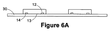
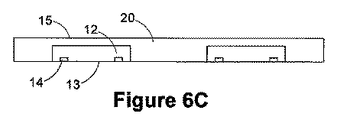
図6A乃至図6Hは、ここで開示されるデバイスの一実例となる形成方法を描写する。図6Aでは、複数の既知の良好な集積回路ダイ12は、実例となる犠牲構造30の上方に前側13を下にして置かれている。一実例では、犠牲構造30は、フィルムフレームであり、フィルムフレームは、そのフィルムフレーム全域に位置付けられたダイシングテープを有してもよい。その構造30は、後で取り除かれる点で犠牲的である。図6Bでは、例えば、モールド化合物である封入材料のボディ20は、集積回路ダイ12の周囲及び構造30の上方に形成される。つまり、集積回路ダイ12は、ボディ20に埋め込まれる。例えば、射出成形である従来のモールディング技術が、封入材料のボディ20を形成するために行われてもよい。その後、図6Cに示されるように、犠牲構造30を取り除くことができる。ここで記載される実例では、構造30は、その構造30の一部として接着テープを使用することによって、単純に剥がされてもよい。
6A-6H depict an exemplary method of forming the devices disclosed herein. In FIG. 6A, a plurality of known good integrated circuit dies 12 are placed above the illustrative
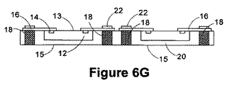
次に、図6Dに示されるように、導電性ライン16が、従来技術に従って、集積回路ダイ12の前側13及びボディ12の上方に形成される。当然に、導電性ライン16は、任意の所望の構成を有してもよく、任意の所望の材料から作られてもよい。その後、図6Eに示されるように、複数の開口またはビア17が、図のようにボディ20を貫いて形成される。開口17は、多様な既知の技術、例えば、レーザ掘削やエッチングなどによって、形成されてもよい。ある用途では、マスキング層(図示せず)が、開口17を形成するプロセスの一部として、形成されてもよい。開口17は、任意の所望の輪郭または構成を呈してもよい。ここで留意すべきは、ここで描写される実例では、開口17は、埋め込みダイ10のボディ20の後側15から前側13に向かって、形成されることである。また、この特定の例では、開口17は、埋め込みダイ10の前側13上に形成された導電性インターコネクション16を露出しているが、貫いて伸びてはいないことも留意すべきである。その後、図6Fに示されるように、開口17は、導電性インターコネクション18を形成するために、例えば、銅、アルミニウム、銀など、導電性材料で満たされる。導電性材料は、任意の多様な既知の技術、例えば、めっき、蒸着などを使用して、開口17内に形成されてもよい。また、その特定の用途に応じて、多様な異なる導電性材料が採用されてもよい。
Next, as shown in FIG. 6D,
図6Gでは、複数の導電性構造22が、既知の技術を使用して、埋め込みダイ10A及び10B上に形成される。ある場合には、導電性構造22は、導電性インターコネクション18を形成するプロセスの一部として、形成されてもよい。その後、図6Hに示されるように、ダイシングまたは単一化プロセスがカット線37に沿って実行され、実例となる個別の埋め込みダイ10A及び10Bが製造される。
In FIG. 6G, a plurality of
次に、個別の埋め込みダイ10A及び10Bは、多様なテストが行われ、意図される用途へのそれらの適合性が確認される。埋め込みダイ10A及び10Bがそのようなテストに首尾よく合格すると、それらは消費者に出荷される状態になる。他の用途では、テストされた埋め込みダイ10A及び10Bは、ここで描写されるように、積層されパッケージ化されたデバイス300、400、500にアセンブリ化されてもよい。図3で描写された例では、複数の個別の埋め込みダイ10は、図3に描写されるように位置付けられ、リフロープロセスが実行されて、個別の埋め込みダイ、例えば、ダイ10A上の導電性構造22と、隣接する埋め込みダイ、例えば、ダイ10B上の導電性インターコネクション18との間に電気的な接続が確立される。実例となる半田ボール24は、従来技術を使用して、実例となるダイ10上に形成されてもよい。半田ボール24は、リフロープロセス中の任意の時点で形成されてもよい。例えば、半田ボール24は、埋め込みダイ10A乃至10Dのすべてが図3に描写されるようにアセンブリ化された後に、形成されてもよい。あるいは、半田ボール24は、図3に描写されるように、他の個別の埋め込みダイとともに個別の埋め込みダイ10Dをアセンブリ化する前に、個別の埋め込みダイ10Dの上方に形成されてもよい。
The individual embedded dies 10A and 10B are then subjected to a variety of tests to confirm their suitability for the intended application. If embedded dies 10A and 10B successfully pass such a test, they are ready to be shipped to the consumer. In other applications, the tested embedded dies 10A and 10B may be assembled into stacked and packaged
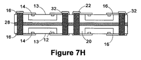
図7A乃至図7Iは、ここで開示されるデバイスの別の実例となる形成方法を描写する。図7A乃至図7Dで描写される工程は、図6A乃至図6Dに関して前述された工程と同じである。従って、図7A乃至図7Dの詳細な解説は繰り返さない。図7Eでは、図7Dで描写される複数の構造が、接着材料28を使用して互いに固定される。その後、図7Fで、図7Eに描写される組み合わせ構造のボディ20を貫いて、複数の開口またはビア31が形成される。開口31は、多様な既知の技術、例えば、レーザ掘削やエッチングなどによって、形成されてもよい。ある用途では、マスキング層(図示せず)が、開口31を形成するプロセスの一部として、形成されてもよい。開口31は、任意の所望の輪郭または構成であってもよい。ここで留意すべきは、ここで描写される実例では、開口31は、個別の構造の各々の前側13上に形成された導電性インターコネクション16を貫いて伸びることである。その後、図7Gに示されるように、開口31は、スルーボディ導電性ビア32を形成するために、例えば、銅、アルミニウム、銀などの、導電性材料で満たされる。導電性材料は、任意の多様な既知の技術、例えば、めっき、蒸着などを使用して、開口31内に形成されてもよく、また、その特定の用途に応じて、多様な異なる導電性材料が採用されてもよい。
7A-7I depict another illustrative method of forming the devices disclosed herein. The steps depicted in FIGS. 7A-7D are the same as those described above with respect to FIGS. 6A-6D. Therefore, the detailed description of FIGS. 7A to 7D will not be repeated. In FIG. 7E, the structures depicted in FIG. 7D are secured together using an
図7Hでは、複数の導電性構造22が、既知の技術を使用して、図7Gに描写される構造上に形成される。ある場合には、導電性構造22は、導電性インターコネクション32を形成するプロセスの一部として、形成されてもよい。次に、図7Iに示されるように、ダイシングまたは単一化プロセスがカット線37に沿って実行されて、実例となる個別の埋め込みのグループ10E及び10Fが製造される。
In FIG. 7H, a plurality of
次に、埋め込みダイのグループ10E及び10Fは、多様なテストが行われて、意図される用途へのそれらの適合性が確認される。グループ10E及び10Fがそのようなテストに首尾よく合格すると、それらは消費者に出荷される状態になる。ある用途では、埋め込みダイのグループ10E及び10Fは、ここで記載されるように、積層されパッケージ化されたデバイスにアセンブリ化されてもよい。図4で描写された例では、埋め込みダイのグループ10E及び10Fは、図4に描写されるように位置付けられ、リフロープロセスが実行されて、第1のグループ10E上の導電性構造22と、隣接するグループ10F上の導電性ビア32との間に電気的な接続が確立される。実例となる半田ボール24は、従来技術を使用して、グループ10F内の実例となる個別の埋め込みダイ上に形成されてもよい。半田ボール24は、リフロープロセス中の任意の時点で形成されてもよい。例えば、半田ボール24は、2つの実例となるグループ10E及び10Fが図4に描写されるようにアセンブリ化された後に、形成されてもよい。あるいは、半田ボール24は、図4に描写されるように、2つのグループを一緒にアセンブリ化する前に、グループ10F内の個別の埋め込みダイの一つの上方に形成されてもよい。
Next, the embedded
本出願を読み終えた後で当業者によって認識されるように、本開示は、個別のダイをパッケージ化し、且つ、積層されパッケージ化された集積回路デバイスを提供する、非常に効果的な手段を提供し得る。ここで実行されるプロセスの多くは、一度に個々のダイ一つでそのような動作が実行されるのとは対照的に、一度に複数のダイで実行されうる。例えば、2つの実例となるダイ12は、図6A乃至図6H及び図7A乃至図7Iで描写されるが、ここで記載されたプロセス工程は、採用されるプロセスツールのプロセス性能に応じて、任意の所望の数のダイで実行されてもよい。要するに、ウェハーレベルプロセス技術が、パッケージ化動作の効率を向上させるために採用されてもよく、つまり、プロセス動作は、同時に複数のダイで実行されうる。 As will be appreciated by those skilled in the art after reading this application, this disclosure provides a highly effective means of packaging individual dies and providing stacked and packaged integrated circuit devices. Can be provided. Many of the processes performed here can be performed on multiple dies at once, as opposed to performing such operations on one individual die at a time. For example, two illustrative dies 12 are depicted in FIGS. 6A-6H and FIGS. 7A-7I, but the process steps described herein are optional depending on the process performance of the process tool employed. May be performed with any desired number of dies. In short, wafer level process technology may be employed to improve the efficiency of packaging operations, that is, process operations can be performed on multiple dies simultaneously.
Claims (16)
アクティブ面と前記アクティブ面の反対側の裏面とを有する第1の半導体ダイと、
前記第1の半導体ダイを封入する第1の封入材であって、前記第1の封入材は前面と前記前面と反対側の裏面とを有し、前記第1の半導体ダイの前記アクティブ面は概して前記第1の封入材の前記前面と同一平面にあり、前記第1の半導体ダイの前記裏面は前記第1の封入材に埋め込まれる、という第1の封入材と、
前記第1の封入材の前記前面上に配置されて且つ前記第1の半導体ダイの前記アクティブ面と概して同一平面にある第1の導電性ラインと、
アクティブ面と前記アクティブ面の反対側の裏面とを有する第2の半導体ダイと、
前記第2の半導体ダイを封入する第2の封入材であって、前記第2の封入材は前面と前記前面と反対側の裏面とを有し、前記第2の半導体ダイの前記アクティブ面は概して前記第2の封入材の前記前面と同一平面にあり、前記第2の半導体ダイの前記裏面は前記第2の封入材に埋め込まれる、という第2の封入材と、
前記第2の封入材の前記前面上に配置されて且つ前記第2の半導体ダイの前記アクティブ面と概して同一平面にある第2の導電性ラインであって、前記第1の封入材の前記裏面が前記第2の封入材の前記裏面を向く、という第2の導電性ラインと、
前記第1の封入材の前記前面から前記第2の封入材の前記前面まで、前記第1の封入材及び前記第2の封入材を貫通して伸びる導電性ビアであって、前記導電性ビアは、前記第1の封入材の前記前面で前記第1の導電性ラインと直接接触し、前記第2の封入材の前記前面で前記第2の導電性ラインと直接接触する、という導電性ビアと、を含む
ことを特徴とする半導体デバイス。 A semiconductor device,
A first semiconductor die having an active surface and a back surface opposite the active surface;
First an encapsulating material encapsulating the first semiconductor die, wherein the first encapsulant and a back surface opposite to the front and front, the active surface of the first semiconductor die and generally it is in the front flush with the first encapsulant, the first of the back surface of the semiconductor die is embedded in the first encapsulant, the first encapsulant that,
A first conductive line disposed on the front surface of the first encapsulant and generally coplanar with the active surface of the first semiconductor die;
A second semiconductor die having an active surface and a back surface opposite the active surface;
A second encapsulant for encapsulating the second semiconductor die, the second encapsulant having a front surface and a back surface opposite to the front surface, wherein the active surface of the second semiconductor die is A second encapsulant that is generally flush with the front surface of the second encapsulant and wherein the back surface of the second semiconductor die is embedded in the second encapsulant;
A second conductive line disposed on the front surface of the second encapsulant and generally coplanar with the active surface of the second semiconductor die, the back surface of the first encapsulant A second conductive line that faces the back surface of the second encapsulant;
Wherein from the front surface of the first encapsulant to said front surface of said second encapsulant, a conductive via extending through the first encapsulant and the second encapsulant, the conductive A via that is in direct contact with the first conductive line at the front surface of the first encapsulant and in direct contact with the second conductive line at the front surface of the second encapsulant ; A semiconductor device comprising a via.
前記導電性ビアは、第1の導電性ビアであり、
前記半導体デバイスは、さらに、前記第1の封入材の前記前面から前記第2の封入材の前面まで、前記第1の封入材及び前記第2の封入材を貫通して伸びた第2の導電性ビアを含み、前記第2の導電性ビアは、前記第1の封入材の前記前面で前記第1の導電性ラインと直接接触し、前記第2の封入材の前記前面で前記第2の導電性ラインと直接接触し、
前記第2の導電性ビアは、前記第1の半導体ダイと前記第2の半導体ダイから、及び、前記第1の導電性ビアから、横方向に間隔を空けて離れていて、
前記半導体デバイスは、さらに、前記第1の導電性ラインに取付けられた第1の半田ボールと、前記第2の導電性ラインに取付けられた第2の半田ボールとを含む
ことを特徴とする半導体デバイス。 The semiconductor device according to claim 1,
Before Kishirubedensei via is a first conductive via,
The semiconductor device further from the front face of the first encapsulant to the front of the second encapsulant, the second extending through said first encapsulant and the second encapsulant A conductive via, wherein the second conductive via is in direct contact with the first conductive line at the front of the first encapsulant and the second at the front of the second encapsulant . In direct contact with the conductive line of
Said second conductive vias, wherein the first semiconductor die and the second semiconductor die, and the first conductive vias or al, have laterally spaced at intervals,
The semiconductor device further includes a first solder ball attached to the first conductive line and a second solder ball attached to the second conductive line. device.
前記導電性ビアは、前記第1の半導体ダイから、横方向に間隔を空けて離れている
ことを特徴とする半導体デバイス。 The semiconductor device according to claim 1,
The semiconductor device, wherein the conductive via is spaced laterally from the first semiconductor die.
前記導電性ビアは、第1の導電性ビアであり、
前記半導体デバイスは、さらに、前記第1の封入材の前記前面から前記第2の封入材の前記前面まで、前記第1の封入材及び前記第2の封入材を貫通して伸びた第2の導電性ビアを含み、前記第2の導電性ビアは、前記第1の半導体ダイ及び前記第1の導電性ビアから、横方向に間隔を空けて離れている
ことを特徴とする半導体デバイス。 The semiconductor device according to claim 1,
The conductive via is a first conductive via;
The semiconductor device further from the front face of the first encapsulant to said front surface of said second encapsulant, the second extending through said first encapsulant and the second encapsulant of include a conductive via, said second conductive vias, semiconductor devices, characterized in that from the first semiconductor die and the first conductive via, spaced laterally at intervals.
前記第1の半導体ダイは、さらに、前記第1の半導体ダイの前記アクティブ面に、第1のボンドパッドと第3のボンドパッドとを含み、
前記第1のボンドパッドは、前記第1の導電性ラインと接触し、
前記半導体デバイスは、さらに、前記第1の半導体ダイの前記アクティブ面に、前記第3のボンドパッドと接触する第3の導電性ラインを含み、
前記導電性ビアは、第1の導電性ビアであり、
前記半導体デバイスは、さらに、前記第1の封入材の前記前面から前記第2の封入材の前記前面まで伸びた第2の導電性ビアを含み、前記第2の導電性ビアは、前記第3の導電性ラインと直接接触している
ことを特徴とする半導体デバイス。 The semiconductor device according to claim 1,
Before SL first semiconductor die, further to the active surface of the first semiconductor die comprises a first bond pad and a third bond pad,
The first bond pad is in contact with the first conductive line;
The semiconductor device further on the active surface of the first semiconductor die comprises a third conductive line contacting the third bond pad,
The conductive via is a first conductive via;
The semiconductor device further comprises a second conductive via extending from the front surface of the first encapsulant to said front surface of said second encapsulant, said second conductive via, said first 3. A semiconductor device characterized in that it is in direct contact with the three conductive lines.
前記第1の導電性ラインと第2の導電性ラインそれぞれに取付けられた第1の半田ボールと第2の半田ボールを含む
ことを特徴とする半導体デバイス。 The semiconductor device of claim 1, further comprising:
Semiconductor devices, characterized in that it comprises a first solder ball and the second solder balls attached to each of the first conductive lines and second conductive lines.
第1の半導体サブアセンブリと、
前記第1の半導体サブアセンブリに最も近い第2の半導体サブアセンブリであって、前記第1及び前記第2の半導体サブアセンブリが各々前側と後側を有し、その上、前記第1の半導体サブアセンブリの前記後側が前記第2の半導体サブアセンブリの前記後側と向かい合う、という第2の半導体サブアセンブリと、を含み、
前記第1及び前記第2の半導体サブアセンブリが個々に、
封入材と、
前記封入材に埋め込まれた半導体ダイであって、前記半導体ダイは、概して前記第1または前記第2の半導体サブアセンブリの前記前側と同一平面にあるアクティブ面と、前記封入材に埋め込まれた裏面とを有する、という半導体ダイと、
前記個々の第1及び第2の半導体サブアセンブリの前記前側上に配置されて且つ前記半導体ダイの前記アクティブ面と概して同一平面にある導電性ラインと、
前記第1の半導体サブアセンブリの前記前側から前記第2の半導体サブアセンブリの前記前側まで、前記第1及び前記第2の半導体サブアセンブリを貫通して伸びる導電性ビアであって、前記導電性ビアが前記第1の半導体サブアセンブリの前記導電性ライン及び第2の半導体サブアセンブリの前記導電性ラインと直接接触する、という導電性ビアと、を有する
ことを特徴とする半導体デバイス。 A semiconductor device,
A first semiconductor subassembly;
A second semiconductor subassembly closest to the first semiconductor subassembly, wherein the first and second semiconductor subassemblies each have a front side and a rear side; A second semiconductor subassembly, wherein the rear side of the assembly faces the rear side of the second semiconductor subassembly;
The first and second semiconductor subassemblies individually;
An encapsulant;
A semiconductor die embedded in the encapsulant, wherein the semiconductor die is generally an active surface that is coplanar with the front side of the first or second semiconductor subassembly, and a back surface embedded in the encapsulant A semiconductor die having
A conductive line disposed on the front side of the individual first and second semiconductor subassemblies and generally coplanar with the active surface of the semiconductor die;
A conductive via extending through the first and second semiconductor subassemblies from the front side of the first semiconductor subassembly to the front side of the second semiconductor subassembly , the conductive via; There semiconductor device according to claim Rukoto to have a, a conductive via that contacts the conductive line and direct the conductive lines and the second semiconductor sub-assembly of the first semiconductor subassembly.
前記半導体デバイスは、さらに、前記第1の半導体サブアセンブリの前記導電性ラインに取付けられた半田ボールを含む
ことを特徴とする半導体デバイス。 The semiconductor device according to claim 7 .
Before Symbol semiconductor device further semiconductor device which comprises a solder ball attached to the conductive lines of the first semiconductor subassembly.
前記導電性ビアは、第1の導電性ビアであり、
前記半導体デバイスは、さらに、
前記第1の半導体サブアセンブリの前記前側から前記第2の半導体サブアセンブリの前記前側まで、前記第1及び前記第2の半導体サブアセンブリを貫通して伸びる第2の導電性ビアであって、前記第1の半導体サブアセンブリの前記半導体ダイと前記第2の半導体サブアセンブリの前記半導体ダイから、及び、前記第1の導電性ビアから横方向に間隔を空けて離れているという第2の導電性ビアを含む
ことを特徴とする半導体デバイス。 The semiconductor device according to claim 7 .
The conductive via is a first conductive via;
The semiconductor device further includes:
A second conductive via extending through the first and second semiconductor subassemblies from the front side of the first semiconductor subassembly to the front side of the second semiconductor subassembly; Second conductivity that is laterally spaced from the semiconductor die of the first semiconductor subassembly and the semiconductor die of the second semiconductor subassembly and from the first conductive via. A semiconductor device comprising a via .
前記第1の半導体サブアセンブリの前記後側と前記第2の半導体サブアセンブリの前記後側との間に接着材を含む
ことを特徴とする半導体デバイス。 The semiconductor device according to claim 7 , further comprising:
A semiconductor device , comprising an adhesive between the back side of the first semiconductor subassembly and the back side of the second semiconductor subassembly .
前記第1及び前記第2の半導体サブアセンブリの各々は、複数の集積回路ダイを含む
ことを特徴とする半導体デバイス。 The semiconductor device according to claim 7 .
Each of the first and second semiconductor subassemblies includes a plurality of integrated circuit dies.
第1の半導体ダイを封入材で前側と後側を有する第1の半導体構造に封入する工程であって、前記第1の半導体ダイは、概して前記前側と同一平面にあるアクティブ面と、前記封入材に埋め込まれた裏面とを有する、という工程と、
前記第1の半導体構造の前記前側に第1の導電性ラインを形成する工程であって、前記第1の導電性ラインが前記第1の半導体ダイの前記アクティブ面と概して同一平面にあるという工程と、
第2の半導体ダイを封入材で前側と後側を有する第2の半導体構造に封入する工程であって、前記第2の半導体ダイは、概して前記前側と同一平面にあるアクティブ面と、前記封入材に埋め込まれた裏面とを有する、という工程と、
前記第2の半導体構造の前記前側に第2の導電性ラインを形成する工程であって、前記第2の導電性ラインが前記第2の半導体ダイの前記アクティブ面と概して同一平面にあるという工程と、
前記第1の半導体構造の前記前側から前記第2の半導体構造の前記前側まで前記第1の半導体構造及び前記第2の半導体構造を貫通して伸びた導電性ビアを形成する工程であって、前記導電性ビアが前記第1の半導体構造の前記第1の導電性ライン及び前記第2の半導体構造の前記第2の導電性ラインと直接接触する、という工程と、を含む
ことを特徴とする方法。 A method for manufacturing a semiconductor device, comprising:
Encapsulating a first semiconductor die with an encapsulant in a first semiconductor structure having a front side and a rear side, the first semiconductor die comprising an active surface generally coplanar with the front side; and the encapsulation Having a back surface embedded in the material;
Step of the said front side of the first semiconductor structure comprising: forming a first conductive line, the first conductive lines are in generally coplanar with the active surface of the first semiconductor die When,
Encapsulating a second semiconductor die with an encapsulant in a second semiconductor structure having a front side and a rear side, wherein the second semiconductor die is generally an active surface coplanar with the front side; and the encapsulation Having a back surface embedded in the material;
Forming a second conductive line on the front side of the second semiconductor structure, wherein the second conductive line is generally flush with the active surface of the second semiconductor die. When,
And forming said first of said second of said first semiconductor structure and the second conductive vias extending through the semiconductor structure before the side of the semiconductor structure from the front side of the semiconductor structure And wherein the conductive via directly contacts the first conductive line of the first semiconductor structure and the second conductive line of the second semiconductor structure. how to.
前記第1の半導体ダイを封入する工程は、
前記第1の半導体ダイを犠牲構造に配置する工程であって、前記第1の半導体ダイの前記アクティブ面が前記犠牲構造に接触する、という工程と、
前記犠牲構造に配置された前記第1の半導体ダイを封入する工程と、
前記犠牲構造を取り除く工程と、
前記第1の半導体ダイの前記アクティブ面を露出する工程と、を含む
ことを特徴とする方法。 The method of claim 12 , wherein
Encapsulating the first semiconductor die comprises:
Placing the first semiconductor die in a sacrificial structure, wherein the active surface of the first semiconductor die contacts the sacrificial structure;
Encapsulating the first semiconductor die disposed in the sacrificial structure;
Removing the sacrificial structure;
Exposing the active surface of the first semiconductor die.
前記第2の半導体ダイを封入する工程は、
複数の第2の半導体ダイを前記封入材で封入する工程と、
前記封入された第2の半導体ダイを単一化する工程と、を含む
ことを特徴とする方法。 The method of claim 12 , wherein
The step of encapsulating the second semiconductor die includes:
Encapsulating a plurality of second semiconductor dies with the encapsulant;
Singulating the encapsulated second semiconductor die.
前記方法は、さらに、前記第1の半導体ダイと前記第2の半導体ダイを犠牲構造上に配置する工程を含み、
前記第1及び前記第2の半導体ダイを封入する工程は、
前記第1及び前記第2の半導体ダイの両方を前記封入材で封入しながら、前記第1及び前記第2の半導体ダイが前記犠牲構造上に置かれる、という工程と、
その後に、
前記第1及び前記第2の半導体ダイから前記犠牲構造を取り除く工程と、
前記封入された第1及び前記第2の半導体ダイを単一化する工程と、を含む
ことを特徴とする方法。 The method of claim 12 , wherein
Before SL method further comprises the step of placing the said first semiconductor die and the second semiconductor die on the sacrificial structure,
Encapsulating the first and second semiconductor dies includes:
Placing the first and second semiconductor dies on the sacrificial structure while encapsulating both the first and second semiconductor dies with the encapsulant;
Then
Removing the sacrificial structure from the first and second semiconductor dies;
Singulating the encapsulated first and second semiconductor dies.
前記方法は、さらに、前記第1の半導体ダイ及び前記第2の半導体ダイを犠牲構造上に配置する工程を含み、
前記第1及び前記第2の半導体ダイを封入する工程は、
前記第1及び前記第2の半導体ダイの両方を前記封入材で封入しながら、前記第1及び前記第2の半導体ダイが前記犠牲構造上に置かれる、という工程と、
その後に、
前記第1及び前記第2の半導体ダイから前記犠牲構造を取り除く工程と、
前記封入された第1及び第2の半導体ダイを単一化して、前記第1の半導体構造及び前記第2の半導体構造を形成する工程と、
前記第1及び前記第2の半導体構造の間に接着剤を配置する工程と、を含む
ことを特徴とする方法。 The method of claim 12 , wherein
Before SL method further comprises a step of placing the first semiconductor die and the second semiconductor die on the sacrificial structure,
Encapsulating the first and second semiconductor dies includes:
Placing the first and second semiconductor dies on the sacrificial structure while encapsulating both the first and second semiconductor dies with the encapsulant;
Then
Removing the sacrificial structure from the first and second semiconductor dies;
A step of singulated first and second semiconductor dies said enclosed, forming the first semiconductor structure and said second semiconductor structure,
Disposing an adhesive between the first and second semiconductor structures .
Applications Claiming Priority (3)
| Application Number | Priority Date | Filing Date | Title |
|---|---|---|---|
| US11/834,765 US7781877B2 (en) | 2007-08-07 | 2007-08-07 | Packaged integrated circuit devices with through-body conductive vias, and methods of making same |
| US11/834,765 | 2007-08-07 | ||
| PCT/US2008/071994 WO2009045626A1 (en) | 2007-08-07 | 2008-08-01 | Packaged integrated circuit devices with through- body conductive vias, and methods of making same |
Publications (3)
| Publication Number | Publication Date |
|---|---|
| JP2010536178A JP2010536178A (en) | 2010-11-25 |
| JP2010536178A5 JP2010536178A5 (en) | 2011-09-22 |
| JP5723153B2 true JP5723153B2 (en) | 2015-05-27 |
Family
ID=40012850
Family Applications (1)
| Application Number | Title | Priority Date | Filing Date |
|---|---|---|---|
| JP2010520232A Active JP5723153B2 (en) | 2007-08-07 | 2008-08-01 | Packaged integrated circuit device with through-body conductive vias and method of manufacturing the same |
Country Status (7)
| Country | Link |
|---|---|
| US (7) | US7781877B2 (en) |
| EP (2) | EP2186135A1 (en) |
| JP (1) | JP5723153B2 (en) |
| KR (1) | KR101722264B1 (en) |
| CN (1) | CN101772841B (en) |
| TW (1) | TWI437683B (en) |
| WO (1) | WO2009045626A1 (en) |
Families Citing this family (124)
| Publication number | Priority date | Publication date | Assignee | Title |
|---|---|---|---|---|
| US8525314B2 (en) | 2004-11-03 | 2013-09-03 | Tessera, Inc. | Stacked packaging improvements |
| US8058101B2 (en) | 2005-12-23 | 2011-11-15 | Tessera, Inc. | Microelectronic packages and methods therefor |
| US7781877B2 (en) * | 2007-08-07 | 2010-08-24 | Micron Technology, Inc. | Packaged integrated circuit devices with through-body conductive vias, and methods of making same |
| US8044497B2 (en) * | 2007-09-10 | 2011-10-25 | Intel Corporation | Stacked die package |
| US7863755B2 (en) * | 2008-03-19 | 2011-01-04 | Stats Chippac Ltd. | Package-on-package system with via Z-interconnections |
| SG142321A1 (en) * | 2008-04-24 | 2009-11-26 | Micron Technology Inc | Pre-encapsulated cavity interposer |
| US8130527B2 (en) * | 2008-09-11 | 2012-03-06 | Micron Technology, Inc. | Stacked device identification assignment |
| US20100133682A1 (en) | 2008-12-02 | 2010-06-03 | Infineon Technologies Ag | Semiconductor device |
| US8258010B2 (en) * | 2009-03-17 | 2012-09-04 | Stats Chippac, Ltd. | Making a semiconductor device having conductive through organic vias |
| JP5215244B2 (en) * | 2009-06-18 | 2013-06-19 | 新光電気工業株式会社 | Semiconductor device |
| US8310835B2 (en) * | 2009-07-14 | 2012-11-13 | Apple Inc. | Systems and methods for providing vias through a modular component |
| TWI405306B (en) | 2009-07-23 | 2013-08-11 | Advanced Semiconductor Eng | Semiconductor package, manufacturing method thereof and chip-redistribution encapsulant |
| US8367470B2 (en) * | 2009-08-07 | 2013-02-05 | Stats Chippac, Ltd. | Semiconductor device and method of forming cavity in build-up interconnect structure for short signal path between die |
| KR101088822B1 (en) * | 2009-08-10 | 2011-12-01 | 주식회사 하이닉스반도체 | Semiconductor package |
| US7923304B2 (en) * | 2009-09-10 | 2011-04-12 | Stats Chippac Ltd. | Integrated circuit packaging system with conductive pillars and method of manufacture thereof |
| KR101563630B1 (en) * | 2009-09-17 | 2015-10-28 | 에스케이하이닉스 주식회사 | Semiconductor package |
| US20110084372A1 (en) | 2009-10-14 | 2011-04-14 | Advanced Semiconductor Engineering, Inc. | Package carrier, semiconductor package, and process for fabricating same |
| US8378466B2 (en) | 2009-11-19 | 2013-02-19 | Advanced Semiconductor Engineering, Inc. | Wafer-level semiconductor device packages with electromagnetic interference shielding |
| TWI408785B (en) | 2009-12-31 | 2013-09-11 | Advanced Semiconductor Eng | Semiconductor package |
| US8569894B2 (en) | 2010-01-13 | 2013-10-29 | Advanced Semiconductor Engineering, Inc. | Semiconductor package with single sided substrate design and manufacturing methods thereof |
| US8372689B2 (en) | 2010-01-21 | 2013-02-12 | Advanced Semiconductor Engineering, Inc. | Wafer-level semiconductor device packages with three-dimensional fan-out and manufacturing methods thereof |
| US8138014B2 (en) | 2010-01-29 | 2012-03-20 | Stats Chippac, Ltd. | Method of forming thin profile WLCSP with vertical interconnect over package footprint |
| US8320134B2 (en) | 2010-02-05 | 2012-11-27 | Advanced Semiconductor Engineering, Inc. | Embedded component substrate and manufacturing methods thereof |
| TWI419283B (en) | 2010-02-10 | 2013-12-11 | Advanced Semiconductor Eng | Package structure |
| TWI411075B (en) | 2010-03-22 | 2013-10-01 | Advanced Semiconductor Eng | Semiconductor package and manufacturing method thereof |
| US8698322B2 (en) * | 2010-03-24 | 2014-04-15 | Oracle International Corporation | Adhesive-bonded substrates in a multi-chip module |
| US8278746B2 (en) * | 2010-04-02 | 2012-10-02 | Advanced Semiconductor Engineering, Inc. | Semiconductor device packages including connecting elements |
| US8624374B2 (en) | 2010-04-02 | 2014-01-07 | Advanced Semiconductor Engineering, Inc. | Semiconductor device packages with fan-out and with connecting elements for stacking and manufacturing methods thereof |
| US8677613B2 (en) | 2010-05-20 | 2014-03-25 | International Business Machines Corporation | Enhanced modularity in heterogeneous 3D stacks |
| US10672748B1 (en) * | 2010-06-02 | 2020-06-02 | Maxim Integrated Products, Inc. | Use of device assembly for a generalization of three-dimensional heterogeneous technologies integration |
| US8482111B2 (en) | 2010-07-19 | 2013-07-09 | Tessera, Inc. | Stackable molded microelectronic packages |
| US9159708B2 (en) | 2010-07-19 | 2015-10-13 | Tessera, Inc. | Stackable molded microelectronic packages with area array unit connectors |
| DE102010041129A1 (en) | 2010-09-21 | 2012-03-22 | Robert Bosch Gmbh | Multifunction sensor as PoP mWLP |
| TWI451546B (en) | 2010-10-29 | 2014-09-01 | Advanced Semiconductor Eng | Stacked semiconductor package, semiconductor package thereof and method for making a semiconductor package |
| US8941222B2 (en) | 2010-11-11 | 2015-01-27 | Advanced Semiconductor Engineering Inc. | Wafer level semiconductor package and manufacturing methods thereof |
| KR101075241B1 (en) | 2010-11-15 | 2011-11-01 | 테세라, 인코포레이티드 | Microelectronic package with terminals on dielectric mass |
| US8343808B2 (en) | 2010-11-22 | 2013-01-01 | Bridge Semiconductor Corporation | Method of making stackable semiconductor assembly with bump/base/flange heat spreader and build-up circuitry |
| US8841171B2 (en) | 2010-11-22 | 2014-09-23 | Bridge Semiconductor Corporation | Method of making stackable semiconductor assembly with bump/flange heat spreader and dual build-up circuitry |
| US20120126399A1 (en) | 2010-11-22 | 2012-05-24 | Bridge Semiconductor Corporation | Thermally enhanced semiconductor assembly with bump/base/flange heat spreader and build-up circuitry |
| US20120146206A1 (en) | 2010-12-13 | 2012-06-14 | Tessera Research Llc | Pin attachment |
| US9406658B2 (en) | 2010-12-17 | 2016-08-02 | Advanced Semiconductor Engineering, Inc. | Embedded component device and manufacturing methods thereof |
| US9171792B2 (en) | 2011-02-28 | 2015-10-27 | Advanced Semiconductor Engineering, Inc. | Semiconductor device packages having a side-by-side device arrangement and stacking functionality |
| WO2012126374A1 (en) | 2011-03-22 | 2012-09-27 | Nantong Fujitsu Microelectronics Co., Ltd. | 3d system-level packaging methods and structures |
| WO2012126377A1 (en) | 2011-03-22 | 2012-09-27 | Nantong Fujitsu Microelectronics Co., Ltd. | System-level packaging methods and structures |
| US8618659B2 (en) | 2011-05-03 | 2013-12-31 | Tessera, Inc. | Package-on-package assembly with wire bonds to encapsulation surface |
| KR101128063B1 (en) | 2011-05-03 | 2012-04-23 | 테세라, 인코포레이티드 | Package-on-package assembly with wire bonds to encapsulation surface |
| US8389333B2 (en) * | 2011-05-26 | 2013-03-05 | Stats Chippac, Ltd. | Semiconductor device and method of forming EWLB package containing stacked semiconductor die electrically connected through conductive vias formed in encapsulant around die |
| US8653639B2 (en) * | 2011-06-09 | 2014-02-18 | Headway Technologies, Inc. | Layered chip package and method of manufacturing same |
| US9324659B2 (en) * | 2011-08-01 | 2016-04-26 | Stats Chippac, Ltd. | Semiconductor device and method of forming POP with stacked semiconductor die and bumps formed directly on the lower die |
| CN103718292A (en) * | 2011-08-11 | 2014-04-09 | 弗利普芯片国际有限公司 | Thin film structure for high density inductors and redistribution in wafer level packaging |
| US8765497B2 (en) * | 2011-09-02 | 2014-07-01 | Taiwan Semiconductor Manufacturing Company, Ltd. | Packaging and function tests for package-on-package and system-in-package structures |
| US9123763B2 (en) | 2011-10-12 | 2015-09-01 | Taiwan Semiconductor Manufacturing Company, Ltd. | Package-on-package (PoP) structure having at least one package comprising one die being disposed in a core material between first and second surfaces of the core material |
| US8404520B1 (en) | 2011-10-17 | 2013-03-26 | Invensas Corporation | Package-on-package assembly with wire bond vias |
| US8975741B2 (en) | 2011-10-17 | 2015-03-10 | Taiwan Semiconductor Manufacturing Company, Ltd. | Process for forming package-on-package structures |
| US11445617B2 (en) * | 2011-10-31 | 2022-09-13 | Unimicron Technology Corp. | Package structure and manufacturing method thereof |
| US20170374748A1 (en) | 2011-10-31 | 2017-12-28 | Unimicron Technology Corp. | Package structure and manufacturing method thereof |
| US8623711B2 (en) * | 2011-12-15 | 2014-01-07 | Stats Chippac Ltd. | Integrated circuit packaging system with package-on-package and method of manufacture thereof |
| US8629567B2 (en) | 2011-12-15 | 2014-01-14 | Stats Chippac Ltd. | Integrated circuit packaging system with contacts and method of manufacture thereof |
| US9219029B2 (en) | 2011-12-15 | 2015-12-22 | Stats Chippac Ltd. | Integrated circuit packaging system with terminals and method of manufacture thereof |
| US8946757B2 (en) | 2012-02-17 | 2015-02-03 | Invensas Corporation | Heat spreading substrate with embedded interconnects |
| US9349706B2 (en) | 2012-02-24 | 2016-05-24 | Invensas Corporation | Method for package-on-package assembly with wire bonds to encapsulation surface |
| US8372741B1 (en) | 2012-02-24 | 2013-02-12 | Invensas Corporation | Method for package-on-package assembly with wire bonds to encapsulation surface |
| KR20130123720A (en) * | 2012-05-03 | 2013-11-13 | 에스케이하이닉스 주식회사 | Semicondcutor chip, semiconductor package having the same, and stacked semiconductor package using the semiconductor package |
| US8835228B2 (en) | 2012-05-22 | 2014-09-16 | Invensas Corporation | Substrate-less stackable package with wire-bond interconnect |
| US9391008B2 (en) * | 2012-07-31 | 2016-07-12 | Invensas Corporation | Reconstituted wafer-level package DRAM |
| US9502390B2 (en) | 2012-08-03 | 2016-11-22 | Invensas Corporation | BVA interposer |
| TWI497645B (en) * | 2012-08-03 | 2015-08-21 | 矽品精密工業股份有限公司 | Semiconductor package and method for forming the same |
| US8987851B2 (en) * | 2012-09-07 | 2015-03-24 | Mediatek Inc. | Radio-frequency device package and method for fabricating the same |
| KR101999262B1 (en) * | 2012-09-12 | 2019-07-12 | 삼성전자주식회사 | Semiconductor Package and method for fabricating the same |
| US8975738B2 (en) | 2012-11-12 | 2015-03-10 | Invensas Corporation | Structure for microelectronic packaging with terminals on dielectric mass |
| US8878353B2 (en) | 2012-12-20 | 2014-11-04 | Invensas Corporation | Structure for microelectronic packaging with bond elements to encapsulation surface |
| US9136254B2 (en) | 2013-02-01 | 2015-09-15 | Invensas Corporation | Microelectronic package having wire bond vias and stiffening layer |
| KR20140111523A (en) * | 2013-03-11 | 2014-09-19 | 삼성전자주식회사 | Semiconductor package and method for fabricating the same |
| EP2781230B1 (en) | 2013-03-22 | 2019-08-21 | TecPharma Licensing AG | Substance dispensing device with a signaling device |
| TWI555166B (en) * | 2013-06-18 | 2016-10-21 | 矽品精密工業股份有限公司 | Stack package and method of manufacture |
| US8941244B1 (en) * | 2013-07-03 | 2015-01-27 | Taiwan Semiconductor Manufacturing Company Ltd. | Semiconductor device and manufacturing method thereof |
| US9167710B2 (en) | 2013-08-07 | 2015-10-20 | Invensas Corporation | Embedded packaging with preformed vias |
| US9685365B2 (en) | 2013-08-08 | 2017-06-20 | Invensas Corporation | Method of forming a wire bond having a free end |
| US20150076714A1 (en) | 2013-09-16 | 2015-03-19 | Invensas Corporation | Microelectronic element with bond elements to encapsulation surface |
| CN103474361B (en) * | 2013-09-29 | 2016-06-01 | 华进半导体封装先导技术研发中心有限公司 | A kind of embedded active packaging process and encapsulation structure imbedding function substrate |
| US9583456B2 (en) | 2013-11-22 | 2017-02-28 | Invensas Corporation | Multiple bond via arrays of different wire heights on a same substrate |
| US9263394B2 (en) | 2013-11-22 | 2016-02-16 | Invensas Corporation | Multiple bond via arrays of different wire heights on a same substrate |
| US9379074B2 (en) | 2013-11-22 | 2016-06-28 | Invensas Corporation | Die stacks with one or more bond via arrays of wire bond wires and with one or more arrays of bump interconnects |
| US9583411B2 (en) | 2014-01-17 | 2017-02-28 | Invensas Corporation | Fine pitch BVA using reconstituted wafer with area array accessible for testing |
| JP6354285B2 (en) * | 2014-04-22 | 2018-07-11 | オムロン株式会社 | Resin structure in which electronic component is embedded and method for manufacturing the same |
| US10381326B2 (en) | 2014-05-28 | 2019-08-13 | Invensas Corporation | Structure and method for integrated circuits packaging with increased density |
| US9646917B2 (en) | 2014-05-29 | 2017-05-09 | Invensas Corporation | Low CTE component with wire bond interconnects |
| US9412714B2 (en) | 2014-05-30 | 2016-08-09 | Invensas Corporation | Wire bond support structure and microelectronic package including wire bonds therefrom |
| US9536753B2 (en) * | 2014-10-02 | 2017-01-03 | Texas Instruments Incorporated | Circuit substrate interconnect |
| US9735084B2 (en) | 2014-12-11 | 2017-08-15 | Invensas Corporation | Bond via array for thermal conductivity |
| US9888579B2 (en) | 2015-03-05 | 2018-02-06 | Invensas Corporation | Pressing of wire bond wire tips to provide bent-over tips |
| DE102015105692A1 (en) * | 2015-04-14 | 2016-10-20 | Osram Opto Semiconductors Gmbh | Semiconductor device and method for producing a plurality of semiconductor devices |
| US9971970B1 (en) | 2015-04-27 | 2018-05-15 | Rigetti & Co, Inc. | Microwave integrated quantum circuits with VIAS and methods for making the same |
| US9502372B1 (en) | 2015-04-30 | 2016-11-22 | Invensas Corporation | Wafer-level packaging using wire bond wires in place of a redistribution layer |
| US9761554B2 (en) | 2015-05-07 | 2017-09-12 | Invensas Corporation | Ball bonding metal wire bond wires to metal pads |
| US9741620B2 (en) * | 2015-06-24 | 2017-08-22 | Invensas Corporation | Structures and methods for reliable packages |
| US9673183B2 (en) | 2015-07-07 | 2017-06-06 | Micron Technology, Inc. | Methods of making semiconductor device packages and related semiconductor device packages |
| US9768145B2 (en) * | 2015-08-31 | 2017-09-19 | Taiwan Semiconductor Manufacturing Company, Ltd. | Methods of forming multi-die package structures including redistribution layers |
| FR3041209B1 (en) * | 2015-09-15 | 2017-09-15 | Sagem Defense Securite | COMPACT ELECTRONIC SYSTEM AND DEVICE COMPRISING SUCH A SYSTEM |
| US10490528B2 (en) | 2015-10-12 | 2019-11-26 | Invensas Corporation | Embedded wire bond wires |
| US9490222B1 (en) | 2015-10-12 | 2016-11-08 | Invensas Corporation | Wire bond wires for interference shielding |
| US10332854B2 (en) | 2015-10-23 | 2019-06-25 | Invensas Corporation | Anchoring structure of fine pitch bva |
| US10181457B2 (en) | 2015-10-26 | 2019-01-15 | Invensas Corporation | Microelectronic package for wafer-level chip scale packaging with fan-out |
| US10043779B2 (en) | 2015-11-17 | 2018-08-07 | Invensas Corporation | Packaged microelectronic device for a package-on-package device |
| US9659848B1 (en) | 2015-11-18 | 2017-05-23 | Invensas Corporation | Stiffened wires for offset BVA |
| WO2017111952A1 (en) | 2015-12-22 | 2017-06-29 | Intel Corporation | Ultra small molded module integrated with die by module-on-wafer assembly |
| US9984992B2 (en) | 2015-12-30 | 2018-05-29 | Invensas Corporation | Embedded wire bond wires for vertical integration with separate surface mount and wire bond mounting surfaces |
| US10429329B2 (en) * | 2016-01-29 | 2019-10-01 | Ams Sensors Uk Limited | Environmental sensor test methodology |
| US9935075B2 (en) | 2016-07-29 | 2018-04-03 | Invensas Corporation | Wire bonding method and apparatus for electromagnetic interference shielding |
| WO2018116799A1 (en) * | 2016-12-21 | 2018-06-28 | 株式会社村田製作所 | Method for manufacturing electronic component-incorporating substrate, electronic component-incorporating substrate, electronic component device, and communication module |
| US10299368B2 (en) | 2016-12-21 | 2019-05-21 | Invensas Corporation | Surface integrated waveguides and circuit structures therefor |
| US11121301B1 (en) | 2017-06-19 | 2021-09-14 | Rigetti & Co, Inc. | Microwave integrated quantum circuits with cap wafers and their methods of manufacture |
| US11328969B2 (en) * | 2017-11-16 | 2022-05-10 | Amkor Technology Singapore Holding Pte. Ltd. | Semiconductor device and manufacturing method thereof |
| US10510705B2 (en) * | 2017-12-29 | 2019-12-17 | Advanced Semiconductor Engineering, Inc. | Semiconductor package structure having a second encapsulant extending in a cavity defined by a first encapsulant |
| JP2019216187A (en) * | 2018-06-13 | 2019-12-19 | ソニーセミコンダクタソリューションズ株式会社 | Imaging apparatus |
| CN108962772B (en) * | 2018-07-19 | 2021-01-22 | 通富微电子股份有限公司 | Package structure and method for forming the same |
| US11251100B2 (en) * | 2019-09-25 | 2022-02-15 | Taiwan Semiconductor Manufacturing Company, Ltd. | Semiconductor structure having an anti-arcing pattern disposed on a passivation layer and method of fabricating the semiconductor structure |
| IT201900024292A1 (en) | 2019-12-17 | 2021-06-17 | St Microelectronics Srl | PROCEDURE FOR MANUFACTURING SEMICONDUCTOR DEVICES AND CORRESPONDING SEMICONDUCTOR DEVICE |
| KR20220005236A (en) * | 2020-07-06 | 2022-01-13 | 삼성전기주식회사 | Printed circuit board with embedded electronic component |
| US11699682B2 (en) * | 2020-08-14 | 2023-07-11 | Advanced Semiconductor Engineering, Inc. | Semiconductor device package and method of manufacturing the same |
| CN113035724B (en) * | 2021-02-22 | 2022-07-22 | 复旦大学 | Multi-chip packaging structure and manufacturing method thereof |
| CN112768437B (en) * | 2021-04-08 | 2021-06-18 | 甬矽电子(宁波)股份有限公司 | Multilayer stack packaging structure and preparation method thereof |
| US20230238408A1 (en) * | 2022-01-26 | 2023-07-27 | Xintec Inc. | Chip package and method for forming the same |
| CN116097429A (en) * | 2022-04-22 | 2023-05-09 | 英诺赛科(苏州)半导体有限公司 | Semiconductor package device and method of manufacturing the same |
Family Cites Families (42)
| Publication number | Priority date | Publication date | Assignee | Title |
|---|---|---|---|---|
| US4500905A (en) | 1981-09-30 | 1985-02-19 | Tokyo Shibaura Denki Kabushiki Kaisha | Stacked semiconductor device with sloping sides |
| US5034347A (en) | 1987-10-05 | 1991-07-23 | Menlo Industries | Process for producing an integrated circuit device with substrate via hole and metallized backplane |
| US5682062A (en) | 1995-06-05 | 1997-10-28 | Harris Corporation | System for interconnecting stacked integrated circuits |
| US5876765A (en) * | 1995-11-09 | 1999-03-02 | Micron Technology, Inc. | Injection molding equipment for encapsulating semiconductor die and the like |
| KR0184076B1 (en) * | 1995-11-28 | 1999-03-20 | 김광호 | Three-dimensional stacked package |
| US5973393A (en) * | 1996-12-20 | 1999-10-26 | Lsi Logic Corporation | Apparatus and method for stackable molded lead frame ball grid array packaging of integrated circuits |
| US5994166A (en) | 1997-03-10 | 1999-11-30 | Micron Technology, Inc. | Method of constructing stacked packages |
| KR100280398B1 (en) * | 1997-09-12 | 2001-02-01 | 김영환 | Manufacturing method of stacked semiconductor package module |
| JP3937265B2 (en) | 1997-09-29 | 2007-06-27 | エルピーダメモリ株式会社 | Semiconductor device |
| KR100253352B1 (en) | 1997-11-19 | 2000-04-15 | 김영환 | Fabrication method of stackable semiconductor chip and stacked semiconductor chip moudle |
| KR100270888B1 (en) | 1998-04-08 | 2000-12-01 | 윤종용 | Apparatus for manufacturing known good die |
| SG75958A1 (en) | 1998-06-01 | 2000-10-24 | Hitachi Ulsi Sys Co Ltd | Semiconductor device and a method of producing semiconductor device |
| US6451624B1 (en) * | 1998-06-05 | 2002-09-17 | Micron Technology, Inc. | Stackable semiconductor package having conductive layer and insulating layers and method of fabrication |
| US6313522B1 (en) | 1998-08-28 | 2001-11-06 | Micron Technology, Inc. | Semiconductor structure having stacked semiconductor devices |
| US6577013B1 (en) | 2000-09-05 | 2003-06-10 | Amkor Technology, Inc. | Chip size semiconductor packages with stacked dies |
| US6853503B2 (en) | 2000-09-22 | 2005-02-08 | Pentax Corporation | Eccentricity-prevention mechanism for a pair of lens-supporting rings |
| US6674161B1 (en) | 2000-10-03 | 2004-01-06 | Rambus Inc. | Semiconductor stacked die devices |
| US6476476B1 (en) | 2001-08-16 | 2002-11-05 | Amkor Technology, Inc. | Integrated circuit package including pin and barrel interconnects |
| US7176055B2 (en) | 2001-11-02 | 2007-02-13 | Matsushita Electric Industrial Co., Ltd. | Method and apparatus for manufacturing electronic component-mounted component, and electronic component-mounted component |
| US6737750B1 (en) | 2001-12-07 | 2004-05-18 | Amkor Technology, Inc. | Structures for improving heat dissipation in stacked semiconductor packages |
| TW200302685A (en) | 2002-01-23 | 2003-08-01 | Matsushita Electric Ind Co Ltd | Circuit component built-in module and method of manufacturing the same |
| JP4227341B2 (en) | 2002-02-21 | 2009-02-18 | セイコーインスツル株式会社 | Structure of semiconductor integrated circuit and manufacturing method thereof |
| TWI290365B (en) * | 2002-10-15 | 2007-11-21 | United Test Ct Inc | Stacked flip-chip package |
| DE10250621B4 (en) | 2002-10-30 | 2004-09-02 | Fraunhofer-Gesellschaft zur Förderung der angewandten Forschung e.V. | A method of producing encapsulated chips and generating a stack of the encapsulated chips |
| US6798057B2 (en) * | 2002-11-05 | 2004-09-28 | Micron Technology, Inc. | Thin stacked ball-grid array package |
| US7208825B2 (en) * | 2003-01-22 | 2007-04-24 | Siliconware Precision Industries Co., Ltd. | Stacked semiconductor packages |
| SG137651A1 (en) * | 2003-03-14 | 2007-12-28 | Micron Technology Inc | Microelectronic devices and methods for packaging microelectronic devices |
| JP2005005632A (en) * | 2003-06-16 | 2005-01-06 | Sony Corp | Chip-like electronic component, its manufacturing method, and its packaging structure |
| TWI225280B (en) | 2003-06-30 | 2004-12-11 | Advanced Semiconductor Eng | Bumping process |
| KR100537892B1 (en) * | 2003-08-26 | 2005-12-21 | 삼성전자주식회사 | Chip stack package and manufacturing method thereof |
| US20050093170A1 (en) * | 2003-10-29 | 2005-05-05 | Texas Instruments Incorporated | Integrated interconnect package |
| KR100621992B1 (en) * | 2003-11-19 | 2006-09-13 | 삼성전자주식회사 | structure and method of wafer level stack for devices of different kind and system-in-package using the same |
| DE102004020497B8 (en) | 2004-04-26 | 2006-06-14 | Infineon Technologies Ag | Method for the production of plated-through holes and semiconductor device with such plated-through holes |
| TWI250596B (en) * | 2004-07-23 | 2006-03-01 | Ind Tech Res Inst | Wafer-level chip scale packaging method |
| DE102004041889B4 (en) | 2004-08-30 | 2006-06-29 | Infineon Technologies Ag | Semiconductor device with stacked semiconductor devices and method for their production |
| JP2006203079A (en) * | 2005-01-21 | 2006-08-03 | Sharp Corp | Semiconductor device and method for manufacturing the same |
| JP4551321B2 (en) | 2005-07-21 | 2010-09-29 | 新光電気工業株式会社 | Electronic component mounting structure and manufacturing method thereof |
| TWI263313B (en) | 2005-08-15 | 2006-10-01 | Phoenix Prec Technology Corp | Stack structure of semiconductor component embedded in supporting board |
| DE102005043557B4 (en) | 2005-09-12 | 2007-03-01 | Infineon Technologies Ag | Method for producing a semiconductor device with through contacts between top side and rear side |
| US7344917B2 (en) * | 2005-11-30 | 2008-03-18 | Freescale Semiconductor, Inc. | Method for packaging a semiconductor device |
| KR100914977B1 (en) * | 2007-06-18 | 2009-09-02 | 주식회사 하이닉스반도체 | Method for fabricating stack package |
| US7781877B2 (en) | 2007-08-07 | 2010-08-24 | Micron Technology, Inc. | Packaged integrated circuit devices with through-body conductive vias, and methods of making same |
-
2007
- 2007-08-07 US US11/834,765 patent/US7781877B2/en active Active
-
2008
- 2008-08-01 KR KR1020107003568A patent/KR101722264B1/en active IP Right Grant
- 2008-08-01 JP JP2010520232A patent/JP5723153B2/en active Active
- 2008-08-01 EP EP08835386A patent/EP2186135A1/en not_active Ceased
- 2008-08-01 CN CN200880102233.5A patent/CN101772841B/en active Active
- 2008-08-01 EP EP19163220.7A patent/EP3528285A1/en active Pending
- 2008-08-01 WO PCT/US2008/071994 patent/WO2009045626A1/en active Application Filing
- 2008-08-07 TW TW97130125A patent/TWI437683B/en active
-
2010
- 2010-08-09 US US12/852,925 patent/US8723307B2/en active Active
-
2014
- 2014-05-08 US US14/273,138 patent/US9099571B2/en active Active
-
2015
- 2015-07-17 US US14/802,941 patent/US10593653B2/en active Active
-
2020
- 2020-03-16 US US16/819,647 patent/US11398457B2/en active Active
-
2022
- 2022-05-23 US US17/751,460 patent/US11594525B2/en active Active
-
2023
- 2023-02-27 US US18/175,284 patent/US12087738B2/en active Active
Also Published As
| Publication number | Publication date |
|---|---|
| EP3528285A1 (en) | 2019-08-21 |
| JP2010536178A (en) | 2010-11-25 |
| WO2009045626A1 (en) | 2009-04-09 |
| US20100320585A1 (en) | 2010-12-23 |
| US12087738B2 (en) | 2024-09-10 |
| KR101722264B1 (en) | 2017-03-31 |
| US20220285325A1 (en) | 2022-09-08 |
| US10593653B2 (en) | 2020-03-17 |
| US20200279834A1 (en) | 2020-09-03 |
| US20230197690A1 (en) | 2023-06-22 |
| US20150325554A1 (en) | 2015-11-12 |
| US11398457B2 (en) | 2022-07-26 |
| EP2186135A1 (en) | 2010-05-19 |
| US8723307B2 (en) | 2014-05-13 |
| CN101772841A (en) | 2010-07-07 |
| CN101772841B (en) | 2014-06-18 |
| US20090039523A1 (en) | 2009-02-12 |
| TW200915525A (en) | 2009-04-01 |
| US11594525B2 (en) | 2023-02-28 |
| US20140242751A1 (en) | 2014-08-28 |
| US9099571B2 (en) | 2015-08-04 |
| US7781877B2 (en) | 2010-08-24 |
| TWI437683B (en) | 2014-05-11 |
| KR20100050511A (en) | 2010-05-13 |
Similar Documents
| Publication | Publication Date | Title |
|---|---|---|
| JP5723153B2 (en) | Packaged integrated circuit device with through-body conductive vias and method of manufacturing the same | |
| US7618849B2 (en) | Integrated circuit package with etched leadframe for package-on-package interconnects | |
| US7154186B2 (en) | Multi-flip chip on lead frame on over molded IC package and method of assembly | |
| US9117815B2 (en) | Method of fabricating a packaged semiconductor | |
| US6664615B1 (en) | Method and apparatus for lead-frame based grid array IC packaging | |
| US7459778B2 (en) | Chip on board leadframe for semiconductor components having area array | |
| JP5227501B2 (en) | Stack die package and method of manufacturing the same | |
| US20090127682A1 (en) | Chip package structure and method of fabricating the same | |
| US20090039485A1 (en) | Thermally enhanced ball grid array package formed in strip with one-piece die-attached exposed heat spreader | |
| US20220208714A1 (en) | Integrated circuit package structure, integrated circuit package unit and associated packaging method | |
| US11670600B2 (en) | Panel level metal wall grids array for integrated circuit packaging | |
| KR20150038497A (en) | Reconstituted wafer-level microelectronic package | |
| JP2003243565A (en) | Packaged semiconductor device and its manufacturing method | |
| US11824001B2 (en) | Integrated circuit package structure and integrated circuit package unit | |
| US11616017B2 (en) | Integrated circuit package structure, integrated circuit package unit and associated packaging method | |
| US11631632B2 (en) | Three dimensional package for semiconductor devices and external components | |
| JP2004031561A (en) | Semiconductor device and its manufacturing method |
Legal Events
| Date | Code | Title | Description |
|---|---|---|---|
| A521 | Request for written amendment filed |
Free format text: JAPANESE INTERMEDIATE CODE: A523 Effective date: 20110801 Free format text: JAPANESE INTERMEDIATE CODE: A821 Effective date: 20110801 |
|
| A621 | Written request for application examination |
Free format text: JAPANESE INTERMEDIATE CODE: A621 Effective date: 20110801 |
|
| A977 | Report on retrieval |
Free format text: JAPANESE INTERMEDIATE CODE: A971007 Effective date: 20120720 |
|
| A131 | Notification of reasons for refusal |
Free format text: JAPANESE INTERMEDIATE CODE: A131 Effective date: 20120807 |
|
| A521 | Request for written amendment filed |
Free format text: JAPANESE INTERMEDIATE CODE: A821 Effective date: 20121106 |
|
| A601 | Written request for extension of time |
Free format text: JAPANESE INTERMEDIATE CODE: A601 Effective date: 20121106 |
|
| A602 | Written permission of extension of time |
Free format text: JAPANESE INTERMEDIATE CODE: A602 Effective date: 20121116 |
|
| A521 | Request for written amendment filed |
Free format text: JAPANESE INTERMEDIATE CODE: A821 Effective date: 20121119 |
|
| A601 | Written request for extension of time |
Free format text: JAPANESE INTERMEDIATE CODE: A601 Effective date: 20121119 |
|
| A602 | Written permission of extension of time |
Free format text: JAPANESE INTERMEDIATE CODE: A602 Effective date: 20121130 |
|
| A521 | Request for written amendment filed |
Free format text: JAPANESE INTERMEDIATE CODE: A821 Effective date: 20121228 |
|
| A601 | Written request for extension of time |
Free format text: JAPANESE INTERMEDIATE CODE: A601 Effective date: 20121228 |
|
| A602 | Written permission of extension of time |
Free format text: JAPANESE INTERMEDIATE CODE: A602 Effective date: 20130110 |
|
| A521 | Request for written amendment filed |
Free format text: JAPANESE INTERMEDIATE CODE: A821 Effective date: 20130206 Free format text: JAPANESE INTERMEDIATE CODE: A523 Effective date: 20130206 |
|
| A02 | Decision of refusal |
Free format text: JAPANESE INTERMEDIATE CODE: A02 Effective date: 20130618 |
|
| A521 | Request for written amendment filed |
Free format text: JAPANESE INTERMEDIATE CODE: A523 Effective date: 20131017 Free format text: JAPANESE INTERMEDIATE CODE: A821 Effective date: 20131017 |
|
| A911 | Transfer to examiner for re-examination before appeal (zenchi) |
Free format text: JAPANESE INTERMEDIATE CODE: A911 Effective date: 20131024 |
|
| A521 | Request for written amendment filed |
Free format text: JAPANESE INTERMEDIATE CODE: A821 Effective date: 20141021 |
|
| A601 | Written request for extension of time |
Free format text: JAPANESE INTERMEDIATE CODE: A601 Effective date: 20141021 |
|
| A602 | Written permission of extension of time |
Free format text: JAPANESE INTERMEDIATE CODE: A602 Effective date: 20141028 |
|
| A521 | Request for written amendment filed |
Free format text: JAPANESE INTERMEDIATE CODE: A821 Effective date: 20141119 |
|
| A601 | Written request for extension of time |
Free format text: JAPANESE INTERMEDIATE CODE: A601 Effective date: 20141119 |
|
| A602 | Written permission of extension of time |
Free format text: JAPANESE INTERMEDIATE CODE: A602 Effective date: 20141126 |
|
| A602 | Written permission of extension of time |
Free format text: JAPANESE INTERMEDIATE CODE: A602 Effective date: 20141217 |
|
| A521 | Request for written amendment filed |
Free format text: JAPANESE INTERMEDIATE CODE: A523 Effective date: 20150122 Free format text: JAPANESE INTERMEDIATE CODE: A821 Effective date: 20150122 |
|
| A61 | First payment of annual fees (during grant procedure) |
Free format text: JAPANESE INTERMEDIATE CODE: A61 Effective date: 20150327 |
|
| R150 | Certificate of patent or registration of utility model |
Ref document number: 5723153 Country of ref document: JP Free format text: JAPANESE INTERMEDIATE CODE: R150 |
|
| R250 | Receipt of annual fees |
Free format text: JAPANESE INTERMEDIATE CODE: R250 |
|
| R250 | Receipt of annual fees |
Free format text: JAPANESE INTERMEDIATE CODE: R250 |
|
| R250 | Receipt of annual fees |
Free format text: JAPANESE INTERMEDIATE CODE: R250 |
|
| R250 | Receipt of annual fees |
Free format text: JAPANESE INTERMEDIATE CODE: R250 |
|
| R250 | Receipt of annual fees |
Free format text: JAPANESE INTERMEDIATE CODE: R250 |
|
| R250 | Receipt of annual fees |
Free format text: JAPANESE INTERMEDIATE CODE: R250 |
|
| R250 | Receipt of annual fees |
Free format text: JAPANESE INTERMEDIATE CODE: R250 |