JP5675122B2 - Optical module - Google Patents
Optical module Download PDFInfo
- Publication number
- JP5675122B2 JP5675122B2 JP2010019362A JP2010019362A JP5675122B2 JP 5675122 B2 JP5675122 B2 JP 5675122B2 JP 2010019362 A JP2010019362 A JP 2010019362A JP 2010019362 A JP2010019362 A JP 2010019362A JP 5675122 B2 JP5675122 B2 JP 5675122B2
- Authority
- JP
- Japan
- Prior art keywords
- ground conductor
- open stub
- modulation control
- optical module
- via hole
- Prior art date
- Legal status (The legal status is an assumption and is not a legal conclusion. Google has not performed a legal analysis and makes no representation as to the accuracy of the status listed.)
- Active
Links
- 230000003287 optical effect Effects 0.000 title claims description 72
- 239000004020 conductor Substances 0.000 claims description 34
- 239000002184 metal Substances 0.000 claims description 17
- 229910052751 metal Inorganic materials 0.000 claims description 17
- 230000003321 amplification Effects 0.000 claims description 7
- 238000003199 nucleic acid amplification method Methods 0.000 claims description 7
- 230000000149 penetrating effect Effects 0.000 claims 1
- 239000010410 layer Substances 0.000 description 106
- RYGMFSIKBFXOCR-UHFFFAOYSA-N Copper Chemical compound [Cu] RYGMFSIKBFXOCR-UHFFFAOYSA-N 0.000 description 9
- 239000011889 copper foil Substances 0.000 description 9
- 230000005540 biological transmission Effects 0.000 description 6
- 230000005855 radiation Effects 0.000 description 5
- 238000004458 analytical method Methods 0.000 description 3
- 238000010586 diagram Methods 0.000 description 3
- 230000005672 electromagnetic field Effects 0.000 description 3
- 239000000463 material Substances 0.000 description 2
- 230000001902 propagating effect Effects 0.000 description 2
- 239000002344 surface layer Substances 0.000 description 2
- RNFJDJUURJAICM-UHFFFAOYSA-N 2,2,4,4,6,6-hexaphenoxy-1,3,5-triaza-2$l^{5},4$l^{5},6$l^{5}-triphosphacyclohexa-1,3,5-triene Chemical compound N=1P(OC=2C=CC=CC=2)(OC=2C=CC=CC=2)=NP(OC=2C=CC=CC=2)(OC=2C=CC=CC=2)=NP=1(OC=1C=CC=CC=1)OC1=CC=CC=C1 RNFJDJUURJAICM-UHFFFAOYSA-N 0.000 description 1
- 239000006096 absorbing agent Substances 0.000 description 1
- 239000003989 dielectric material Substances 0.000 description 1
- 239000003063 flame retardant Substances 0.000 description 1
- 239000011229 interlayer Substances 0.000 description 1
- 238000011835 investigation Methods 0.000 description 1
- GQYHUHYESMUTHG-UHFFFAOYSA-N lithium niobate Chemical compound [Li+].[O-][Nb](=O)=O GQYHUHYESMUTHG-UHFFFAOYSA-N 0.000 description 1
- 239000013307 optical fiber Substances 0.000 description 1
- 230000010363 phase shift Effects 0.000 description 1
- 239000004065 semiconductor Substances 0.000 description 1
- 239000013589 supplement Substances 0.000 description 1
Images


Classifications
-
- G—PHYSICS
- G02—OPTICS
- G02F—OPTICAL DEVICES OR ARRANGEMENTS FOR THE CONTROL OF LIGHT BY MODIFICATION OF THE OPTICAL PROPERTIES OF THE MEDIA OF THE ELEMENTS INVOLVED THEREIN; NON-LINEAR OPTICS; FREQUENCY-CHANGING OF LIGHT; OPTICAL LOGIC ELEMENTS; OPTICAL ANALOGUE/DIGITAL CONVERTERS
- G02F1/00—Devices or arrangements for the control of the intensity, colour, phase, polarisation or direction of light arriving from an independent light source, e.g. switching, gating or modulating; Non-linear optics
- G02F1/01—Devices or arrangements for the control of the intensity, colour, phase, polarisation or direction of light arriving from an independent light source, e.g. switching, gating or modulating; Non-linear optics for the control of the intensity, phase, polarisation or colour
- G02F1/0121—Operation of devices; Circuit arrangements, not otherwise provided for in this subclass
-
- G—PHYSICS
- G02—OPTICS
- G02F—OPTICAL DEVICES OR ARRANGEMENTS FOR THE CONTROL OF LIGHT BY MODIFICATION OF THE OPTICAL PROPERTIES OF THE MEDIA OF THE ELEMENTS INVOLVED THEREIN; NON-LINEAR OPTICS; FREQUENCY-CHANGING OF LIGHT; OPTICAL LOGIC ELEMENTS; OPTICAL ANALOGUE/DIGITAL CONVERTERS
- G02F1/00—Devices or arrangements for the control of the intensity, colour, phase, polarisation or direction of light arriving from an independent light source, e.g. switching, gating or modulating; Non-linear optics
- G02F1/01—Devices or arrangements for the control of the intensity, colour, phase, polarisation or direction of light arriving from an independent light source, e.g. switching, gating or modulating; Non-linear optics for the control of the intensity, phase, polarisation or colour
- G02F1/03—Devices or arrangements for the control of the intensity, colour, phase, polarisation or direction of light arriving from an independent light source, e.g. switching, gating or modulating; Non-linear optics for the control of the intensity, phase, polarisation or colour based on ceramics or electro-optical crystals, e.g. exhibiting Pockels effect or Kerr effect
- G02F1/035—Devices or arrangements for the control of the intensity, colour, phase, polarisation or direction of light arriving from an independent light source, e.g. switching, gating or modulating; Non-linear optics for the control of the intensity, phase, polarisation or colour based on ceramics or electro-optical crystals, e.g. exhibiting Pockels effect or Kerr effect in an optical waveguide structure
- G02F1/0356—Devices or arrangements for the control of the intensity, colour, phase, polarisation or direction of light arriving from an independent light source, e.g. switching, gating or modulating; Non-linear optics for the control of the intensity, phase, polarisation or colour based on ceramics or electro-optical crystals, e.g. exhibiting Pockels effect or Kerr effect in an optical waveguide structure controlled by a high-frequency electromagnetic wave component in an electric waveguide structure
-
- G—PHYSICS
- G02—OPTICS
- G02F—OPTICAL DEVICES OR ARRANGEMENTS FOR THE CONTROL OF LIGHT BY MODIFICATION OF THE OPTICAL PROPERTIES OF THE MEDIA OF THE ELEMENTS INVOLVED THEREIN; NON-LINEAR OPTICS; FREQUENCY-CHANGING OF LIGHT; OPTICAL LOGIC ELEMENTS; OPTICAL ANALOGUE/DIGITAL CONVERTERS
- G02F1/00—Devices or arrangements for the control of the intensity, colour, phase, polarisation or direction of light arriving from an independent light source, e.g. switching, gating or modulating; Non-linear optics
- G02F1/01—Devices or arrangements for the control of the intensity, colour, phase, polarisation or direction of light arriving from an independent light source, e.g. switching, gating or modulating; Non-linear optics for the control of the intensity, phase, polarisation or colour
- G02F1/21—Devices or arrangements for the control of the intensity, colour, phase, polarisation or direction of light arriving from an independent light source, e.g. switching, gating or modulating; Non-linear optics for the control of the intensity, phase, polarisation or colour by interference
- G02F1/225—Devices or arrangements for the control of the intensity, colour, phase, polarisation or direction of light arriving from an independent light source, e.g. switching, gating or modulating; Non-linear optics for the control of the intensity, phase, polarisation or colour by interference in an optical waveguide structure
- G02F1/2255—Devices or arrangements for the control of the intensity, colour, phase, polarisation or direction of light arriving from an independent light source, e.g. switching, gating or modulating; Non-linear optics for the control of the intensity, phase, polarisation or colour by interference in an optical waveguide structure controlled by a high-frequency electromagnetic component in an electric waveguide structure
Landscapes
- Physics & Mathematics (AREA)
- Nonlinear Science (AREA)
- General Physics & Mathematics (AREA)
- Optics & Photonics (AREA)
- Electromagnetism (AREA)
- Chemical & Material Sciences (AREA)
- Engineering & Computer Science (AREA)
- Ceramic Engineering (AREA)
- Crystallography & Structural Chemistry (AREA)
- Optical Modulation, Optical Deflection, Nonlinear Optics, Optical Demodulation, Optical Logic Elements (AREA)
- Production Of Multi-Layered Print Wiring Board (AREA)
- Semiconductor Lasers (AREA)
Description
本発明は、光モジュールに関する。 The present invention relates to an optical module.
光変調器(例えば、LN変調器)による光変調(例えば、いわゆるRZ(Return to Zero)変調)を制御するための高周波クロック信号を生成する回路を備えた光送受信機などの光モジュールが知られている。特許文献1には、このような回路を備えた光送信装置が開示されている。
An optical module such as an optical transceiver including a circuit that generates a high-frequency clock signal for controlling optical modulation (for example, so-called RZ (Return to Zero) modulation) by an optical modulator (for example, an LN modulator) is known. ing.
上記のような回路により生成された高周波クロック信号を同軸ケーブルを介して光変調器に供給する場合を想定する。この場合、光モジュールを小型化するためには、上記の回路と、同軸コネクタと、をプリント基板に設置した上で、該回路の出力端子と同軸コネクタとを信号ライン(例えば、マイクロストリップライン)で接続することが考えられる。この場合、上記同軸コネクタは、同軸ケーブルによって光変調器に接続されることとなる。 Assume that the high-frequency clock signal generated by the circuit as described above is supplied to the optical modulator via a coaxial cable. In this case, in order to reduce the size of the optical module, the circuit and the coaxial connector are installed on a printed circuit board, and the output terminal of the circuit and the coaxial connector are connected to a signal line (for example, a microstrip line). It is possible to connect with. In this case, the coaxial connector is connected to the optical modulator by a coaxial cable.
また、信号ラインと同軸コネクタとの接続部分や信号ライン自身等から電磁波が放射されるので、光モジュールからの電磁波の放射を抑制するために、例えば、プリント基板に金属カバーを被せることが考えられる。 In addition, since electromagnetic waves are radiated from the connection portion between the signal line and the coaxial connector, the signal line itself, etc., in order to suppress the radiation of the electromagnetic waves from the optical module, for example, it is conceivable to cover a printed board with a metal cover .
しかしながら、金属カバーに覆われた上記回路などに外部から駆動電力を供給するためには、プリント基板に孔を開ける必要がある。そのため、高周波クロック信号の周波数が高い場合にはこの孔から電磁波が放射されてしまい、その結果、光モジュールからの電磁波の放射が期待するほど抑制されないという問題があった。 However, in order to supply driving power from the outside to the circuit or the like covered with a metal cover, it is necessary to make a hole in the printed circuit board. For this reason, when the frequency of the high-frequency clock signal is high, electromagnetic waves are radiated from this hole, and as a result, there is a problem that the radiation of electromagnetic waves from the optical module is not suppressed as expected.
本発明の目的は、光変調器による光変調を制御するための高周波クロック信号を生成する回路を備えた光モジュールの小型化を実現しつつ、光モジュールからの電磁波の放射を抑制することである。 An object of the present invention is to suppress radiation of electromagnetic waves from an optical module while realizing miniaturization of an optical module including a circuit that generates a high-frequency clock signal for controlling optical modulation by the optical modulator. .
上記課題を解決するために、本発明に係る光モジュールは、複数の接地導体層を含む多層プリント基板であって、前記複数の接地導体層のうちの第1の接地導体層と第2の接地導体層との双方とアンチパッドによって絶縁されているバイアホールが形成された多層プリント基板と、前記多層プリント基板に設置された同軸コネクタと、光変調器による光変調を制御するための高周波クロック信号を生成し、前記同軸コネクタへと出力する変調制御回路と、前記多層プリント基板上に形成された信号ラインであって、前記同軸コネクタと、前記多層プリント基板に設置された前記変調制御回路と、に接続された信号ラインと、を含み、前記バイアホールから伸びるオープンスタブが、前記第1の接地導体層と前記第2の接地導体層との間の層に設けられていることを特徴とする。 In order to solve the above-described problems, an optical module according to the present invention is a multilayer printed board including a plurality of ground conductor layers, wherein the first ground conductor layer and the second ground conductor among the plurality of ground conductor layers. A multilayer printed board having via holes formed on both sides of the conductor layer and insulated by an antipad, a coaxial connector installed on the multilayer printed board, and a high-frequency clock signal for controlling light modulation by the light modulator A modulation control circuit for generating and outputting to the coaxial connector, a signal line formed on the multilayer printed circuit board, the coaxial connector, and the modulation control circuit installed on the multilayer printed circuit board, And an open stub extending from the via hole in a layer between the first ground conductor layer and the second ground conductor layer. Vignetting wherein the are.
本発明の一態様では、前記オープンスタブの長さが、前記高周波クロック信号の周波数に応じた長さであってもよい。例えば、オープンスタブの長さが、前記周波数に基づいて定まる前記高周波クロック信号に対応する波長、を4分のn(nは奇数)倍した長さであてもよい。 In one aspect of the present invention, the length of the open stub may be a length corresponding to the frequency of the high-frequency clock signal. For example, the length of the open stub may be a length obtained by multiplying the wavelength corresponding to the high-frequency clock signal determined based on the frequency by n / 4 (n is an odd number).
以下、本発明の実施形態につき、図面を参照しながら説明する。 Hereinafter, embodiments of the present invention will be described with reference to the drawings.
[光送受信機]
図1は、本発明の実施形態に係る光モジュールである光送受信機2の外観図である。同図に示すように、光送受信機には2つのブッシュ3,5が備えられ、各ブッシュには図示してない光ファイバが接続される。本実施形態の場合、ブッシュ3を介して光信号が受信され、ブッシュ5を介して光信号が送信されるようになっている。なお、ブッシュ3,5の材質は、例えば導電性ゴムである。
[Optical transceiver]
FIG. 1 is an external view of an
図2は、光送受信機2の構成を示す図である。光送受信機2は、光信号の送信に用いる送信用モジュールを構成するデバイスと、光信号の受信に用いる受信用モジュールを構成するデバイスと、を含む。図2は、送信用モジュールを構成するデバイスを示している。
FIG. 2 is a diagram illustrating the configuration of the
同図に示すように、光送受信機2は、レーザ4と、位相変調器8と強度変調器10とを含む光変調器モジュール6と、位相変調制御部12と、強度変調制御部14等を含む。本実施形態の場合、強度変調制御部14を含む光送受信機2が「光モジュール」に相当する。
As shown in the figure, the
レーザ4はレーザ光を出力する。そして、レーザ4から出力されたレーザ光が光変調器モジュール6により変調され、光信号として出力される。
The
[光変調器モジュール]
この光送受信機2では、光変調器モジュール6により位相変調と強度変調とが行われる。例えば、光送受信機2が43Gbpsのビットレートで動作するRZ−DQPSK(Return to Zero Differential Quadrature Phase Shift Keying)方式の光送受信機である場合、RZ−DQPSK変調が行われる。
[Optical modulator module]
In the
具体的には、位相変調器8が、位相変調制御部12から供給される位相変調制御信号に従い、位相変調を行う。また、マッハツェンダ型ニオブ酸リチウム光変調器(いわゆるLN変調器)や半導体光変調器等の強度変調器である強度変調器10(光変調器)が、強度変調制御部14から供給される高周波クロック信号たる強度変調制御信号に従い、強度変調(例えば、RZ変調)を行う。すなわち、強度変調器10が、強度変調制御信号のクロック周波数で強度変調を行う。ここでは、強度変調制御信号は、正弦波信号であり、4Vpp以上の電圧振幅を有する。なお、強度変調制御信号は矩形波信号であってもよいし三角波信号であってもよい。
Specifically, the
ここで、強度変調器10と強度変調制御部14とは同軸ケーブルによって接続されており、強度変調制御信号は、この同軸ケーブルを介して、強度変調制御部14から強度変調器10へと供給される。また、強度変調制御信号のクロック周波数は、例えば、光送受信機2が43Gbpsのビットレートで動作するRZ−DQPSK方式の光送受信機である場合、21.5GHzである。
Here, the
なお、位相変調制御信号は、2チャネルのデータ信号(図2のデータAとデータBと)に基づき生成される。また、強度変調制御信号は、図示しないマルチプレクサICにより生成された高周波のクロック信号(図2参照)に基づいて、生成される。より詳しくは、強度変調制御部14においてこのクロック信号が増幅され、増幅されたクロック信号が上記強度変調制御信号として強度変調器10へと供給される。
Note that the phase modulation control signal is generated based on a two-channel data signal (data A and data B in FIG. 2). The intensity modulation control signal is generated based on a high-frequency clock signal (see FIG. 2) generated by a multiplexer IC (not shown). More specifically, the intensity
[強度変調制御部]
次に、本発明の実施形態に係る光モジュールである強度変調制御部14について説明する。
[Intensity modulation controller]
Next, the intensity
図3は、強度変調制御部14の構成を示す図である。同図に示すように、強度変調制御部14は、多層プリント基板16、金属ケース17、同軸コネクタ18、強度変調制御IC20(変調制御回路)、及び増幅IC22等を含む。金属ケース17、同軸コネクタ18、強度変調制御IC20、及び増幅IC22は多層プリント基板16上に配置される。同軸コネクタ18はエッジマウント形式で多層プリント基板16上に配置される。また、ここでは、金属ケース17が、多層プリント基板16上に形成された表層銅箔パタン28の位置に合わせて配置されるようになっており、その結果として、同軸コネクタ18、強度変調制御IC20、及び増幅IC22は金属ケース17により覆われる。表層銅箔パタン28は、多層プリント基板16内部の、接地された配線層に接続されている。
FIG. 3 is a diagram illustrating a configuration of the intensity
金属ケース17の意義については後述する。
The significance of the
強度変調制御IC20の出力端子と、同軸コネクタ18の中心導体24と、は多層プリント基板16上に形成されたマイクロストリップライン26a(信号ライン)により接続される。また、強度変調制御IC20の入力端子と、増幅IC22の出力端子と、は、多層プリント基板16上に形成されたマイクロストリップライン26bにより接続される。また、増幅IC22の入力端子は、多層プリント基板16上に形成されたマイクロストリップライン26cと接続される。なお、マイクロストリップライン26a,26b,26cの代わりに、グランデッドコプレーナ導波路を用いてもよい。
The output terminal of the intensity
上述のクロック信号は、マイクロストリップライン26cを介して増幅IC22に入力される。このクロック信号に基づいて強度変調制御IC20が上記強度変調制御信号を生成し、この強度変調信号をマイクロストリップライン26aを介して同軸コネクタ18へと出力する。すなわち、上記クロック信号が、増幅IC22及び強度変調制御IC20とにより増幅され、強度変調制御信号として同軸コネクタ18へと出力される。強度変調制御信号は、同軸コネクタ18に接続された図示していない同軸ケーブルを介して強度変調器10へと供給されることとなる。なお、増幅IC22は、強度変調制御IC20の利得を補うものであるので、強度変調制御IC20の利得が高い場合には省略してもよい。
The clock signal described above is input to the
ところで、マイクロストリップライン26aの代わりに、同軸ケーブル等の同軸線路を用いても中心導体24と、強度変調制御IC20と、を接続することは可能である。しかしながら、この場合、強度変調制御部14の小型化が困難になる。
By the way, it is possible to connect the
この点、中心導体24と強度変調制御IC20とをマイクロストリップラインにより接続することで、強度変調制御部14の小型化が図られている。また、強度変調制御部14の小型化を図ることで、ひいては、上記送信用モジュールや光送受信機2の小型化も図られている。
In this respect, the size of the intensity
[多層プリント基板]
次に多層プリント基板16の詳細について説明する。多層プリント基板16は、配線層である銅箔パタンを複数含む多層基板であり、各配線層の間の誘電体の材質は、例えば、FR4(Flame Retardant Type 4)である。配線層は、配線膜とも呼ばれる。
[Multilayer printed circuit board]
Next, details of the multilayer printed
多層プリント基板16には、層間接続を行うため貫通ビア(Through Hole Via)形式またはIVH(Interstitial Via Hole)形式のバイアホール31が複数形成されている(後述の図4参照)。本実施形態では略円筒状のバイアホール31が形成されているが、バイアホール31の形状は円筒形状に限らない。このバイアホール31により、強度変調制御部14の外部のIC等と、強度変調制御部14内部のIC等と、の接続が可能になる。例えば、このバイアホール31により、強度変調制御部14の外部に設けられた電源と、強度変調制御IC20と、の接続が可能になり、その結果として、この電源から出力される駆動電力を、強度変調制御IC20に供給することが可能になる。バイアホール31は、強度変調制御部20の外部からの電力を、強度変調制御部20内部のICに供給するための電源ラインの役割を有している。
The multilayer printed
また、多層プリント基板16に含まれる配線層のうちの一部複数の配線層は、接地されている。本実施形態の場合、多層プリント基板16は、多層プリント基板16の上から数えて第1の配線層から第14の配線層までの14個の配線層を含み、これらのうちの5つの配線層(後述の配線層34a〜配線層34e)が接地されている。
In addition, some of the wiring layers included in the multilayer printed
図4は、多層プリント基板16の構造を示す図である。配線層34cは、第7の配線層を示し、配線層34dは、第9の配線層を示す。同図に示すように、両配線層は、グラウンド・ビアと呼ばれる接地接続のためのバイアホール(例えば、グラウンド・ビア33)に接続されており、このグラウンド・ビアにより接地されている。また、図示していないが、第3の配線層である配線層34a、第5の配線層である配線層34b、及び第11の配線層である配線層34eも、グラウンド・ビアにより接地されている。
FIG. 4 is a diagram showing the structure of the multilayer printed
また、同図に示すように、配線層34c、34dの各所には、アンチパッドと呼ばれる開口部30が形成されている。また、配線層34a,配線層34b、及び配線層34eの各所にも同様に、開口部30が形成されている。ここで、配線層34a〜配線層34eの銅箔パタンは、開口部30の内部にバイアホール31が形成されるように設計されるようになっている。本実施形態では、略同心円状の開口部30の半径がバイアホール31の半径よりも大きく、且つ、開口部30の中心の位置とバイアホール31の中心軸の位置とが一致するように、設計される。そのため、開口部30によってバイアホール31は配線層34a〜配線層34eと隔てられ、これらの配線層と電気的に絶縁される。このように、バイアホール31は、接地されていない。
Further, as shown in the figure,
また、同図に示すように、バイアホール31には、該バイアホール31からの伸びるオープンスタブ32が接続されている。本実施形態の場合、各バイアホール31には、第4の配線層の銅箔パタンにより形成されたオープンスタブ32と、第6の配線層の銅箔パタンにより形成されたオープンスタブ32と、のうちの少なくとも一方が接続されている。本実施形態では、図4に示すように、扇形形状を有するオープンスタブ32を用いている。
As shown in the figure, an
オープンスタブ32の意義については後述する。
The significance of the
図5は、強度変調制御部14を図4に示す一点鎖線で切断したときの断面の概略を示す断面図である。上方のオープンスタブ32は、第4の配線層の銅箔パタンにより形成されたオープンスタブを示し、下方のオープンスタブ32は、第6の配線層の銅箔パタンにより形成されたオープンスタブを示している。同図からもわかるように、上方のオープンスタブ32は、第3の配線層である配線層34a(第1の接地導体層)と、第5の配線層である配線層34b(第2の接地導体層)と、の間の配線層(すなわち、第4の配線層)に設けられている。また、下方のオープンスタブ32は、第5の配線層である配線層34b(第1の接地導体層)と、第7の配線層である配線層34c(第2の接地導体層)と、の間の配線層(すなわち、第6の配線層)に設けられている。上述のように、両オープンスタブ32は、接地されている配線層34a〜34eと、開口部30により隔てられている。
FIG. 5 is a cross-sectional view showing an outline of a cross section when the intensity
なお、ここでは、バイアホール31の半径を0.15ミリメートルとしている。また、配線層34aと上方のオープンスタブ32との距離、上方のオープンスタブ32と配線層34bとの距離、配線層34bと下方のオープンスタブ32との距離、及び下方のオープンスタブ32と配線層34cとの距離を、それぞれ0.1ミリメートルとしている。また、誘電体として比誘電率が3.96の材料を用いている。また、オープンスタブ32の長さR(図5参照)を、1.75ミリメートルとしている。
Here, the radius of the via
[電磁波妨害の防止に関して]
ところで、発明者の検討によると、クロック周波数が21.5GHzと大きい場合、マイクロストリップライン26aと同軸コネクタ18との接続部分から多量の電磁波が放射されるため、電磁波妨害(いわゆるEMI)の発生を防止すべく、強度変調制御部14からの電磁波の放射を抑制する必要があることがわかっている。
[Preventing electromagnetic interference]
By the way, according to the inventor's investigation, when the clock frequency is as high as 21.5 GHz, a large amount of electromagnetic waves are radiated from the connecting portion between the
この点、この光送受信機2では、強度変調制御部14が金属ケース17で覆われているので、空気中を伝搬する電磁波の上方への放射が抑制される。また、多層プリント基板16には接地された配線層(すなわち、配線層34a〜配線層34e)が備えられているので、誘電体中を伝搬する電磁波の下方への放射が抑制される。
In this respect, in the
そのため、金属ケース17や配線層34a〜配線層34eの存在だけで、強度変調制御部14からの電磁波の放射が十分抑制されると思われる。
Therefore, it is considered that the emission of electromagnetic waves from the intensity
しかしながら、金属ケース17や配線層34a〜配線層34eが備えられていても、電磁波が配線層34a〜配線層34eの開口部30から下方へと放射されたり、電磁波がバイアホール31を伝搬して下方へと放射されたりしてしまう。そのため、金属ケース17や配線層34a〜配線層34eの存在だけでは、強度変調制御部14からの電磁波の放射が期待するほど抑制されない可能性がある。
However, even if the
[オープンスタブの意義]
この点、この光送受信機2では、配線層34aと配線層34bとの間の配線層にオープンスタブ32が設けられているので(図5参照)、このオープンスタブ32と、配線層34aと、配線層34bと、により、「オープンスタブ32の長さRをn(nは奇数)分の4倍した長さの波長」を有する電磁波を減衰させる帯域阻止フィルタが構成されるようになっている。そのため、「オープンスタブ32の長さRをn(nは奇数)分の4倍した長さの波長」を有する電磁波が配線層34bの開口部30から下方へと放射されたり、「オープンスタブ32の長さRをn(nは奇数)分の4倍した長さの波長」を有する電磁波がバイアホール31を介して下方へと放射されたりすることが抑制される。さらに、配線層34bと配線層34cとの間の配線層にもオープンスタブ32が設けられているので(図5参照)、このオープンスタブ32と、配線層34bと、配線層34cと、によっても、上記の帯域阻止フィルタが構成されるようになっている。そのため、「オープンスタブ32の長さRをn(nは奇数)分の4倍した長さの波長」を有する電磁波が配線層34cの開口部30から下方へと放射されることも抑制されるだけでなく、「オープンスタブ32の長さRをn(nは奇数)分の4倍した長さの波長」を有する電磁波がバイアホール31を介して下方へと放射されたりすることがさらに抑制される。
[Significance of open stub]
In this respect, in the
その結果、強度変調制御部14からの電磁波の放射がさらに抑制されるようになる。
As a result, the emission of electromagnetic waves from the intensity
特に、この光送受信機2では、オープンスタブ32の長さRがクロック周波数(21.5GHz)に応じた長さになっている。すなわち、オープンスタブ32の長さRが、「誘電体の比誘電率(3.96)、クロック周波数、及び真空中の光速度等に基づいて算出される、クロック周波数を有する電磁波の波長λ(λは約7ミリメートル)」を4分のn(nは奇数)倍した長さになっている。より詳しくは、オープンスタブ32の長さRが、λを4分の1倍した長さである1.75ミリメートルになっている。そのため、「配線層34aと、配線層34bと、配線層34aと配線層34bとの間の配線層に設けられたオープンスタブ32(図5参照)と、で構成される帯域阻止フィルタ」の中心周波数がクロック周波数とほぼ一致するようになっている。また、「配線層34bと、配線層34cと、配線層34bと配線層34cとの間の配線層に設けられたオープンスタブ32(図5参照)と、で構成される帯域阻止フィルタ」の中心周波数もクロック周波数とほぼ一致するようになっている。
In particular, in this
そのため、クロック周波数を有する電磁波が配線層34bや配線層34cの開口部30から下方へと放射されたり、クロック周波数を有する電磁波がバイアホール31を介して下方へと放射されたりすることが抑制される。その結果として、強度変調制御部14からの電磁波の放射が効率よく抑制されるようになる。なお、オープンスタブ32の長さRがλを4分の1倍した長さである場合、クロック周波数が21.5GHzであるときに長さRが約1.75ミリメートル程度になるので、強度変調制御部14を小型化する上でも好適である。
Therefore, electromagnetic waves having a clock frequency are suppressed from being radiated downward from the
発明者は、電磁界解析を行い、オープンスタブ32を設けた場合に強度変調制御部14から放射される電力と、オープンスタブ32を設けない場合に強度変調制御部14から放射される電力と、を実際に算出した。図6は、放射される電力の算出結果を示す折れ線グラフである。菱形の点からなる折れ線は、オープンスタブ32を設けた場合の算出結果を示し、円形の点からなる折れ線は、オープンスタブ32を設けない場合の算出結果を示している。また、横軸は、クロック周波数を示し、縦軸は、強度変調制御部14から放射された電力を示している。
The inventor performs electromagnetic field analysis, and the power radiated from the intensity
図6を見てもわかるように、オープンスタブ32を設けた場合、オープンスタブ32を設けない場合に比べ、強度変調制御部14から放射される電力が低減されている。特にクロック周波数が21.5GHzである場合、強度変調制御部14から放射される電力を7.0dBも低減できている。
As can be seen from FIG. 6, when the
以上が、本発明の実施形態に係る光モジュールの内容である。 The above is the contents of the optical module according to the embodiment of the present invention.
なお、本発明の実施形態は、上記実施形態だけに限らない。 In addition, embodiment of this invention is not restricted only to the said embodiment.
例えば、図5はバイアホール31にオープンスタブ32が2つ接続されている例を示しているが、接地されている2つの配線層(例えば、配線層34a〜34e)の間の配線層にオープンスタブ32が設けられているのであれば、バイアホール31にオープンスタブ32が何個接続されていてもよい。例えば、バイアホール31に1つのオープンスタブ32が接続されていてもよいし、バイアホール31に3つのオープンスタブ32が接続されていてもよい。
For example, FIG. 5 shows an example in which two
図7は、バイアホール31に1つのオープンスタブ32が接続されている場合の強度変調制御部14の断面図である。同図に示すように、バイアホール31には、配線層34aと配線層34bとの間の配線層に設けられたオープンスタブ32だけが接続されている。また、図8は、バイアホール31に3つのオープンスタブ32が接続されている場合の強度変調制御部14の断面図である。同図に示すように、バイアホール31には、配線層34aと配線層34bとの間の配線層に設けられたオープンスタブ32と、配線層34bと配線層34cとの間の配線層に設けられたオープンスタブ32と、配線層34cと配線層34dとの間の配線層に設けられたオープンスタブ32とが接続されている。
FIG. 7 is a cross-sectional view of the intensity
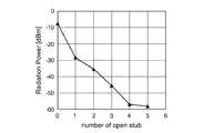
ちなみに、発明者は、電磁界解析を行い、バイアホール31に接続されるオープンスタブ32の数を変えながら、最下層の開口部30から放射される電力を算出した。図9は、放射される電力の算出結果を示す折れ線グラフである。横軸は、バイアホール31に接続されるオープンスタブ32の数を示し、縦軸は、放射された電力を示している。電磁界解析の結果、オープンスタブ32が数が多いほど、放射される電力が減少することがわかった(図9参照)。
Incidentally, the inventor performed an electromagnetic field analysis, and calculated the power radiated from the
また、例えば、各バイアホール31に設けられるオープンスタブ32の数は、同じでなくてもよい。
Further, for example, the number of
また、例えば、オープンスタブ32の形状はどのような形状であってもよい。例えば、2つの扇形を結合したような形状であってもよいし、半円形状であってもよいし、矩形形状であってもよい。
For example, the
また、例えば、金属ケース17と、強度変調制御IC20及び増幅IC22と、の間に電磁吸収体を配置してもよい。
Further, for example, an electromagnetic absorber may be disposed between the
また、例えば、上記光送受信機2は、複数のビットレート(例えば43Gbps及び44.6Gbpsの2つのビットレート)で動作するRZ−DQPSK方式の光送受信機であってもよい。
For example, the
また、上記実施形態では、光送受信機2が「光モジュール」であったが、以上に説明した強度変調制御部14を含む他のモジュールが「光モジュール」であってもよい。例えば、上記送信用モジュールが「光モジュール」であってもよい。また、強度変調制御部14を含む光伝送装置が「光モジュール」であってもよい。
In the above embodiment, the
2 光送受信機、3,5 ブッシュ、4 レーザ、6 光変調器モジュール、8 位相変調器、10 強度変調器、12 位相変調制御部、14 強度変調制御部、16 多層プリント基板、17 金属ケース、18 同軸コネクタ、20 強度変調制御IC、22 増幅IC、24 中心導体、26a,26b,26c マイクロストリップライン、28 表層銅箔パタン、30 開口部、31 バイアホール、32 オープンスタブ、33 グラウンド・ビア、34a,34b,34c,34d,34e 配線層。
2 optical transceiver, 3, 5 bush, 4 laser, 6 optical modulator module, 8 phase modulator, 10 intensity modulator, 12 phase modulation controller, 14 intensity modulation controller, 16 multilayer printed circuit board, 17 metal case, 18 Coaxial connector, 20 Intensity modulation control IC, 22 Amplifier IC, 24 Center conductor, 26a, 26b, 26c Microstrip line, 28 Surface copper foil pattern, 30 Opening, 31 Via hole, 32 Open stub, 33 Ground via, 34a, 34b, 34c, 34d, 34e Wiring layers.
Claims (7)
前記多層プリント基板に設置された同軸コネクタと、
光変調器による光変調を制御するための高周波クロック信号を生成し、前記同軸コネクタへと出力する変調制御回路と、
前記多層プリント基板上に形成された信号ラインであって、前記同軸コネクタと、前記多層プリント基板に設置された前記変調制御回路と、に接続された信号ラインと、
前記変調制御回路を覆う金属ケースと、
を含み、
前記複数の接地導体層は、第1の接地導体層と第2の接地導体層とを含み、
前記バイアホールから伸びるオープンスタブが、前記第1の接地導体層と前記第2の接地導体層との間の層に設けられていること、
を特徴とする光モジュール。 A multilayer printed board including a plurality of ground conductor layers, wherein a via hole is formed that is insulated from the plurality of ground conductor layers by an antipad provided over all of the plurality of ground conductor layers. When,
A coaxial connector installed on the multilayer printed circuit board;
A modulation control circuit that generates a high-frequency clock signal for controlling optical modulation by the optical modulator and outputs the signal to the coaxial connector;
A signal line formed on the multilayer printed board, the signal line connected to the coaxial connector and the modulation control circuit installed on the multilayer printed board,
A metal case covering the modulation control circuit;
Including
The plurality of ground conductor layers include a first ground conductor layer and a second ground conductor layer,
An open stub extending from the via hole is provided in a layer between the first ground conductor layer and the second ground conductor layer;
An optical module characterized by
を特徴とする請求項1に記載の光モジュール。 The length of the open stub is a length according to the frequency of the high-frequency clock signal;
The optical module according to claim 1.
を特徴とする請求項2に記載の光モジュール。 The length of the open stub is a length obtained by multiplying the wavelength corresponding to the high-frequency clock signal determined based on the frequency by n / 4 (n is an odd number).
The optical module according to claim 2.
同軸コネクタと、
前記増幅ICと前記同軸コネクタとを一方の面に搭載し、前記増幅ICの前記出力端子と前記同軸コネクタの中心導体とを接続する信号ラインを備えた多層プリント基板と、
前記多層プリント基板の前記一方の面に設けられ、前記同軸コネクタと前記増幅ICを覆う金属ケースと、を備え、
前記プリント基板は、第1および第2の接地導体層を含む、複数の接地導体層を備え、
前記一方の面に対して垂直となる方向に前記複数の接地導体層すべてを貫くバイアホールが形成されており、かつ前記バイアホールは前記金属ケースの下部領域に配置されており、
前記バイアホールと前記複数の接地導体層とはアンチパッドにより電気的に絶縁されており、
前記バイアホールに接続したオープンスタブが前記第1および前記第2の接地導体層との間に位置して設けられ、
前記オープンスタブの長さは、前記高周波クロック信号の周波数に対応する波長を4分のn(nは奇数)倍した長さであること、と特徴とした光モジュール。 An amplification IC having an output terminal for amplifying and outputting a high-frequency clock signal;
A coaxial connector;
A multilayer printed circuit board having a signal line for mounting the amplification IC and the coaxial connector on one surface and connecting the output terminal of the amplification IC and a central conductor of the coaxial connector;
A metal case provided on the one surface of the multilayer printed board and covering the coaxial connector and the amplifier IC;
The printed circuit board includes a plurality of ground conductor layers including first and second ground conductor layers;
A via hole penetrating all of the plurality of ground conductor layers is formed in a direction perpendicular to the one surface, and the via hole is disposed in a lower region of the metal case;
The via hole and the plurality of ground conductor layers are electrically insulated by an antipad,
An open stub connected to the via hole is provided between the first and second ground conductor layers;
The length of the open stub is a length obtained by multiplying the wavelength corresponding to the frequency of the high-frequency clock signal by n / 4 (n is an odd number).
前記多層プリント基板の、前記金属ケースの下部領域に、前記複数の接地導体層および前記信号ラインと絶縁されている前記バイアホールが複数形成され、
前記複数のバイアホールそれぞれから伸びる前記オープンスタブが前記第1の接地導体層と前記第2の接地導体層との間の層に設けられ、前記オープンスタブは扇形形状、二つの扇形を結合した形状、半円形状、または矩形形状のいずれかの形状であること、を特徴とする光モジュール。 The optical module according to claim 1,
A plurality of via holes insulated from the plurality of ground conductor layers and the signal lines are formed in a lower region of the metal case of the multilayer printed circuit board,
The open stub extending from each of the plurality of via holes is provided in a layer between the first ground conductor layer and the second ground conductor layer, and the open stub has a fan shape and a shape in which two fan shapes are combined. An optical module characterized by having a semicircular shape or a rectangular shape.
前記バイアホールから伸びる他のオープンスタブが前記第1の接地導体層と前記第2の接地導体層間以外の他の隣り合う接地導体層間に設けられていること、を特徴とする光モジュール。 The optical module according to claim 4 or 5,
An optical module, wherein another open stub extending from the via hole is provided between adjacent ground conductor layers other than the first ground conductor layer and the second ground conductor layer.
前記オープンスタブは、扇形形状、二つの扇形を結合した形状、半円形状、または矩形形状のいずれかの形状であること、を特徴とする光モジュール。
The optical module according to any one of claims 1 to 6,
The optical module is characterized in that the open stub has a fan shape, a shape obtained by combining two fan shapes, a semicircular shape, or a rectangular shape.
Priority Applications (2)
| Application Number | Priority Date | Filing Date | Title |
|---|---|---|---|
| JP2010019362A JP5675122B2 (en) | 2010-01-29 | 2010-01-29 | Optical module |
| US13/015,769 US8467118B2 (en) | 2010-01-29 | 2011-01-28 | Optical module |
Applications Claiming Priority (1)
| Application Number | Priority Date | Filing Date | Title |
|---|---|---|---|
| JP2010019362A JP5675122B2 (en) | 2010-01-29 | 2010-01-29 | Optical module |
Publications (3)
| Publication Number | Publication Date |
|---|---|
| JP2011159742A JP2011159742A (en) | 2011-08-18 |
| JP2011159742A5 JP2011159742A5 (en) | 2012-12-06 |
| JP5675122B2 true JP5675122B2 (en) | 2015-02-25 |
Family
ID=44341442
Family Applications (1)
| Application Number | Title | Priority Date | Filing Date |
|---|---|---|---|
| JP2010019362A Active JP5675122B2 (en) | 2010-01-29 | 2010-01-29 | Optical module |
Country Status (2)
| Country | Link |
|---|---|
| US (1) | US8467118B2 (en) |
| JP (1) | JP5675122B2 (en) |
Families Citing this family (3)
| Publication number | Priority date | Publication date | Assignee | Title |
|---|---|---|---|---|
| JP2010123640A (en) | 2008-11-17 | 2010-06-03 | Opnext Japan Inc | Printed circuit board and optical transmitting apparatus |
| JP5661137B2 (en) * | 2013-04-11 | 2015-01-28 | 日本オクラロ株式会社 | Printed circuit board and optical transmission device |
| JP6654155B2 (en) * | 2017-01-10 | 2020-02-26 | Kddi株式会社 | Optical transmission system, PON system and transmission method |
Family Cites Families (12)
| Publication number | Priority date | Publication date | Assignee | Title |
|---|---|---|---|---|
| JPH02167525A (en) * | 1988-12-21 | 1990-06-27 | Fujitsu Ltd | Optical modulation device |
| JPH03198402A (en) * | 1989-12-26 | 1991-08-29 | Matsushita Electric Ind Co Ltd | Microwave circuit, bias circuit, and band stop filter |
| JPH10290075A (en) * | 1997-04-14 | 1998-10-27 | Murata Mfg Co Ltd | Multilayered circuit board |
| JPH10341027A (en) * | 1997-06-10 | 1998-12-22 | Nippon Telegr & Teleph Corp <Ntt> | Optical module |
| JP2004004317A (en) * | 2002-05-31 | 2004-01-08 | Mitsubishi Electric Corp | Optical modulator |
| JP2005044963A (en) * | 2003-07-28 | 2005-02-17 | Tdk Corp | Laser diode module |
| JP4633455B2 (en) * | 2004-12-24 | 2011-02-16 | 富士通セミコンダクター株式会社 | Semiconductor device |
| JP4657860B2 (en) | 2005-09-16 | 2011-03-23 | 富士通株式会社 | Optical transmitter and optical communication system |
| JP2008090093A (en) * | 2006-10-04 | 2008-04-17 | Nippon Telegr & Teleph Corp <Ntt> | Single-core bidirectional optical transmission and reception transceiver |
| JP2009129649A (en) * | 2007-11-21 | 2009-06-11 | Murata Mfg Co Ltd | Connector mounting portion structure on board |
| JP2010123640A (en) | 2008-11-17 | 2010-06-03 | Opnext Japan Inc | Printed circuit board and optical transmitting apparatus |
| JP5334686B2 (en) * | 2009-05-27 | 2013-11-06 | 三菱電機株式会社 | Multi-layer high frequency package substrate |
-
2010
- 2010-01-29 JP JP2010019362A patent/JP5675122B2/en active Active
-
2011
- 2011-01-28 US US13/015,769 patent/US8467118B2/en active Active
Also Published As
| Publication number | Publication date |
|---|---|
| US20110188108A1 (en) | 2011-08-04 |
| JP2011159742A (en) | 2011-08-18 |
| US8467118B2 (en) | 2013-06-18 |
Similar Documents
| Publication | Publication Date | Title |
|---|---|---|
| CN108415182B (en) | Optical modulator with FPC and optical transmitter using the same | |
| JP5216147B2 (en) | Differential transmission circuit, optical transceiver module, and information processing apparatus | |
| JP5859219B2 (en) | Differential transmission line and communication device | |
| JP5072968B2 (en) | Waveguide connection structure | |
| US8660434B2 (en) | Printed circuit board and optical transmission device | |
| JP4852442B2 (en) | Optical transmission module | |
| US11224120B2 (en) | Print circuit board, optical module, and optical transmission equipment | |
| US10921620B2 (en) | Optical modulator and optical transmission apparatus | |
| JP7000964B2 (en) | Multi-layer transmission line | |
| JP5146267B2 (en) | Manufacturing method of wiring board and printed wiring board | |
| JP5675122B2 (en) | Optical module | |
| JP4519086B2 (en) | Patch antennas and high frequency devices | |
| JP2008283676A (en) | High frequency sensor apparatus | |
| JP4532509B2 (en) | In-vehicle radio radar equipment | |
| JP2010016076A (en) | Flexible printed board and rigid flexible printed board provided therewith | |
| KR20200129341A (en) | Flexible cable | |
| JPWO2011102300A1 (en) | Waveguide / planar line converter | |
| JP2009100168A (en) | Transmission and reception module | |
| CN108700761B (en) | Optical modulator with FPC and optical transmission device using the same | |
| JP4795225B2 (en) | Dielectric waveguide slot antenna | |
| JP2019201197A (en) | Interlayer transmission line | |
| JP2004303752A (en) | Semiconductor device and optical transceiver | |
| JP5661137B2 (en) | Printed circuit board and optical transmission device | |
| WO2022215713A1 (en) | Antenna device | |
| WO2021065459A1 (en) | High-frequency shield structure |
Legal Events
| Date | Code | Title | Description |
|---|---|---|---|
| A621 | Written request for application examination |
Free format text: JAPANESE INTERMEDIATE CODE: A621 Effective date: 20120312 |
|
| A521 | Request for written amendment filed |
Free format text: JAPANESE INTERMEDIATE CODE: A523 Effective date: 20121024 |
|
| A977 | Report on retrieval |
Free format text: JAPANESE INTERMEDIATE CODE: A971007 Effective date: 20130123 |
|
| A131 | Notification of reasons for refusal |
Free format text: JAPANESE INTERMEDIATE CODE: A131 Effective date: 20130806 |
|
| A521 | Request for written amendment filed |
Free format text: JAPANESE INTERMEDIATE CODE: A523 Effective date: 20131004 |
|
| A131 | Notification of reasons for refusal |
Free format text: JAPANESE INTERMEDIATE CODE: A131 Effective date: 20140218 |
|
| A521 | Request for written amendment filed |
Free format text: JAPANESE INTERMEDIATE CODE: A523 Effective date: 20140418 |
|
| A131 | Notification of reasons for refusal |
Free format text: JAPANESE INTERMEDIATE CODE: A131 Effective date: 20140805 |
|
| A521 | Request for written amendment filed |
Free format text: JAPANESE INTERMEDIATE CODE: A523 Effective date: 20141001 |
|
| TRDD | Decision of grant or rejection written | ||
| A01 | Written decision to grant a patent or to grant a registration (utility model) |
Free format text: JAPANESE INTERMEDIATE CODE: A01 Effective date: 20141216 |
|
| A61 | First payment of annual fees (during grant procedure) |
Free format text: JAPANESE INTERMEDIATE CODE: A61 Effective date: 20141224 |
|
| R150 | Certificate of patent or registration of utility model |
Ref document number: 5675122 Country of ref document: JP Free format text: JAPANESE INTERMEDIATE CODE: R150 |
|
| R250 | Receipt of annual fees |
Free format text: JAPANESE INTERMEDIATE CODE: R250 |
|
| R250 | Receipt of annual fees |
Free format text: JAPANESE INTERMEDIATE CODE: R250 |
|
| S533 | Written request for registration of change of name |
Free format text: JAPANESE INTERMEDIATE CODE: R313533 |
|
| R350 | Written notification of registration of transfer |
Free format text: JAPANESE INTERMEDIATE CODE: R350 |
|
| R250 | Receipt of annual fees |
Free format text: JAPANESE INTERMEDIATE CODE: R250 |
|
| R250 | Receipt of annual fees |
Free format text: JAPANESE INTERMEDIATE CODE: R250 |
|
| R250 | Receipt of annual fees |
Free format text: JAPANESE INTERMEDIATE CODE: R250 |
|
| R250 | Receipt of annual fees |
Free format text: JAPANESE INTERMEDIATE CODE: R250 |
|
| R250 | Receipt of annual fees |
Free format text: JAPANESE INTERMEDIATE CODE: R250 |