JP4532509B2 - In-vehicle radio radar equipment - Google Patents
In-vehicle radio radar equipment Download PDFInfo
- Publication number
- JP4532509B2 JP4532509B2 JP2007008039A JP2007008039A JP4532509B2 JP 4532509 B2 JP4532509 B2 JP 4532509B2 JP 2007008039 A JP2007008039 A JP 2007008039A JP 2007008039 A JP2007008039 A JP 2007008039A JP 4532509 B2 JP4532509 B2 JP 4532509B2
- Authority
- JP
- Japan
- Prior art keywords
- circuit board
- radio wave
- radar device
- housing
- connector
- Prior art date
- Legal status (The legal status is an assumption and is not a legal conclusion. Google has not performed a legal analysis and makes no representation as to the accuracy of the status listed.)
- Expired - Fee Related
Links
Images


Classifications
-
- G—PHYSICS
- G01—MEASURING; TESTING
- G01S—RADIO DIRECTION-FINDING; RADIO NAVIGATION; DETERMINING DISTANCE OR VELOCITY BY USE OF RADIO WAVES; LOCATING OR PRESENCE-DETECTING BY USE OF THE REFLECTION OR RERADIATION OF RADIO WAVES; ANALOGOUS ARRANGEMENTS USING OTHER WAVES
- G01S13/00—Systems using the reflection or reradiation of radio waves, e.g. radar systems; Analogous systems using reflection or reradiation of waves whose nature or wavelength is irrelevant or unspecified
- G01S13/88—Radar or analogous systems specially adapted for specific applications
- G01S13/93—Radar or analogous systems specially adapted for specific applications for anti-collision purposes
- G01S13/931—Radar or analogous systems specially adapted for specific applications for anti-collision purposes of land vehicles
-
- G—PHYSICS
- G01—MEASURING; TESTING
- G01S—RADIO DIRECTION-FINDING; RADIO NAVIGATION; DETERMINING DISTANCE OR VELOCITY BY USE OF RADIO WAVES; LOCATING OR PRESENCE-DETECTING BY USE OF THE REFLECTION OR RERADIATION OF RADIO WAVES; ANALOGOUS ARRANGEMENTS USING OTHER WAVES
- G01S7/00—Details of systems according to groups G01S13/00, G01S15/00, G01S17/00
- G01S7/02—Details of systems according to groups G01S13/00, G01S15/00, G01S17/00 of systems according to group G01S13/00
- G01S7/027—Constructional details of housings, e.g. form, type, material or ruggedness
Description
この発明は、車に取付けられ、レーダビームを放射し、被検出物体により反射されたレーダビームを受けて、この車から被検出物体までの距離等を検出する車載電波レーダ装置に関する。 The present invention relates to an on-vehicle radio wave radar device that is attached to a vehicle, radiates a radar beam, receives a radar beam reflected by a detected object, and detects a distance from the vehicle to the detected object.
従来、シールドカバーを用いて、内部の回路基板をシールドし、前記回路基板と電気的に接続され、外部装置と接続可能なコネクタのピンの外周面に貫通コンデンサの内周面を接続させ、前記貫通コンデンサの外周面を前記シールドカバーに接続させたフィルタコネクタが知られている(例えば、特許文献1参照)。
このフィルタコネクタは、前記ピンを通過するノイズを前記貫通コンデンサにより前記シールドカバーへ伝達することで、前記ピンから空間へ放射されるノイズを抑制する。
Conventionally, using a shield cover, the internal circuit board is shielded, electrically connected to the circuit board, and the inner peripheral surface of the feedthrough capacitor is connected to the outer peripheral surface of the connector pin connectable to an external device, A filter connector in which the outer peripheral surface of a feedthrough capacitor is connected to the shield cover is known (for example, see Patent Document 1).
The filter connector suppresses noise radiated from the pin to the space by transmitting noise passing through the pin to the shield cover by the feedthrough capacitor.
しかしながら、このコネクタフィルタの場合、高価な貫通コンデンサを用いているので、全体として、コストが非常に高くなってしまうという問題点があった。 However, in the case of this connector filter, since an expensive feedthrough capacitor is used, there is a problem that the cost becomes very high as a whole.
この発明は、上述のような問題点を解決することを課題とするものであって、その目的は、コストの上昇を抑制しつつ、コネクタのピンから放射されるノイズが筐体内の回路基板全体に広がることを抑制する車載電波レーダ装置を提供するものである。 An object of the present invention is to solve the above-described problems. The object of the present invention is to reduce noise radiated from the connector pins while suppressing an increase in cost. It is intended to provide an in-vehicle radio wave radar device that suppresses the spread.
この発明に係る車載電波レーダ装置は、車に取付けられ、レーダビームを放射し、被検出物体により反射された前記レーダビームを受けて、前記車から前記被検出物体までの距離および前記車と前記被検出物体との相対速度の少なくとも一方を検出する車載電波レーダ装置において、導電性の筐体と、前記筐体の内部に設けられ、少なくとも表層に形成されたグランドプレーンを有した回路基板と、ピンが前記回路基板に接続され、前記筐体の外部に設けられた外部装置と電気的に接続可能なコネクタと、前記筐体の内部に前記筐体と接続して設けられ、前記グランドプレーンと接続し、前記筐体と協同して、前記筐体内のコネクタを内包するコネクタ内包空間を形成した導電性の仕切り板とを備え、前記筐体と前記仕切り板とにより、前記ピンから空間へ放射されたノイズが前記コネクタ内包空間の外へ放出されるのを抑制し、前記回路基板は複数層の前記グランドプレーンを有した多層基板であり、前記コネクタと接続された前記回路基板内の信号パターンは、前記グランドプレーンの間に挟まれている。
An in-vehicle radio wave radar device according to the present invention is attached to a vehicle, radiates a radar beam, receives the radar beam reflected by a detected object, and determines the distance from the vehicle to the detected object and the vehicle and the In an in-vehicle radio wave radar device that detects at least one of relative speeds with respect to an object to be detected, a conductive housing, a circuit board provided inside the housing, and having a ground plane formed at least on the surface layer , A pin is connected to the circuit board and is electrically connected to an external device provided outside the housing, and is provided inside the housing in connection with the housing, and the ground plane A conductive partition plate that is connected and cooperates with the housing to form a connector enclosing space that encloses the connector in the housing, and the housing and the partition plate Emitted from the emission to the space noise is prevented from being discharged to the outside of the connector containing space, said circuit board is a multilayer board having the ground plane of a plurality layers, the connector and connected to said circuit The signal pattern in the substrate is sandwiched between the ground planes .
この発明に係る車載電波レーダ装置によれば、コストの上昇を抑制しつつ、コネクタかのピンから放射されるノイズが筐体内の回路基板全体に広がることを抑制することができる。 According to the in-vehicle radio wave radar device according to the present invention, it is possible to suppress the noise radiated from the pins of the connector from spreading to the entire circuit board in the housing while suppressing an increase in cost.
以下、この発明の各実施の形態を図に基づいて説明するが、各図において、同一または相当の部材、部位については、同一符号を付して説明する。
実施の形態1.
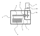
図1は実施の形態1に係る車載電波レーダ装置1のブロック図、図2は図1の車載電波レーダ装置1の断面図、図3は図1の信号処理回路基板3と仕切り板7との関係を示す平面図である。
実施の形態1に係る車載電波レーダ装置1は、導電性の筐体2と、この筐体2の内部に設けられた回路基板である、信号処理回路基板3およびRF送受信回路基板4と、ピン5aが信号処理回路基板3に接続され、筐体2の外部に設けられた外部装置(図示せず)と電気的に接続可能なコネクタ5と、筐体2の内部に筐体2と電気的に接続して設けられ、信号処理回路基板3のグランドプレーン6と電気的に接続し、筐体2とともに筐体2内部のコネクタ5を内包するコネクタ内包空間2aを形成した導電性の仕切り板7とを備えている。
Hereinafter, embodiments of the present invention will be described with reference to the drawings. In the drawings, the same or corresponding members and parts will be described with the same reference numerals.
1 is a block diagram of an in-vehicle
The in-vehicle radio
信号処理回路基板3上には、コネクタ5に接続されたインターフェース8と、このインターフェース8に接続され、コネクタ5からの信号を処理する信号処理回路9と、この信号処理回路9の制御により、デジタルの信号を送信する周波数制御データ格納メモリ10とが搭載されている。
また、信号処理回路基板3上には、周波数制御データ格納メモリ10からの信号をデジタルからアナログに変換するD/A変換器11と、後述するIFアンプ22からの信号をアナログからデジタルに変換し、信号処理回路9に送信するA/D変換器12とが搭載されている。
グランドプレーン6は、仕切り板7と当接するように、信号処理回路基板3の両面に設けられている。なお、このグランドプレーン6は、コネクタ5の複数あるピン5aの中のグランド線とも接続されている。
アナログの信号が流れる電気回路は、微小な信号を扱っており、ノイズに対する耐性が低い。
On the signal
On the signal
The ground plane 6 is provided on both surfaces of the signal
An electric circuit through which an analog signal flows handles a minute signal and has low resistance to noise.
RF送受信回路基板4上には、D/A変換器11からの信号が入力される電圧制御発振器13と、この電圧制御発振器13から出力される信号を分岐するパワーデバイダ14と、このパワーデバイダ14から出力される信号を増幅させる送信アンプ15と、この送信アンプ15からの信号をレーダビームとして放射する送信アンテナ16とが搭載されている。
また、RF送受信回路基板4上には、被検出物体17から反射されたレーダビームを受信する受信アンテナ18と、この受信アンテナ18からの信号を増幅する受信アンプ19と、この受信アンプ19からの信号と、パワーデバイダ14により分岐された電圧制御発振器13からの信号とを比較する受信ミキサ20と、この受信ミキサ20からの信号にフィルタをかけるフィルタ21と、このフィルタ21からの信号を増幅させるIFアンプ22とが搭載されている。
送信アンテナ16および受信アンテナ18に対向した筐体2の面には、送信アンテナ16および受信アンテナ18を保護するレドーム23が設けられている。
On the RF transmission /
Further, on the RF transmission /
A
コネクタ5は、筐体2の側面にネジ24を介して固定されており、L字形状をしたコネクタ5のピン5aはロウ材である半田を介して信号処理回路基板3に垂直に接続されている。
ピン5aは、筐体2と仕切り板7とにより囲まれており、この筐体2および仕切り板7は、信号処理回路基板3のグランドプレーン6と電気的に接続されているので、ピン5aから空間へ放射されたノイズは、筐体2および仕切り板7により形成されるコネクタ内包空間2aの外へ放出されることが抑制され、信号処理回路9および周波数制御データ格納メモリ10等へノイズが伝達されるのを抑制することができる。
The
The
以上説明したように、実施の形態1に係る車載電波レーダ装置1によれば、ピン5aを覆う筐体2および仕切り板7により、ピン5aから空間へ放出されたノイズがコネクタ内包空間2aの外へ放出されることが抑制されるので、高価な貫通コンデンサを用いずに、コネクタ内包空間2aの外側であって筐体2内部の空間にある信号処理回路基板3およびRF送受信回路基板4へノイズが影響することを抑制することができる。
As described above, according to the in-vehicle radio
なお、上記実施の形態1では、コネクタ5のピン5aがL字形状をして、信号処理回路基板3に接続された車載電波レーダ装置1について説明したが、図4に示すように、コネクタ5のピン5aがまっすぐで、信号処理回路基板3に接続された車載電波レーダ装置1であってもよい。
In the first embodiment, the in-vehicle radio
実施の形態2.
図5は実施の形態2に係る車載電波レーダ装置1の断面図、図6は図5の信号処理回路基板3を示す平面図である。
筐体2の内部には、信号処理回路基板3がネジ25により筐体2に固定されている。この信号処理回路基板3は、図示しないRF送受信回路基板4に接続されている。
信号処理回路基板3の一方の面にはコネクタ5が設けられ、このコネクタ5のピン5aは信号処理回路基板3に貫通して、接続されている。
ピン5aと接続する信号処理回路基板3の両面には、導電性の接続パターン29が設けられ、ピン5aと接続パターン29とが半田を介して電気的に接続されている。
また、信号処理回路基板3のコネクタ5が取付けられた面と同じ面には、面実装型のセラミックコンデンサ26が設けられている。
仕切り板7と当接する信号処理回路基板3の両面には、グランドプレーン6が設けられており、グランドプレーン6は、仕切り板7と電気的に接続されている。
仕切り板7は、筐体2と電気的に接続されており、筐体2とともにコネクタ内包空間2aを形成する。
セラミックコンデンサ26は、一端部が接続パターン29を介してピン5aと電気的に接続され、他端部がグランドプレーン6を介して仕切り板7と電気的に接続されている。
ピン5a、セラミックコンデンサ26および仕切り板7は、それぞれが近接して配置されている。
その他の構成は実施の形態1と同様である。
FIG. 5 is a cross-sectional view of the in-vehicle radio
Inside the
A
A surface mounting type
Ground planes 6 are provided on both surfaces of the signal
The
One end of the
The
Other configurations are the same as those of the first embodiment.
実施の形態2に係る車載電波レーダ装置1によれば、ピン5aと仕切り板7との間にセラミックコンデンサ26が電気的に接続されているので、ピン5aを伝達するノイズがセラミックコンデンサ26を介して仕切り板7に伝わるので、信号処理回路基板3の全体にノイズが伝達されることを抑制することができる。
According to the in-vehicle radio
また、コンデンサは、セラミックコンデンサ26であるので、貫通コンデンサより単価が安く、それぞれのピン5aに設けても、コストの上昇を抑制することができる。
Further, since the capacitor is the
また、セラミックコンデンサ26が信号処理回路基板3におけるコネクタ5と同一面に設けられ、この面がコネクタ5を半田付けするために半田を付着させる面とは逆の面であるので、先にセラミックコンデンサ26を取付け、後でコネクタ5を取付けることができる。その結果、セラミックコンデンサ26とコネクタ5との距離を近づけることができ、ピン5aを伝達するノイズを仕切り板7に向かって一層伝えることができる。
Further, the
実施の形態3.
図7は実施の形態3に係る車載電波レーダ装置1の断面図である。
コネクタ5のピン5aは、信号ピン28aおよびグランドピン28bから構成され、信号ピン28aは信号処理回路基板3上の接続パターン29と接続され、グランドピン28bは後述する当接グランドプレーン6aおよび内層グランドプレーン6bと接続されている。
信号処理回路基板3は5層の金属パターンから構成された5層基板である。
信号処理回路基板3の両面にある最も外側の層であって、仕切り板7と当接する近傍では、仕切り板7と当接し電気的に接続された当接グランドプレーン6aが設けられている。
信号処理回路基板3の真ん中の層には、コネクタ5の信号ピン28aと接続された信号パターン30が設けられ、この信号パターン30の両面と当接グランドプレーン6aとの間には、グランドピン28bを介して当接グランドプレーン6aと接続された内層グランドプレーン6bが設けられている。
信号処理回路基板3においてコネクタ5と同一の面であって、当接グランドプレーン6aと接続パターン29との間には、セラミックコンデンサ26が接続されている。
なお、図7中の黒丸は、電気的に接続されていることを示している。
その他の構成は実施の形態2と同様である。
FIG. 7 is a sectional view of the in-vehicle radio
The
The signal
In the vicinity of the outermost layer on both surfaces of the signal
A
A
Note that black circles in FIG. 7 indicate that they are electrically connected.
Other configurations are the same as those of the second embodiment.
実施の形態3に係る車載電波レーダ装置1によれば、信号処理回路基板3が5層基板であり、信号処理回路基板3の内部に設けられ、仕切り板7と電気的に接続された2層の内層グランドプレーン6bにより、コネクタ5の信号ピン28aと電気的に接続された信号パターン30が挟まれているので、信号ピン28aから放射されたノイズが、信号パターン30へ伝わるのを抑制することができる。
According to the in-vehicle radio
実施の形態4.
図8は実施の形態4に係る車載電波レーダ装置1の信号処理回路基板3を示す平面図である。
信号処理回路基板3のグランドプレーン6における仕切り板7と当接する領域には、変形可能な半田である導電体27が盛られている。
導電体27は、仕切り板7の当接面に沿って、連続的に設けられており、仕切り板7をグランドプレーン6に当接させる際に、仕切り板7の端面の形状に合わせて変形可能である。
その他の構成は、実施の形態3と同様である。
FIG. 8 is a plan view showing the signal
A
The
Other configurations are the same as those of the third embodiment.
実施の形態4に係る車載電波レーダ装置1によれば、仕切り板7と信号処理回路基板3のグランドプレーン6との間に導電体27が設けられているので、仕切り板7をグランドプレーン6に当接させる際に、仕切り板7とグランドプレーン6との電気的接続が向上する。その結果、コネクタ5のピン5aから伝達され、信号パターン30を伝達するノイズを筐体2へ一層伝えることができる。
According to the on-vehicle radio
また、導電体27として半田を用いて、仕切り板7とグランドプレーン6との電気的接続を向上させるので、簡単に信号パターン30を通過するノイズを筐体2へ伝えることができる。
Moreover, since the electrical connection between the
実施の形態5.
図9は実施の形態5に係る車載電波レーダ装置1の信号処理回路基板3を示す平面図である。
信号処理回路基板3のグランドプレーン6における仕切り板7と当接する領域には、長方形形状をした半田である複数の導電部27aが所定の間隔をおいて配置されている。
その他の構成は実施の形態4と同様である。
導電部27aが間隔をおいて配置されているので、仕切り板7をグランドプレーン6に当接させる際に、仕切り板7の端面の形状に合わせて一層変形可能である。
なお、隣接した導電部27aの間隔は、コネクタ内包空間2aの外への放出を抑制したいノイズの周波数の波長から算出すればよい。
FIG. 9 is a plan view showing the signal
In a region of the ground plane 6 of the signal
Other configurations are the same as those in the fourth embodiment.
Since the
In addition, what is necessary is just to calculate the space | interval of the adjacent
実施の形態5に係る車載電波レーダ装置1によれば、複数の導電部27aが間隔をおいて信号処理回路基板3のグランドプレーン6上に設けられているので、仕切り板7とグランドプレーン6との電気的接続を一層向上させることができる。その結果、コネクタ5のピン5aから伝達され、信号パターン30を伝達するノイズを筐体2へ一層伝達させることができる。
According to the on-vehicle radio
また、導電部27aが、長方形形状をしているので、仕切り板7との当接により容易に変形し、仕切り板7とグランドプレーン6との電気的接続を一層向上させることができる。
Further, since the
実施の形態6.
図10は実施の形態6に係る車載電波レーダ装置1の信号処理回路基板3を示す平面図である。
信号処理回路基板3のグランドプレーン6における仕切り板7と当接する領域には、丸形状をした半田である複数の導電部27bが所定の間隔をおいて配置されている。
その他の構成は実施の形態5と同様である。
丸形状をした導電部27bが間隔をおいて配置されているので、導電部27bは、仕切り板7による当接により一層変形しやすく、仕切り板7の端面の形状に合わせて一層変形可能である。
Embodiment 6 FIG.
FIG. 10 is a plan view showing the signal
In a region of the ground plane 6 of the signal
Other configurations are the same as those of the fifth embodiment.
Since the round
実施の形態6に係る車載電波レーダ装置1によれば、丸形状の複数の導電部27bが間隔をおいて信号処理回路基板3のグランドプレーン6上に設けられているので、仕切り板7とグランドプレーン6との電気的接続を一層向上させることができる。その結果、コネクタ5からのピン5aから伝達され、信号パターン30を伝達するノイズを筐体2へ一層伝えることができる。
According to the in-vehicle radio
なお、上記実施の形態4ないし上記実施の形態6では、変形可能な導電体27を半田とし、また、導電体27を構成する複数の導電部27a、27bを半田とした車載電波レーダ装置1について説明したが、勿論このものに限らず、その他の変形可能なロウ材であってもよい。
In the fourth to sixth embodiments described above, the in-vehicle radio
また、上記実施の形態2ないし上記実施の形態6では、コンデンサを面実装型のセラミックコンデンサ26とした車載電波レーダ装置1について説明したが、勿論このものに限らず、貫通型以外であればよく、例えば、リード型のコンデンサを備えた車載電波レーダ装置1であってもよい。また、セラミックコンデンサ26とは限らず、例えば、電解コンデンサ等の他の材料により構成されたコンデンサを備えた車載電波レーダ装置1であってもよい。
In the second to sixth embodiments, the on-vehicle radio
1 車載電波レーダ装置、2 筐体、2a コネクタ内包空間、3 信号処理回路基板、4 RF送受信回路基板、5 コネクタ、5a ピン、6 グランドプレーン、6a 当接グランドプレーン、6b 内層グランドプレーン、7 仕切り板、8 インターフェース、9 信号処理回路、10 周波数制御データ格納メモリ、11 D/A変換器、12 A/D変換器、13 電圧制御発振器、14 パワーデバイダ、15 送信アンプ、16 送信アンテナ、17 被検出物体、18 受信アンテナ、19 受信アンプ、20 受信ミキサ、21 フィルタ、22 IFアンプ、23 レドーム、24 ネジ、25 ネジ、26 セラミックコンデンサ、27 導電体、27a 導電部、27b 導電部、28a 信号ピン、28b グランドピン、29 接続パターン、30 信号パターン。
DESCRIPTION OF
Claims (9)
導電性の筐体と、
前記筐体の内部に設けられ、少なくとも表層に形成されたグランドプレーンを有した回路基板と、
ピンが前記回路基板に接続され、前記筐体の外部に設けられた外部装置と電気的に接続可能なコネクタと、
前記筐体の内部に前記筐体と接続して設けられ、前記グランドプレーンと接続し、前記筐体と協同して、前記筐体内のコネクタを内包するコネクタ内包空間を形成した導電性の仕切り板とを備え、
前記筐体と前記仕切り板とにより、前記ピンから空間へ放射されたノイズが前記コネクタ内包空間の外へ放出されるのを抑制し、
前記回路基板は複数層の前記グランドプレーンを有した多層基板であり、前記コネクタと接続された前記回路基板内の信号パターンは、前記グランドプレーンの間に挟まれていることを特徴とする車載電波レーダ装置。 At least one of a distance from the vehicle to the detected object and a relative speed between the vehicle and the detected object, the radar beam being attached to the car, radiating a radar beam, receiving the radar beam reflected by the detected object In-vehicle radio wave radar device that detects
A conductive housing;
A circuit board provided in the housing and having a ground plane formed at least on the surface layer ;
A connector having pins connected to the circuit board and electrically connectable to an external device provided outside the housing;
A conductive partition plate provided inside the housing in connection with the housing, connected to the ground plane , and in cooperation with the housing to form a connector enclosing space that encloses the connector in the housing. And
The housing and the partition plate prevent noise radiated from the pin to the space from being released outside the connector enclosure space ,
The circuit board is a multilayer board having a plurality of ground planes, and a signal pattern in the circuit board connected to the connector is sandwiched between the ground planes. Radar device.
Priority Applications (1)
| Application Number | Priority Date | Filing Date | Title |
|---|---|---|---|
| JP2007008039A JP4532509B2 (en) | 2007-01-17 | 2007-01-17 | In-vehicle radio radar equipment |
Applications Claiming Priority (1)
| Application Number | Priority Date | Filing Date | Title |
|---|---|---|---|
| JP2007008039A JP4532509B2 (en) | 2007-01-17 | 2007-01-17 | In-vehicle radio radar equipment |
Publications (2)
| Publication Number | Publication Date |
|---|---|
| JP2008175622A JP2008175622A (en) | 2008-07-31 |
| JP4532509B2 true JP4532509B2 (en) | 2010-08-25 |
Family
ID=39702757
Family Applications (1)
| Application Number | Title | Priority Date | Filing Date |
|---|---|---|---|
| JP2007008039A Expired - Fee Related JP4532509B2 (en) | 2007-01-17 | 2007-01-17 | In-vehicle radio radar equipment |
Country Status (1)
| Country | Link |
|---|---|
| JP (1) | JP4532509B2 (en) |
Families Citing this family (3)
| Publication number | Priority date | Publication date | Assignee | Title |
|---|---|---|---|---|
| DE102008062190A1 (en) * | 2008-12-13 | 2010-06-17 | Valeo Schalter Und Sensoren Gmbh | Plug connections to radar sensors and method for their production |
| JP5307067B2 (en) * | 2010-03-30 | 2013-10-02 | 古河電気工業株式会社 | Automotive pulse radar |
| JP7251215B2 (en) * | 2019-03-01 | 2023-04-04 | 株式会社デンソー | Automotive radar equipment |
Citations (7)
| Publication number | Priority date | Publication date | Assignee | Title |
|---|---|---|---|---|
| JPH0620746A (en) * | 1992-07-03 | 1994-01-28 | Murata Mfg Co Ltd | Surface installation type connector |
| JPH0935823A (en) * | 1995-07-18 | 1997-02-07 | Japan Aviation Electron Ind Ltd | Filter connector |
| JPH1022672A (en) * | 1996-07-08 | 1998-01-23 | Iwaki Electron Corp Ltd | High frequency module |
| JP2000286587A (en) * | 1999-03-30 | 2000-10-13 | Matsushita Electric Ind Co Ltd | Electromagnetic shield structure at connector part with external cable |
| JP2003152585A (en) * | 2001-11-19 | 2003-05-23 | Hitachi Ltd | On-vehicle signal processor and on-vehicle radar apparatus |
| JP2006093421A (en) * | 2004-09-24 | 2006-04-06 | Mitsubishi Electric Corp | High-frequency device |
| JP2006210849A (en) * | 2005-01-31 | 2006-08-10 | Orion Denki Kk | Analog/digital recordable and reproducible apparatus and display device |
-
2007
- 2007-01-17 JP JP2007008039A patent/JP4532509B2/en not_active Expired - Fee Related
Patent Citations (7)
| Publication number | Priority date | Publication date | Assignee | Title |
|---|---|---|---|---|
| JPH0620746A (en) * | 1992-07-03 | 1994-01-28 | Murata Mfg Co Ltd | Surface installation type connector |
| JPH0935823A (en) * | 1995-07-18 | 1997-02-07 | Japan Aviation Electron Ind Ltd | Filter connector |
| JPH1022672A (en) * | 1996-07-08 | 1998-01-23 | Iwaki Electron Corp Ltd | High frequency module |
| JP2000286587A (en) * | 1999-03-30 | 2000-10-13 | Matsushita Electric Ind Co Ltd | Electromagnetic shield structure at connector part with external cable |
| JP2003152585A (en) * | 2001-11-19 | 2003-05-23 | Hitachi Ltd | On-vehicle signal processor and on-vehicle radar apparatus |
| JP2006093421A (en) * | 2004-09-24 | 2006-04-06 | Mitsubishi Electric Corp | High-frequency device |
| JP2006210849A (en) * | 2005-01-31 | 2006-08-10 | Orion Denki Kk | Analog/digital recordable and reproducible apparatus and display device |
Also Published As
| Publication number | Publication date |
|---|---|
| JP2008175622A (en) | 2008-07-31 |
Similar Documents
| Publication | Publication Date | Title |
|---|---|---|
| US6842093B2 (en) | Radio frequency circuit module on multi-layer substrate | |
| US7728780B2 (en) | Antenna device and information terminal device | |
| JP4990353B2 (en) | High frequency package | |
| US20150351222A1 (en) | Resin multilayer substrate and electronic apparatus | |
| JP4634836B2 (en) | High frequency package, transceiver module and radio apparatus | |
| GB2398430A (en) | High frequency multilayer pcb with wave guiding channel | |
| JP6674824B2 (en) | Multilayer substrate circuit module, wireless communication device and radar device | |
| JP4532509B2 (en) | In-vehicle radio radar equipment | |
| JP2021152549A (en) | Radar device | |
| CN105514571B (en) | Antenna device and electronic apparatus | |
| JP2009212263A (en) | Electronic circuit module | |
| JP4670853B2 (en) | Transceiver module | |
| JP6311822B2 (en) | High frequency module | |
| CA1298619C (en) | Microwave converter | |
| JP5675122B2 (en) | Optical module | |
| JP2005183410A (en) | Wireless circuit module and wireless circuit board | |
| JP6135485B2 (en) | High frequency module | |
| JP2010038834A (en) | Circuit device and radar transmitter-receiver | |
| JP6395638B2 (en) | Wireless device | |
| JP5628964B1 (en) | Radar equipment | |
| JP2011003651A (en) | Circuit device and electronic apparatus | |
| JP4186166B2 (en) | High frequency circuit module and communication device | |
| JP2008160784A (en) | Wireless communication apparatus | |
| JP2021158233A (en) | Shield cover | |
| JP2010129559A (en) | High-frequency circuit unit |
Legal Events
| Date | Code | Title | Description |
|---|---|---|---|
| A131 | Notification of reasons for refusal |
Free format text: JAPANESE INTERMEDIATE CODE: A131 Effective date: 20091013 |
|
| A521 | Request for written amendment filed |
Free format text: JAPANESE INTERMEDIATE CODE: A523 Effective date: 20091207 |
|
| TRDD | Decision of grant or rejection written | ||
| A01 | Written decision to grant a patent or to grant a registration (utility model) |
Free format text: JAPANESE INTERMEDIATE CODE: A01 Effective date: 20100608 |
|
| A01 | Written decision to grant a patent or to grant a registration (utility model) |
Free format text: JAPANESE INTERMEDIATE CODE: A01 |
|
| A61 | First payment of annual fees (during grant procedure) |
Free format text: JAPANESE INTERMEDIATE CODE: A61 Effective date: 20100610 |
|
| R150 | Certificate of patent or registration of utility model |
Free format text: JAPANESE INTERMEDIATE CODE: R150 |
|
| FPAY | Renewal fee payment (event date is renewal date of database) |
Free format text: PAYMENT UNTIL: 20130618 Year of fee payment: 3 |
|
| LAPS | Cancellation because of no payment of annual fees |