JP5652002B2 - Electrophoretic display device, driving method of electrophoretic display device, controller, electronic device - Google Patents
Electrophoretic display device, driving method of electrophoretic display device, controller, electronic device Download PDFInfo
- Publication number
- JP5652002B2 JP5652002B2 JP2010125917A JP2010125917A JP5652002B2 JP 5652002 B2 JP5652002 B2 JP 5652002B2 JP 2010125917 A JP2010125917 A JP 2010125917A JP 2010125917 A JP2010125917 A JP 2010125917A JP 5652002 B2 JP5652002 B2 JP 5652002B2
- Authority
- JP
- Japan
- Prior art keywords
- data
- pixel
- image
- input
- pixel data
- Prior art date
- Legal status (The legal status is an assumption and is not a legal conclusion. Google has not performed a legal analysis and makes no representation as to the accuracy of the status listed.)
- Active
Links
- 238000000034 method Methods 0.000 title claims description 48
- 238000012937 correction Methods 0.000 claims description 68
- 230000015654 memory Effects 0.000 description 71
- 239000002245 particle Substances 0.000 description 22
- 206010047571 Visual impairment Diseases 0.000 description 19
- 230000004048 modification Effects 0.000 description 18
- 238000012986 modification Methods 0.000 description 18
- 238000010586 diagram Methods 0.000 description 17
- 230000008569 process Effects 0.000 description 17
- 239000000758 substrate Substances 0.000 description 17
- 239000003990 capacitor Substances 0.000 description 14
- 238000012546 transfer Methods 0.000 description 14
- 230000006870 function Effects 0.000 description 13
- 238000012545 processing Methods 0.000 description 9
- 230000007274 generation of a signal involved in cell-cell signaling Effects 0.000 description 8
- 239000003094 microcapsule Substances 0.000 description 8
- 230000008859 change Effects 0.000 description 6
- 239000012790 adhesive layer Substances 0.000 description 4
- ZWEHNKRNPOVVGH-UHFFFAOYSA-N 2-Butanone Chemical compound CCC(C)=O ZWEHNKRNPOVVGH-UHFFFAOYSA-N 0.000 description 3
- CSCPPACGZOOCGX-UHFFFAOYSA-N Acetone Chemical compound CC(C)=O CSCPPACGZOOCGX-UHFFFAOYSA-N 0.000 description 3
- UHOVQNZJYSORNB-UHFFFAOYSA-N Benzene Chemical compound C1=CC=CC=C1 UHOVQNZJYSORNB-UHFFFAOYSA-N 0.000 description 3
- YMWUJEATGCHHMB-UHFFFAOYSA-N Dichloromethane Chemical compound ClCCl YMWUJEATGCHHMB-UHFFFAOYSA-N 0.000 description 3
- LFQSCWFLJHTTHZ-UHFFFAOYSA-N Ethanol Chemical compound CCO LFQSCWFLJHTTHZ-UHFFFAOYSA-N 0.000 description 3
- XEKOWRVHYACXOJ-UHFFFAOYSA-N Ethyl acetate Chemical compound CCOC(C)=O XEKOWRVHYACXOJ-UHFFFAOYSA-N 0.000 description 3
- OKKJLVBELUTLKV-UHFFFAOYSA-N Methanol Chemical compound OC OKKJLVBELUTLKV-UHFFFAOYSA-N 0.000 description 3
- YXFVVABEGXRONW-UHFFFAOYSA-N Toluene Chemical compound CC1=CC=CC=C1 YXFVVABEGXRONW-UHFFFAOYSA-N 0.000 description 3
- XLOMVQKBTHCTTD-UHFFFAOYSA-N Zinc monoxide Chemical compound [Zn]=O XLOMVQKBTHCTTD-UHFFFAOYSA-N 0.000 description 3
- 239000007822 coupling agent Substances 0.000 description 3
- 239000002612 dispersion medium Substances 0.000 description 3
- VLKZOEOYAKHREP-UHFFFAOYSA-N n-Hexane Chemical compound CCCCCC VLKZOEOYAKHREP-UHFFFAOYSA-N 0.000 description 3
- 230000002093 peripheral effect Effects 0.000 description 3
- 239000000049 pigment Substances 0.000 description 3
- 230000002829 reductive effect Effects 0.000 description 3
- 230000002441 reversible effect Effects 0.000 description 3
- KBPLFHHGFOOTCA-UHFFFAOYSA-N 1-Octanol Chemical compound CCCCCCCCO KBPLFHHGFOOTCA-UHFFFAOYSA-N 0.000 description 2
- HEDRZPFGACZZDS-UHFFFAOYSA-N Chloroform Chemical compound ClC(Cl)Cl HEDRZPFGACZZDS-UHFFFAOYSA-N 0.000 description 2
- LTEQMZWBSYACLV-UHFFFAOYSA-N Hexylbenzene Chemical compound CCCCCCC1=CC=CC=C1 LTEQMZWBSYACLV-UHFFFAOYSA-N 0.000 description 2
- KFZMGEQAYNKOFK-UHFFFAOYSA-N Isopropanol Chemical compound CC(C)O KFZMGEQAYNKOFK-UHFFFAOYSA-N 0.000 description 2
- LRHPLDYGYMQRHN-UHFFFAOYSA-N N-Butanol Chemical compound CCCCO LRHPLDYGYMQRHN-UHFFFAOYSA-N 0.000 description 2
- PXHVJJICTQNCMI-UHFFFAOYSA-N Nickel Chemical compound [Ni] PXHVJJICTQNCMI-UHFFFAOYSA-N 0.000 description 2
- OFBQJSOFQDEBGM-UHFFFAOYSA-N Pentane Chemical compound CCCCC OFBQJSOFQDEBGM-UHFFFAOYSA-N 0.000 description 2
- GWEVSGVZZGPLCZ-UHFFFAOYSA-N Titan oxide Chemical compound O=[Ti]=O GWEVSGVZZGPLCZ-UHFFFAOYSA-N 0.000 description 2
- -1 alicyclic hydrocarbons Chemical class 0.000 description 2
- ADCOVFLJGNWWNZ-UHFFFAOYSA-N antimony trioxide Chemical compound O=[Sb]O[Sb]=O ADCOVFLJGNWWNZ-UHFFFAOYSA-N 0.000 description 2
- 230000015572 biosynthetic process Effects 0.000 description 2
- 239000000084 colloidal system Substances 0.000 description 2
- 230000003247 decreasing effect Effects 0.000 description 2
- UZILCZKGXMQEQR-UHFFFAOYSA-N decyl-Benzene Chemical compound CCCCCCCCCCC1=CC=CC=C1 UZILCZKGXMQEQR-UHFFFAOYSA-N 0.000 description 2
- 238000011156 evaluation Methods 0.000 description 2
- 239000011521 glass Substances 0.000 description 2
- UAEPNZWRGJTJPN-UHFFFAOYSA-N methylcyclohexane Chemical compound CC1CCCCC1 UAEPNZWRGJTJPN-UHFFFAOYSA-N 0.000 description 2
- 239000003921 oil Substances 0.000 description 2
- 239000004033 plastic Substances 0.000 description 2
- 229920003023 plastic Polymers 0.000 description 2
- 238000007747 plating Methods 0.000 description 2
- 229920000642 polymer Polymers 0.000 description 2
- 230000004044 response Effects 0.000 description 2
- 239000004094 surface-active agent Substances 0.000 description 2
- MCVUKOYZUCWLQQ-UHFFFAOYSA-N tridecylbenzene Chemical compound CCCCCCCCCCCCCC1=CC=CC=C1 MCVUKOYZUCWLQQ-UHFFFAOYSA-N 0.000 description 2
- 235000014692 zinc oxide Nutrition 0.000 description 2
- 239000011787 zinc oxide Substances 0.000 description 2
- WSLDOOZREJYCGB-UHFFFAOYSA-N 1,2-Dichloroethane Chemical compound ClCCCl WSLDOOZREJYCGB-UHFFFAOYSA-N 0.000 description 1
- KPZGRMZPZLOPBS-UHFFFAOYSA-N 1,3-dichloro-2,2-bis(chloromethyl)propane Chemical compound ClCC(CCl)(CCl)CCl KPZGRMZPZLOPBS-UHFFFAOYSA-N 0.000 description 1
- XNWFRZJHXBZDAG-UHFFFAOYSA-N 2-METHOXYETHANOL Chemical compound COCCO XNWFRZJHXBZDAG-UHFFFAOYSA-N 0.000 description 1
- FWLHAQYOFMQTHQ-UHFFFAOYSA-N 2-N-[8-[[8-(4-aminoanilino)-10-phenylphenazin-10-ium-2-yl]amino]-10-phenylphenazin-10-ium-2-yl]-8-N,10-diphenylphenazin-10-ium-2,8-diamine hydroxy-oxido-dioxochromium Chemical compound O[Cr]([O-])(=O)=O.O[Cr]([O-])(=O)=O.O[Cr]([O-])(=O)=O.Nc1ccc(Nc2ccc3nc4ccc(Nc5ccc6nc7ccc(Nc8ccc9nc%10ccc(Nc%11ccccc%11)cc%10[n+](-c%10ccccc%10)c9c8)cc7[n+](-c7ccccc7)c6c5)cc4[n+](-c4ccccc4)c3c2)cc1 FWLHAQYOFMQTHQ-UHFFFAOYSA-N 0.000 description 1
- 239000004925 Acrylic resin Substances 0.000 description 1
- 229920000178 Acrylic resin Polymers 0.000 description 1
- DKPFZGUDAPQIHT-UHFFFAOYSA-N Butyl acetate Natural products CCCCOC(C)=O DKPFZGUDAPQIHT-UHFFFAOYSA-N 0.000 description 1
- RYGMFSIKBFXOCR-UHFFFAOYSA-N Copper Chemical compound [Cu] RYGMFSIKBFXOCR-UHFFFAOYSA-N 0.000 description 1
- XDTMQSROBMDMFD-UHFFFAOYSA-N Cyclohexane Chemical compound C1CCCCC1 XDTMQSROBMDMFD-UHFFFAOYSA-N 0.000 description 1
- 229920000084 Gum arabic Polymers 0.000 description 1
- NTIZESTWPVYFNL-UHFFFAOYSA-N Methyl isobutyl ketone Chemical compound CC(C)CC(C)=O NTIZESTWPVYFNL-UHFFFAOYSA-N 0.000 description 1
- UIHCLUNTQKBZGK-UHFFFAOYSA-N Methyl isobutyl ketone Natural products CCC(C)C(C)=O UIHCLUNTQKBZGK-UHFFFAOYSA-N 0.000 description 1
- CTQNGGLPUBDAKN-UHFFFAOYSA-N O-Xylene Chemical compound CC1=CC=CC=C1C CTQNGGLPUBDAKN-UHFFFAOYSA-N 0.000 description 1
- 241000978776 Senegalia senegal Species 0.000 description 1
- RTAQQCXQSZGOHL-UHFFFAOYSA-N Titanium Chemical compound [Ti] RTAQQCXQSZGOHL-UHFFFAOYSA-N 0.000 description 1
- 229920001807 Urea-formaldehyde Polymers 0.000 description 1
- 239000000205 acacia gum Substances 0.000 description 1
- 235000010489 acacia gum Nutrition 0.000 description 1
- 239000005456 alcohol based solvent Substances 0.000 description 1
- 150000001338 aliphatic hydrocarbons Chemical class 0.000 description 1
- 125000000217 alkyl group Chemical group 0.000 description 1
- 229910052782 aluminium Inorganic materials 0.000 description 1
- XAGFODPZIPBFFR-UHFFFAOYSA-N aluminium Chemical compound [Al] XAGFODPZIPBFFR-UHFFFAOYSA-N 0.000 description 1
- 150000004945 aromatic hydrocarbons Chemical class 0.000 description 1
- 150000001555 benzenes Chemical class 0.000 description 1
- 230000005540 biological transmission Effects 0.000 description 1
- 239000006229 carbon black Substances 0.000 description 1
- 150000007942 carboxylates Chemical class 0.000 description 1
- 239000003795 chemical substances by application Substances 0.000 description 1
- 150000001875 compounds Chemical class 0.000 description 1
- 238000012217 deletion Methods 0.000 description 1
- 230000037430 deletion Effects 0.000 description 1
- 239000002270 dispersing agent Substances 0.000 description 1
- KWKXNDCHNDYVRT-UHFFFAOYSA-N dodecylbenzene Chemical compound CCCCCCCCCCCCC1=CC=CC=C1 KWKXNDCHNDYVRT-UHFFFAOYSA-N 0.000 description 1
- 229920001971 elastomer Polymers 0.000 description 1
- 239000003792 electrolyte Substances 0.000 description 1
- 238000001962 electrophoresis Methods 0.000 description 1
- 230000008030 elimination Effects 0.000 description 1
- 238000003379 elimination reaction Methods 0.000 description 1
- 150000002148 esters Chemical class 0.000 description 1
- PCHJSUWPFVWCPO-UHFFFAOYSA-N gold Chemical compound [Au] PCHJSUWPFVWCPO-UHFFFAOYSA-N 0.000 description 1
- 239000010931 gold Substances 0.000 description 1
- 229910052737 gold Inorganic materials 0.000 description 1
- 150000008282 halocarbons Chemical class 0.000 description 1
- FUZZWVXGSFPDMH-UHFFFAOYSA-N hexanoic acid Chemical compound CCCCCC(O)=O FUZZWVXGSFPDMH-UHFFFAOYSA-N 0.000 description 1
- 229930195733 hydrocarbon Natural products 0.000 description 1
- 230000008676 import Effects 0.000 description 1
- APFVFJFRJDLVQX-UHFFFAOYSA-N indium atom Chemical compound [In] APFVFJFRJDLVQX-UHFFFAOYSA-N 0.000 description 1
- 229910003437 indium oxide Inorganic materials 0.000 description 1
- AMGQUBHHOARCQH-UHFFFAOYSA-N indium;oxotin Chemical compound [In].[Sn]=O AMGQUBHHOARCQH-UHFFFAOYSA-N 0.000 description 1
- 150000002576 ketones Chemical class 0.000 description 1
- 239000010410 layer Substances 0.000 description 1
- 239000007788 liquid Substances 0.000 description 1
- 239000000314 lubricant Substances 0.000 description 1
- 238000004519 manufacturing process Methods 0.000 description 1
- 239000000463 material Substances 0.000 description 1
- 239000011159 matrix material Substances 0.000 description 1
- 229910052751 metal Inorganic materials 0.000 description 1
- 239000002184 metal Substances 0.000 description 1
- GYNNXHKOJHMOHS-UHFFFAOYSA-N methyl-cycloheptane Natural products CC1CCCCCC1 GYNNXHKOJHMOHS-UHFFFAOYSA-N 0.000 description 1
- 239000000203 mixture Substances 0.000 description 1
- 229910052759 nickel Inorganic materials 0.000 description 1
- LIXVMPBOGDCSRM-UHFFFAOYSA-N nonylbenzene Chemical compound CCCCCCCCCC1=CC=CC=C1 LIXVMPBOGDCSRM-UHFFFAOYSA-N 0.000 description 1
- TVMXDCGIABBOFY-UHFFFAOYSA-N octane Chemical compound CCCCCCCC TVMXDCGIABBOFY-UHFFFAOYSA-N 0.000 description 1
- VXNSQGRKHCZUSU-UHFFFAOYSA-N octylbenzene Chemical compound [CH2]CCCCCCCC1=CC=CC=C1 VXNSQGRKHCZUSU-UHFFFAOYSA-N 0.000 description 1
- 230000003287 optical effect Effects 0.000 description 1
- 230000036961 partial effect Effects 0.000 description 1
- 229920001483 poly(ethyl methacrylate) polymer Polymers 0.000 description 1
- 229920003229 poly(methyl methacrylate) Polymers 0.000 description 1
- 229920000767 polyaniline Polymers 0.000 description 1
- 239000002952 polymeric resin Substances 0.000 description 1
- 239000004926 polymethyl methacrylate Substances 0.000 description 1
- 230000001681 protective effect Effects 0.000 description 1
- 230000009467 reduction Effects 0.000 description 1
- 239000011347 resin Substances 0.000 description 1
- 229920005989 resin Polymers 0.000 description 1
- 239000005060 rubber Substances 0.000 description 1
- 150000004756 silanes Chemical class 0.000 description 1
- 239000000344 soap Substances 0.000 description 1
- 239000003381 stabilizer Substances 0.000 description 1
- 239000000126 substance Substances 0.000 description 1
- 229920003002 synthetic resin Polymers 0.000 description 1
- JZALLXAUNPOCEU-UHFFFAOYSA-N tetradecylbenzene Chemical compound CCCCCCCCCCCCCCC1=CC=CC=C1 JZALLXAUNPOCEU-UHFFFAOYSA-N 0.000 description 1
- 239000010936 titanium Substances 0.000 description 1
- 229910052719 titanium Inorganic materials 0.000 description 1
- 239000004408 titanium dioxide Substances 0.000 description 1
- 230000007704 transition Effects 0.000 description 1
- XBEADGFTLHRJRB-UHFFFAOYSA-N undecylbenzene Chemical compound CCCCCCCCCCCC1=CC=CC=C1 XBEADGFTLHRJRB-UHFFFAOYSA-N 0.000 description 1
- 239000002966 varnish Substances 0.000 description 1
- XLYOFNOQVPJJNP-UHFFFAOYSA-N water Substances O XLYOFNOQVPJJNP-UHFFFAOYSA-N 0.000 description 1
- 239000012463 white pigment Substances 0.000 description 1
- 239000008096 xylene Substances 0.000 description 1
Images


Classifications
-
- G—PHYSICS
- G09—EDUCATION; CRYPTOGRAPHY; DISPLAY; ADVERTISING; SEALS
- G09G—ARRANGEMENTS OR CIRCUITS FOR CONTROL OF INDICATING DEVICES USING STATIC MEANS TO PRESENT VARIABLE INFORMATION
- G09G3/00—Control arrangements or circuits, of interest only in connection with visual indicators other than cathode-ray tubes
- G09G3/20—Control arrangements or circuits, of interest only in connection with visual indicators other than cathode-ray tubes for presentation of an assembly of a number of characters, e.g. a page, by composing the assembly by combination of individual elements arranged in a matrix no fixed position being assigned to or needed to be assigned to the individual characters or partial characters
- G09G3/34—Control arrangements or circuits, of interest only in connection with visual indicators other than cathode-ray tubes for presentation of an assembly of a number of characters, e.g. a page, by composing the assembly by combination of individual elements arranged in a matrix no fixed position being assigned to or needed to be assigned to the individual characters or partial characters by control of light from an independent source
- G09G3/3433—Control arrangements or circuits, of interest only in connection with visual indicators other than cathode-ray tubes for presentation of an assembly of a number of characters, e.g. a page, by composing the assembly by combination of individual elements arranged in a matrix no fixed position being assigned to or needed to be assigned to the individual characters or partial characters by control of light from an independent source using light modulating elements actuated by an electric field and being other than liquid crystal devices and electrochromic devices
- G09G3/344—Control arrangements or circuits, of interest only in connection with visual indicators other than cathode-ray tubes for presentation of an assembly of a number of characters, e.g. a page, by composing the assembly by combination of individual elements arranged in a matrix no fixed position being assigned to or needed to be assigned to the individual characters or partial characters by control of light from an independent source using light modulating elements actuated by an electric field and being other than liquid crystal devices and electrochromic devices based on particles moving in a fluid or in a gas, e.g. electrophoretic devices
-
- G—PHYSICS
- G09—EDUCATION; CRYPTOGRAPHY; DISPLAY; ADVERTISING; SEALS
- G09G—ARRANGEMENTS OR CIRCUITS FOR CONTROL OF INDICATING DEVICES USING STATIC MEANS TO PRESENT VARIABLE INFORMATION
- G09G2300/00—Aspects of the constitution of display devices
- G09G2300/08—Active matrix structure, i.e. with use of active elements, inclusive of non-linear two terminal elements, in the pixels together with light emitting or modulating elements
-
- G—PHYSICS
- G09—EDUCATION; CRYPTOGRAPHY; DISPLAY; ADVERTISING; SEALS
- G09G—ARRANGEMENTS OR CIRCUITS FOR CONTROL OF INDICATING DEVICES USING STATIC MEANS TO PRESENT VARIABLE INFORMATION
- G09G2310/00—Command of the display device
- G09G2310/02—Addressing, scanning or driving the display screen or processing steps related thereto
- G09G2310/0264—Details of driving circuits
- G09G2310/0275—Details of drivers for data electrodes, other than drivers for liquid crystal, plasma or OLED displays, not related to handling digital grey scale data or to communication of data to the pixels by means of a current
-
- G—PHYSICS
- G09—EDUCATION; CRYPTOGRAPHY; DISPLAY; ADVERTISING; SEALS
- G09G—ARRANGEMENTS OR CIRCUITS FOR CONTROL OF INDICATING DEVICES USING STATIC MEANS TO PRESENT VARIABLE INFORMATION
- G09G2310/00—Command of the display device
- G09G2310/04—Partial updating of the display screen
-
- G—PHYSICS
- G09—EDUCATION; CRYPTOGRAPHY; DISPLAY; ADVERTISING; SEALS
- G09G—ARRANGEMENTS OR CIRCUITS FOR CONTROL OF INDICATING DEVICES USING STATIC MEANS TO PRESENT VARIABLE INFORMATION
- G09G2310/00—Command of the display device
- G09G2310/06—Details of flat display driving waveforms
- G09G2310/061—Details of flat display driving waveforms for resetting or blanking
-
- G—PHYSICS
- G09—EDUCATION; CRYPTOGRAPHY; DISPLAY; ADVERTISING; SEALS
- G09G—ARRANGEMENTS OR CIRCUITS FOR CONTROL OF INDICATING DEVICES USING STATIC MEANS TO PRESENT VARIABLE INFORMATION
- G09G2320/00—Control of display operating conditions
- G09G2320/02—Improving the quality of display appearance
- G09G2320/0233—Improving the luminance or brightness uniformity across the screen
-
- G—PHYSICS
- G09—EDUCATION; CRYPTOGRAPHY; DISPLAY; ADVERTISING; SEALS
- G09G—ARRANGEMENTS OR CIRCUITS FOR CONTROL OF INDICATING DEVICES USING STATIC MEANS TO PRESENT VARIABLE INFORMATION
- G09G2320/00—Control of display operating conditions
- G09G2320/02—Improving the quality of display appearance
- G09G2320/0257—Reduction of after-image effects
-
- G—PHYSICS
- G09—EDUCATION; CRYPTOGRAPHY; DISPLAY; ADVERTISING; SEALS
- G09G—ARRANGEMENTS OR CIRCUITS FOR CONTROL OF INDICATING DEVICES USING STATIC MEANS TO PRESENT VARIABLE INFORMATION
- G09G2330/00—Aspects of power supply; Aspects of display protection and defect management
- G09G2330/02—Details of power systems and of start or stop of display operation
- G09G2330/021—Power management, e.g. power saving
Landscapes
- Engineering & Computer Science (AREA)
- Physics & Mathematics (AREA)
- Computer Hardware Design (AREA)
- General Physics & Mathematics (AREA)
- Theoretical Computer Science (AREA)
- Control Of Indicators Other Than Cathode Ray Tubes (AREA)
- Electrochromic Elements, Electrophoresis, Or Variable Reflection Or Absorption Elements (AREA)
Description
本発明は、電気泳動表示装置、電気泳動表示装置の駆動方法、コントローラ、電子機器に関するものである。 The present invention relates to an electrophoretic display device, an electrophoretic display device driving method, a controller, and an electronic apparatus.
電気光学装置としての電気泳動表示装置では、新たな表示内容を書き込む前に、保持されている表示内容を消去するようになっており、この表示内容を効率よく消去する方法として、表示された画像成分を形成する画素のみを駆動して画像消去を実行することで、一旦全面を白表示にする反転消去を行うことが知られている。つまり、表示する際に与えられた電位差とは逆方向の電位差を与えて表示内容を消去する(特許文献1)。 In the electrophoretic display device as an electro-optical device, the stored display content is erased before the new display content is written. As a method for efficiently erasing the display content, the displayed image is displayed. It is known to perform reverse erasure to temporarily display the entire surface once by driving only the pixels forming the component and executing image erasure. In other words, the display content is erased by applying a potential difference in the opposite direction to the potential difference given at the time of display (Patent Document 1).
しかしながら、反転消去を行うと、階調を変化させて白になった画素と階調を変化させない画素(初めから白であった画素)との境界に、僅かながら反射率に差異を生じて前画像の輪郭に沿った薄い残像が発生するという問題があった。そこで、画像を更新する際に前画像の残像が残らないように、階調を変化させる画素の周辺にある画素(階調を変化させない画素)にも消去を実行する駆動方法が考えられる。 However, when inversion erasure is performed, a slight difference in reflectance occurs at the boundary between a pixel that has changed tones and turned white and a pixel that has not changed tones (a pixel that has been white from the beginning). There is a problem that a thin afterimage is generated along the contour of the image. In view of this, a driving method for performing erasure on pixels around pixels whose gradation is to be changed (pixels whose gradation is not changed) can be considered so that an afterimage of the previous image does not remain when the image is updated.
しかしながら、上述したような画像境界消去を行うには、この境界画素を指定する情報を含んだ画像データを準備しなければならないため、演算用のフレームメモリが必要となり、またコントローラやその上位装置に対する演算処理時間や電力消費の負荷が大きくなっていた。
また、上記の反転消去時の問題点とは別に、電気泳動表示装置では、表示させた画像成分(例えば黒表示部分)を形成する画素が孤立している場合と、互いに隣接している場合とでは表示色(黒色)の濃さが変わることがあり、表示むらが発生するという課題もあった。
However, in order to perform image boundary erasure as described above, it is necessary to prepare image data including information for designating the boundary pixels, so that a frame memory for computation is required, and the controller and its higher-level device are not equipped. The processing time and power consumption were increasing.
In addition to the above-described problems at the time of reversal erasure, in an electrophoretic display device, pixels that form a displayed image component (for example, a black display portion) are isolated and adjacent to each other. However, the darkness of the display color (black) may change, and there is a problem that display unevenness occurs.
本発明は、上記従来技術の問題点に鑑み成されたものであって、消費電力を抑えつつ残像を発生させずに画像を消去することができる機能や、表示むらをなくすことのできる機能を容易に実現できる電気泳動表示装置、電気泳動表示装置の駆動方法、コントローラ、電子機器を提供することを目的の一つとしている。 The present invention has been made in view of the above-described problems of the prior art, and has a function capable of erasing an image without generating an afterimage while suppressing power consumption and a function capable of eliminating display unevenness. the electrophoretic display device can be easily realized, the driving method of the electrophoretic display device, the controller, and another object is to provide an electronic device.
本発明の電気泳動表示装置は、上記課題を解決するために、行方向に延びる複数の走査線と、列方向に延びる複数のデータ線と、前記走査線とデータ線との交差位置に設けられた複数の画素と、当該複数の画素を配列してなる表示部に対して画像データに基づく画像信号を供給する駆動回路と、前記画像データを前記駆動回路に入力する画像データ入力回路とを備えた電気泳動表示装置であって、前記画像データ入力回路が、前記画像データの1行分の画素データからなる行データのうち入力対象の前記行データを含む連続した複数行の前記行データを保持する記憶部と、入力対象の前記画素データをその周囲の画素データとともに前記記憶部から読み出し、入力対象の前記画素データを、前記周囲の画素データの情報に基づいて補正するデータ補正回路と、を備え、前記画像データが前記表示部に複数階調を含む表示画像を表示させる画像データであり、前記データ補正回路は、入力対象の前記画素データの階調値を、前記周囲の画素データの階調値の算術和に基づいて補正する。 In order to solve the above problems, an electrophoretic display device of the present invention is provided at a crossing position between a plurality of scanning lines extending in a row direction, a plurality of data lines extending in a column direction, and the scanning lines and the data lines. A plurality of pixels, a drive circuit that supplies an image signal based on image data to a display unit configured by arranging the plurality of pixels, and an image data input circuit that inputs the image data to the drive circuit. In the electrophoretic display device, the image data input circuit holds the row data of a plurality of consecutive rows including the row data to be input among row data composed of pixel data for one row of the image data. And a storage unit that reads out the pixel data to be input together with surrounding pixel data from the storage unit and corrects the pixel data to be input based on information of the surrounding pixel data. Comprising a motor correction circuit, wherein the is image data for displaying the display picture data includes a plurality gradation on the display unit, the data correction circuit, a gradation value of the pixel data of the input object, the Correction is performed based on an arithmetic sum of gradation values of surrounding pixel data .
本発明によれば、入力対象の前記行データを含む連続した複数行の前記行データを保持する記憶部と、入力対象の前記画素データをその周囲の画素データとともに前記記憶部から読み出し、入力対象の前記画素データを、前記周囲の画素データの情報に基づいて補正するデータ補正回路と、を備えたことにより、入力対象の画素の周囲の画素の状態を考慮して画素データの書き込みを行うことができる。これにより、加工された画像データを用意しなくとも画像の輪郭を含めた消去用の画像データをデータ補正回路で形成できるため、残像を発生させずに画像を消去することができる機能を容易に実現できる。また、周囲の画素データの配置状況に基づいて画素データを補正できるため、表示むらをなくす機能も容易に実現できる。 According to the present invention, the storage unit that holds the row data of a plurality of continuous rows including the row data to be input, the pixel data to be input together with the surrounding pixel data are read from the storage unit, and the input target And a data correction circuit that corrects the pixel data based on information on the surrounding pixel data, thereby writing the pixel data in consideration of the state of the surrounding pixels of the input target pixel. Can do. As a result, it is possible to form image data for erasure including the outline of the image with the data correction circuit without preparing processed image data, and thus the function of easily erasing the image without generating an afterimage is facilitated. realizable. Further, since the pixel data can be corrected based on the arrangement state of the surrounding pixel data, the function of eliminating display unevenness can be easily realized.
また、前記画像データが前記表示部の表示画像を消去させる画像データであり、前記データ補正回路は、入力対象の前記画素データを、その周囲の画素データを用いたブール演算の結果に基づいて補正することが好ましい。 The image data is image data for erasing the display image on the display unit, and the data correction circuit corrects the pixel data to be input based on a result of a Boolean operation using the surrounding pixel data. It is preferable to do.
本発明によれば、入力対象の画素データをその周囲の画素データを用いたブール演算の結果に基づいて補正を行うこととしたので、各画素に入力する画素データを条件毎に補正することが可能となる。また、ブール演算を用いた簡単な論理回路により入力対象の画素データの補正を行うことができるので、上位装置の負担を軽減できるとともに、処理時間の短縮が図れて低消費での駆動が可能となる。 According to the present invention, since the pixel data to be input is corrected based on the result of the Boolean operation using the surrounding pixel data, the pixel data input to each pixel can be corrected for each condition. It becomes possible. In addition, since the pixel data to be input can be corrected by a simple logic circuit using Boolean operations, the burden on the host device can be reduced, and the processing time can be shortened and driving with low consumption is possible. Become.
また、前記画像データが前記表示部に複数階調を含む表示画像を表示させる画像データであり、前記データ補正回路は、入力対象の前記画素データの階調値を、その周囲の画素データの階調値の算術和に基づいて補正することが好ましい。 Further, the image data is image data for displaying a display image including a plurality of gradations on the display unit, and the data correction circuit converts a gradation value of the pixel data to be input into a scale of the surrounding pixel data. It is preferable to correct based on the arithmetic sum of the tone values.
本発明によれば、入力対象の画素データの階調値をその周囲の画素データの階調値の算術和に基づいて補正することにより、表示色の濃さが均一となり、表示むらのない表示画像が得られる。 According to the present invention, by correcting the gradation value of the pixel data to be input based on the arithmetic sum of the gradation values of the surrounding pixel data, the darkness of the display color becomes uniform, and display without display unevenness An image is obtained.
本発明の電気泳動表示装置の駆動方法は、上記課題を解決するために、複数の画素を配列してなる表示部と、前記表示部に対して画像データに基づく画像信号を供給する駆動回路と、前記画像データを前記駆動回路に入力する画像データ入力回路と、を備え、前記画像データ入力回路が、前記画像データの1行分の画素データからなる行データのうち入力対象の前記行データを含む連続した複数行の前記行データを保持する記憶部と、入力対象の前記画素データをその周囲の画素データとともに前記記憶部から読み出し、入力対象の前記画素データを、前記周囲の画素データの情報に基づいて補正するデータ補正回路と、を有する電気泳動表示装置の駆動方法であって、各々の前記画素に対応する前記画素データを前記駆動回路に入力するに際して、入力対象の前記画素に対応する画素データを、前記画像データにおける前記画素データの周囲の画素データの情報に基づいて補正し、補正された前記画素データを前記駆動回路に入力するステップを有し、入力対象の前記画素データの階調値を、前記周囲の画素データの階調値の算術和に基づいて補正することを特徴とする。
また、入力対象の前記画素データを、当該画素データの周囲の画素データの情報に基づいて反転させることを特徴とする。
In order to solve the above problems, a driving method of an electrophoretic display device according to the present invention includes a display unit in which a plurality of pixels are arranged, and a driving circuit that supplies an image signal based on image data to the display unit. An image data input circuit for inputting the image data to the drive circuit, and the image data input circuit is configured to input the row data to be input among row data including pixel data for one row of the image data. A storage unit that holds the row data of a plurality of consecutive rows, and the pixel data to be input is read from the storage unit together with the surrounding pixel data, and the pixel data to be input is information on the surrounding pixel data to enter a driving method of the electrophoretic display device having a data correction circuit for correcting, the pixel data corresponding to each said pixel of said driving circuit on the basis of And correcting pixel data corresponding to the input target pixel based on information of pixel data around the pixel data in the image data, and inputting the corrected pixel data to the drive circuit. Yes, and the tone value of the pixel data of the input object, and correcting, based on the arithmetic sum of the gradation values of the surrounding pixel data.
Further, the pixel data to be input is inverted based on information of pixel data around the pixel data.
本発明によれば、表示画像を消去させる画像データを表示部に入力するに際して、入力対象の画素データをその周囲の画素データの情報に基づいて反転させることとしたので、残像防止に必要な画素を別途全体の画像データを作成することなく簡便に設定でき、電力の消費を抑えることができる。 According to the present invention, when inputting the image data for erasing the display image to the display unit, the pixel data to be input is inverted based on the information of the surrounding pixel data. Can be easily set without creating the entire image data separately, and power consumption can be suppressed.
また、入力対象の前記画素データを、その周囲の画素データを用いたブール演算の結果に基づいて補正することが好ましい。 Further, it is preferable that the pixel data to be input is corrected based on a result of a Boolean operation using the surrounding pixel data.
本発明によれば、入力対象の画素データを、その周囲の画素データを用いたブール演算の結果に基づいて補正することとしたので、各画素に入力する画素データを条件毎に補正することが可能となる。 According to the present invention, since the pixel data to be input is corrected based on the result of the Boolean operation using the surrounding pixel data, the pixel data input to each pixel can be corrected for each condition. It becomes possible.
また、入力対象の前記画素に対応する前記画素データの階調値を、当該画素データの周囲の画素データの階調値に基づいて変更することを特徴とする。 Further, the gradation value of the pixel data corresponding to the input target pixel is changed based on the gradation value of the pixel data around the pixel data.
本発明によれば、入力対象の画素に対応する画素データの階調値を、画素データの周囲の画素データの階調値に基づいて変更することとしたので、表示色の濃さが均一となり、表示むらのない表示画像が得られる。 According to the present invention, since the gradation value of the pixel data corresponding to the input target pixel is changed based on the gradation value of the pixel data around the pixel data, the display color density becomes uniform. A display image with no display unevenness can be obtained.
また、同一の前記画像データを用いた複数回の表示動作を行うに際して、入力対象の前記画素に対する書き込み回数を、周囲のデータの情報に基づいて設定することが好ましい。 In addition, when performing a plurality of display operations using the same image data, it is preferable to set the number of times of writing to the input target pixel based on information of surrounding data.
本発明によれば、同一の画像データを用いた複数回の表示動作を行うに際して、入力対象の画素に対する書き込み回数を、周囲のデータの情報に基づいて設定することとしたので、表示むらが解消されて均一な画像が得られる。また、入力対象の画素全てに対して必要以上に書き込みを行うことがないので、電力の消費が抑えられる。 According to the present invention, when the display operation is performed a plurality of times using the same image data, the number of times of writing to the input target pixel is set based on the information of the surrounding data, thereby eliminating display unevenness. As a result, a uniform image is obtained. In addition, since writing is not performed more than necessary for all input target pixels, power consumption can be suppressed.
また、前記周囲の画素データは、少なくとも、入力対象の前記画素データと隣り合って配置された画素データであることが好ましい。 Moreover, it is preferable that the surrounding pixel data is at least pixel data arranged adjacent to the pixel data to be input.
本発明によれば、周囲の画素データは、少なくとも入力対象の画素データと隣り合って配置された画素データであることから、入力対象の画素とその周囲の画素との境界において残像を発生させずに画像を消去することができる。 According to the present invention, since the surrounding pixel data is pixel data arranged adjacent to at least the input target pixel data, no afterimage is generated at the boundary between the input target pixel and the surrounding pixels. The image can be erased.
本発明のコントローラは、複数の画素を配列してなる表示部と、前記表示部に対して画像データに基づく画像信号を供給する駆動回路と、前記画像データを前記駆動回路に入力する画像データ入力回路と、を備え、前記画像データ入力回路が、前記画像データの1行分の画素データからなる行データのうち入力対象の前記行データを含む連続した複数行の前記行データを保持する記憶部と、入力対象の前記画素データをその周囲の画素データとともに前記記憶部から読み出し、入力対象の前記画素データを、前記周囲の画素データの情報に基づいて補正するデータ補正回路と、を有する電気泳動表示装置を制御するためのコントローラであって、各々の前記画素に対応する画素データからなる画像データを前記駆動回路に入力するに際して、入力対象の前記画素に対応する画素データを、前記画像データにおける前記画素データの周囲の画素データの情報に基づいて補正し、補正された前記画素データを前記駆動回路に入力するステップを有し、入力対象の前記画素データの階調値を、前記周囲の画素データの階調値の算術和に基づいて補正することを特徴とする。 The controller of the present invention includes a display unit configured by arranging a plurality of pixels, a drive circuit that supplies an image signal based on image data to the display unit, and an image data input that inputs the image data to the drive circuit. A storage unit that holds the row data of a plurality of consecutive rows including the row data to be input among row data composed of pixel data for one row of the image data. When, the pixel data of the input object with the surrounding pixel data read out from said storage unit, said pixel data of the input object, electrophoresis having a data correction circuit for correcting, based on the information of the pixel data of the surrounding and a controller for controlling the display device, when inputting the image data composed of pixel data corresponding to each said pixel of said drive circuit, The pixel data corresponding to the pixels of the force subject, the corrected based around the pixel data information of the pixel data in the image data, the corrected said pixel data have a step of inputting to the drive circuit, The gradation value of the pixel data to be input is corrected based on the arithmetic sum of the gradation values of the surrounding pixel data .
本発明によれば、表示画像を消去させる画像データを表示部に入力する際に、入力対象の画素データをその周囲の画素データの情報に基づいて反転させることとしたので、残像防止に必要な画素を別途全体の画像データを作成することなく簡便に設定でき、電力の消費を抑えることができる。 According to the present invention, when inputting image data for erasing the display image to the display unit, the pixel data to be input is inverted based on the information of the surrounding pixel data, which is necessary for preventing afterimages. Pixels can be set easily without separately creating the entire image data, and power consumption can be suppressed.
また、画像データ入力回路を備えることが好ましい。
本発明によれば、画像データ入力回路を備えることにより必要な回路要素とともに1チップ化することができ、別チップあるいは単品で構成されることが多かった従来の構成に比べて、省スペース化を実現することができるとともに、コスト削減を図ることができる。
Moreover, it is preferable to provide an image data input circuit.
According to the present invention, by providing an image data input circuit, it can be made into one chip together with necessary circuit elements, and space saving can be achieved as compared with the conventional structure that is often constituted by a separate chip or a single product. This can be realized and the cost can be reduced.
本発明の電子機器は、本発明の電気光学装置を備えたことを特徴とする。
本発明によれば、残像を発生させずに画像を消去する機能や表示むらのない高品質の画像を表示する機能を備えた表示手段を具備した電子機器となる。
An electronic apparatus according to the present invention includes the electro-optical device according to the present invention.
According to the present invention, the electronic apparatus includes a display unit having a function of deleting an image without generating an afterimage and a function of displaying a high-quality image without display unevenness.
以下、本発明の実施形態につき、図面を参照して説明する。なお、以下の説明に用いる各図面では、各部材を認識可能な大きさとするため、各部材の縮尺を適宜変更している。 Embodiments of the present invention will be described below with reference to the drawings. In each drawing used for the following description, the scale of each member is appropriately changed to make each member a recognizable size.
[第1実施形態]
図1は、本発明の電気光学装置の一実施形態である電気泳動表示装置の全体構成を示している。
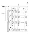
電気泳動表示装置(電気光学装置)100は、図1に示すように、素子基板2と、制御手段としてのコントローラ3と、画像データ入力回路4とを備えている。素子基板2の表面には、表示部5と、その周辺領域に走査線駆動回路6及び駆動手段としてのデータ線駆動回路7とが形成されている。これら走査線駆動回路6及びデータ線駆動回路7には、コントローラ3から直接又は画像データ入力回路4を介して制御信号や画像信号が提供されている。
[First Embodiment]
FIG. 1 shows the overall configuration of an electrophoretic display device which is an embodiment of the electro-optical device of the present invention.
As shown in FIG. 1, the electrophoretic display device (electro-optical device) 100 includes an
コントローラ3は、外部装置としてのホストコンピューターPCから供給される画像信号や同期信号に基づき、電気泳動表示装置100を総合的に制御する。ホストコンピューターPCから画像データとともに画像の書き込み指示が入力されると、その書き込み指示による入力対象の画像データを画像データ入力回路4へと出力する。
The
図2は、画像データ入力回路の構成を示す図である。
画像データ入力回路4は、1行分の画素データからなる行データの集合である画像データを入力する駆動回路であって、複数のラインメモリを有した記憶部14と、データ補正回路15とを備えている。
FIG. 2 is a diagram showing the configuration of the image data input circuit.
The image
記憶部14は、コントローラ3及びデータ補正回路15と接続されている。記憶部14は第1ラインメモリLM1、第2ラインメモリLM2、及び第3ラインメモリLM3を有しており、各ラインメモリLM1,LM2,LM3に入力対象の行データを含む連続した複数の行データを保持する。
The
データ補正回路15は、ラインメモリLM1、LM2、LM3、及びデータ線駆動回路7と接続されており、入力対象の画素データをその周囲の画素データとともに記憶部14(複数のラインメモリLM1〜LM3)から読み出し、入力対象の画素データを、周囲の画素データの情報に基づいて補正する。このデータ補正回路15は、入力対象の画像データに所定の補正を加えてデータ線駆動回路7へと転送する。
The
図3は、本実施形態に係る電気泳動表示装置100の概略構成を示す回路図である。
電気泳動表示装置100は、複数の画素40が配列された表示部5を有している。表示部5の周辺には、走査線駆動回路6およびデータ線駆動回路7が配置されている。走査線駆動回路6及びデータ線駆動回路7は、それぞれ上記コントローラ3と接続されている。
FIG. 3 is a circuit diagram showing a schematic configuration of the
The
表示部5には走査線駆動回路6から延びる複数の走査線66と、データ線駆動回路7から延びる複数のデータ線68とが形成されており、これらの交差位置に対応して画素40が設けられている。
A plurality of
走査線駆動回路6は、行方向に延びるm本の走査線66(Y1、Y2、Y3、…、Ym)を介して各々の画素40に接続されており、コントローラ3の制御のもと、1行目からm行目までの走査線66を順次選択し、画素40に設けられた選択トランジスタ41(図4参照)のオンタイミングを規定する選択信号を、選択した走査線66を介して画素40に供給する。
The scanning
データ線駆動回路7は、列方向に延びるn本のデータ線68(X1、X2、X3、…、Xn)を介して各々の画素40に接続されており、コントローラ3の制御のもと、画素40の各々に対応する画像データを規定する画像信号を画素40に供給する。
なお、本実施形態では、背景が白の場合の画像データ(画素データ)「0」(白)を規定する場合には、言い換えれば白のままにする場合には、ローレベル(L)の画像信号を画素40に供給し、画像データ(画素データ)「1」(黒)を規定する場合はハイレベル(H)の画像信号を画素40に供給する。また、中間階調の画素データを規定する場合にはLからHの中間のレベルの画像信号を画素40に供給する。
The data line driving
In this embodiment, when the image data (pixel data) “0” (white) when the background is white is defined, in other words, when it is left white, the low level (L) image is displayed. When a signal is supplied to the
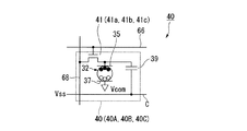
図4は、画素40の回路構成図である。
表示部5の各画素40には、選択トランジスタ41、画素電極35、電気泳動素子32(電気光学物質層)、共通電極37、及び保持容量39が設けられている。
保持容量39の一方の電極は選択トランジスタ41のドレインに接続され、他方の電極は容量線Cに接続されている。
この画素回路においては、走査線66が選択されると選択トランジスタ41がオン状態となり、データ線68から選択トランジスタ41を介して画素電極35に画像信号が入力されるとともに、保持容量39が充電される。走査線66が非選択となると選択トランジスタ41はオフ状態となるが、その後も保持容量39に蓄えられたエネルギーで電気泳動素子32の荷電粒子を移動させる。
FIG. 4 is a circuit configuration diagram of the
Each
One electrode of the
In this pixel circuit, when the
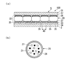
図5(a)は、表示部5における電気泳動表示装置100の部分断面図である。
電気泳動表示装置100は、素子基板2と対向基板31との間に、複数のマイクロカプセル20を配列してなる電気泳動素子32を挟持した構成を備えている。表示部5において、素子基板2の電気泳動素子32側には複数の画素電極35が配列形成されており、電気泳動素子32は接着剤層33を介して画素電極35と接着されている。
FIG. 5A is a partial cross-sectional view of the
The
素子基板2は、ガラスやプラスチック等からなる基板であり、画像表示面とは反対側に配置されるため透明なものでなくてもよい。画素電極35は、Cu箔上にニッケルめっきと金めっきとをこの順で積層したものや、Al、ITO(インジウム錫酸化物)などにより形成された電極である。図示は省略しているが、画素電極35と素子基板2との間には、図3及び図4に示した走査線66、データ線68、選択トランジスタ41などが形成されている。
The
一方、対向基板31はガラスやプラスチック等からなる基板であり、画像表示側に配置されるため透明基板とされる。対向基板31の電気泳動素子32側には複数の画素電極35と対向する平面形状の共通電極(対向電極)37が形成されており、共通電極37上に電気泳動素子32が設けられている。共通電極37は、MgAg、ITO、IZO(インジウム・亜鉛酸化物)などから形成された透明電極である。
On the other hand, the
なお、電気泳動素子32は、あらかじめ対向基板31側に形成され、接着剤層33までを含めた電気泳動シートとして取り扱われるのが一般的である。製造工程において、電気泳動シートは接着剤層33の表面に保護用の剥離シートが貼り付けられた状態で取り扱われる。そして、別途製造された素子基板2(画素電極35や各種回路などが形成されている)に対して、剥離シートを剥がした当該電気泳動シートを貼り付けることによって、表示部5を形成する。このため、接着剤層33は画素電極35側のみに存在することになる。
In general, the
図5(b)は、マイクロカプセル20の模式断面図である。
マイクロカプセル20は、例えば50μm程度の粒径を有しており、内部に分散媒21と、複数の白色粒子(電気泳動粒子)27と、複数の黒色粒子(電気泳動粒子)26とを封入した球状体である。マイクロカプセル20は、図5(a)に示すように共通電極37と画素電極35とで挟持され、1つの画素40内に1つ又は複数のマイクロカプセル20が配置される。
FIG. 5B is a schematic cross-sectional view of the
The
マイクロカプセル20の外殻部(壁膜)は、ポリメタクリル酸メチル、ポリメタクリル酸エチルなどのアクリル樹脂、ユリア樹脂、アラビアゴムなどの透光性を持つ高分子樹脂などを用いて形成される。
分散媒21は、白色粒子27と黒色粒子26とをマイクロカプセル20内に分散させる液体である。分散媒21としては、水、アルコール系溶媒(メタノール、エタノール、イソプロパノール、ブタノール、オクタノール、メチルセルソルブなど)、エステル類(酢酸エチル、酢酸ブチルなど)、ケトン類(アセトン、メチルエチルケトン、メチルイソブチルケトンなど)、脂肪族炭化水素(ぺンタン、ヘキサン、オクタンなど)、脂環式炭化水素(シクロへキサン、メチルシクロへキサンなど)、芳香族炭化水素(ベンゼン、トルエン、長鎖アルキル基を有するベンゼン類(キシレン、ヘキシルベンゼン、ヘブチルベンゼン、オクチルベンゼン、ノニルベンゼン、デシルベンゼン、ウンデシルベンゼン、ドデシルベンゼン、トリデシルベンゼン、テトラデシルベンゼンなど))、ハロゲン化炭化水素(塩化メチレン、クロロホルム、四塩化炭素、1,2−ジクロロエタンなど)、カルボン酸塩などを例示することができ、その他の油類であってもよい。これらの物質は単独又は混合物として用いることができ、さらに界面活性剤などを配合してもよい。
The outer shell (wall film) of the
The
白色粒子27は、例えば、二酸化チタン、亜鉛華、三酸化アンチモン等の白色顔料からなる粒子(高分子あるいはコロイド)であり、例えば負に帯電されて用いられる。黒色粒子26は、例えば、アニリンブラック、カーボンブラック等の黒色顔料からなる粒子(高分子あるいはコロイド)であり、例えば正に帯電されて用いられる。
これらの顔料には、必要に応じ、電解質、界面活性剤、金属石鹸、樹脂、ゴム、油、ワニス、コンパウンドなどの粒子からなる荷電制御剤、チタン系カップリング剤、アルミニウム系カップリング剤、シラン系カップリング剤等の分散剤、潤滑剤、安定化剤などを添加することができる。
また、黒色粒子26及び白色粒子27に代えて、例えば赤色、緑色、青色などの顔料を用いてもよい。かかる構成によれば、表示部5に赤色、緑色、青色などを表示することができる。
The
These pigments include electrolytes, surfactants, metal soaps, resins, rubbers, oils, varnishes, compound charge control agents, titanium-based coupling agents, aluminum-based coupling agents, silanes as necessary. A dispersant such as a system coupling agent, a lubricant, a stabilizer, and the like can be added.
Further, instead of the
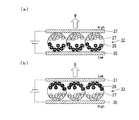
図6は、電気泳動素子の動作説明図である。図6(a)は、画素40を白表示する場合、図6(b)は、画素40を黒表示する場合をそれぞれ示している。
図6(a)に示す白表示の場合には、共通電極37が相対的に高電位、画素電極35が相対的に低電位に保持される。これにより、負に帯電した白色粒子27が共通電極37に引き寄せられる一方、正に帯電した黒色粒子26が画素電極35に引き寄せられる。その結果、表示面側となる共通電極37側からこの画素を見ると、白色(W)が認識される。
図6(b)に示す黒表示の場合、共通電極37が相対的に低電位、画素電極35が相対的に高電位に保持される。これにより、正に帯電した黒色粒子26が共通電極37に引き寄せられる一方、負に帯電した白色粒子27が画素電極35に引き寄せられる。その結果、共通電極37側からこの画素を見ると黒色(B)が認識される。
FIG. 6 is an operation explanatory diagram of the electrophoretic element. FIG. 6A shows a case where the
In the case of white display shown in FIG. 6A, the
In the case of black display shown in FIG. 6B, the
なお、図6は、黒粒子が正に、白粒子が負に帯電している場合の動作説明図であるが、必要に応じて、黒粒子を負に、白粒子を正に帯電させてもよい。この場合、上記と同様に電位を供給すると、白表示と黒表示とを反転した表示が得られる。 FIG. 6 is an operation explanatory diagram when black particles are positively charged and white particles are negatively charged. However, if necessary, black particles can be negatively charged and white particles can be positively charged. Good. In this case, when a potential is supplied in the same manner as described above, a display in which white display and black display are reversed is obtained.
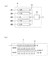
図7(a)は、画像データ入力回路4の構成を及び動作を示す図、図7(b)は、データ線駆動回路7の構成及び動作を示す図である。
画像データ入力回路4は、図7(a)に示すように複数のラインメモリLM1,LM2,LM3からなる記憶部14と、データ補正回路15とを備えている。この画像データ入力回路4は、入力対象の画素40に対応する画素データを、画像データを構成する画素データの周囲の画素データの情報に基づいて補正し、補正された画素データをデータ線駆動回路7へ供給する回路である。
FIG. 7A is a diagram showing the configuration and operation of the image
As shown in FIG. 7A, the image
記憶部14に備えられた各ラインメモリLM1,LM2,LM3は、入力対象の画像データ(すなわち表示画像)における1行分の画素データからなる行データをそれぞれ記憶するものであり、それぞれが少なくとも1行分の画素データを記憶可能な記憶容量を有している。本実施形態の場合、記憶部14は、入力対象の行データとその前後の行データの合計3行分の行データを保持する構成である。本実施形態においては、コントローラ3から出力される画像データ(連続した複数の行データ)は、データ線駆動回路7へは直接供給されず、第1ラインメモリLM1、第2ラインメモリLM2、第3ラインメモリLM3へと順番に書き込まれて保持される。
Each of the line memories LM1, LM2, and LM3 provided in the
図7(a)には、i(1≦i≦m)行目の画素データがデータ線駆動回路7に転送されるときの画像データ入力回路4の状態が示されている。第3ラインメモリLM3には入力対象の行データの1行前である(i−1)行目の行データが取り込まれており、第2ラインメモリLM2には入力対象の行データであるi行目の行データが取り込まれている。また、第1ラインメモリLM1には入力対象の行データの1行後である(i+1)行目の行データが取り込まれている。
FIG. 7A shows the state of the image
なお、i行目の次の(i+1)行目の行データをデータ線駆動回路7に転送する際には、ラインメモリLM1〜LM3には、それぞれi行目、(i+1)行目、(i+2)行目の行データが保持された状態となる。すなわち、記憶部14は、ラインメモリLM1〜LM3内で行データを順送りすることでデータ線駆動回路7に転送する行データを切り替えるとともに、この順送り動作により空いた第1ラインメモリLM1にコントローラ3から供給される新たな行データを取り込むように構成されている。
When the row data of the (i + 1) -th row after the i-th row is transferred to the data line driving
データ補正回路15は、入力対象のi行目に属する画素データをその周囲の画素データとともに記憶部14から読み出し、入力対象の画素データをその周囲の画素データの情報に基づいて補正を行い、データ線駆動回路7に転送する。具体的には、第2ラインメモリLM2に保持されているi行目の行データのうち、データ線駆動回路7に転送する画素データ(入力対象の画素データ;例えばj番地(列番号)の画素データ)とその周囲の画素データ(例えば、i行目の行データに属するj−1番地、j+1番地の画素データや、(i−1)行目及び(i+1)行目の行データに属するj−1番地、j番地、j+1番地の画素データ)を用いたブール演算の結果に基づいて補正する。
The
データ線駆動回路7は、例えば、図7(b)に示すように、シフトレジスタ17と、ラッチ回路18と、レベルシフタ19とを備えている。データ線駆動回路7は、1走査期間(走査線66の1選択期間)において、データ補正回路15から転送される補正後の画素データdを、データ線68の本数に相当するn個順次ラッチした後、ラッチしたn個の画素データdを次の走査期間においてレベルシフタ19により画像信号に変換し、それぞれに対応するデータ線68に一斉に出力するものである。
For example, as shown in FIG. 7B, the data
具体的に、図7(b)に示すデータ線駆動回路7において、シフトレジスタ17は走査期間の最初に供給されるデータイネーブル信号ENBをデータクロックCLKにしたがって転送し、ラッチ信号としてラッチ回路18に供給する。ラッチ回路18は、各画素データdに対応して2段のラッチ回路を備えた構成であり、画素データdは上記ラッチ信号にしたがって動作する1段目のラッチ回路にラッチされる。2段目のラッチ回路は、1段目のラッチ回路によりラッチされた画素データdを、データイネーブル信号ENBにしたがって一斉にラッチする。そして、2段目のラッチ回路にラッチされた画素データdが、レベルシフタ19を介して画像信号に変換され、各データ線68に供給される。
Specifically, in the data
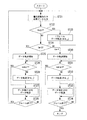
[駆動方法]
次に、電気泳動表示装置100における画像更新に係る駆動方法について説明する。本実施形態では、一例として、表示部5に「Ab」の画像を表示した後、当該画像を消去して全面白表示とし、その後に所定画像に更新する場合の駆動方法について説明する。
[Driving method]
Next, a driving method related to image update in the
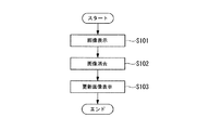
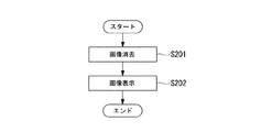
図8は、画像更新に係るフローチャート図である。
本実施形態の画像更新に係るステップは、画像表示ステップS101と、画像消去ステップS102と、更新画像表示ステップS103とを有している。
FIG. 8 is a flowchart relating to image update.
The steps relating to the image update of the present embodiment include an image display step S101, an image erasing step S102, and an updated image display step S103.
(画像表示ステップ)
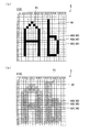
まず、画像表示ステップS101について説明する。画像表示ステップS101は、表示部5に画像を表示するステップである。具体的に、本実施形態の画像表示ステップS101では、図9(a)に示す画像P1を表示部5に表示させる。
(Image display step)
First, the image display step S101 will be described. The image display step S101 is a step of displaying an image on the
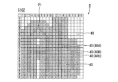
図9(a)において、画素40Aは画像P1を形成する画素40であり、画素40Bは画素40Aと隣り合って配置された背景を形成する画素40である。画素40Cは画素40Bと隣り合って配置された背景を形成する画素40であり、画素40Bに対して画素40Aと反対側に位置する画素40である。なお、図9(a)では、符号40A、40B、40Cはそれぞれ1つの画素40を指し示しているが、画素40A、40B、40Cは、上記条件を満たす複数の画素40の各々に対応する。したがって、表示部5には、それぞれ複数の画素40A、40B、40Cが含まれる。
また本実施形態の場合、画像P1が1画素幅の線画からなる文字画像であるため、画素40Aは画像P1を形成する画素であるとともに、画像P1の輪郭を形成する画素でもある。
In FIG. 9A, a
In the case of the present embodiment, since the image P1 is a character image composed of a line drawing having a width of one pixel, the
画像表示ステップS101では、少なくともデータ補正回路15は機能しない。具体的な動作を例示すると、コントローラ3から出力された画像データは、行データ毎に画像データ入力回路4に入力され、各ラインメモリLM1〜LM3に順送りされる。そして、ある行が選択されている期間内で、当該行に対応する行データ(第2ラインメモリLM2に保持されている行データ)がデータ補正回路15を介してデータ線駆動回路7に出力される。この際、データ補正回路15において演算は行われず、第2ラインメモリLM2から出力された行データがそのままデータ線駆動回路7に供給される。そして、データ線駆動回路7は、入力された行データを画像信号に変換し、データ線68を介して各画素40に供給する。なお、画像表示ステップS101では共通電極37の電位はローレベル(L;例えば0V)としてある。
In the image display step S101, at least the
画像P1の黒の絵素を形成する画素40Aでは、選択トランジスタ41aを介して、データ線68から画素電極35にハイレベル(H;例えば15V)の画像信号が入力される。一方、背景を形成する画素40B,40Cでは、それぞれ選択トランジスタ41b,41cを介して、データ線68から画素電極35にローレベル(L;例えば0V)の画像信号が入力される。
In the
ハイレベル(H)の画像信号が入力された画素40Aでは、画素電極35が相対的に高電位、共通電極37が相対的に低電位となって電気泳動素子32が黒表示動作する。これにより、図9(a)に示すような「Ab」の画像P1が表示される。一方、ローレベル(L)の画像信号が入力された画素40B,40Cでは、画素電極35と共通電極37とが同電位となるため表示は変化しない。ここでは、画像P1以外の背景部分は白表示としている。
画像P1が表示された後は、少なくとも共通電極37がハイインピーダンス状態に保持される。これにより、以降の画素40の表示状態の変更が防止され、表示画像P1が保持される。
In the
After the image P1 is displayed, at least the
(画像消去ステップ)
次に、画像消去ステップS102について説明するが、それに先立って、従来の駆動方法(反転消去)における問題点について図18及び図19を参照しつつ説明する。
図18は、画像P1を選択消去したときの表示部5の変化を示す図である。図18(a)は消去動作前の状態を示し、図18(b)は、画像P1を形成する画素40Aのみを駆動して画像P1を選択消去した後の状態を示している。
(Image deletion step)
Next, the image erasing step S102 will be described. Prior to that, problems in the conventional driving method (reverse erasing) will be described with reference to FIGS.
FIG. 18 is a diagram illustrating a change in the
図18(a)において、画像P1を形成する画素40Aのみを駆動して画像消去を実行すると、図18(b)に示すように、表示部5には画像P1の輪郭に沿った残像P2が発生する。この残像P2は、画像P1を形成する画素40Aと、これらの画素40Aと隣り合って配置され背景を構成する画素40Bとの境界付近で発生する。
In FIG. 18A, when only the
上記の残像P2は、画像P1を形成する画素40Aと、その周辺の画素40Bとを駆動して画像消去を行うことで発生を回避することができる。ここで、図19(a)は、残像P2を発生させないために設定される消去対象領域を示す図であり、図19(b)は、図19(a)に対応する輪郭消去用の画像データを示す図である。
The afterimage P2 can be avoided by erasing the image by driving the
図19(a)に示すように、残像P2を発生させずに画像P1を消去するには、画像P1を形成する画素40Aと、画素40Aと隣り合って配置され背景を構成する画素40Bとを駆動する。すなわち、画像P1だけでなくその周囲の背景の一部に対しても消去動作を実施することによって、画素40Aと画素40Bとの境界部分に位置する電気泳動素子32を駆動させ、残像P2(図18(b)参照)の発生を防止する。
しかしながら、このような消去方法を実行するためには、図19(b)に示すように、画像P1の画像データF1に、輪郭部分の画像データF2を追加した消去用の画像データを作成する必要がある。そうすると、ホストコンピューターPCやコントローラ3に、画像P1に対応する画像データを保持する第1フレームメモリの他に消去用の画像データを保持する第2フレームメモリ等を設ける必要が生じる。また、画像データ生成の演算処理によってCPUの処理時間や消費電力が増大する。
As shown in FIG. 19A, in order to erase the image P1 without generating the afterimage P2, the
However, in order to execute such an erasing method, as shown in FIG. 19B, it is necessary to create erasing image data in which the image data F1 of the contour portion is added to the image data F1 of the image P1. There is. Then, it becomes necessary to provide the host computer PC and the
これに対して本実施形態の駆動方法では、以下で説明するように、画像データ入力回路4を用いて逐次的に画像データを補正する駆動方法によって、残像を生じさせることなく画像P1の消去を行えるようにした。
On the other hand, in the driving method of the present embodiment, as will be described below, the image P1 is erased without causing an afterimage by the driving method of sequentially correcting the image data using the image
本実施形態の画像消去ステップS102において用いられる画像データは、図9(a)に示す画像P1に対応する画像データである。画像消去ステップS102に移行すると、コントローラ3から画像P1の画像データを構成する行データが画像データ入力回路4に順次出力され、ラインメモリLM1〜LM3に保持される。データ補正回路15は、入力対象の行データが保持されている第2ラインメモリLM2から画素データを読み出す際に、第1ラインメモリLM1及び第3ラインメモリLM3からも画素データを取得する。
例えば、第1ラインメモリLM1に(i+1)行目の行データが取り込まれ、第2ラインメモリLM2にi行目のデータが取り込まれ、第3ラインメモリLM3に(i−1)行目のデータが取り込まれている場合に、入力対象の画素データがi行目の行データのj番地の画素データdi,jであるとする。このとき、データ補正回路15は、上記の画素データdi,jとともに、この画素データdi,jと隣り合う画素データをもラインメモリLM1〜LM3から取得する。その後、データ補正回路15は、下記の式(1)に示すように、取得した周辺の画素データの情報(ここでは階調値)を用いたブール代数演算を実施する。
The image data used in the image erasing step S102 of the present embodiment is image data corresponding to the image P1 shown in FIG. When the process proceeds to the image erasing step S102, the row data constituting the image data of the image P1 is sequentially output from the
For example, the (i + 1) -th row data is taken into the first line memory LM1, the i-th row data is taken into the second line memory LM2, and the (i-1) -th row data is taken into the third line memory LM3. Is captured , it is assumed that the pixel data to be input is pixel data d i, j at address j in the row data of the i-th row. At this time, the
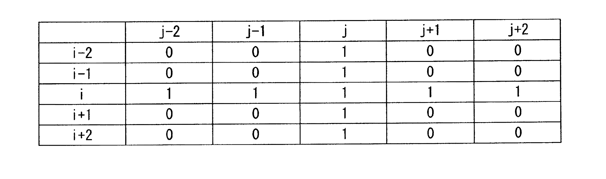
ここで、dm,nは、m行目に対応する行データのn番地の画素データであり、黒表示に対応する画素データである場合には「1」をとり、白表示に対応する画素データである場合には「0」をとる。
そして、データ補正回路15は、下記の表1に示す9入力の論理和回路で構成されており、入力対象の画素データdi,jが「1」(黒)である場合はもちろんのこと、入力対象の画素データに隣接する周辺の画素データのいずれか1つでも「1」(黒)であれば、演算結果としての入力対象の画素データdは、「1」となる。
Here, dm , n is pixel data at address n of row data corresponding to the m-th row, and is “1” when the pixel data corresponds to black display, and is a pixel corresponding to white display. When it is data, “0” is taken.
The
上記動作によりデータ補正回路15において生成された画素データdが、j番地の画素データとしてデータ線駆動回路7に送出される。データ線駆動回路7は、(i−1)行目の選択期間に、データ補正回路15から送出されるi行目の行データに対応する画素データdをシフトレジスタ17の動作によって順次ラッチ回路18(1段目)に取り込む。そして、1行分の画素データdがラッチ回路18(1段目)に取り込まれた後、走査線駆動回路6によりi行目の走査線66が選択されるタイミングで、ラッチ回路18内で1段目から2段目のラッチ回路に画素データdが一斉にラッチされる。これにより、i行目の走査線66に属する画素40の選択トランジスタ41がオン状態となる期間に、データ線駆動回路7内のラッチ回路18からレベルシフタ19を介して画像信号がデータ線68に供給され、各々の画素40に入力画素データdに応じた電位が入力される。
The pixel data d generated in the
具体的に入力される電位は、画素データdの値が「0」であれば電気泳動素子32への印加電圧を0Vとする電位が画素電極35に入力され、画素データの値が「1」であれば画素40を白表示動作させる電位が画素電極35に入力される。例えば、この画像消去ステップS102では共通電極37の電位を15Vに切り替えてあるとすると、画素データが「0」である画素40の画素電極35には15Vが入力され、画素データが「1」である画素40の画素電極35には0Vが入力される。これにより、表示部5の全ての画素40が白表示され、消去状態となる。このようにして画像P1とその輪郭の消去動作を実施する。
Specifically, if the value of the pixel data d is “0”, the potential that is applied to the
(更新画像表示ステップ)
次に、更新画像表示ステップS103に移行すると、コントローラ3により表示部5に更新画像が表示される。この更新画像表示ステップS103における具体的な動作は、先の画像表示ステップS101と同様である。すなわち、コントローラ3から出力された更新画像の画像データは、行データ毎にラインメモリLM1〜LM3に順次取り込まれる。そして、第2ラインメモリLM2に保持されている行データが、データ補正回路15によって補正されることなくデータ線駆動回路7に転送される。データ線駆動回路7は、入力された画像データから画像信号を生成し、対応するデータ線68を介して画素40に供給する。このようにして所定の更新画像が表示部5に表示される。
(Updated image display step)
Next, when the process proceeds to an update image display step S103, the
以上、詳細に説明したように、本実施形態によれば、3行分のラインメモリLM1,LM2,LM3と簡素な論理回路(9入力のOR回路)であるデータ補正回路15とを用いて、表示されている画像P1の画像データから消去用の画素データdを画像消去ステップS102の実行中に生成し、これを用いて消去動作を実行することができる。
As described above in detail, according to the present embodiment, the line memories LM1, LM2, and LM3 for three rows and the
したがって本実施形態によれば、輪郭消去用の画像データを保持するためのフレームメモリが不要となり、また、この輪郭消去用の画像データを例えばCPU等で生成しなくても良い。
よって、大規模な回路の追加やCPU負荷(処理時間、電力)がなく、迅速な輪郭消去が低消費で可能となり、残像のない高画質が得られる。
Therefore, according to the present embodiment, a frame memory for holding image data for contour erasure is not necessary, and the image data for contour erasure need not be generated by a CPU or the like, for example.
Therefore, there is no addition of a large-scale circuit or CPU load (processing time and power), and quick contour erasure can be achieved with low consumption, and high image quality without an afterimage can be obtained.
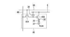
なお、本実施形態の電気泳動表示装置100において、表示部5における各画素40の画素回路の構成は上述したものに限らない。
例えば、図10に示すように、選択トランジスタ41Aと、駆動トランジスタ41Bと、画素電極35と、電気泳動素子32と、共通電極37と、保持容量39とを備え、走査線66に対応して行単位で形成された電源線Eに保持容量39と駆動トランジスタ41Bとが接続された構成であってもよい。
In the
For example, as shown in FIG. 10, a
図10において、走査線66からの制御信号に基づいて選択トランジスタ41Aをオン状態とし、データ線68からのデータ信号の電位を保持容量39に保持させる。駆動トランジスタ41Bは、保持容量39に保持されたデータ信号の電位に応じて電源線Eから電気泳動素子32に駆動電流を供給する。走査線66が非選択となっても、保持容量39により電気泳動素子32に所定の電流が供給され続ける。
In FIG. 10, the
したがって、所定の時間で選択トランジスタ41Aを再選択して保持容量39の電圧を0にすれば、電気泳動素子32への電力の供給がなくなるので、所望の表示状態で電気泳動素子32の駆動を停止させ、階調表示が可能となる。なお、図10に示す画素回路において、データ線駆動回路7から各画素40に供給される画像信号を電流信号としてもよい。すなわち、データ線駆動回路7を、電圧信号である画素データdの入力を受けて、画素データdの電圧に応じた電流をデータ線68に供給する構成としてもよい。この場合、選択トランジスタ41Aを介して保持容量39に上記電流信号が入力されることで、保持容量39が所定の電圧まで充電される。
Therefore, if the
次に、第1実施形態の変形例について以下に述べる。
(変形例1)
先に記載した第1実施形態においては、輪郭消去時の輪郭の幅を1画素としていたが、画素サイズ等によっては2画素以上が好ましいことがある。
変形例1では、図11(a)に示すように、5つのラインメモリLM1、LM2、LM3、LM4、LM5と、データ補正回路15とからなる画像データ入力回路4と、図11(b)に示すデータ線駆動回路7とを備えた構成とし、下記の式(2)を用いてブール代数和を計算する。
Next, modifications of the first embodiment will be described below.
(Modification 1)
In the first embodiment described above, the width of the contour at the time of contour erasure is one pixel, but two or more pixels may be preferable depending on the pixel size or the like.
In the first modification, as shown in FIG. 11A, an image
表2は、上記式(2)の演算を実行できるフィルタの形を示すもので、上記フィルタの値と、対応する番地の画素データの値との積のブール代数和をとる。つまり、本例におけるデータ補正回路15は、入力対象の画素データdi,jとその周囲2画素分の画素データが入力される25入力の論理和回路で構成されている。
Table 2 shows the form of a filter that can execute the operation of the above formula (2), and takes the Boolean algebra sum of the product of the filter value and the pixel data value of the corresponding address. In other words, the
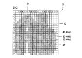
図12に、式(2)を用いて補正された画素データdに基づく消去領域を示す。
データ補正回路15は、上記のフィルタにより、画像P1の画像データ(画像P1を形成する画素40Aの画素データ)の入力を受けて、画素40Aと隣り合って配置され背景を構成する画素40Bと、画素40Bの画素40Aとは反対側で画素40Bと隣り合って配置され背景を構成する画素40bとに対して、値「1」の画素データを設定する。ここでは、画像P1に対応する画素40Aと、画素40Aの上下方向及び左右方向に並ぶ2つの画素40B,40bと、画素40Aの斜め方向に並ぶ2つ画素40B,40bに対応する画素データにより輪郭消去データ(入力対象の画像データ)が構成される。つまり、データ補正回路15は、画像P1の輪郭を2画素分外側に拡張する補正を加えた画像データを生成し、データ線駆動回路7に供給する。
データ線駆動回路7は、上記画像データの入力を受けて、各画素40A,40B,40bに対して、画素を白表示動作させる電圧あるいは電流を出力する。
FIG. 12 shows an erasing area based on the pixel data d corrected using the equation (2).
The
In response to the input of the image data, the data
また、以下に示す式(3)を用いてブール代数和を計算しても良い。 Further, the Boolean algebra sum may be calculated using the following equation (3).
ここで、表3は、上記式(3)による演算を実行できるフィルタの形を示すものである。表3に示すフィルタを備えたデータ補正回路15は、先に記載のものと同様の25入力の論理和回路であるが、入力対象の画素データdi,jから最も遠い角部に位置する画素データdi-2,j-2、di-2,j+2、di+2,j-2、di+2,j+2の4つがブール演算の対象から取り除かれている点で表2に示したフィルタと異なる。
Here, Table 3 shows the form of a filter that can execute the calculation according to the above equation (3). A
図13に、式(3)によって得られる消去用の画像データに基づく消去領域を示す。データ補正回路15は、画像P1に基づいて、画像P1の外側に配置された画素40B(画素40Aの外側に隣り合う画素40)、画素40b(画素40Bの外側に隣り合う画素40)とに、値「1」の画素データを設定する。
ここでは、画像P1に対応する画素40Aと、画素40Aの上下方向及び左右方向に配置された2つの画素40B,40bと、画素40Aの斜め方向に配置された1つ画素40Bとにより輪郭消去データが構成される。この画像データの入力を受けたデータ線駆動回路7は、消去領域を構成する画素40A、40B、40bに対して、画素を白表示動作させる電圧あるいは電流を供給する。
FIG. 13 shows an erasing area based on erasing image data obtained by Expression (3). Based on the image P1, the
Here, the contour erasure data includes the
さらに、データ補正回路15のフィルタの形は、以下の表4及び表5に示すようにしてもよい。
Further, the filter shape of the
表4に示すフィルタでは、表3において係数値「0」に設定されていた最も遠い角部の係数値を「1」とし、それらの角部に対して上下左右に隣り合う位置の係数値を「0」に設定している。表4に示すフィルタによれば、図13に示した消去用画像データの最外周部に位置する複数の画素40bが、画像P1に対応する画素40Aの輪郭に沿う方向で1つおきに配置される。
このように、消去用画像データの輪郭を形成する複数の画素40bを1画素おきに配置し、消去領域の外周端をギザギザの形状とすることにより、背景との境界が直線状とならず見えにくくなる。
In the filter shown in Table 4, the coefficient value of the farthest corner portion set to the coefficient value “0” in Table 3 is set to “1”, and the coefficient values at positions adjacent to the corner portions in the vertical and horizontal directions are set. “0” is set. According to the filter shown in Table 4, a plurality of
In this way, by arranging the plurality of
次に、表5に示すフィルタによれば、入力対象の画素データdi,jに対して、上下左右方向で2画素分の範囲にある画素データに値「1」が設定され、輪郭拡張が行われる。したがって、画像P1の輪郭に対応する画素40Aの上下方向及び左右方向に配置された2画素(画素40Bとその外側の画素40b)に対して白書き込みを行い、画素40Aの斜め方向に位置する背景領域の画素40については背景データのままの状態にする。
反転消去を行ったときの残像は、階調の異なる画素40に挟まれた境界部分に発生するため、斜め方向で階調の異なる画素40が隣り合っていたとしても、これらの画素40の境界はそれらの角部近傍のみであるため、残像が比較的生じにくい。このような場合に表5に示すフィルタを適用すれば、残像が生じやすい領域に確実に消去領域を設定しつつ、残像が生じにくい領域の画素40は消去時に駆動しないようにすることができ、電力消費が抑えられる。
Next, according to the filter shown in Table 5, the value “1” is set to the pixel data in the range of two pixels in the vertical and horizontal directions with respect to the input target pixel data d i, j , and the contour expansion is performed. Done. Therefore, white writing is performed on two pixels (
An afterimage when performing reverse erasure occurs at a boundary portion sandwiched between
(変形例2)
次に、第1実施形態の変形例2について説明する。
上記第1実施形態及び変形例1では、発明を理解しやすくするためにフィルタの係数値を「0」「1」の2値としていたが、階調表示が可能な電気泳動表示装置である場合には、データ補正回路15によって画素データの階調値を補正してデータ線駆動回路7に出力する構成とすることもできる。表6は、変形例2に係るデータ補正回路15に備えられるフィルタの形を示すものである。表6に示すフィルタを備えたデータ補正回路15は、25入力の論理和回路であり、入力対象の画素データdi,jとその周囲の画素データの階調値に、対応する番地のフィルタの係数値(wi,j)を掛けて重み付けし、これの算術和を算出したものを補正後の画素データdとして設定する(下記式(4)参照)。そして、補正された画素データdをデータ線駆動回路7に出力する。
なお、この場合にデータ線駆動回路7が、補正された画素データdに対応する電圧信号又は電流信号をデータ線68に出力可能に構成されるのはもちろんである。
(Modification 2)
Next,
In the first embodiment and the first modification, the filter coefficient values are binary values of “0” and “1” for easy understanding of the invention. However, the present invention is an electrophoretic display device capable of gradation display. Alternatively, the gradation value of the pixel data may be corrected by the
In this case, of course, the data
変形例2に係る構成によれば、入力対象の画素データdi,jを補正するに際して、その周囲の画素データの情報を参酌する程度を表6に示すフィルタにより自在に設定することができる。
例えば、入力対象の画素データdi,jから1画素分の距離に位置する画素データdi-1,j-1、di-1,i、di-1,j+1、di,j-1、di,j+1、di+1,j-1、di+1,j、di+1,j+1に対応する係数値wi-1,j-1、wi-1,i、wi-1,j+1、wi,j-1、wi,j+1、wi+1,j-1、wi+1,j、wi+1,j+1を、2画素分の距離に位置する画素データdi-2,j-2、di-2,i-1、di-2,j、di-2,j+1、di-2,j+2、di-1,j-2、di-1,j+2、di,j-2、di,i+2、di+1,j-2、di+1,j+2、di+2,j-2、di+2,j-1、di+2,j、di+2,j+1、di+2,j+2に対応する係数値wi-2,j-2、wi-2,i-1、wi-2,j、wi-2,j+1、wi-2,j+2、wi-1,j-2、wi-1,j+2、wi,j-2、wi,i+2、wi+1,j-2、wi+1,j+2、wi+2,j-2、wi+2,j-1、wi+2,j、wi+2,j+1、wi+2,j+2の2倍に設定し、入力対象の画素データdi,jと隣り合う画素の情報の貢献度を高く設定することもできる。
According to the configuration according to the modification example 2, when the pixel data di, j to be input is corrected, the degree of reference to the information of the surrounding pixel data can be freely set by the filter shown in Table 6.
For example, pixel data d i−1, j−1 , d i−1, i , d i−1, j + 1 , d i, d located at a distance of one pixel from the input target pixel data d i, j . Coefficient values w i−1, j−1 , w corresponding to j−1 , d i, j + 1 , d i + 1, j−1 , d i + 1, j , d i + 1, j + 1 i-1, i , wi -1, j + 1 , wi , j-1 , wi , j + 1 , wi + 1, j-1 , wi + 1, j , wi + 1, j + 1 is pixel data d i-2, j-2 , d i-2, i-1 , d i-2, j , d i-2, j + 1 , d located at a distance of two pixels. i-2, j + 2 , d i-1, j-2 , d i-1, j + 2 , d i, j-2 , d i, i + 2 , d i + 1, j-2 , d i + 1, j + 2 , d i + 2, j-2 , d i + 2, j-1 , d i + 2, j , d i + 2, j + 1 , d i + 2, j + 2 Coefficient values w i-2, j-2 , w i-2, i-1 , w i-2, j , w i-2, j + 1 , w i-2, j + 2 , w i -1, j-2, w i -1, j + 2, w i, j-2, w i, i + 2, w i + 1, j-2, w i + 1, j + 2, w i + 2, j-2 , wi + 2, j-1 , wi + 2, j , wi + 2, j + 1 , wi + 2, j + 2 pixel data d i, higher set the contribution of information of the pixel adjacent to the j It is also possible to.
また、図13に示した画素40のうち、元々白表示されている背景領域に位置する画素40Bや画素40bに対応する画素データdが中間階調値となるようにすれば、画像P1を構成する画素40Aにおいて黒表示を白表示に書き換える消去駆動を実行する一方で、画素40B、40bにおいて画素40Aよりも弱い白書き込みとすることができる。これにより、白背景部分にさらに白書き込みを行うことによる電気泳動素子32の電流履歴の偏りを抑制することができ、信頼性の低下を防止することができる。
なお、変形例2では5行5列の画素データを用いて入力対象の画素データの補正を行うこととしたが、これに限定されるものではなく、必要に応じて行数及び列数を増減することができる。
Further, if the pixel data d corresponding to the
In the second modification, the pixel data to be input is corrected using the pixel data of 5 rows and 5 columns. However, the present invention is not limited to this, and the number of rows and the number of columns may be increased or decreased as necessary. can do.
[第2実施形態]
次に、本発明の第2実施形態について説明する。なお、第1実施形態と同一の構成要素については、その説明を省略する。
[Second Embodiment]
Next, a second embodiment of the present invention will be described. Note that the description of the same components as those in the first embodiment is omitted.
まず、複数の画像を表示部5に表示させる場合の問題点について説明する。
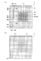
図14(a)は、複数の画像P11〜P13を表示させたときの表示部5の状態を示す図である。図14(b)は、複数の画像P11〜P13に対応する画像データ(フレームメモリに展開された状態)を示す図である。なお、図14(b)では黒表示に対応する画素データの値を「1」とする一方、白表示の画素データ(「0」)は省略して空白にしてある。
First, problems when displaying a plurality of images on the
FIG. 14A is a diagram illustrating a state of the
図14(b)に示すように、表示部5に表示される画像P11〜P13の画像データD11〜D13は、いずれも黒表示に対応する値「1」の画素データ及びその集合により構成される。画像P11は9×9画素の正方形状の画像であり、画像P12は9×1画素の直線状の画像であり、画像P13は1画素のドット状の画像である。
As shown in FIG. 14B, the image data D11 to D13 of the images P11 to P13 displayed on the
電気泳動表示装置100において、上記の画像P11、P12,P13を、画像データD11〜D13をそのまま用いて表示部5に表示させると、図14(a)に示すように、各画像P11、P12,P13を構成する画素40の画素電極35に対して同一の電圧を印加したとしても、画素40の場所によって表示色が異なってしまうという不具合が生じる。
具体的には、画像P11では、輪郭部分に位置する1画素幅の枠状領域を構成する画素40cの表示色が、内側に配置された画素40sよりも薄い黒色(グレー)になってしまう。また、画像P12では、全体が画像P11の画素40cよりも薄いグレー表示となり、そのうちでも両端の画素40dが、内側の画素40eよりも薄いグレー表示になる。また、単一の画素40fからなる画像P13では、画像P12の画素40dよりもさらに薄いグレー表示になる。
つまり、複数の画素40に対して同じ黒にする電圧を印加したとしても、その周りを取り囲む白色の画素40Bの個数が多くなるほど(黒の画素が孤立するほど)表示色が白に近いグレー表示になる。
In the
Specifically, in the image P11, the display color of the
In other words, even when the same black voltage is applied to the plurality of
これを解消するためには、表示が2値表示であってもフレームメモリを多bit化して上記の黒さの変化を補償するデータを保管し、その数値にあわせて黒表示時に画素電極35に印加される電圧を補正すればよいが、フレームメモリが大型化してしまう。また、補正計算を行うためCPUの負担が大きくなる。
In order to solve this, even if the display is binary display, the frame memory is made multi-bit to store the data to compensate for the change in blackness, and in accordance with the numerical value, the data is stored in the
そこで、本実施形態の電気泳動表示装置では、画像データ入力回路4において画像データを補正し、この補正された画像データを用いて表示を行うことで、画像P11、P12,P13のいずれにおいても表示むらの発生を防止できるようにした。以下、本実施形態の電気泳動表示装置とその駆動方法について、図面を参照しつつ詳細に説明する。
Therefore, in the electrophoretic display device according to the present embodiment, the image
図15は、本実施形態の電気泳動表示装置200の概略構成図である。
図15に示すように、電気泳動表示装置200は、画像データ入力回路204を備えている。画像データ入力回路204は、3つのラインメモリLM1〜LM3からなる記憶部14と、記憶部14と接続されたデータ補正回路215とを備えている。データ補正回路215は、データ線駆動回路7及びコントローラ3と接続されており、コントローラ3からは書込回数Cwが入力される。
FIG. 15 is a schematic configuration diagram of the
As shown in FIG. 15, the
表7に、本実施形態におけるデータ補正回路215の演算処理で用いられるフィルタの形を示す。このフィルタを備えたデータ補正回路215は9入力の論理和回路であり、表7のフィルタによって抽出された画素データの算術和sumを計算する。そして、sumの値に基づいて入力対象の画素データdi,jを補正し、補正された画素データdとしてデータ線駆動回路7に出力する。
詳細は後述するが、データ補正回路215は、コントローラ3から入力される書込回数Cwの値と、算術和sumの値とに基づいて異なる動作を実行する。
Table 7 shows the shape of the filter used in the arithmetic processing of the
Although details will be described later, the
図14に示した表示むらは、表示部5に画像を表示させる際に発生するものであるから、データ補正回路215は表示部5に画像データに基づく画像を表示させる際に、画像データを補正する回路として機能する。
Since the display unevenness shown in FIG. 14 occurs when an image is displayed on the
以下、電気泳動表示装置200及び画像データ入力回路204の動作について、詳細に説明する。
図16は、本実施形態の電気泳動表示装置200の駆動方法を示すフローチャートであり、図17は、データ補正回路215の動作を示すフローチャートである。
Hereinafter, operations of the
FIG. 16 is a flowchart showing a driving method of the
以下に説明する本実施形態の電気泳動表示装置200の駆動方法では、図16に示すように、表示部5を全面白表示させて消去状態とする画像消去ステップS201と、全面白表示の表示部5に対して黒色画像を表示させる画像表示ステップS202とを実行する。また本実施形態の場合、画像表示ステップS202を4フレームで完了させる。すなわち、画像表示ステップにおいて、各行の走査線66を選択して画素40に所定の画像信号を入力し保持容量39を充電する動作を4回行う。
In the driving method of the
まず、画像消去ステップS201において、表示部5を全白消去する。画像消去ステップS201における具体的動作に限定はなく、白表示に対応する値「0」の画素データのみからなる画像データを用いて画像表示動作を行うことで表示部5の全面を白表示に移行させてもよいし、表示部5に何らかの画像が表示されている場合には、先の第1実施形態及び変形例に係る画像消去ステップS102を実行してもよい。
First, in the image erasing step S201, the
表示部5が全白消去されたならば、画像表示ステップS202に移行する。
画像表示ステップS202では、例えば図14(a)に示すような複数の画像P11,P12,P13に対応する画像データ(図14(b)参照)を用いて、表示部5に4回の画像書き込み動作が行われる。このとき、画像P11〜P13の画像データは、画像データ入力回路204を経由してデータ線駆動回路7に供給されるが、画像データ入力回路204のデータ補正回路215は、図15に示すように、コントローラ3から記憶部14を介して入力される画素データ(算術和sum)と、コントローラ3から入力される書込回数Cwとに基づいて異なる動作を実行する。
If the
In the image display step S202, for example, image data is written four times on the
画像表示ステップS202において、表示に供される画像データは、コントローラ3から画像データ入力回路204のラインメモリLM1〜LM3に行毎に取り込まれる。この動作は先の第1実施形態の画像データ入力回路4と同様である。
データ補正回路215では、第2ラインメモリLM2に入力対象のi行目の行データの入力が入力されたタイミングで、図17に示すステップST21が開始される。ステップST21において、データ補正回路215には、コントローラ3から書込回数Cw(=1)が入力され、ラインメモリLM1〜LM3から入力対象の画素データdi,jが順次入力される。
In the image display step S202, the image data to be displayed is fetched from the
In the
次いで、ステップST22において、書込回数Cwの値が評価され、書込回数Cwが2回以下であればステップST23へ移行し、それ以外であればステップST24に移行する。ここでは、書込回数Cw=1であるため、ステップST23へ移行する。ステップST23では、画素データの補正を行うことなくデータ補正回路215からデータ線駆動回路7へ、1フレーム分の画素データd(=di,j)の出力が行われる。つまり、1フレーム目の書き込みにおいてデータ補正回路215のデータ補正機能は動作せず、コントローラ3から供給される画像データがそのままデータ線駆動回路7に転送される。
Next, in step ST22, the value of the write count Cw is evaluated, and if the write count Cw is 2 or less, the process proceeds to step ST23, and otherwise, the process proceeds to step ST24. Here, since the write count Cw = 1, the process proceeds to step ST23. In step ST23, pixel data d (= d i, j ) for one frame is output from the
上記の1フレーム目の画像書き込みに対応するステップST23が終了したならば、ステップST21に戻り、2フレーム目の画像書き込みが開始される。このときのステップST21では、コントローラ3から入力される書込回数Cw=2であるため、続くステップST22では、1フレーム目と同様にステップST23への移行が選択される。そして、ステップST23において、データ補正回路215は、コントローラ3から供給される画像データを補正することなく1フレーム分の画像データがデータ線駆動回路7に転送される。
このように、本実施形態の駆動方法では、2フレーム目までは、コントローラ3から供給される画像データをそのままデータ線駆動回路7に供給し、表示部5への画像表示動作を行う。
When step ST23 corresponding to the image writing of the first frame is completed, the process returns to step ST21 and image writing of the second frame is started. In step ST21 at this time, since the write count Cw = 2 input from the
As described above, in the driving method of the present embodiment, the image data supplied from the
上記の2フレーム目の画像書き込みが終了したならば、再びステップST21に戻り、3フレーム目の画像書き込みが開始される。このときのステップST21では、コントローラ3から入力される書込回数Cw=3であるため、ステップST22を経由してステップST24に移行し、さらにステップST25に移行する。ステップST25においてデータ線駆動回路7へのデータ転送動作が開始されると、まず、ステップST26において表7に示したフィルタを用いて抽出した画素データの算術和sumが算出され、評価される。
When the image writing for the second frame is completed, the process returns to step ST21 again, and image writing for the third frame is started. In step ST21 at this time, since the write count Cw input from the
具体的に、ステップST26では、入力対象の画素データdi,jの周囲に配置された8画素分の画素データの値(「0」又は「1」)の合計がsumとして算出される。したがって、sumの範囲は0以上8以下の整数となる。
ステップST26におけるsumの値評価において、sumの値が7以上である場合(すなわち、入力対象の画素データdi,jの周囲の7画素以上が黒表示に対応する画素データである場合)には、ステップST27に移行する。そして、ステップST27において入力対象の画素データdi,jは破棄され、補正後の画素データd=0がデータ線駆動回路7に供給される。つまり、周囲に黒表示の画素40が多数配置されている画素40では3回目の書き込みは行われないことになる。
一方、sumの値が7未満である場合には、ステップST28に移行する。ステップST28では、入力対象の画素データdi,jを補正することなくそのまま画素データdとしてデータ線駆動回路7に供給する。つまり、周囲に黒表示の画素40が比較的少ない(0以上6個以下である)場合には、3回目の黒書き込みが行われることになる。
Specifically, in step ST26, the sum of pixel data values (“0” or “1”) for eight pixels arranged around the pixel data d i, j to be input is calculated as sum. Therefore, the range of sum is an integer of 0 or more and 8 or less.
In the sum value evaluation in step ST26, when the sum value is 7 or more (that is, when 7 or more pixels around the pixel data d i, j to be input are pixel data corresponding to black display). The process proceeds to step ST27. In step ST27, the pixel data d i, j to be input is discarded, and the corrected pixel data d = 0 is supplied to the data line driving
On the other hand, when the sum value is less than 7, the process proceeds to step ST28. In step ST28, the pixel data d i, j to be input is supplied as it is to the data line driving
上記のステップST27又はステップST28の実行後、ステップST29において、1フレーム分のデータ転送が終了したか否かが評価され、データ転送が終了していない場合には、次の画素データdi,jについてステップST26〜ST28が実行される。1フレーム分のデータ転送が終了している場合には、3フレーム目の画像書き込みを終了し、ステップST21に戻る。 After executing step ST27 or step ST28, it is evaluated in step ST29 whether or not the data transfer for one frame has been completed. If the data transfer has not been completed, the next pixel data d i, j Steps ST26 to ST28 are executed. If the data transfer for one frame has been completed, the image writing for the third frame is terminated, and the process returns to step ST21.
その後、4フレーム目の画像書き込みが開始される。このときのステップST21では、コントローラ3から入力される書込回数Cw=4であるため、ステップST22を経由してステップST24に移行し、さらにステップST30に移行する。ステップST30においてデータ線駆動回路7へのデータ転送動作が開始されると、まず、ステップST31において画素データの算術和sumが算出され、評価される。
Thereafter, image writing for the fourth frame is started. In step ST21 at this time, since the write count Cw = 4 input from the
ステップST31におけるsumの値評価において、sumの値が3以上である場合(すなわち、入力対象の画素データdi,jの周囲の3画素以上が黒表示に対応する画素データである場合)には、ステップST32に移行する。そして、ステップST32において入力対象の画素データdi,jは破棄され、補正後の画素データd=0がデータ線駆動回路7に供給される。つまり、周囲に黒表示の画素40が3個以上配置されている画素40では4回目の書き込みは行われないことになる。
一方、sumの値が3未満である場合には、ステップST33に移行する。ステップST33では、入力対象の画素データdi,jを補正することなくそのまま画素データdとしてデータ線駆動回路7に供給する。つまり、周囲に黒表示の画素40が0〜2個のみ配置されている場合には、4回目の黒書き込みが行われることになる。
In the sum value evaluation in step ST31, when the sum value is 3 or more (that is, when 3 or more pixels around the pixel data d i, j to be input are pixel data corresponding to black display). The process proceeds to step ST32. In step ST32, the pixel data d i, j to be input is discarded, and the corrected pixel data d = 0 is supplied to the data line driving
On the other hand, when the sum value is less than 3, the process proceeds to step ST33. In step ST33, the pixel data d i, j to be input is supplied as it is to the data line driving
上記のステップST32又はステップST33の実行後、ステップST34において、1フレーム分のデータ転送が終了したか否かが評価され、データ転送が終了していない場合には、次の画素データdi,jについてステップST31〜ST33が実行される。1フレーム分のデータ転送が終了している場合には、画像表示ステップS202が終了する。 After execution of step ST32 or step ST33, it is evaluated in step ST34 whether or not the data transfer for one frame has been completed. If the data transfer has not been completed, the next pixel data d i, j Steps ST31 to ST33 are executed. If the data transfer for one frame has been completed, the image display step S202 ends.
このように本実施形態では、入力対象の画素データdi,jの周囲に黒表示に対応する画素データが多く存在する場合は、入力対象の画素に対して2回の書き込みが行われ、中程度では3回の書き込みが行われ、入力対象の画素に対応する画素データの周囲に白表示に対応する画素データが多く存在し、黒表示に対応する画素データが少ない場合は、4回の書き込みが行われる。 As described above, in the present embodiment, when there is a large amount of pixel data corresponding to black display around the pixel data d i, j to be input, writing is performed twice for the pixel to be input. If the pixel data corresponding to the input target pixel has a lot of pixel data corresponding to the white display and the pixel data corresponding to the black display is small, the writing is performed four times. Is done.
本実施形態で示した具体例における周囲の黒データ数(黒表示に対応する画素データの個数)と書込回数との関係を表8に示す。本実施形態では、全ての入力対象の画素に対して少なくとも2回の書き込みを行い、周囲の黒データ数が3〜6個の画素データでは3回、周囲の黒データ数が7個又は8個の画素データでは4回の書き込みを行う。
なお、周囲の黒データ数と書込回数の関係は、一例を示したに過ぎず、表示むらの程度に応じて適宜設定することができる。
Table 8 shows the relationship between the number of surrounding black data (the number of pixel data corresponding to black display) and the number of writings in the specific example shown in the present embodiment. In the present embodiment, writing is performed at least twice for all input target pixels, and the number of surrounding black data is 3 or 3 for pixel data having 3 to 6 surrounding black data, and the number of surrounding black data is 7 or 8. For the pixel data, writing is performed four times.
The relationship between the number of surrounding black data and the number of writings is merely an example, and can be set as appropriate according to the degree of display unevenness.
以上詳細に説明したように、第2実施形態に係る電気泳動表示装置及びその駆動方法によれば、周囲に黒表示の画素が少ない孤立した画素の表示が薄くなるといった表示むらを解消することができ、均一な濃さの表示画像が得られる。また、入力対象の画素全てに対して必要以上の書き込みを行うことがないので、電力の消費が抑えられる。 As described above in detail, according to the electrophoretic display device and the driving method thereof according to the second embodiment, it is possible to eliminate display unevenness such as the display of an isolated pixel having a small number of black display pixels in the surrounding area becomes thin. And a display image with uniform darkness can be obtained. In addition, since unnecessary writing is not performed on all input target pixels, power consumption can be suppressed.
(変形例)
次に、第2実施形態の変形例について説明する。
上記第2実施形態では、周囲の黒データ数に応じて画素40を駆動する回数(書込回数)を調整することで、表示むらを解消するものとしたが、階調表示が可能な電気泳動表示装置である場合には、データ補正回路215によって画素データの階調値を補正してデータ線駆動回路7に出力する構成とすることもできる。
(Modification)
Next, a modification of the second embodiment will be described.
In the second embodiment, the display unevenness is eliminated by adjusting the number of times the
表9は、変形例に係るデータ補正回路215に備えられるフィルタの形を示すものである。表9に示すフィルタを備えたデータ補正回路215は、9入力の論理和回路であり、入力対象の画素データdi,jとその周囲の画素データの階調値に、対応する番地のフィルタの係数値(wi,j)を掛けて重み付けし、これの算術和を算出したものを補正後の画素データdとして設定する(下記式(5)参照)。そして、補正された画素データdをデータ線駆動回路7に出力する。
なお、この場合にデータ線駆動回路7が、補正された画素データdに対応する電圧信号又は電流信号をデータ線68に出力可能に構成されるのはもちろんである。また表6に示した5行5列単位に限定するものではなく、必要に応じて行数及び列数を増減してもよい。
Table 9 shows the shape of the filter provided in the
In this case, of course, the data
例えば、表10に示すように、図14に示した画像P11,P12,P13を形成する画素40のうち、表示が薄くなる画素40c〜40fに対する画素データの階調値を補正することができる。
図14に示したように、画素40c〜40fは、周囲に配置された黒表示の画素40の個数が少ないものほど黒表示が薄くなる。そこで、表10に示すように、周囲の黒表示の画素40の個数に応じて、最も濃い黒表示が得られる画素40sの階調値に対して1.2〜1.5倍とする。これにより、画素40c〜40fにおいて、電気泳動素子32に印加する電圧ないし入力する電流を画素40sによりも多くすることができ、黒表示が薄くなるのを防止することができる。
For example, as shown in Table 10, it is possible to correct the gradation value of the pixel data for the
As shown in FIG. 14, in the
以上、添付図面を参照しながら本発明に係る好適な実施形態について説明したが、本発明は係る例に限定されないことは言うまでもない。当業者であれば、特許請求の範囲に記載された技術的思想の範疇内において、各種の変更例または修正例に想到し得ることは明らかであり、それらについても当然に本発明の技術的範囲に属するものと了解される。 As described above, the preferred embodiments according to the present invention have been described with reference to the accompanying drawings, but the present invention is not limited to the examples. It is obvious for those skilled in the art that various changes or modifications can be conceived within the scope of the technical idea described in the claims. It is understood that it belongs to.
例えば、先の記載の画像データ入力回路4,204(ラインメモリLM1〜3及びデータ補正回路15,215)をコントローラ3又はデータ線駆動回路7に内蔵することもできる。
また、上記各実施形態では、記憶部14がラインメモリである場合について説明したが、1フレーム分の画像データを保持するフレームメモリであってもよい。本発明の場合、元の画像データは変更せず、データ補正回路15,215を介してデータ線駆動回路7に転送する際に、画素データの生成や変更を行うため、表示用の画像データを保持するフレームメモリからデータ補正回路15,215に画素データを直接供給してもよい。
特に書き込みあるいは消去を複数回実行する場合に、上位装置から画像データを転送せずに済むので、消費電力が抑えられ、上位装置内のCPUの処理時間も省くことができる。
For example, the above-described image
In the above embodiments, the case where the
In particular, when writing or erasing is performed a plurality of times, it is not necessary to transfer image data from the host device, so that power consumption can be suppressed and processing time of the CPU in the host device can be saved.
[第3実施形態]
次に、本発明の第3実施形態について説明する。
図20は、本発明の電気光学装置の一実施例である電子ブックリーダーの外観図、図21は、電子ブックリーダーの内部構成を示す図である。
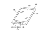
図20に示すように、電子ブックリーダー300は、筐体101と、筐体101の一方の面に形成された矩形状の開口部101aに装着された電気泳動表示パネル119とを備えている。筐体101には、ページ送りボタン105と、ページ戻しボタン106と、決定ボタン108と、スキップ送りボタン115と、スキップ戻しボタン116と、が設けられている。
[Third Embodiment]
Next, a third embodiment of the present invention will be described.
FIG. 20 is an external view of an electronic book reader which is an embodiment of the electro-optical device of the present invention, and FIG. 21 is a diagram illustrating an internal configuration of the electronic book reader.
As shown in FIG. 20, the
ページ送りボタン105は、電気泳動表示パネル119に現在表示されているドキュメント(画像)の次ページ以降を、1回押される毎に1ページずつ送って表示させる機能を起動する操作部である。ページ戻しボタン106はドキュメントの前ページ以前を、1回押される毎に1ページずつさかのぼって表示させる機能を起動する操作部である。
スキップ送りボタン115は、1回押される毎に、例えば10ページ先のページを表示させる機能を起動する操作部である。スキップ戻しボタン116は、1回押される毎に、例えば10ページ前のページを表示させる機能を起動する操作部である。スキップ送りボタン115及びスキップ戻しボタン116のページスキップ数は任意に設定することができる。
The
The
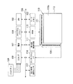
電子ブックリーダー300は、図21に示すように、CPU(Central Processing Unit )102、ワークメモリ(RAM(Random Access Memory))103、プログラムメモリ(ROM(Read Only Memory))104、入力I/F109、VRAM(Video RAM)110、表示部制御回路(コントローラー)111、電気泳動表示パネル119、タッチパネルI/F114、電源107、及び表示部用温度センサ117を備えており、各部はバス118を介して信号を授受可能に接続されている。
As shown in FIG. 21, the
また、入力I/F109には、入力ボタン130が接続されている。入力ボタン130は、図20に示したページ送りボタン105、ページ戻しボタン106、スキップ送りボタン115及び決定ボタン108を含む。タッチパネルI/F114には、タッチパネル113が接続されている。さらに、表示部制御回路111には、電気泳動表示パネル119に備えられた走査線駆動回路120とデータ線駆動回路121とが接続されている。
An
CPU102は、プログラムメモリ104に格納された基本制御プログラムやアプリケーションプログラム等の各種プログラム及びデータを読み込み、それら各種プログラム及びデータをワークメモリ103内に設けられるワークエリアに展開実行して、電子ブックリーダーが備える各部の制御を実行する。
また、CPU102は、入力I/F109から後述するページ送り信号が出力されていると、電気泳動表示パネル119に表示されているドキュメントの次ページに対応する画像データ(以下、ラスタデータとも呼ぶ。)を生成し、そのラスタデータをVRAM110に格納する。
The
Further, the
さらに、CPU102は、入力I/F109から後述するページ戻し信号が出力されていると、電気泳動表示パネル119に表示されているドキュメントの前ページに対応するラスタデータを生成し、そのラスタデータをVRAM110に格納する。また、入力I/F109から後述する連続送り信号が出力されていると、電気泳動表示パネル119に表示されているドキュメントの次ページ以降に対応するラスタデータを次々と生成し、そのラスタデータをVRAM110に次々と格納する。
Further, when a page return signal described later is output from the input I /
さらに、CPU102は、入力ボタン130(ページ送りボタン105、ページ戻しボタン106、スキップ送りボタン115及び決定ボタン108のいずれか)が押下操作されるたびに、後述する表示可能ページ数表示処理を実行し、現在の駆動用電池の残量で表示可能なページ数(表示可能ページ数)を示す画像のラスタデータを生成し、そのラスタデータをVRAM110に格納する。
Furthermore, every time the input button 130 (any one of the
ワークメモリ103は、CPU102が各種プログラムに従って上記処理を実行するときに、各種プログラムを展開するワークエリアを形成するとともに、CPU102により実行される各種処理に係るデータを展開するためのメモリ領域を形成する。
なお、ワークメモリ103としては、FeRAM(Ferroelectric Random Access Memory)やMRAM(Magnetoresistive random access memory)等の不揮発性メモリを使用する。
ワークメモリ103として不揮発メモリを使用することで、利用者によるコンテンツの閲覧時間に関わらず、1ページ分のコンテンツの表示に消費されるワークメモリ103の消費電力を一定とすることができ、表示可能ページ数を容易かつ正確に算出することができる。これに対してワークメモリ103として駆動用電池の電力を消費するDRAM(Dynamic Random Access Memory)等の揮発性メモリを使用する方法では、コンテンツの閲覧時間に応じてワークメモリ103の消費電力が変化してしまい、表示可能ページ数を精度よく算出することが困難となる。
The
As the
By using a non-volatile memory as the
プログラムメモリ104は、CPU102により実行される基本制御プログラム、各種アプリケーションプログラム及びこれら各プログラムに係るデータ等を格納する。そして、CPU102からの読み出し要求に従って、それら各種プログラムやデータをCPU102に出力する。
なお、プログラムメモリ104内の各種プログラム及びデータは、いずれもCPU102により読み取り及び実行可能な形式で格納されている。
The
Various programs and data in the
入力I/F109には、入力ボタン130として、次ページの画像を電気泳動表示パネル119に切換表示させるためのページ送りボタン105、前ページの画像を電気泳動表示パネル119に切換表示させるためのページ戻しボタン106、次ページのコンテンツを電気泳動表示パネル119に次々と切換表示させるためのスキップ送りボタン115、及び決定ボタン108が接続されている。入力I/F109は、ページ送りボタン105が押下操作されるとページ送り信号をCPU102に出力する。また、ページ戻しボタン106が押下操作されるとページ戻し信号をCPU102に出力し、スキップ送りボタン115が押下操作されると連続送り信号をCPU102に出力する。
In the input I /
VRAM110は、CPU102からの書き込み要求に従ってページごとの画像のラスタデータを格納する。また、格納したラスタデータを、表示部制御回路111からのデータ送出要求に従ってデータ線駆動回路121に出力する。表示部制御回路111は、VRAM110に格納されているラスタデータを電気泳動表示パネル119に表示させるための各種制御信号を生成し、走査線駆動回路120及びデータ線駆動回路121に供給する。
The
電気泳動表示パネル119は、複数の画素がアレイ状に形成された電気泳動表示パネル119、つまり電力の供給を止めてもそれまでの表示内容を保持可能な電気泳動素子を具備したパネルを有する。電気泳動表示パネル119は、画素形成領域(表示領域)119aの一辺端部に沿って設けられた走査線駆動回路120と、画素形成領域119aの他の一辺端部に沿って設けられたデータ線駆動回路121とを備えている。
The
走査線駆動回路120は、表示部制御回路111から出力される制御信号に基づいて複数の画素に選択信号を入力する。データ線駆動回路121は、表示部制御回路111から出力される制御信号に基づいて、走査線駆動回路120から選択信号を入力された画素にVRAM110から出力されるラスタデータを入力する。これにより、電気泳動表示パネル119に、VRAM110に保持されたページの画像を表示することができる。
The scanning
なお、本実施形態では走査線駆動回路120とデータ線駆動回路121とを備えたアクティブマトリクス方式の電気泳動表示パネル119を示しているが、電気泳動表示パネル119としてはセグメント駆動方式の電気泳動表示パネルであってもよい。また、走査線駆動回路120及びデータ線駆動回路121以外の駆動回路(共通電極駆動回路等)が設けられ、表示部制御回路111に接続されている構成であってもよい。
In this embodiment, an active matrix type
タッチパネルI/F114には、電気泳動表示パネル119の前面側(表示面側)に配設されたタッチパネル113が接続されている。そして、タッチパネル113が押圧操作されると操作位置を示すタッチパネル信号をCPU102に出力する。タッチパネル113としては任意の方式のものを用いることができる。すなわち、抵抗膜方式や静電容量方式のタッチパネルを用いることができる。
A
表示部用温度センサ117は、電気泳動表示パネル119の温度を検出し、検出された温度をCPU102に出力する。表示部用温度センサ117としては例えばサーミスタを使用し、その出力電圧を測定することで電気泳動表示パネル119の温度を検出する。表示部用温度センサ117で検出された温度は、後述する表示可能ページ数の算出において使用される。
The display
図22は、表示部制御回路の内部構成を示す図である。
表示部制御回路111は、全体制御部140と、画像データ書込制御部141と、タイミング信号生成部142と、記憶装置制御部144と、画像データ読出制御部145と、画像信号生成部146と、選択信号生成部147とを有してなり、このような表示部制御回路111には電気泳動表示パネル119が接続されている。電気泳動表示パネル119は、電気泳動素子を備えた表示部150、走査線駆動回路120、およびデータ線駆動回路121を備えている。
FIG. 22 is a diagram illustrating an internal configuration of the display unit control circuit.
The display
全体制御部140には、画像データ書込制御部141と、タイミング信号生成部142とが接続されている。画像データ書込制御部141には記憶装置制御部144が接続されている。タイミング信号生成部142には画像データ読出制御部145と画像信号生成部146と選択信号生成部147とが接続されている。
An image data write
表示部制御回路111は、全体制御部140においてCPU102と接続され、画像信号生成部146及び選択信号生成部147において電気泳動表示パネル119と接続され、記憶装置制御部144においてVRAM110と接続されている。
The display
以上に説明した電子ブックリーダー300では、電気泳動表示パネル119を構成する走査線駆動回路120及びデータ線駆動回路121が形成された素子基板上に、CPU102、ワークメモリ103、プログラムメモリ104、入力I/F109、VRAM110、表示部制御回路111、タッチパネルI/F114、電源107、及び表示部用温度センサ117が形成されており、1つの基板上に電気泳動表示パネル119に画像を表示させるために必要な回路要素をまとめて実装することで1チップ化を実現することができた。
従来の構成では、電気泳動表示パネル119に対して画像データに基づく画像信号を供給する走査線駆動回路120およびデータ線駆動回路121と、これら駆動回路120,121を駆動するCPU102や表示部制御回路111等とは別チップあるいは単品で構成されることが多かったが、本実施形態ではこれらを同一基板上に実装させることで複数の単独チップを1チップ化することができ、省スペース化を実現することができた。また、1チップに集約化することで、従来よりも大幅なコスト削減及び低消費電力化を図ることが可能である。
In the
In the conventional configuration, a scanning
(電子機器)
次に、上記各実施形態の電気泳動表示装置100を、電子機器に適用した場合について説明する。
図23は電子ペーパー1100の構成を示す斜視図である。電子ペーパー1100は、上記実施形態の電気泳動表示装置100を表示領域1101に備えている。電子ペーパー1100は可撓性を有し、従来の紙と同様の質感及び柔軟性を有する書き換え可能なシートからなる本体1102を備えて構成されている。
(Electronics)
Next, a case where the
FIG. 23 is a perspective view illustrating a configuration of the
図24は、電子ノート1200の構成を示す斜視図である。電子ノート1200は、上記の電子ペーパー1100が複数枚束ねられ、カバー1201に挟まれているものである。カバー1201は、例えば外部の装置から送られる表示データを入力する図示は省略の表示データ入力手段を備える。これにより、その表示データに応じて、電子ペーパーが束ねられた状態のまま、表示内容の変更や更新を行うことができる。
FIG. 24 is a perspective view showing the configuration of the
以上の電子ペーパー1100、及び電子ノート1200によれば、本発明に係る電気泳動表示装置が採用されているので、簡素な構造で容易にリセット動作可能に構成された光書き込み型の表示手段を備えた電子機器となる。
According to the
なお、上記の電子機器は、本発明に係る電子機器を例示するものであって、本発明の技術範囲を限定するものではない。例えば、携帯電話、携帯用オーディオ機器などの電子機器の表示部にも、本発明に係る電気泳動表示装置は好適に用いることができる。 In addition, said electronic device illustrates the electronic device which concerns on this invention, Comprising: The technical scope of this invention is not limited. For example, the electrophoretic display device according to the present invention can be suitably used for a display portion of an electronic device such as a mobile phone or a portable audio device.
100…電気泳動表示装置(電気光学装置)、5…表示部、7…データ線駆動回路、14…記憶部、15…データ補正回路、40…画素、66…走査線、68…データ線、LM1,LM2,LM3,LM4,LM5…ラインメモリ、1100…電子ペーパー(電子機器)、1200…電子ノート(電子機器)、300…電子ブックリーダー(電気光学装置)
DESCRIPTION OF
Claims (5)
前記画像データ入力回路が、
前記画像データの1行分の画素データからなる行データのうち入力対象の前記行データを含む連続した複数行の前記行データを保持する記憶部と、
入力対象の前記画素データをその周囲の画素データとともに前記記憶部から読み出し、入力対象の前記画素データを、前記周囲の画素データの情報に基づいて補正するデータ補正回路と、を備え、
前記画像データが前記表示部に複数階調を含む表示画像を表示させる画像データであり、前記データ補正回路は、入力対象の前記画素データの階調値を、前記周囲の画素データの階調値の算術和に基づいて補正することを特徴とする電気泳動表示装置。 A plurality of scanning lines extending in the row direction, a plurality of data lines extending in the column direction, a plurality of pixels provided at intersections of the scanning lines and the data lines, and a display unit in which the plurality of pixels are arranged An electrophoretic display device comprising: a drive circuit that supplies an image signal based on image data to an image data input circuit that inputs the image data to the drive circuit;
The image data input circuit is
A storage unit that holds the row data of a plurality of consecutive rows including the row data to be input among row data including pixel data for one row of the image data;
A data correction circuit that reads the pixel data to be input together with the surrounding pixel data from the storage unit, and corrects the pixel data to be input based on information on the surrounding pixel data; and
The image data is image data for displaying a display image including a plurality of gradations on the display unit, and the data correction circuit uses a gradation value of the pixel data to be input as a gradation value of the surrounding pixel data. An electrophoretic display device that performs correction based on the arithmetic sum of the two.
各々の前記画素に対応する前記画素データを前記駆動回路に入力するに際して、入力対象の前記画素に対応する画素データを、前記画像データにおける前記画素データの周囲の画素データの情報に基づいて補正し、補正された前記画素データを前記駆動回路に入力するステップを有し、入力対象の前記画素データの階調値を、前記周囲の画素データの階調値の算術和に基づいて補正することを特徴とする電気泳動表示装置の駆動方法。 A display unit configured by arranging a plurality of pixels, a drive circuit that supplies an image signal based on image data to the display unit, and an image data input circuit that inputs the image data to the drive circuit, The image data input circuit includes a storage unit that holds the row data of a plurality of consecutive rows including the row data to be input among row data including pixel data for one row of the image data, and the input target A method for driving an electrophoretic display device, comprising: a data correction circuit that reads pixel data from the storage unit together with surrounding pixel data and corrects the pixel data to be input based on information of the surrounding pixel data. There,
When inputting the pixel data corresponding to each of the pixels to the drive circuit, the pixel data corresponding to the input target pixel is corrected based on information on pixel data around the pixel data in the image data. A step of inputting the corrected pixel data to the driving circuit, and correcting a gradation value of the pixel data to be input based on an arithmetic sum of gradation values of the surrounding pixel data. A method for driving an electrophoretic display device.
入力対象の前記画素に対する書き込み回数を、前記周囲の画素データの情報に基づいて設定することを特徴とする請求項2に記載の電気泳動表示装置の駆動方法。 When performing a plurality of display operations using the same image data,
3. The driving method of the electrophoretic display device according to claim 2 , wherein the number of times of writing to the input target pixel is set based on information of the surrounding pixel data.
各々の前記画素に対応する画素データからなる画像データを前記駆動回路に入力するに際して、入力対象の前記画素に対応する画素データを、前記画像データにおける前記画素データの周囲の画素データの情報に基づいて補正し、補正された前記画素データを前記駆動回路に入力するステップを有し、入力対象の前記画素データの階調値を、前記周囲の画素データの階調値の算術和に基づいて補正することを特徴とするコントローラ。 A display unit configured by arranging a plurality of pixels, a drive circuit that supplies an image signal based on image data to the display unit, and an image data input circuit that inputs the image data to the drive circuit, The image data input circuit includes a storage unit that holds the row data of a plurality of consecutive rows including the row data to be input among row data including pixel data for one row of the image data, and the input target To control an electrophoretic display device having a data correction circuit that reads out pixel data from the storage unit together with surrounding pixel data and corrects the pixel data to be input based on information of the surrounding pixel data Controller,
When inputting image data composed of pixel data corresponding to each of the pixels to the drive circuit, the pixel data corresponding to the input target pixel is determined based on information on pixel data around the pixel data in the image data. And correcting the gradation value of the pixel data to be input based on an arithmetic sum of the gradation values of the surrounding pixel data. The controller characterized by doing.
Priority Applications (6)
| Application Number | Priority Date | Filing Date | Title |
|---|---|---|---|
| JP2010125917A JP5652002B2 (en) | 2009-11-13 | 2010-06-01 | Electrophoretic display device, driving method of electrophoretic display device, controller, electronic device |
| TW099138735A TWI536088B (en) | 2009-11-13 | 2010-11-10 | Electro-optic device, method of driving electro-optic device, controller, and electronic apparatus |
| CN201010546654.6A CN102063869B (en) | 2009-11-13 | 2010-11-11 | Electrophoretic display device, driving method of electrophoretic display device, controller and electronic equipment |
| CN201410532139.0A CN104282273B (en) | 2009-11-13 | 2010-11-11 | Electro-optic device, method of driving electro-optic device, controller, and electronic apparatus |
| KR1020100112539A KR20110053199A (en) | 2009-11-13 | 2010-11-12 | Electro-optical devices, methods of driving electro-optical devices, controllers, electronic devices |
| US12/945,015 US9117411B2 (en) | 2009-11-13 | 2010-11-12 | Electro-optic device, method of driving electro-optic device, controller, and electronic apparatus |
Applications Claiming Priority (3)
| Application Number | Priority Date | Filing Date | Title |
|---|---|---|---|
| JP2009259844 | 2009-11-13 | ||
| JP2009259844 | 2009-11-13 | ||
| JP2010125917A JP5652002B2 (en) | 2009-11-13 | 2010-06-01 | Electrophoretic display device, driving method of electrophoretic display device, controller, electronic device |
Publications (2)
| Publication Number | Publication Date |
|---|---|
| JP2011123470A JP2011123470A (en) | 2011-06-23 |
| JP5652002B2 true JP5652002B2 (en) | 2015-01-14 |
Family
ID=43999124
Family Applications (1)
| Application Number | Title | Priority Date | Filing Date |
|---|---|---|---|
| JP2010125917A Active JP5652002B2 (en) | 2009-11-13 | 2010-06-01 | Electrophoretic display device, driving method of electrophoretic display device, controller, electronic device |
Country Status (5)
| Country | Link |
|---|---|
| US (1) | US9117411B2 (en) |
| JP (1) | JP5652002B2 (en) |
| KR (1) | KR20110053199A (en) |
| CN (2) | CN104282273B (en) |
| TW (1) | TWI536088B (en) |
Families Citing this family (18)
| Publication number | Priority date | Publication date | Assignee | Title |
|---|---|---|---|---|
| JP5736666B2 (en) * | 2010-04-05 | 2015-06-17 | セイコーエプソン株式会社 | Electro-optical device, driving method of electro-optical device, control circuit of electro-optical device, electronic apparatus |
| JP5779992B2 (en) * | 2011-05-31 | 2015-09-16 | セイコーエプソン株式会社 | Display device with input function |
| CN102231262A (en) * | 2011-06-14 | 2011-11-02 | 汉王科技股份有限公司 | Electronic reader and method for detecting screen temperature thereof |
| JP5874379B2 (en) * | 2011-12-20 | 2016-03-02 | セイコーエプソン株式会社 | Electrophoretic display device driving method, electrophoretic display device, electronic apparatus, and electronic timepiece |
| JP5950109B2 (en) * | 2012-09-11 | 2016-07-13 | セイコーエプソン株式会社 | Electrophoretic display device driving method, electrophoretic display device, electronic apparatus, and electronic timepiece |
| CN110610687B (en) * | 2013-03-01 | 2022-07-12 | 伊英克公司 | Method for driving electro-optic display |
| KR102075545B1 (en) | 2013-08-02 | 2020-02-11 | 삼성디스플레이 주식회사 | Display device |
| TWI582511B (en) * | 2014-10-31 | 2017-05-11 | 達意科技股份有限公司 | Electro-phoretic display apparatus and image processing method thereof |
| TWI557717B (en) * | 2015-12-22 | 2016-11-11 | 矽創電子股份有限公司 | Data conversion method and display device using the same |
| JP6811052B2 (en) * | 2016-08-02 | 2021-01-13 | リンフィニー コーポレーションLinfiny Corporation | Drive, drive method, and display |
| CN110070835B (en) * | 2018-01-22 | 2021-05-28 | 矽创电子股份有限公司 | Electronic paper display driver circuit |
| CN109272948B (en) * | 2018-11-30 | 2021-06-01 | 中山大学 | Machine learning-based electronic paper drive debugging method, device and computer equipment |
| CN110111746B (en) * | 2019-04-18 | 2021-04-06 | 广州奥翼电子科技股份有限公司 | Driving method of electrophoretic display |
| CN111028781B (en) * | 2019-12-26 | 2021-04-30 | 厦门天马微电子有限公司 | Driving method and driving device of display panel and display equipment |
| CN111681588A (en) * | 2020-06-15 | 2020-09-18 | 昆山工研院新型平板显示技术中心有限公司 | Driving device and driving method of display panel |
| CN113936611B (en) * | 2020-07-13 | 2022-11-08 | 元太科技工业股份有限公司 | Electronic paper display device and driving method of electronic paper display panel |
| TWI774019B (en) | 2020-07-13 | 2022-08-11 | 元太科技工業股份有限公司 | E-paper display device and a method for driving an e-paper display panel |
| TWI888449B (en) * | 2020-12-15 | 2025-07-01 | 美商思娜公司 | Pixel circuitry, display including the same, and method for operating the same |
Family Cites Families (16)
| Publication number | Priority date | Publication date | Assignee | Title |
|---|---|---|---|---|
| JPH08146912A (en) * | 1994-11-18 | 1996-06-07 | Fujitsu General Ltd | Driving method of plasma display panel |
| US6681053B1 (en) * | 1999-08-05 | 2004-01-20 | Matsushita Electric Industrial Co., Ltd. | Method and apparatus for improving the definition of black and white text and graphics on a color matrix digital display device |
| JP3552105B2 (en) * | 2000-05-26 | 2004-08-11 | シャープ株式会社 | Graphic display device, character display device, display method, recording medium, and program |
| US6762744B2 (en) * | 2000-06-22 | 2004-07-13 | Seiko Epson Corporation | Method and circuit for driving electrophoretic display, electrophoretic display and electronic device using same |
| JP3550347B2 (en) * | 2000-07-21 | 2004-08-04 | 松下電器産業株式会社 | Display method |
| WO2002059864A1 (en) * | 2001-01-26 | 2002-08-01 | Matsushita Electric Industrial Co., Ltd. | Signal processor |
| JP2002297092A (en) * | 2001-01-26 | 2002-10-09 | Matsushita Electric Ind Co Ltd | Signal processor |
| WO2004086348A1 (en) * | 2003-03-25 | 2004-10-07 | Canon Kabushiki Kaisha | Driving method of display apparatus in which a handwriting can be overweitten on the displayed image |
| EP1627374A1 (en) * | 2003-05-08 | 2006-02-22 | Koninklijke Philips Electronics N.V. | Electrophoretic display and addressing method thereof |
| KR20060024215A (en) * | 2004-09-13 | 2006-03-16 | 엘지전자 주식회사 | Data control method and apparatus of plasma display panel |
| JP4778859B2 (en) * | 2006-08-10 | 2011-09-21 | 富士通株式会社 | Image processing apparatus, image processing method, and image processing program |
| JP5050608B2 (en) * | 2007-03-29 | 2012-10-17 | セイコーエプソン株式会社 | Display system, display device, and display method of display system |
| KR101383716B1 (en) * | 2007-08-17 | 2014-04-10 | 삼성디스플레이 주식회사 | Device and method for driving electrophoretic display |
| JP2009128448A (en) * | 2007-11-20 | 2009-06-11 | Seiko Epson Corp | DRIVE CONTROL DEVICE, MEMORY DISPLAY DEVICE, AND MEMORY DISPLAY DEVICE DRIVE METHOD |
| JP5262211B2 (en) * | 2008-03-19 | 2013-08-14 | セイコーエプソン株式会社 | Electrophoretic display device driving method, electrophoretic display device, and electronic apparatus |
| JP5428211B2 (en) * | 2008-06-13 | 2014-02-26 | セイコーエプソン株式会社 | Driving method of electrophoretic display device |
-
2010
- 2010-06-01 JP JP2010125917A patent/JP5652002B2/en active Active
- 2010-11-10 TW TW099138735A patent/TWI536088B/en active
- 2010-11-11 CN CN201410532139.0A patent/CN104282273B/en active Active
- 2010-11-11 CN CN201010546654.6A patent/CN102063869B/en active Active
- 2010-11-12 US US12/945,015 patent/US9117411B2/en active Active
- 2010-11-12 KR KR1020100112539A patent/KR20110053199A/en not_active Ceased
Also Published As
| Publication number | Publication date |
|---|---|
| JP2011123470A (en) | 2011-06-23 |
| CN102063869A (en) | 2011-05-18 |
| CN102063869B (en) | 2015-09-02 |
| CN104282273A (en) | 2015-01-14 |
| KR20110053199A (en) | 2011-05-19 |
| CN104282273B (en) | 2017-04-12 |
| TW201131271A (en) | 2011-09-16 |
| US20110115759A1 (en) | 2011-05-19 |
| TWI536088B (en) | 2016-06-01 |
| US9117411B2 (en) | 2015-08-25 |
Similar Documents
| Publication | Publication Date | Title |
|---|---|---|
| JP5652002B2 (en) | Electrophoretic display device, driving method of electrophoretic display device, controller, electronic device | |
| JP5262211B2 (en) | Electrophoretic display device driving method, electrophoretic display device, and electronic apparatus | |
| JP5125974B2 (en) | Electrophoretic display device driving method, electrophoretic display device, and electronic apparatus | |
| JP5444953B2 (en) | Electrophoretic display device driving method, electrophoretic display device, and electronic apparatus | |
| JP5200700B2 (en) | Electrophoretic display device and electronic apparatus | |
| JP5169251B2 (en) | Electrophoretic display device driving method, electrophoretic display device, and electronic apparatus | |
| JP5287157B2 (en) | Electrophoretic display device driving method, electrophoretic display device, and electronic apparatus | |
| JP5521975B2 (en) | Electrophoretic display device driving method, control circuit, and electrophoretic display device | |
| CN102067200A (en) | Method for driving an electro-optic display | |
| CN101739959A (en) | Method of driving electrophoretic display device, electrophoretic display device, and electronic apparatus | |
| CN102779482B (en) | The control method of electro-optical device, the control device of electro-optical device, electro-optical device and electronic equipment | |
| JP2009229832A (en) | Method of driving electrophoretic display device, electrophoretic display device, and electronic apparatus | |
| JP2009175409A (en) | Electrophoretic display device driving method, electrophoretic display device, and electronic apparatus | |
| JP2009258616A (en) | Drive circuit for electrophoretic display device, electrophoretic display device, and electronic device | |
| JP5375007B2 (en) | Matrix device drive circuit, matrix device, image display device, electrophoretic display device, and electronic apparatus | |
| JP2012237960A (en) | Control method of electro-optic device, control device of electro-optic device, electro-optic device and electronic equipment | |
| JP2010181618A (en) | Method of driving electrophoretic display device, electrophoretic display device, and electronic apparatus | |
| JP5359840B2 (en) | Electrophoretic display device driving method, electrophoretic display device, and electronic apparatus | |
| JP5304324B2 (en) | Electrophoretic display device driving method, electrophoretic display device, and electronic apparatus | |
| CN104933994A (en) | Electrophoretic device and electronic apparatus | |
| JP2009288685A (en) | Method of driving electrophoretic display, electrophoretic display, and electronic device | |
| JP2009229850A (en) | Pixel circuit, electrophoretic display device and its driving method, and electronic equipment | |
| JP2009237272A (en) | Electrophoretic display device, method of driving the same, and electronic apparatus | |
| CN101540142A (en) | Electrophoretic display device driving circuit, electrophoretic display device, and electronic apparatus | |
| JP2009198689A (en) | Electrophoretic display apparatus and its driving method, and electronic apparatus |
Legal Events
| Date | Code | Title | Description |
|---|---|---|---|
| RD04 | Notification of resignation of power of attorney |
Free format text: JAPANESE INTERMEDIATE CODE: A7424 Effective date: 20120203 |
|
| A621 | Written request for application examination |
Free format text: JAPANESE INTERMEDIATE CODE: A621 Effective date: 20130515 |
|
| A977 | Report on retrieval |
Free format text: JAPANESE INTERMEDIATE CODE: A971007 Effective date: 20140122 |
|
| A131 | Notification of reasons for refusal |
Free format text: JAPANESE INTERMEDIATE CODE: A131 Effective date: 20140225 |
|
| A521 | Request for written amendment filed |
Free format text: JAPANESE INTERMEDIATE CODE: A523 Effective date: 20140410 |
|
| A02 | Decision of refusal |
Free format text: JAPANESE INTERMEDIATE CODE: A02 Effective date: 20140513 |
|
| A521 | Request for written amendment filed |
Free format text: JAPANESE INTERMEDIATE CODE: A523 Effective date: 20140731 |
|
| A911 | Transfer to examiner for re-examination before appeal (zenchi) |
Free format text: JAPANESE INTERMEDIATE CODE: A911 Effective date: 20140808 |
|
| TRDD | Decision of grant or rejection written | ||
| A01 | Written decision to grant a patent or to grant a registration (utility model) |
Free format text: JAPANESE INTERMEDIATE CODE: A01 Effective date: 20141021 |
|
| A61 | First payment of annual fees (during grant procedure) |
Free format text: JAPANESE INTERMEDIATE CODE: A61 Effective date: 20141103 |
|
| R150 | Certificate of patent or registration of utility model |
Ref document number: 5652002 Country of ref document: JP Free format text: JAPANESE INTERMEDIATE CODE: R150 |
|
| S531 | Written request for registration of change of domicile |
Free format text: JAPANESE INTERMEDIATE CODE: R313531 |
|
| R350 | Written notification of registration of transfer |
Free format text: JAPANESE INTERMEDIATE CODE: R350 |
|
| S111 | Request for change of ownership or part of ownership |
Free format text: JAPANESE INTERMEDIATE CODE: R313113 |
|
| R350 | Written notification of registration of transfer |
Free format text: JAPANESE INTERMEDIATE CODE: R350 |
|
| R250 | Receipt of annual fees |
Free format text: JAPANESE INTERMEDIATE CODE: R250 |
|
| R250 | Receipt of annual fees |
Free format text: JAPANESE INTERMEDIATE CODE: R250 |
|
| R250 | Receipt of annual fees |
Free format text: JAPANESE INTERMEDIATE CODE: R250 |
|
| R250 | Receipt of annual fees |
Free format text: JAPANESE INTERMEDIATE CODE: R250 |
|
| R250 | Receipt of annual fees |
Free format text: JAPANESE INTERMEDIATE CODE: R250 |
|
| R250 | Receipt of annual fees |
Free format text: JAPANESE INTERMEDIATE CODE: R250 |