JP5611552B2 - Display device - Google Patents
Display device Download PDFInfo
- Publication number
- JP5611552B2 JP5611552B2 JP2009172796A JP2009172796A JP5611552B2 JP 5611552 B2 JP5611552 B2 JP 5611552B2 JP 2009172796 A JP2009172796 A JP 2009172796A JP 2009172796 A JP2009172796 A JP 2009172796A JP 5611552 B2 JP5611552 B2 JP 5611552B2
- Authority
- JP
- Japan
- Prior art keywords
- display
- display panel
- pixel information
- display device
- virtual
- Prior art date
- Legal status (The legal status is an assumption and is not a legal conclusion. Google has not performed a legal analysis and makes no representation as to the accuracy of the status listed.)
- Expired - Fee Related
Links
Images


Classifications
-
- G—PHYSICS
- G09—EDUCATION; CRYPTOGRAPHY; DISPLAY; ADVERTISING; SEALS
- G09F—DISPLAYING; ADVERTISING; SIGNS; LABELS OR NAME-PLATES; SEALS
- G09F9/00—Indicating arrangements for variable information in which the information is built-up on a support by selection or combination of individual elements
- G09F9/40—Indicating arrangements for variable information in which the information is built-up on a support by selection or combination of individual elements in which the desired character is selected from a number of characters arranged one beside the other, e.g. on a common carrier plate
-
- G—PHYSICS
- G06—COMPUTING OR CALCULATING; COUNTING
- G06F—ELECTRIC DIGITAL DATA PROCESSING
- G06F3/00—Input arrangements for transferring data to be processed into a form capable of being handled by the computer; Output arrangements for transferring data from processing unit to output unit, e.g. interface arrangements
- G06F3/14—Digital output to display device ; Cooperation and interconnection of the display device with other functional units
- G06F3/1423—Digital output to display device ; Cooperation and interconnection of the display device with other functional units controlling a plurality of local displays, e.g. CRT and flat panel display
- G06F3/1446—Digital output to display device ; Cooperation and interconnection of the display device with other functional units controlling a plurality of local displays, e.g. CRT and flat panel display display composed of modules, e.g. video walls
-
- G—PHYSICS
- G09—EDUCATION; CRYPTOGRAPHY; DISPLAY; ADVERTISING; SEALS
- G09F—DISPLAYING; ADVERTISING; SIGNS; LABELS OR NAME-PLATES; SEALS
- G09F3/00—Labels, tag tickets, or similar identification or indication means; Seals; Postage or like stamps
- G09F3/08—Fastening or securing by means not forming part of the material of the label itself
- G09F3/18—Casings, frames or enclosures for labels
- G09F3/20—Casings, frames or enclosures for labels for adjustable, removable, or interchangeable labels
- G09F3/204—Casings, frames or enclosures for labels for adjustable, removable, or interchangeable labels specially adapted to be attached to a shelf or the like
-
- G—PHYSICS
- G09—EDUCATION; CRYPTOGRAPHY; DISPLAY; ADVERTISING; SEALS
- G09F—DISPLAYING; ADVERTISING; SIGNS; LABELS OR NAME-PLATES; SEALS
- G09F3/00—Labels, tag tickets, or similar identification or indication means; Seals; Postage or like stamps
- G09F3/08—Fastening or securing by means not forming part of the material of the label itself
- G09F3/18—Casings, frames or enclosures for labels
- G09F3/20—Casings, frames or enclosures for labels for adjustable, removable, or interchangeable labels
- G09F3/208—Electronic labels, Labels integrating electronic displays
-
- G—PHYSICS
- G09—EDUCATION; CRYPTOGRAPHY; DISPLAY; ADVERTISING; SEALS
- G09F—DISPLAYING; ADVERTISING; SIGNS; LABELS OR NAME-PLATES; SEALS
- G09F9/00—Indicating arrangements for variable information in which the information is built-up on a support by selection or combination of individual elements
- G09F9/30—Indicating arrangements for variable information in which the information is built-up on a support by selection or combination of individual elements in which the desired character or characters are formed by combining individual elements
- G09F9/35—Indicating arrangements for variable information in which the information is built-up on a support by selection or combination of individual elements in which the desired character or characters are formed by combining individual elements being liquid crystals
-
- G—PHYSICS
- G03—PHOTOGRAPHY; CINEMATOGRAPHY; ANALOGOUS TECHNIQUES USING WAVES OTHER THAN OPTICAL WAVES; ELECTROGRAPHY; HOLOGRAPHY
- G03B—APPARATUS OR ARRANGEMENTS FOR TAKING PHOTOGRAPHS OR FOR PROJECTING OR VIEWING THEM; APPARATUS OR ARRANGEMENTS EMPLOYING ANALOGOUS TECHNIQUES USING WAVES OTHER THAN OPTICAL WAVES; ACCESSORIES THEREFOR
- G03B21/00—Projectors or projection-type viewers; Accessories therefor
- G03B21/14—Details
- G03B21/28—Reflectors in projection beam
-
- G—PHYSICS
- G09—EDUCATION; CRYPTOGRAPHY; DISPLAY; ADVERTISING; SEALS
- G09G—ARRANGEMENTS OR CIRCUITS FOR CONTROL OF INDICATING DEVICES USING STATIC MEANS TO PRESENT VARIABLE INFORMATION
- G09G2300/00—Aspects of the constitution of display devices
- G09G2300/02—Composition of display devices
- G09G2300/026—Video wall, i.e. juxtaposition of a plurality of screens to create a display screen of bigger dimensions
-
- G—PHYSICS
- G09—EDUCATION; CRYPTOGRAPHY; DISPLAY; ADVERTISING; SEALS
- G09G—ARRANGEMENTS OR CIRCUITS FOR CONTROL OF INDICATING DEVICES USING STATIC MEANS TO PRESENT VARIABLE INFORMATION
- G09G2320/00—Control of display operating conditions
- G09G2320/06—Adjustment of display parameters
- G09G2320/068—Adjustment of display parameters for control of viewing angle adjustment
-
- G—PHYSICS
- G09—EDUCATION; CRYPTOGRAPHY; DISPLAY; ADVERTISING; SEALS
- G09G—ARRANGEMENTS OR CIRCUITS FOR CONTROL OF INDICATING DEVICES USING STATIC MEANS TO PRESENT VARIABLE INFORMATION
- G09G2380/00—Specific applications
- G09G2380/04—Electronic labels
-
- G—PHYSICS
- G09—EDUCATION; CRYPTOGRAPHY; DISPLAY; ADVERTISING; SEALS
- G09G—ARRANGEMENTS OR CIRCUITS FOR CONTROL OF INDICATING DEVICES USING STATIC MEANS TO PRESENT VARIABLE INFORMATION
- G09G5/00—Control arrangements or circuits for visual indicators common to cathode-ray tube indicators and other visual indicators
- G09G5/36—Control arrangements or circuits for visual indicators common to cathode-ray tube indicators and other visual indicators characterised by the display of a graphic pattern, e.g. using an all-points-addressable [APA] memory
- G09G5/38—Control arrangements or circuits for visual indicators common to cathode-ray tube indicators and other visual indicators characterised by the display of a graphic pattern, e.g. using an all-points-addressable [APA] memory with means for controlling the display position
Landscapes
- Engineering & Computer Science (AREA)
- Theoretical Computer Science (AREA)
- Physics & Mathematics (AREA)
- General Physics & Mathematics (AREA)
- General Engineering & Computer Science (AREA)
- Human Computer Interaction (AREA)
- Multimedia (AREA)
- Chemical & Material Sciences (AREA)
- Crystallography & Structural Chemistry (AREA)
- Control Of Indicators Other Than Cathode Ray Tubes (AREA)
- Freezers Or Refrigerated Showcases (AREA)
- Display Racks (AREA)
- Liquid Crystal Display Device Control (AREA)
- Devices For Indicating Variable Information By Combining Individual Elements (AREA)
Description
本発明は、薄型の表示パネルを用いた表示装置に関する。 The present invention relates to a display device using a thin display panel.
スーパーマーケットあるいはコンビニエンスストアなどの小売業では、店舗に陳列棚を設置し、商品を陳列棚に陳列する形態が一般的である。そして、陳列棚に陳列された商品の販売促進などを目的として、電子POP(Point Of Purchase)と呼ばれる手法が従来から用いられている。 In a retail business such as a supermarket or a convenience store, a form in which display shelves are installed in stores and products are displayed on display shelves is common. A technique called electronic POP (Point Of Purchase) has been conventionally used for the purpose of promoting sales of products displayed on display shelves.
上記特許文献1には、液晶表示パネルなどの薄型の表示パネルを用いた電子POP装置が開示されている。特許文献1に開示されている電子POP装置は、記憶媒体に保存されている動画像データなどを再生して、液晶表示パネルなどに広告用の映像を表示する。しかし、特許文献1に係る電子POP装置を使用するためには、電子POP装置の設置用スペースを、商品を陳列するスペースとは別に用意しなければならない。
上記特許文献2には、電子POP用の映像を表示することができる陳列棚が開示されている。陳列棚の内部にプロジェクタが設置され、商品を載せる棚板の前面に透過型のスクリーンが取り付けられる。プロジェクタから投射された広告用の映像がスクリーンに表示されることにより、広告用の映像が陳列棚全体に表示される。特許文献2に係る陳列棚は、電子POP装置を設置するスペースを必要とせずに広告用の映像を表示することができ、小売店の売り場を効率よく利用することができる。 Patent Document 2 discloses a display shelf that can display an image for electronic POP. A projector is installed inside the display shelf, and a transmissive screen is attached to the front surface of the shelf board on which products are placed. By displaying the advertising video projected from the projector on the screen, the advertising video is displayed on the entire display shelf. The display shelf according to Patent Literature 2 can display an advertisement video without requiring a space for installing the electronic POP device, and can efficiently use the sales floor of the retail store.
そこで、本発明は前記問題点に鑑み、陳列棚の前面などの限られたスペースに設置することができ、コストの削減が容易な表示装置を提供することを目的とする。 In view of the above problems, an object of the present invention is to provide a display device that can be installed in a limited space such as the front surface of a display shelf and can be easily reduced in cost.
上記課題を解決するため、請求項1記載の発明は、表示装置であって、水平走査線方向に配列された複数の表示パネルと、画像データをデコードし、前記複数の表示パネルにより構成される仮想表示領域に対応する画素情報を生成し、前記仮想表示領域に対応する画素情報を、前記仮想表示領域に前記画素情報を表示させると仮想した場合に必要とされる水平同期信号及びピクセルクロックに同期させて出力する画素情報生成部と、前記仮想表示領域と、各表示パネルの個別表示領域との対応関係を示す対応情報を格納する対応情報格納部と、前記画素情報生成部から出力される前記仮想表示領域の前記水平同期信号及び前記ピクセルクロックに基づいて、前記仮想表示領域の一水平走査線に含まれる画素情報のうち各表示パネルに対応する画素情報を前記対応情報に基づいて特定し、前記一水平走査線に含まれる画素情報の特定を終了するたびに各表示パネルに対応する画素情報を各表示パネルの制御情報とともに各表示パネルに出力する表示パネル特定部と、を備えることを特徴とする。
In order to solve the above-mentioned problem, the invention described in
請求項2記載の発明は、請求項1に記載の表示装置において、前記複数の表示パネルは、相互に隣接する第1の表示パネル及び第2の表示パネル、を含み、前記表示パネル特定部は、前記一水平走査線に含まれる画素情報のうち前記第1の表示パネルの個別表示領域と前記第2の表示パネルの個別表示領域との間に挟まれたギャップ領域に対応する画素情報を、前記対応情報に基づいて判定する判定部と、前記ギャップ領域に対応する画素情報を破棄する画素情報破棄部と、を含むことを特徴とする。 According to a second aspect of the present invention, in the display device according to the first aspect, the plurality of display panels include a first display panel and a second display panel adjacent to each other, and the display panel specifying unit is Pixel information corresponding to a gap region sandwiched between the individual display region of the first display panel and the individual display region of the second display panel among the pixel information included in the one horizontal scanning line , It includes a determination unit that determines based on the correspondence information, and a pixel information discard unit that discards pixel information corresponding to the gap region.
請求項3記載の発明は、請求項2に記載の表示装置において、前記判定部は、前記一水平走査線に含まれる画素情報のうち各表示パネルの個別表示領域のいずれにも対応しない画素情報を、前記ギャップ領域に対応する画素情報であると判定することを特徴とする。 According to a third aspect of the present invention, in the display device according to the second aspect, the determination unit includes pixel information that does not correspond to any of the individual display areas of each display panel among the pixel information included in the one horizontal scanning line. Is determined to be pixel information corresponding to the gap region.
請求項4記載の発明は、請求項1ないし請求項3のいずれかに記載の表示装置において、前記画素情報生成部は、前記画像データのうちデコードする範囲を指定するデコード範囲指定部、を含み、前記画素情報生成部は、前記画像データのうち前記デコード範囲指定部により指定された範囲をデコードして画素情報を生成することを特徴とする。 According to a fourth aspect of the present invention, in the display device according to any one of the first to third aspects, the pixel information generating unit includes a decoding range specifying unit that specifies a decoding range of the image data. The pixel information generation unit generates pixel information by decoding a range specified by the decode range specification unit in the image data.
請求項5記載の発明は、請求項2に記載の表示装置において、前記第1の表示パネル及び前記第2の表示パネルが隣接する方向は、各表示パネルの水平走査線方向であることを特徴とする。 The invention according to claim 5, characterized in that in the display device according to claim 2, a direction in which the first display panel and the second display panel is adjacent a horizontal scanning line direction of the display panel And
請求項6記載の発明は、請求項5に記載の表示装置において、前記表示パネル特定部は、各表示パネルに対応する複数のバッファと、各表示パネルに対応する画素情報を各表示パネルに対応するバッファに格納するバッファ書き込み部と、前記一水平走査線に含まれる画素情報の表示先が特定された場合、各バッファに書き込まれた画素情報を各表示パネルに出力する出力制御部と、を含むことを特徴とする。
According to a sixth aspect of the present invention, in the display device according to the fifth aspect, the display panel specifying unit corresponds to each display panel a plurality of buffers corresponding to each display panel and pixel information corresponding to each display panel. a buffer write unit for storing a buffer, an output control unit displays the destination of the pixel information contained in the prior SL one horizontal scanning line when it is identified, for outputting the pixel information written in each buffer in each display panel, It is characterized by including.
請求項7記載の発明は、請求項6に記載の表示装置において、各表示パネルの水平走査線の数及び一水平走査線あたりの画素数は同一であり、各表示パネルに出力される制御情報は、同一の情報であることを特徴とする。 According to a seventh aspect of the present invention, in the display device according to the sixth aspect, the number of horizontal scanning lines and the number of pixels per horizontal scanning line of each display panel are the same, and the control information output to each display panel Are the same information.
請求項8記載の発明は、請求項1ないし請求項7のいずれかに記載の表示装置において、さらに、前記複数の表示パネルの表示面の角度を調節するチルト調節部、を備えることを特徴とする。
The invention according to claim 8 is the display device according to any one of
請求項9記載の発明は、請求項1ないし請求項8のいずれかに記載の表示装置において、各表示パネルは、液晶表示パネルであることを特徴とする。 According to a ninth aspect of the present invention, in the display device according to any one of the first to eighth aspects, each display panel is a liquid crystal display panel.
本発明に係る表示装置は、複数の表示パネルを一定方向に配列させることにより、一つの画像データを表示するための仮想表示領域を構成する。陳列棚などの棚板の前面などの限られたスペースに対応した表示パネルを別途作成する必要がないため、表示装置のコストを削減することができる。 The display device according to the present invention forms a virtual display area for displaying one image data by arranging a plurality of display panels in a certain direction. Since it is not necessary to separately create a display panel corresponding to a limited space such as the front surface of a shelf board such as a display shelf, the cost of the display device can be reduced.
本発明に係る表示装置は、画像データをデコードして仮想表示領域に対応する画素情報を生成し、対応情報に基づいて複数の表示パネルのいずれかに画素情報を表示させる。このように、本発明に係る表示装置は、各表示パネルを個別に制御せずに、仮想表示領域の表示状態を制御すればよいため、画像データの表示処理を簡略化することができる。 The display device according to the present invention decodes image data to generate pixel information corresponding to the virtual display area, and displays the pixel information on any of the plurality of display panels based on the correspondence information. As described above, the display device according to the present invention only needs to control the display state of the virtual display area without individually controlling each display panel, so that the display processing of the image data can be simplified.
本発明に係る表示装置は、画素情報がギャップ領域に対応した情報である場合、その画素情報を破棄する。これにより、仮想表示領域に表示される映像がギャップ領域の存在により歪むことを防止し、視聴者が違和感を覚えることの少ない映像を表示することができる。 When the pixel information is information corresponding to the gap region, the display device according to the present invention discards the pixel information. Thereby, it is possible to prevent the video displayed in the virtual display area from being distorted due to the presence of the gap area, and to display the video that the viewer does not feel uncomfortable.
本発明に係る表示装置は、画像データをデコードする範囲が指定されている場合、指定された範囲に対応する画素情報を生成する。これにより、本発明に係る複数の表示装置を用いて一つの画像データを表示するときにも、表示装置間で発生するギャップに伴って仮想表示領域に表示される映像が歪むことを防ぐことができる。 When a range for decoding image data is designated, the display device according to the present invention generates pixel information corresponding to the designated range. Thereby, even when one image data is displayed using a plurality of display devices according to the present invention, it is possible to prevent the video displayed in the virtual display area from being distorted due to a gap generated between the display devices. it can.
本発明に係る表示装置において、チルト調節部が表示パネルの表示面の向きを調節する。表示装置の取り付け位置に応じて表示パネルの表示面を変更することにより、鮮明な映像を表示することが可能となる。 In the display device according to the present invention, the tilt adjusting unit adjusts the orientation of the display surface of the display panel. By changing the display surface of the display panel according to the mounting position of the display device, it is possible to display a clear image.
{第1の実施の形態}
<表示装置1の外観及び取付状態>
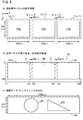
以下、図面を参照しつつ本発明の実施の形態について説明する。図1は、本発明の第1の実施の形態に係る表示装置1の斜視図である。表示装置1は、電子POP装置として利用可能な装置である。表示装置1は、液晶表示パネル11a,11b,11cと、筺体12と、取り付け部13と、チルト調節部14とを備える。
{First embodiment}
<Appearance and mounting state of
Hereinafter, embodiments of the present invention will be described with reference to the drawings. FIG. 1 is a perspective view of a
液晶表示パネル11a〜11cは、水平走査線方向に一列に並べられた汎用の小型液晶パネルであり、同様の構成を有している。液晶表示パネル11a〜11cは、一つの仮想パネルを構成し、全体として一つの画像を表示する。本実施の形態では、液晶表示パネル11a〜11cが、個別に画像を表示することはない。以下、液晶表示パネル11a〜11cをセットで説明するときには、液晶表示パネル11と呼ぶことにする。
The liquid
液晶表示パネル11a〜11cには外枠などの外縁部が存在するため、仮想パネルには画像を表示することができないギャップが発生する。仮想パネルに表示される映像は、ギャップの発生に伴って歪んで見えることがある。そこで、表示装置1は、ギャップ補正処理を実行することにより、仮想パネルに表示される映像の歪みを補正する。ギャップ補正処理の詳細については、後述する。
Since the liquid
筺体12は、液晶表示パネル11の制御部15(図6参照)などを収納するとともに、液晶表示パネル11a〜11cを同一平面上に固定する。取り付け部13は、表示装置1を固定する。チルト調節部14は、液晶表示パネル11の表示面の向きを調節する。
The
図2は、表示装置1の使用状態の一例を示す図である。表示装置1は、商品の陳列に用いられる陳列棚50の棚板51の前面に取り付けられる。棚板51の前面に取り付けられた表示装置1は、陳列棚50に陳列された商品の広告映像などを表示する。
FIG. 2 is a diagram illustrating an example of a usage state of the
表示装置1は、棚板51の前面などの限られたスペースに対応するために、複数の液晶表示パネル11a〜11cを組み合わせて仮想パネルを構成する。このため、表示装置1は、棚板51の前面のサイズに対応した液晶表示パネルを使用する必要がないため、大幅なコスト削減が可能となる。
The
図3(a)、図3(b)は、チルト調節部14の動作を説明する図である。表示装置1は、チルト調節部14を用いて液晶表示パネル11の表示面の向きを変更することができる。配線52は、表示装置1への電力供給などに用いられる。
FIG. 3A and FIG. 3B are diagrams for explaining the operation of the
表示面の向きは、ユーザが手動で変更することができる。なお、チルト調節部14は、ユーザが設定した角度に基づいて、表示面の向きを自動的に調節するようにしてもよい。
The orientation of the display surface can be changed manually by the user. Note that the
図3(a)は、表示面を水平方向に向けた状態を示す図である。たとえば、表示装置1が顧客の視線の高さとほぼ同じ高さの棚板51に取り付けられるときに、表示面の向きが水平方向となるように調節される。
FIG. 3A is a diagram showing a state in which the display surface is oriented in the horizontal direction. For example, when the
図3(b)は、表示面を上方に向けた状態を示す図である。表示装置1が陳列棚50の下側の棚板51に取り付けられたときなどに、表示面の向きが図3(b)のように上方に向けられる。なお、表示装置1が高所に取り付けられる場合には、表示面の向きを下向きに調節することができる。
FIG. 3B is a diagram illustrating a state where the display surface is directed upward. When the
液晶表示パネル11a〜11cの視野角は一般的に狭いとされている。しかし、表示装置1は、図3に示すように、表示面の向きを調節可能である。表示装置2は、取り付け位置に関係なく、陳列棚50の前にいる顧客に対して鮮明な映像を見せることできるため、販売促進の効果を高めることができる。
The viewing angles of the liquid
<仮想パネルの概要>
次に、液晶表示パネル11により構成される仮想パネルについて詳しく説明する。図4(a)は、液晶表示パネル11の表示領域を示す図である。
<Overview of virtual panel>
Next, a virtual panel constituted by the liquid
図4(a)に示すように、液晶表示パネル11a〜11cは、互いに隣接した状態で水平走査方向(X方向)に一列に配列されている。液晶表示パネル11a,11b,11cの表示領域110a,110b,110cのサイズは、X方向が320ピクセルであり、垂直走査方向(Y方向)が240ピクセルである。
As shown in FIG. 4A, the liquid
図4(b)は、仮想パネルの表示領域(以下、「仮想表示領域」という)20を示す図である。仮想表示領域20は、表示領域110a〜110cと、ギャップ21,21とにより構成される。ギャップ21は、表示領域110a,110bの間に挟まれた領域と、表示領域110b,110cの間に挟まれた領域である。ギャップ21は、液晶表示パネル11a〜11cの外枠などに対応しており、映像を表示することができない。ギャップ21のX方向の幅を、40ピクセルとする。仮想表示領域20のサイズは、X方向が1040ピクセルであり、Y方向が240ピクセルである。
FIG. 4B is a diagram showing a display area (hereinafter referred to as “virtual display area”) 20 of the virtual panel. The
図4(c)は、仮想表示領域20に表示される画像データ30を示す。画像データ30のサイズは、仮想表示領域20のサイズ(1040×240ピクセル)に対応している。画像データ30には、円301と直角三角形301が描画されている。表示装置1のユーザは、広告用の映像データである画像データ30を、予め記憶部151(図6参照)に格納しておく。
FIG. 4C shows the
<ギャップ補正処理の概要>
次に、ギャップ補正処理の概要を説明する。画像データ30は、仮想表示領域20に表示される場合、X方向に分割された状態で表示領域110a〜110cにそれぞれ表示される。しかし、画像データ30が単に分割された状態で表示領域110a〜110cに表示された場合、仮想表示領域20に表示される画像データ30に歪みが発生する。
<Overview of gap correction processing>
Next, an outline of the gap correction process will be described. When the
図5(a)は、画像データ30に描画された円301と直角三角形302とを、単に分割して表示領域110a,110bに表示した状態を示す図である。この場合、円301は、半円の状態で表示領域110a,110bに表示される。表示領域110a,110の間にはギャップ21が存在するため、仮想表示領域20に表示される円301は、楕円として顧客に認識される。同様に、単に分割されて表示領域110a,110bに表示された直角三角形302は、ギャップ21の存在により、のこぎり状の形状として顧客に認識される。
FIG. 5A is a diagram showing a state in which a
このように、画像データ30が単に分割されて表示領域110a〜110cに表示されることにより、表示装置1に表示される映像に対して、顧客が違和感を覚えるおそれがある。特に、画像データ30が動画像データである場合には、歪みが強調される。
As described above, the
そこで、表示装置1は、画像データ30を仮想表示領域20に表示する際に、ギャップ補正処理を実行する。ギャップ補正処理は、画像データ30のうちギャップ21に対応する領域のデータを、表示領域110a〜110cのいずれにも表示させない処理である。これにより、表示装置1は、顧客が違和感を覚えることの少ない映像を表示することが可能となる。
Therefore, the
図5(b)は、ギャップ補正処理の適用後に仮想表示領域20に表示された画像データ30を示す図である。図5(c)は、画像データ30においてギャップ21に対応する領域を示す図である。ギャップ補正処理により、画像データ30のうち、図5(c)に示すハッチングの領域が、表示領域110a〜110cのいずれにも表示されない。この結果、顧客は、視覚効果により、ギャップ21を挟んで表示領域110a,110bに表示されている円301が本来の形状(円)であると類推することができる。顧客は、ギャップ21を挟んで表示領域110b,110cに表示されている直角三角形302が、本来の形状(直角三角形)であると類推することができる。したがって、表示装置1は、仮想表示領域20に表示される画像データ30の歪みを抑制し、違和感の少ない映像を表示することができる。
FIG. 5B is a diagram illustrating the
<表示装置1の機能的構成>
図6は、表示装置1の機能的構成を示すブロック図である。表示装置1は、制御部15と、ブリッジ回路16とを備える。制御部15及びブリッジ回路16は、IC(Integrated Circuit)の状態で筺体12の中に設置される。
<Functional Configuration of
FIG. 6 is a block diagram illustrating a functional configuration of the
制御部15は、表示装置1の全体制御を行う。制御部15は、記憶部151と、デコーダ152と、フレームメモリ153と、仮想パネル制御部154とを備える。
The
記憶部151は、フラッシュメモリなどであり、画像データ30を格納する。画像データ30は、動画像データ及び静止画像データのいずれでもよい。制御部15は、記憶部151に代えて、メモリカードスロットを備えていてもよい。この場合、メモリカードスロットには、画像データ30が記録されたメモリカードが挿入される。
The
デコーダ152は、画像データ30をデコードして、仮想表示領域20に表示するフレームデータ60を作成する。フレームデータ60は、仮想表示領域20のアドレスに対応したピクセルデータ61の集合である。
The
フレームメモリ153は、デコーダ152が作成したフレームデータ60を格納する。
The
仮想パネル制御部154は、フレームメモリ153からフレームデータ60を読み出し、フレームデータ60に含まれるピクセルデータ61を、ブリッジ回路16に順次出力する。仮想パネル制御部154は、ピクセルデータ61の出力と同期して、仮想パネル制御信号62及びピクセルクロック63をブリッジ回路16に出力する。仮想パネル制御信号62は、仮想パネルの表示状態を制御する水平同期信号及び垂直同期信号などを含む。ピクセルクロック63は、ピクセルデータ61の入力と同期したクロック信号である。
The virtual
仮想パネル制御部154は、液晶表示パネル11a〜11cにより構成される単一の仮想パネルを制御し、液晶表示パネル11a〜11cを個別に制御することはない。仮想パネル制御部154は、仮想パネルに対応したサイズの液晶表示パネルを制御する機能を有していれば良い。このため、仮想パネル制御部154には、汎用の液晶表示パネルを制御するLCD(Liquid Crystal Display)コントローラを利用することができ、表示装置1の部品コストを削減することができる。
The virtual
ブリッジ回路16は、仮想パネル制御部154から出力されたピクセルデータ61の表示先を特定し、特定した表示先にピクセルデータ61を出力する。また、ブリッジ回路16は、ギャップ補正処理を実行する。
The
図7は、ブリッジ回路16の機能的構成を示すブロック図である。ブリッジ回路16は、ラインバッファ161a,161b,161cと、パラメータテーブル格納部162と、書き込み制御回路163と、液晶表示パネル制御回路164とを備える。
FIG. 7 is a block diagram showing a functional configuration of the
ラインバッファ161a〜161cは、液晶表示パネル11a〜11cにそれぞれ対応して設けられており、表示領域110a〜110cに対応するピクセルデータ61を格納する。ラインバッファ161a〜161cは、それぞれ第1メモリ165及び第2メモリ166を含む。第1メモリ165及び第2メモリ166は、FIFO(First In First Out)メモリである。第1メモリ165及び第2メモリ166の一方は、制御部15から出力されたピクセルデータ61の書き込み用として動作し、他方は、ラインバッファに書き込まれたピクセルデータ61を液晶表示パネル11に出力するために読み出し用として動作する。
The line buffers 161a to 161c are provided corresponding to the liquid
パラメータテーブル格納部162は、仮想表示領域20のアドレスと、表示領域110a〜110cとの対応関係を示すパラメータテーブル70を格納する。
The parameter
書き込み制御回路163は、入力されたピクセルデータ61の書き込み先となるラインバッファを、パラメータテーブル162に基づいて特定する。書き込み制御回路163は、特定したラインバッファに対して、入力されたピクセルデータ61の書き込みを指示する。
The
液晶表示パネル制御回路164は、ラインバッファ161a〜161cに書き込まれたピクセルデータ61を液晶表示パネル11に出力する。ピクセルデータ61は、各液晶表示パネル11を制御する液晶表示パネル制御信号64と同期して出力される。
The liquid crystal display
<ブリッジ回路16の動作>
図8は、ブリッジ回路16の動作を示すフローチャートである。図8において、第1液晶パネル〜第3液晶パネルは、液晶表示パネル11a〜11cにそれぞれ対応する。第1ラインバッファ〜第3ラインバッファは、ラインバッファ161a〜161cにそれぞれ対応する。
<Operation of
FIG. 8 is a flowchart showing the operation of the
ブリッジ回路16は、水平同期信号(H−Sync)が入力されることにより、図8に示す処理を開始する。ラインバッファ161a〜161cにおいて、第1メモリ165が書き込み用に設定されているとする。
The
書き込み制御回路163は、ピクセルデータ61が入力された場合(ステップS11でYes)、入力されたピクセルデータ61のXアドレスを確認する(ステップ12)。ピクセルデータ61のXアドレスは、仮想表示領域20に対応している。書き込み制御回路163は、水平同期信号が入力されてからピクセルクロック63をカウントしている。ピクセルクロック63のカウント値が、入力されたピクセルデータ61の仮想表示領域20におけるXアドレスとして用いられる。
When the
書き込み制御回路163は、入力されたピクセルデータ61のXアドレスが表示領域110aに対応するか否かを、パラメータテーブル70に基づいて判定する(ステップS13)。
The
図9は、パラメータテーブル70の一例を示す図である。パラメータテーブル70には、表示領域110a〜110cと、仮想表示領域20のXアドレスとの対応関係を示している。表示領域110aに対応する仮想パネルのXアドレスは、1〜320である。表示領域110aに対応する仮想パネルのXアドレスは、361〜680である。表示領域110cに対応する仮想パネルのXアドレスは、721〜1040である。仮想表示領域20のギャップ21に対応するXアドレス(321〜360,681〜720)は、パラメータテーブル70に設定されていない。
FIG. 9 is a diagram illustrating an example of the parameter table 70. The parameter table 70 shows the correspondence between the
入力されたピクセルデータ61のXアドレスが表示領域110aに対応する場合(ステップS13においてYes)、入力されたピクセルデータ61は、ラインバッファ161aの第1メモリ165に書き込まれる(ステップS14)。具体的には、ライトイネーブル信号65が、書き込み制御回路163からラインバッファ161aに入力される。ラインバッファ161aは、ライトイネーブル信号65の入力に応じて、入力されたピクセルデータ61を書き込む。このとき、ラインバッファ161b,161cがピクセルデータ61の書き込み処理を行うことはない。
If the X address of the
入力されたピクセルデータ61のXアドレスが表示領域110aに対応しない場合(ステップS13においてNo)、入力されたピクセルデータ61のXアドレスが表示領域110bに対応するか否かが判定される(ステップS15)。入力されたピクセルデータ61のXアドレスが表示領域110bに対応する場合(ステップS15でYes)、ラインバッファ161bの第1メモリ165に、入力されたピクセルデータ61が書き込まれる(ステップS16)。
If the X address of the
入力されたピクセルデータ61のXアドレスが表示領域110bに対応しない場合(ステップS15においてNo)、入力されたピクセルデータ61のXアドレスが表示領域110cに対応するか否かが判定される(ステップS17)。入力されたピクセルデータ61のXアドレスが表示領域110cに対応する場合(ステップS17でYes)、ラインバッファ161cの第1メモリ165に、入力されたピクセルデータ61が書き込まれる(ステップS18)。
When the X address of the
入力されたピクセルデータ61のXアドレスが表示領域110cに対応しない場合(ステップS17でNo)、書き込み制御回路163は、入力されたピクセルデータ61がギャップ21に対応すると判定し、入力されたピクセルデータ61を破棄する(ステップS19)。つまり、入力されたピクセルデータ61は、いずれの表示領域にも対応しないため、ラインバッファ161a〜161cのいずれにも書き込まれない。
When the X address of the
仮想表示領域20の一水平走査線分のピクセルデータ61の書き込みが終了していない場合(ステップS20においてNo)、ステップS11〜S20の処理が繰り返される。一方、仮想表示領域20の一水平走査線分のピクセルデータ61の書き込みが終了した場合(ステップS20においてYes)、各ラインバッファの第1メモリ165が書き込み用から読み出し用に切り替えられる(ステップS21)。同時に、各ラインバッファの第2メモリ166が書き込み用に切り替えられる。
When the writing of the
液晶表示パネル制御部164は、ラインバッファ161a〜161cにリードイネーブル信号66を出力する。これにより、ラインバッファ161a〜161cの第1メモリ165から、液晶表示パネル11a〜11cに対してピクセルデータ61がそれぞれ出力される(ステップS22)。第1メモリ165がFIFOメモリであるため、仮想表示領域20のXアドレスが小さいピクセルデータ61(第1メモリ165に最初に書き込まれたピクセルデータ61)から順次出力される。
The liquid crystal display
第1メモリ165からのピクセルデータ61の出力は、液晶表示パネル制御信号65と同期して行われる。液晶表示パネル制御信号65は、液晶表示パネル11a〜11cの水平同期信号、垂直同期信号及びピクセルクロックなどを含む。液晶表示パネル11a〜11cは、同一の構成であるため、液晶表示パネル制御部164は、液晶表示パネル11a〜11cで共通に利用できる単一の制御信号を生成すればよい。同一の構成を有する液晶表示パネル11a〜11cを利用することにより、液晶表示パネル11a〜11cの制御を簡略化することができる。ただし、本発明は、互いに構成の異なる液晶表示パネル11a〜11cの使用を制限するものではない。
The output of the
ラインバッファ161a〜161cから各液晶表示パネル11a〜11cへのピクセルデータ61の出力と並行して、ブリッジ回路16は、図7に示す処理を実行する。つまり、第1メモリ165からのピクセルデータ61の読み出しと並行して、次の水平走査線に対応するピクセルデータ61が、ラインバッファ161a〜161cの第2メモリ166に書き込まれる。このように、ラインバッファ161a〜161cをダブルバッファ構成とすることにより、ラインバッファの書き込み処理及び読み出し処理に伴って画像データ30の表示に遅延が発生することを抑制できる。
In parallel with the output of the
図8に示す処理では、ブリッジ回路16は、入力されたピクセルデータ61が液晶表示パネル11a〜11cに対応するか否かを連続的に判定しているが(ステップS13、S15、S17)、これに限られない。ブリッジ回路16は、ピクセルデータ61が仮想表示領域21のXアドレス順に入力されることを利用して、ピクセルデータ61が液晶表示パネル11a〜11cに対応するか否かを連続的に判定することのない処理を実行することも可能である。
In the process shown in FIG. 8, the
具体的には、ピクセルデータ61の入力が開始された場合、ブリッジ回路16は、パラメータテーブル70を参照してピクセルデータ61のXアドレスが1であることを確認する。ピクセルデータ61のXアドレスが320となるまで、ピクセルデータ61は、ラインバッファ161aに書き込まれる。ピクセルデータ61のXアドレスが321以上となった場合、ブリッジ回路16は、ギャップ21に対応するピクセルデータ61と判定して、ピクセルデータ61を破棄する。このとき、ブリッジ回路16は、ステップS13,S15,S17の処理を連続的に実行することはない。
Specifically, when the input of the
続いて、ピクセルデータ61のXアドレスが361となったときに、ラインバッファ161bへのピクセルデータ61の書き込みが開始される。ピクセルデータ61のXアドレスが680となるまで、ラインバッファ161bへの書き込み処理が継続される。ブリッジ回路16は、ピクセルデータ61が液晶表示パネル11aに対応するか否かを判定する(ステップS13)ことはない。ラインバッファ162cへのピクセルデータ61への書き込み処理も、同様に実行される。上記の処理は、ラインバッファ161a〜161cへのピクセルデータ61の書き込み処理をハードウェア回路によって実装する場合に有効である。上記の処理をハードウェア回路に適用することで、ラインバッファ161a〜161bへのピクセルデータ61への書き込み処理が効率化され、ハードウェア回路の規模を抑制することができる。
Subsequently, when the X address of the
以上説明したように、本実施の形態に係る表示装置1は、複数の液晶表示パネル11a〜11cを一列に配列して仮想パネルを構成し、仮想パネルに一つの画像データを表示する処理を行う。これにより、陳列棚50の幅に対応した液晶表示パネルを作成する必要がない。したがって、表示装置1の製造コストを大幅に削減することが可能となる。
As described above, the
また、制御部15は、複数の液晶表示パネル11a〜11cを単一の仮想パネルとして用いる。このため、表示装置1は、一つの画像データ30を分割して処理しなくてもよく、液晶表示パネル11a〜11cの制御を簡略化することができる。
In addition, the
また、表示装置1にチルト調節部14を設けることにより、液晶表示パネル11の表示面の向きを調節することができる。したがって、液晶表示パネル11の表示面の向きを顧客が映像を見やすい向きに調節することにより、販売促進効果を高めることが可能となる。
Further, by providing the
なお、本実施の形態では、表示装置1が3つの液晶表示パネル11a〜11cを有する例について説明したが、これに限られない。陳列棚50の幅に応じて、表示装置1が有する液晶表示パネルを2つにしてもよいし、3つ以上としてもよい。
In the present embodiment, the example in which the
また、本実施の形態では、ピクセルデータ61がピクセルクロック63と同期してブリッジ回路16に入力される例について説明したが、これに限られない。たとえば、ピクセルデータ61は、仮想表示領域20におけるアドレス情報とともにブリッジ回路16に入力されてもよい。この場合、ブリッジ回路16は、アドレス情報に基づいて、ピクセルデータ61がどの表示領域に対応するかを判定する。
In this embodiment, the example in which the
また、本実施の形態では、液晶表パネル11a〜11cとして、水平走査線方向の長さが垂直走査線方向の長さよりも大きいものを使用する例について説明したが、これに限られない。液晶表示パネル11a〜11cとして、垂直走査線方向の長さが水平走査線方向の長さよりも大きいものを使用してもよい。図4(a)に示す仮想表示領域21を形成するためには、液晶表示パネル11a〜11cを90度回転させて、垂直走査線方向に一列に配列させる必要がある。この結果、仮想表示領域21のXアドレスとYアドレスとが入れ替わることになる。
In the present embodiment, the liquid
したがって、上記第1の実施の形態とは、以下の点で処理が異なる。デコーダ152は、動画像データ35から生成したフレームデータ60を90度回転させた上で、フレームメモリ153に書き込む。ギャップ補正処理が垂直走査線方向を基準として行われるため、パラメータテーブル70には、表示領域110a〜110cと、仮想表示領域21のYアドレスとの対応情報が記録される。ブリッジ回路16には一水平走査線単位でピクセルデータ61が入力される点では同じであるが、ピクセルデータ61をXアドレスに応じてラインバッファ161a〜161cに分割する必要がない。このため、ブリッジ回路16は、ラインバッファ161aのみを有していればよい。
Therefore, the processing differs from the first embodiment in the following points. The
{第2の実施の形態}
以下、本発明の第2の実施の形態について説明する。本実施の形態では、複数の表示装置によって仮想パネルが構成される。以下、上記第1の実施の形態と異なる点を中心に説明し、同様の点については説明を省略する。
{Second Embodiment}
Hereinafter, a second embodiment of the present invention will be described. In this embodiment, a virtual panel is configured by a plurality of display devices. The following description will focus on the differences from the first embodiment, and the description of the same points will be omitted.
図10は、本実施の形態に係る表示装置1,8の構成と配置状態とを示す図である。表示装置1,8の構成は、上記第1の実施の形態に係る表示装置1の構成と基本的に同じである。制御部15では、記憶部151及びデコーダ152以外の表示を省略している。
FIG. 10 is a diagram showing a configuration and an arrangement state of the
記憶部151は、画像データ30に代えて、画像データ35を格納する。画像データ35は、表示装置1,8により構成される仮想パネルの表示領域に対応したサイズで作成されている。デコーダ152は、画像データ35のデコード範囲を指定するデコード範囲指定情報36を保持している。
The
表示装置1は、液晶表示パネル11a〜11cを備える。表示装置8は、液晶表示パネル81a〜81cを備える。液晶表示パネル11a〜11c,81a〜81cがX方向(水平走査方向)に一列に並ぶように、表示装置1,8は配置される。
The
図11(a)は、表示装置1,8により構成される仮想パネルの表示領域(以下、「仮想表示領域」という)25を示す図である。仮想表示領域25は、表示領域110a〜110c,810a〜810cと、ギャップ21,21,21,21と、装置間ギャップ26とにより構成される。
FIG. 11A is a diagram showing a display area (hereinafter referred to as “virtual display area”) 25 of a virtual panel constituted by the
仮想表示領域25のサイズは、X方向が2140ピクセル、Y方向が240ピクセルである。表示装置1は、仮想表示領域25のうちXアドレスが1〜1040ピクセルの領域に対応する。表示装置8は、仮想表示領域25のうちX方向で1101〜2140ピクセルの領域に対応する。仮想表示領域25には、表示領域110a〜110c,810a〜801cの間に発生するギャップ21の他に、表示装置1,8により形成される装置間ギャップ26が発生する。装置間ギャップ26は、X方向の幅を60ピクセルであり、Xアドレスが1041〜1100の領域に対応する。
The size of the
図11(b)は、仮想表示領域25に表示される画像データ35を示す図である。画像データ35は、仮想表示領域25のサイズに対応して作成されるため、X方向のサイズが2140ピクセル、Y方向のサイズが240ピクセルとなる。
FIG. 11B is a diagram showing the
仮想表示領域25に画像データ35を表示させる場合、表示装置1、8は、画像データ35をデコードして、デコード範囲指定情報36で指定された範囲に対応するフレームデータ60を作成する。表示装置1では、デコード範囲指定情報36として、X方向のアドレス1〜1140が設定されている。表示装置8では、デコード範囲指定情報36として、X方向のアドレス1101〜2140が設定されている。この結果、画像データ35は、図11(c)に示すような状態で表示される。
When displaying the
ギャップ21に対応する領域は、上記第1の実施の形態で説明したように、液晶表示パネル11a〜11c,81a〜81cのいずれにも表示されない。
The region corresponding to the
また、装置間ギャップ26に対応する領域(Xアドレスが1041〜1100の範囲)は、表示装置1,8のいずれにも表示されない。これは、表示装置1,8のデコード範囲指定情報36のいずれにも、装置間ギャップ26に対応するXアドレスが指定されていないためである。この結果、図10(c)に示すように、装置間ギャップ26の位置に表示される直角三角形212が、のこぎり状の形状ではなく、本来の形状(直角三角形)として類推できるように表示される。
Further, the region corresponding to the inter-device gap 26 (X address range of 1041 to 1100) is not displayed on any of the
このように、表示装置1,8は、画像データ35のうち、それぞれのデコード範囲指定情報36で指定された範囲をデコードしてピクセルデータ61を生成し、ピクセルデータ61をそれぞれの仮想パネルに表示する。デコード範囲指定情報36は、装置間ギャップ26を考慮して設定される。したがって、仮想表示領域25に画像データ35が表示される際に、装置間ギャップ26により発生する画像データ35の歪みを補正することができる。
In this way, the
なお、上記第2の実施の形態では、二つの表示装置1,8を用いる例について説明したが、図2に示すように、棚板51の前面に並べられた3つ以上の表示装置を用いて仮想パネルを構成してもよい。表示装置1,1・・・のデコード部152が保持するデコード範囲指定情報36に、各表示装置に対応する仮想表示領域のアドレス範囲を設定すればよい。
In the second embodiment, the example using two
また、上記第2の実施の形態では、二つの表示装置1,8のデコーダ152は、デコード範囲指定情報36に基づいて画像データ35をデコードする例について説明したが、これに限られない。表示装置1,8は、仮想表示領域25のうちそれぞれの表示領域に対応する画像データ35を保持してもよい。表示装置1は、Xアドレスが1〜1040の領域に対応する画像データ35を保持する。表示装置8は、Xアドレスが1101〜2140の領域に対応する画像データを保持する。この場合、表示装置1,8は、上記第1の実施の形態と同様の処理を実行する。画像データ35のデータサイズを抑制することができるため、記憶部151に大容量のフラッシュメモリを用いる必要がない。したがって、表示装置1,8のコストを削減できる。
In the second embodiment, the
また、上記第2の実施の形態では、水平走査方向に配列された複数の表示装置を用いて単一の画像データ35を表示する例について説明したが、これに限られない。たとえば、垂直走査方向に配列された複数の表示装置を用いて、一つの画像データを表示してもよい。たとえば、図2に示す棚板51,51に設置された6つの表示装置1を用いて、一つの画像データを表示することができる。Y方向のデコード範囲を指定するために、各表示装置1のデコード範囲指定情報36には、Y方向のアドレス範囲が指定される。
In the second embodiment, the example in which the
このとき、Y方向の装置間ギャップを考慮して、各表示装置1のデコード領域範囲情報36にY方向のアドレス範囲を設定してもよい。これにより、Y方向の装置間ギャップに伴う画像の歪みを抑制できる。
At this time, an address range in the Y direction may be set in the decode area range information 36 of each
Y方向に生じるギャップの大きさは、棚板51,51の間隔にほぼ対応する。このため、Y方向の装置間ギャップを補正しても、視覚効果によりY方向の映像の歪みを抑制する効果が十分に得られないケースがある。この場合、Y方向のアドレス範囲を設定する際に、Y方向の装置間ギャップを考慮しなくてもよい。Y方向の装置間ギャップを考慮しない場合、Y方向の装置間ギャップを考慮する場合と比べて、画像データ35のデータサイズを抑制することができる。
The size of the gap generated in the Y direction substantially corresponds to the interval between the
1,8 表示装置
11,11a,11b,11c 液晶表示パネル
12 筐体
13 取り付け部
14 チルト調節部
15 制御部
16 ブリッジ回路
151 記憶部
152 デコーダ
153 フレームメモリ
154 仮想パネル制御部
161a,161b,161c ラインバッファ
162 パラメータテーブル格納部
163 書き込み制御回路
164 液晶表示パネル制御回路
DESCRIPTION OF
Claims (9)
画像データをデコードし、前記複数の表示パネルにより構成される仮想表示領域に対応する画素情報を生成し、前記仮想表示領域に対応する画素情報を、前記仮想表示領域に前記画素情報を表示させると仮想した場合に必要とされる水平同期信号及びピクセルクロックに同期させて出力する画素情報生成部と、
前記仮想表示領域と、各表示パネルの個別表示領域との対応関係を示す対応情報を格納する対応情報格納部と、
前記画素情報生成部から出力される前記仮想表示領域の前記水平同期信号及び前記ピクセルクロックに基づいて、前記仮想表示領域の一水平走査線に含まれる画素情報のうち各表示パネルに対応する画素情報を前記対応情報に基づいて特定し、前記一水平走査線に含まれる画素情報の特定を終了するたびに各表示パネルに対応する画素情報を各表示パネルの制御情報とともに各表示パネルに出力する表示パネル特定部と、
を備えることを特徴とする表示装置。 A plurality of display panels arranged in a horizontal scanning line direction ;
Decoding image data, generating pixel information corresponding to a virtual display area constituted by the plurality of display panels, displaying pixel information corresponding to the virtual display area, and displaying the pixel information in the virtual display area A pixel information generation unit that outputs in synchronization with a horizontal synchronization signal and a pixel clock required in a virtual case ;
A correspondence information storage unit that stores correspondence information indicating a correspondence relationship between the virtual display area and the individual display area of each display panel;
Pixel information corresponding to each display panel among pixel information included in one horizontal scanning line of the virtual display area based on the horizontal synchronization signal and the pixel clock of the virtual display area output from the pixel information generation unit Is displayed based on the correspondence information, and the pixel information corresponding to each display panel is output to each display panel together with the control information of each display panel every time the specification of the pixel information included in the one horizontal scanning line is finished. A panel specific part,
A display device comprising:
前記複数の表示パネルは、
相互に隣接する第1の表示パネル及び第2の表示パネル、
を含み、
前記表示パネル特定部は、
前記一水平走査線に含まれる画素情報のうち前記第1の表示パネルの個別表示領域と前記第2の表示パネルの個別表示領域との間に挟まれたギャップ領域に対応する画素情報を、前記対応情報に基づいて判定する判定部と、
前記ギャップ領域に対応する画素情報を破棄する画素情報破棄部と、
を含むことを特徴とする表示装置。 The display device according to claim 1,
The plurality of display panels are
A first display panel and a second display panel adjacent to each other;
Including
The display panel specifying unit includes:
Pixel information corresponding to a gap region sandwiched between the individual display region of the first display panel and the individual display region of the second display panel among the pixel information included in the one horizontal scanning line, A determination unit for determining based on correspondence information;
A pixel information discarding unit for discarding pixel information corresponding to the gap region;
A display device comprising:
前記判定部は、
前記一水平走査線に含まれる画素情報のうち各表示パネルの個別表示領域のいずれにも対応しない画素情報を、前記ギャップ領域に対応する画素情報であると判定することを特徴とする表示装置。 The display device according to claim 2,
The determination unit
A display device, wherein pixel information that does not correspond to any of the individual display areas of each display panel among the pixel information included in the one horizontal scanning line is determined to be pixel information corresponding to the gap area.
前記画素情報生成部は、
前記画像データのうちデコードする範囲を指定するデコード範囲指定部、
を含み、
前記画素情報生成部は、前記画像データのうち前記デコード範囲指定部により指定された範囲をデコードして画素情報を生成することを特徴とする表示装置。 The display device according to any one of claims 1 to 3,
The pixel information generation unit
A decoding range designating unit for designating a decoding range in the image data;
Including
The display device, wherein the pixel information generation unit generates pixel information by decoding a range designated by the decode range designation unit in the image data.
前記第1の表示パネル及び前記第2の表示パネルが隣接する方向は、各表示パネルの水平走査線方向であることを特徴とする表示装置。 The display device according to claim 2,
A display device, wherein a direction in which the first display panel and the second display panel are adjacent is a horizontal scanning line direction of each display panel.
前記表示パネル特定部は、
各表示パネルに対応する複数のバッファと、
各表示パネルに対応する画素情報を各表示パネルに対応するバッファに格納するバッファ書き込み部と、
前記一水平走査線に含まれる画素情報の表示先が特定された場合、各バッファに書き込まれた画素情報を各表示パネルに出力する出力制御部と、
を含むことを特徴とする表示装置。 The display device according to claim 5,
The display panel specifying unit includes:
Multiple buffers corresponding to each display panel;
A buffer writing unit for storing pixel information corresponding to each display panel in a buffer corresponding to each display panel;
If the display destination of the pixel information contained in the prior SL one horizontal scanning line is specified, and an output controller for outputting the pixel information written in each buffer in each display panel,
A display device comprising:
各表示パネルの水平走査線の数及び一水平走査線あたりの画素数は同一であり、
各表示パネルに出力される制御情報は、同一の情報であることを特徴とする表示装置。 The display device according to claim 6,
The number of horizontal scanning lines and the number of pixels per horizontal scanning line of each display panel are the same,
A display device characterized in that the control information output to each display panel is the same information.
前記複数の表示パネルの表示面の角度を調節するチルト調節部、
を備えることを特徴とする表示装置。 The display device according to any one of claims 1 to 7, further comprising:
A tilt adjusting unit for adjusting an angle of a display surface of the plurality of display panels;
A display device comprising:
各表示パネルは、液晶表示パネルであることを特徴とする表示装置。 The display device according to any one of claims 1 to 8,
Each display panel is a liquid crystal display panel.
Priority Applications (5)
| Application Number | Priority Date | Filing Date | Title |
|---|---|---|---|
| JP2009172796A JP5611552B2 (en) | 2009-07-24 | 2009-07-24 | Display device |
| CN201080032998.3A CN102473393B (en) | 2009-07-24 | 2010-06-15 | Display device |
| EP10802138A EP2458580A4 (en) | 2009-07-24 | 2010-06-15 | Display apparatus |
| PCT/JP2010/060130 WO2011010517A1 (en) | 2009-07-24 | 2010-06-15 | Display apparatus |
| US13/386,449 US9343001B2 (en) | 2009-07-24 | 2010-06-15 | Display device using a display panel which prevents image distortion |
Applications Claiming Priority (1)
| Application Number | Priority Date | Filing Date | Title |
|---|---|---|---|
| JP2009172796A JP5611552B2 (en) | 2009-07-24 | 2009-07-24 | Display device |
Publications (2)
| Publication Number | Publication Date |
|---|---|
| JP2011027950A JP2011027950A (en) | 2011-02-10 |
| JP5611552B2 true JP5611552B2 (en) | 2014-10-22 |
Family
ID=43498993
Family Applications (1)
| Application Number | Title | Priority Date | Filing Date |
|---|---|---|---|
| JP2009172796A Expired - Fee Related JP5611552B2 (en) | 2009-07-24 | 2009-07-24 | Display device |
Country Status (5)
| Country | Link |
|---|---|
| US (1) | US9343001B2 (en) |
| EP (1) | EP2458580A4 (en) |
| JP (1) | JP5611552B2 (en) |
| CN (1) | CN102473393B (en) |
| WO (1) | WO2011010517A1 (en) |
Families Citing this family (13)
| Publication number | Priority date | Publication date | Assignee | Title |
|---|---|---|---|---|
| KR101415571B1 (en) * | 2007-10-15 | 2014-07-07 | 삼성디스플레이 주식회사 | Display device and driving method of the same |
| WO2013089705A1 (en) * | 2011-12-14 | 2013-06-20 | Intel Corporation | Micro digital signage hardware integration |
| KR102028336B1 (en) * | 2012-12-03 | 2019-10-04 | 삼성전자주식회사 | Display apparatus for displaying multi screen and method for controlling thereof |
| US20150279037A1 (en) * | 2014-01-11 | 2015-10-01 | Userful Corporation | System and Method of Video Wall Setup and Adjustment Using Automated Image Analysis |
| JP6347647B2 (en) * | 2014-04-04 | 2018-06-27 | 株式会社平和 | Game machine |
| US10901548B2 (en) * | 2015-04-07 | 2021-01-26 | Omnivision Technologies, Inc. | Touch screen rear projection display |
| JP6618739B2 (en) * | 2015-09-08 | 2019-12-11 | シャープ株式会社 | Multi-screen display system and display control program |
| US10152291B2 (en) * | 2015-10-16 | 2018-12-11 | Omnivision Technologies, Inc. | Multi-projector display box for use in retail marketing |
| US10354569B2 (en) * | 2017-02-08 | 2019-07-16 | Microsoft Technology Licensing, Llc | Multi-display system |
| AU2017438991B2 (en) * | 2017-11-10 | 2023-07-27 | Vusiongroup Gmbh | Electronic shelf label system with sectional control of display content |
| CN113050902A (en) * | 2021-03-31 | 2021-06-29 | 京东方科技集团股份有限公司 | Spliced screen and control method and system thereof |
| US12022964B1 (en) | 2023-01-31 | 2024-07-02 | Carter-Hoffmann LLC | Heated display cabinet |
| US12446711B2 (en) | 2023-01-31 | 2025-10-21 | Carter-Hoffmann LLC | Heated display cabinet |
Family Cites Families (17)
| Publication number | Priority date | Publication date | Assignee | Title |
|---|---|---|---|---|
| WO1991007739A1 (en) * | 1989-11-14 | 1991-05-30 | Imtech International, Inc. | Moving message display method and apparatus |
| JPH08211849A (en) * | 1995-02-02 | 1996-08-20 | Casio Comput Co Ltd | Display controller |
| US6104414A (en) * | 1997-03-12 | 2000-08-15 | Cybex Computer Products Corporation | Video distribution hub |
| JP3595153B2 (en) * | 1998-03-03 | 2004-12-02 | 株式会社 日立ディスプレイズ | Liquid crystal display device and video signal line driving means |
| JP2001100683A (en) | 1999-09-27 | 2001-04-13 | Mitsubishi Electric Engineering Co Ltd | Image electronic pop device |
| JP2003066933A (en) * | 2001-08-23 | 2003-03-05 | Nec Corp | Method and device for display |
| JP2003180494A (en) * | 2001-12-14 | 2003-07-02 | Tanahashi Kogyo Kk | Display for shelf board |
| US6816177B2 (en) * | 2002-01-28 | 2004-11-09 | Tony Wang | Display observation angle of which is multidirectionally adjustable |
| JP2003224788A (en) * | 2002-01-31 | 2003-08-08 | Ricoh Co Ltd | High definition image display apparatus and method |
| JP2003330382A (en) * | 2002-05-10 | 2003-11-19 | Funai Electric Co Ltd | Electronic pop and fixture of monitor |
| JP2005227579A (en) * | 2004-02-13 | 2005-08-25 | Seiko Epson Corp | Information display device and information display program |
| JP4639972B2 (en) | 2005-06-07 | 2011-02-23 | 日本ビクター株式会社 | Image display device and image display method |
| JP4913514B2 (en) | 2006-03-28 | 2012-04-11 | 東芝テック株式会社 | Display shelf and display shelf system |
| JP2008289786A (en) * | 2007-05-28 | 2008-12-04 | Seiko Epson Corp | Image display device, game machine, image display method, image display program, and recording medium |
| US8013804B2 (en) * | 2007-05-30 | 2011-09-06 | Lenovo (Singapore) Pte. Ltd, | System and method for graphics remapping in hypervisor |
| KR101415571B1 (en) * | 2007-10-15 | 2014-07-07 | 삼성디스플레이 주식회사 | Display device and driving method of the same |
| US8537166B1 (en) * | 2007-12-06 | 2013-09-17 | Nvidia Corporation | System and method for rendering and displaying high-resolution images |
-
2009
- 2009-07-24 JP JP2009172796A patent/JP5611552B2/en not_active Expired - Fee Related
-
2010
- 2010-06-15 CN CN201080032998.3A patent/CN102473393B/en not_active Expired - Fee Related
- 2010-06-15 WO PCT/JP2010/060130 patent/WO2011010517A1/en not_active Ceased
- 2010-06-15 EP EP10802138A patent/EP2458580A4/en not_active Withdrawn
- 2010-06-15 US US13/386,449 patent/US9343001B2/en not_active Expired - Fee Related
Also Published As
| Publication number | Publication date |
|---|---|
| EP2458580A4 (en) | 2012-12-26 |
| US20120119977A1 (en) | 2012-05-17 |
| CN102473393B (en) | 2015-08-26 |
| CN102473393A (en) | 2012-05-23 |
| US9343001B2 (en) | 2016-05-17 |
| JP2011027950A (en) | 2011-02-10 |
| WO2011010517A1 (en) | 2011-01-27 |
| EP2458580A1 (en) | 2012-05-30 |
Similar Documents
| Publication | Publication Date | Title |
|---|---|---|
| JP5611552B2 (en) | Display device | |
| CN102981794B (en) | A kind of splicing display method of PowerPoint | |
| CN108885851B (en) | Electronic display stabilization at graphics processing unit | |
| US6986583B2 (en) | Table type display device and an assembling method thereof | |
| JP2006246496A5 (en) | ||
| JPWO2009147795A1 (en) | Video processing system | |
| JP2009145875A5 (en) | ||
| CN114125328A (en) | Multi-source input multi-screen splicing system and method and display device | |
| CN103399720B (en) | A kind of data processing method and a kind of electronic equipment | |
| US20060125835A1 (en) | DMA latency compensation with scaling line buffer | |
| JP2015138084A (en) | Video display device and video display system | |
| US20150145892A1 (en) | Display apparatus for configuring a video wall, display system, and control method thereof | |
| JP2004007315A (en) | Head mounted display | |
| US7817166B2 (en) | Stereo windowing system with translucent window support | |
| CN114982250B (en) | Signal processing method and device, display device | |
| JP2004252345A (en) | Presentation apparatus | |
| EP1331815A3 (en) | Projection-type display device having distortion correcting function | |
| JP4746912B2 (en) | Image signal processing circuit and image display device | |
| JPH09116827A (en) | Reduction video signal processing circuit | |
| JP5958224B2 (en) | Display device and display method | |
| US8482603B2 (en) | Device and method for 3-D display control | |
| JP5732887B2 (en) | Frame memory controller | |
| JP2011211274A (en) | Image display apparatus, projector, and data acquiring method in the image display apparatus | |
| JP2011113381A (en) | Image display method and device of the same, method for generating image data for scroll display, and recording medium | |
| JP7485821B1 (en) | Image processing device and image processing method |
Legal Events
| Date | Code | Title | Description |
|---|---|---|---|
| A621 | Written request for application examination |
Free format text: JAPANESE INTERMEDIATE CODE: A621 Effective date: 20120229 |
|
| A131 | Notification of reasons for refusal |
Free format text: JAPANESE INTERMEDIATE CODE: A131 Effective date: 20130730 |
|
| A521 | Request for written amendment filed |
Free format text: JAPANESE INTERMEDIATE CODE: A523 Effective date: 20130925 |
|
| A131 | Notification of reasons for refusal |
Free format text: JAPANESE INTERMEDIATE CODE: A131 Effective date: 20131126 |
|
| A521 | Request for written amendment filed |
Free format text: JAPANESE INTERMEDIATE CODE: A523 Effective date: 20140124 |
|
| A02 | Decision of refusal |
Free format text: JAPANESE INTERMEDIATE CODE: A02 Effective date: 20140318 |
|
| A521 | Request for written amendment filed |
Free format text: JAPANESE INTERMEDIATE CODE: A523 Effective date: 20140616 |
|
| A911 | Transfer to examiner for re-examination before appeal (zenchi) |
Free format text: JAPANESE INTERMEDIATE CODE: A911 Effective date: 20140624 |
|
| TRDD | Decision of grant or rejection written | ||
| A01 | Written decision to grant a patent or to grant a registration (utility model) |
Free format text: JAPANESE INTERMEDIATE CODE: A01 Effective date: 20140902 |
|
| A61 | First payment of annual fees (during grant procedure) |
Free format text: JAPANESE INTERMEDIATE CODE: A61 Effective date: 20140903 |
|
| R150 | Certificate of patent or registration of utility model |
Ref document number: 5611552 Country of ref document: JP Free format text: JAPANESE INTERMEDIATE CODE: R150 |
|
| R250 | Receipt of annual fees |
Free format text: JAPANESE INTERMEDIATE CODE: R250 |
|
| R250 | Receipt of annual fees |
Free format text: JAPANESE INTERMEDIATE CODE: R250 |
|
| R250 | Receipt of annual fees |
Free format text: JAPANESE INTERMEDIATE CODE: R250 |
|
| LAPS | Cancellation because of no payment of annual fees |