JP4746912B2 - Image signal processing circuit and image display device - Google Patents
Image signal processing circuit and image display device Download PDFInfo
- Publication number
- JP4746912B2 JP4746912B2 JP2005131186A JP2005131186A JP4746912B2 JP 4746912 B2 JP4746912 B2 JP 4746912B2 JP 2005131186 A JP2005131186 A JP 2005131186A JP 2005131186 A JP2005131186 A JP 2005131186A JP 4746912 B2 JP4746912 B2 JP 4746912B2
- Authority
- JP
- Japan
- Prior art keywords
- image
- memory unit
- output
- order
- input
- Prior art date
- Legal status (The legal status is an assumption and is not a legal conclusion. Google has not performed a legal analysis and makes no representation as to the accuracy of the status listed.)
- Expired - Fee Related
Links
Images


Landscapes
- Studio Circuits (AREA)
- Control Of Indicators Other Than Cathode Ray Tubes (AREA)
- Controls And Circuits For Display Device (AREA)
- Control Of El Displays (AREA)
- Control Of Gas Discharge Display Tubes (AREA)
- Image Input (AREA)
- Liquid Crystal Display Device Control (AREA)
Description
この発明は、画像信号処理回路および画像表示装置に関し、特に、コンピュータから出力される画像データやテレビジョン信号を、画像表示装置に表示するための画像信号処理回路に適用して好適なものである。 The present invention relates to an image signal processing circuit and an image display device, and is particularly suitable for application to an image signal processing circuit for displaying image data and television signals output from a computer on an image display device. .
従来、画像表示装置に表示する画像としては、コンピュータ画像、デジタルカメラの画像、およびテレビジョン信号の画像などの様々な種類が存在する。そして、これらの画像のフォーマットに関しても多数存在する。 Conventionally, there are various types of images displayed on the image display device, such as computer images, digital camera images, and television signal images. Many of these image formats exist.
これらの画像フォーマットが固定された画像表示装置である場合には、画像フォーマットに合わせた画像表示装置を選択することにより、この画像フォーマットに対応させることができる。ところが、汎用の画像表示装置においては、画像表示装置に画像を表示させるためには、その画像に対しても画像処理を施す必要がある。 In the case of an image display device in which these image formats are fixed, it is possible to correspond to this image format by selecting an image display device that matches the image format. However, in a general-purpose image display device, in order to display an image on the image display device, it is necessary to perform image processing on the image.
この画像表示装置における画像処理として、代表的には、IP変換や、フレームレート変換、または解像度変換などがある。これらのうちのIP変換とは、テレビジョン信号のNTSC信号のようなインターレース信号をプログレッシブ信号に変換するものである。また、フレームレート変換とは、画面の切り換えレートの変換である。また、解像度変換とは、横方向の画素数および縦方向の走査線数を変換するものである。 The image processing in this image display device typically includes IP conversion, frame rate conversion, or resolution conversion. Of these, IP conversion is to convert an interlace signal such as an NTSC signal of a television signal into a progressive signal. The frame rate conversion is conversion of the screen switching rate. The resolution conversion is to convert the number of pixels in the horizontal direction and the number of scanning lines in the vertical direction.
これらの画像処理を実行する場合において、フレームメモリを用いる構成が知られている。このフレームメモリは、1画面分の画像データを格納しておき、画像処理の必要に応じてデータを読み出して処理を行うものである。そして、このフレームメモリを採用することにより、上述した画像処理のみならず、特殊画像処理を実行することも可能となる。 In the case of executing these image processes, a configuration using a frame memory is known. This frame memory stores image data for one screen, and reads and processes data as needed for image processing. By adopting this frame memory, not only the above-described image processing but also special image processing can be executed.
また、特許文献1には、フレームメモリへの書き込み順序または読み出し順序を制御することによって、画像の反転および回転と拡大および縮小とを行う技術が開示されている。 Japanese Patent Application Laid-Open No. 2004-228561 discloses a technique for performing inversion, rotation, enlargement, and reduction of an image by controlling the order of writing to or reading from a frame memory.
また、近年、1つの画像表示装置に複数の画面を表示するマルチ画面表示が一般に行われてきている。そして、特許文献1および特許文献2には、このようなマルチ画面表示に関して、複数のメモリ空間を使用することによりマルチ画面表示を行う手法が開示されている。
In recent years, multi-screen display in which a plurality of screens are displayed on one image display device has been generally performed.
また、特許文献3においては、SDRAM(Synchronous DRAM)のバーストモードを使用して画像の反転、回転などの処理を行う手法が開示されている。この手法においては、画像データを縦横が所定の画素数で構成されたブロックに分割し、ブロック毎にバースト転送を行い、そのブロック内でデータの順番を入れ替えることによってブロック内データの反転、回転などの処理を行い、該当するブロックの書き込み、または読み出し順序を入れ替えることによって画像全体の反転や回転などの処理を実現する。 Japanese Patent Application Laid-Open No. 2004-228688 discloses a technique for performing processing such as image inversion and rotation using a burst mode of SDRAM (Synchronous DRAM). In this method, image data is divided into blocks each having a predetermined number of pixels in the vertical and horizontal directions, burst transfer is performed for each block, and the order of the data is changed within the block, so that the data in the block is inverted, rotated, etc. This process is performed, and the process of inversion and rotation of the entire image is realized by changing the writing or reading order of the corresponding block.
ところで、SDRAMなどのフレームメモリを用いてリアルタイム処理を行う場合には、SDRAMのバーストモードを使用するのが好ましい。そして、図11に示すように、このバーストモードにおいては、パイプライン処理を利用して連続してデータ転送を行うことが可能となる。ただし、バーストモードにおけるアドレスカウントは、シーケンシャルまたはインタリーブによるカウントアップとなる。 By the way, when performing real-time processing using a frame memory such as SDRAM, it is preferable to use the burst mode of SDRAM. As shown in FIG. 11, in this burst mode, data transfer can be continuously performed using pipeline processing. However, the address count in the burst mode is incremented by sequential or interleave.
したがって、特許文献1および特許文献2に記載された技術に対しては、バーストモードを使用することが極めて困難である。具体的には、特許文献1および特許文献2に記載された方法においては、メモリへの1アクセスごとに、ロウアドレスおよびカラムアドレスを指定しなければならない。さらに、動画処理においては、メモリアクセスの処理速度を向上させる必要がある。
したがって、この発明の目的は、比較的簡易な回路構成で反転表示を実行可能な画像処理装置およびこの画像処理装置を備えた画像表示装置を提供することにある。 Accordingly, an object of the present invention is to provide an image processing apparatus capable of executing reverse display with a relatively simple circuit configuration and an image display apparatus provided with the image processing apparatus.
上記目的を達成するために、この発明の第1の発明は、
順次入力される画像信号をライン単位に格納する第1のメモリ部と、
第1のメモリ部から出力される画像信号を複数ライン分格納することが可能な第2のメモリ部と、
第1のメモリ部および第2のメモリ部を制御する制御回路と、を有することを特徴とする画像処理装置である。
制御回路は、第1のメモリ部にライン単位に格納された画像信号のうち、第1のメモリ部の先頭アドレスから任意に設定された列反転位置に対応するアドレスまでの画像信号を第1のメモリ部に入力された第1の順序で第2のメモリ部に出力した後、列反転位置に対応するアドレスから先頭アドレスまでの画像信号を第1のメモリ部に入力された順序とは逆の第2の順序で出力し、当該出力された画像信号を第2のメモリ部に順次入力して複数のライン分の画像信号が格納されるように制御するとともに、第2のメモリ部に複数ライン分格納された画像信号のうち、第1の順序で第1のメモリ部から出力された画像信号は第2のメモリ部に入力されたライン順で出力するとともに、第2の順序で第1のメモリ部から出力された画像信号は第2のメモリ部に格納されたライン順とは逆の順序で出力する制御を行うことが好ましい。
又は、制御回路は、第1のメモリ部にライン単位に格納された画像信号を出力する際、格納された画像信号のうち、第1のメモリ部の先頭アドレスから任意に設定された列反転位置に対応するアドレスまでの画像信号を第1のメモリ部に入力された第1の順序で第2のメモリ部に出力した後、列反転位置に対応するアドレスから先頭アドレスまでの画像信号を第1のメモリ部に入力された順序とは逆の第2の順序で第2のメモリ部に出力するように制御し、当該出力された画像信号を第2のメモリ部にライン単位に複数ライン分格納する際に、第1の順序で第1のメモリ部から出力された画像信号は第2のメモリ部に入力されたライン順で格納するとともに、第2の順序で第1のメモリ部から出力された画像信号は第2のメモリに入力されたライン順とは逆の順序で格納する制御を行うことが好ましい。
In order to achieve the above object, the first invention of the present invention provides:
A first memory unit for storing sequentially input image signals in units of lines;
A second memory unit capable of storing a plurality of lines of image signals output from the first memory unit;
An image processing apparatus comprising: a control circuit that controls the first memory unit and the second memory unit.
Control circuit of the first memory image signals stored in the line unit in section, an image signal to the address corresponding to the column inversion position set arbitrarily from the start address of the first memory unit first after output to the second memory unit in a first order input to the memory unit, the reverse of the order in which the inputted image signal from the address corresponding to the column inversion position to the head address on the first memory section Are output in the second order, and the output image signals are sequentially input to the second memory unit so that the image signals for a plurality of lines are stored, and a plurality of image signals are stored in the second memory unit. of lines stored image signal, the image signal output from the first memory portion in a first order are output in the order lines that are input to the second memory portion, a
Or, the control circuit, when outputting the image signal stored in the line unit in the first memory portion, of the stored image signals, the set column inversion arbitrarily from the start address of the first memory unit After the image signal up to the address corresponding to the position is output to the second memory unit in the first order input to the first memory unit, the image signal from the address corresponding to the column inversion position to the first address is output to the second memory unit. 1 of the same order in which they were entered in the memory unit controls to output the second memory unit in the second order reverse, plural lines in units of lines the output image signal to the second memory section when storing, together with the images signals output from the first memory portion in a first order is stored in a line order entered in the second memory unit, the first memory unit in the second order output image signal is input to the second memory It is preferable to perform control to store in reverse order of the in-order.
また、この発明の第2の発明は、
第1の発明による画像信号処理回路と、
画像信号処理回路から出力される信号に基づいて表示を行う表示器とを有する
ことを特徴とする画像表示装置である。
In addition, the second invention of this invention,
An image signal processing circuit according to the first invention;
An image display apparatus comprising: a display that performs display based on a signal output from an image signal processing circuit.
この発明による画像信号処理回路および画像処理装置によれば、比較的簡易な回路構成で反転表示を実行することができる。 According to the image signal processing circuit and the image processing apparatus according to the present invention, it is possible to execute reverse display with a relatively simple circuit configuration.
以下、この発明の実施形態について図面を参照しながら説明する。なお、以下の実施形態の全図においては、同一または対応する部分には同一の符号を付す。 Hereinafter, embodiments of the present invention will be described with reference to the drawings. In all the drawings of the following embodiments, the same or corresponding parts are denoted by the same reference numerals.
なお、この発明の実施形態としては、ラインバッファ、フレームメモリの読出アドレスまたは書き込みアドレスを監視して、ユーザにより任意に設定された値となった段階で「反転処理」を行うようにする場合について説明する。そして、画像データの書き込みおよび読み出しの構成が異なる、3通りの実施形態について説明する。 As an embodiment of the present invention, a case where the read address or write address of the line buffer and frame memory is monitored and “inversion processing” is performed when the value is arbitrarily set by the user. explain. Three embodiments in which image data writing and reading configurations are different will be described.
この発明において、1ラインとは、画像データに基づいて表示される画像を構成する一列に対応する画像データをいう。また、画像データに基づいて表示される画像の画素各々に対応する画像信号の集合により構成される。画像信号は、対応する画素の明るさに関
する情報を有する信号である。すなわち、画像信号は画素信号ということもできる。また、本発明において、入力順とは逆の順序で第1のメモリ部から出力される画像信号は、1ライン分の画像信号または1ライン分より少ない画像信号であることが好ましい。
In the present invention, one line refers to image data corresponding to one row constituting an image displayed based on image data. Further, the image data is constituted by a set of image signals corresponding to each pixel of the image displayed based on the image data. The image signal is a signal having information on the brightness of the corresponding pixel. That is, the image signal can also be called a pixel signal. In the present invention, the image signal output from the first memory unit in the reverse order of the input order is preferably an image signal for one line or an image signal for less than one line.
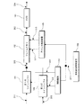
まず、図1に、以下に説明する実施形態における画像表示装置の全体構成を示す。すなわち、画像処理装置1101から出力される信号に基づいて表示器1102に画像が表示される。この画像処理装置1101は、画像信号処理回路であり、以下のそれぞれの実施形態において詳細に説明する。
First, FIG. 1 shows an overall configuration of an image display apparatus according to an embodiment described below. That is, an image is displayed on the
なお、この発明は、大画面表示装置を平置きにして少人数コラボレーションを行うシステムなどに適用して好適なものであり、表示器を平置きにした際に、上下方向から互いに同じ出力画像を見たときに視認性を向上させた反転マルチ表示が可能となる。このような表示器1102としては、例えばCRT、プラズマディスプレイ、液晶ディスプレイ、ELディスプレイ、または電子放出素子を表示素子1102として用いた、フラットパネルディスプレイを用いることができる。なお、表示器1102を平置きするためには、表示器に平置き可能なスタンド等の支持装置が備えられる。なお、平置きとは、表示器1102の表示面の中心における法線が表示器1102を設置する面の法線と交わる角度が30°〜90°となるように、表示器1102が設置されていることをいう。
The present invention is suitable for application to a system that collaborates with a small number of people with a large screen display device placed flat. When the display device is placed flat, the same output images are displayed from the top and bottom. Inverted multi-display with improved visibility when viewed is possible. As such a
(第1の実施形態)
まず、この発明の第1の実施形態による画像処理装置について説明する。図2に、この発明の第1の実施形態による画像処理装置の構成を示す。なお、この第1の実施形態においては、フレームメモリへの画像データの書き込み時または読み込み時にアドレスが制御されて、ライン順反転制御が実行される場合について説明する。
(First embodiment)
First, an image processing apparatus according to a first embodiment of the present invention will be described. FIG. 2 shows the configuration of the image processing apparatus according to the first embodiment of the present invention. In the first embodiment, a case will be described in which an address is controlled when image data is written to or read from a frame memory, and line order inversion control is executed.
図2に示すように、この第1の実施形態による画像処理装置においては、ラインバッファ101、フレームメモリ102、FIFO(First-In First-Out)型バッファ(以下、FIFO)103、反転位置制御装置104、アドレス制御装置105および制御装置107を有して構成されている。第1の実施形態においてラインバッファ101が第1のメモリ部、フレームメモリ102が第2のメモリ部、制御装置107およびアドレス制御装置105が制御回路となる。なお、第1のメモリ部としては、列反転処理が可能なメモリであればよく、またハードウェア規模が小さくなるように容量の小さいメモリが好ましい。このようなメモリとしては、好適には、ラインバッファを用いることができる。
As shown in FIG. 2, in the image processing apparatus according to the first embodiment, a
また、図2中、反転位置制御装置104から制御装置107およびアドレス制御装置105に供給される信号が、列反転位置指示信号S11であり、アドレス制御装置105からフレームメモリ102に供給される信号が、書き込みアドレスS12および読み出しアドレスS13である。また、制御装置107からラインバッファ101に供給される信号が、アドレス指定信号S14である。
In FIG. 2, a signal supplied from the inversion
また、この画像処理装置の内部において入出力されるデータとしては、入力画像データD11、ラインバッファ101から読み出された画像データD12、フレームメモリ102から読み出された画像データD13、およびFIFO103からの出力画像データD14などである。
Data input / output within the image processing apparatus includes input image data D11, image data D12 read from the
これらのデータのうち、入力画像データD11に基づいて、画像表示装置(図示せず)で表示したときの仮想画像を図3Aに示す。このように表示される入力画像データD11は、まず、図2に示すラインバッファ101に供給され、ラインごとに格納される。また、ユーザが外部から列反転位置の情報を入力すると、この列反転位置の情報データが反転位置制御装置104に入力される。このユーザにより設定された列反転位置の情報に基づ
いた列反転位置指示信号S11が制御装置107に供給されることにより、列反転処理のアドレス指定信号S14が、制御装置107からラインバッファ101へ供給される。
Among these data, FIG. 3A shows a virtual image when displayed on an image display device (not shown) based on the input image data D11. The input image data D11 displayed in this way is first supplied to the
次に、アドレス指定信号S14が供給されたラインバッファ101から、あらかじめユーザにより設定された列反転位置まで、画像データが順次カウントアップして出力される。そして、列反転位置になった段階で、ラインバッファ101に順次入力された画像データが、入力順とは逆の順序で出力されるようにラインバッファ101を制御する。すなわち、1ラインの出力画素数から既に出力した画素数を引いた数の位置を基準として、順次カウントダウンされて出力される。
Next, the image data is sequentially counted up and output from the
このようにして、ラインバッファ101から読み出され、フレームメモリ102に供給される画像データD12に基づいて、画像表示装置(図示せず)において表示したときの仮想画像を、図3Bに示す。画像データD12をもとに、仮に画像表示装置で表示するとすれば、ラインバッファ101に入力される画像データに基づいて表示される画像の一部分と、該画像の一部分を画像のラインに対して垂直方向の軸中心で同じ面上に反転させた画像とが表示される。
FIG. 3B shows a virtual image when displayed on an image display device (not shown) based on the image data D12 read from the
実際には、画像データD12がフレームメモリ102に書き込まれるデータとなるため、複数画素転送が行われたり、一旦非同期FIFO(いずれも図示せず)に格納されクロック周波数がアップされたりして、フレームメモリ102に転送される。なお、図3Bにおいては、表示画面のほぼ中央が列反転位置となる場合を例として、この図3B中「Aが示す部分」が入力画像データD11の左側の画像、「Bが示す部分」が左側の画像を列反転させた画像、「Cが示す線」が、反転位置制御装置104から入力された列反転位置情報により決定される反転指示位置を示す。
Actually, since the image data D12 becomes data to be written into the
他方、図2に示すように、列反転位置指示信号S11は、アドレス制御装置105にも供給される。そして、アドレス制御装置105は、フレームメモリ102に入力される複数ライン分の画像信号のうちの一部分が、入力順で出力され、かつ他の部分がライン順が反転されて出力されるようにフレームメモリ102を制御する。すなわち、アドレス制御装置105は、列反転位置指示信号S11に従って、フレームメモリ102への書き込みアドレスS12および読出アドレスS13のいずれか一方のアドレスに対して、列反転位置を基準としてライン順反転処理が実行される。
On the other hand, as shown in FIG. 2, the column inversion position instruction signal S <b> 11 is also supplied to the
次に、入力画像データD11の左上端の座標を(0,0)、右下端の座標を(x,y)
とした場合における、フレームメモリ102から読み出される画像データD13の画素データの並び方の一例を図4および図5に示す。なお、図4および図5中の矢印は、読み出される順番を示す。図4は、フレームメモリ102への書き込み制御時において、ライン順反転処理を実行することなく、読み出しのときにライン順反転処理を行う場合の例である。
Next, the coordinates of the upper left corner of the input image data D11 are (0, 0), and the coordinates of the lower right corner are (x, y).
FIG. 4 and FIG. 5 show an example of how the pixel data of the image data D13 read from the
すなわち、図4に示す画素データの並びに従うと、座標(0,0)の位置から矢印の方向に沿って順次データが読み出され、列反転位置Cに達したところでライン順反転が行われる。他方、図5は、フレームメモリ102への書き込み制御時においてライン順反転処理が実行され、読み出し制御時においてライン順反転処理が実行されない場合の読み出し例を示す。すなわち、座標(0,0)の位置から矢印の方向へ順にデータが読み出され、列反転位置Cに関係なく、そのまま順次データが読み出される。なお、どちらの構成を採用するかは、回路構成によって任意に決定することが可能である。
That is, according to the arrangement of the pixel data shown in FIG. 4, the data is sequentially read from the position of the coordinates (0, 0) along the direction of the arrow, and when the column inversion position C is reached, the line order inversion is performed. On the other hand, FIG. 5 shows an example of reading when the line order inversion process is executed during the write control to the
以上のように、ユーザにより決定され、反転位置制御装置104に入力された列反転位置情報に基づき、その列反転位置において、読み込み制御時または書き込み制御時にライ
ン順反転処理が実行される。そして、フレームメモリ102から読み出された画像データD13は、ラインごとに一旦FIFO103に格納されて、出力のタイミングにあわせて出力されることになる。これにより、画像データD13をもとに、仮に画像表示装置で表示するとすれば、フレームメモリ102に入力される画像データに基づいて表示される画像の一部分と、該画像の一部分を、画像のラインと平行方向の軸を中心に同じ面上に反転した画像とが表示される。
As described above, based on the column inversion position information determined by the user and input to the inversion
そして、出力される出力画像データD14をもとに、画像表示装置(図示せず)において表示されるとすれば、図3Cに示すように、ラインバッファ101に入力される画像データに基づいて表示される画像の一部分が、他の部分に対して同じ面上で回転した状態であって逆の方向に表示される。すなわち、反転マルチ表示とすることが可能となる。
Then, based on the output image data D14 that is output, if it is displayed on an image display device (not shown), the display is based on the image data input to the
(第2の実施形態)
次に、この発明の第2の実施形態による画像処理装置について説明する。図6に、この第2の実施形態による画像処理装置を示す。なお、この第2の実施形態においては、フレームメモリから画像データを読み出す時にライン順反転処理を実行する場合について説明する。
(Second Embodiment)
Next explained is an image processing apparatus according to the second embodiment of the invention. FIG. 6 shows an image processing apparatus according to the second embodiment. In the second embodiment, a case where line order inversion processing is executed when image data is read from the frame memory will be described.
図6に示すように、この第2の実施形態による画像処理装置は、FIFO701、フレームメモリ702、ラインバッファ703、反転位置制御装置704、アドレス制御装置705および制御装置707を有して構成されている。この第2の実施形態においては、第1のメモリ部がラインバッファ703、第2のメモリ部がフレームメモリ702、制御回路が制御装置707およびアドレス制御装置705である。
As shown in FIG. 6, the image processing apparatus according to the second embodiment includes a
また、図6中、外部からFIFO701に入力されるデータが入力画像データD71、このFIFO701から読み出されてフレームメモリ702に供給されるデータが画像データD72、フレームメモリ702から読み出されてラインバッファ703に供給されるデータが画像データD73、および、ラインバッファ703から出力されるデータが出力画像データD74である。また、反転位置制御装置704から列反転位置指示信号S71が出力されて、アドレス制御装置705および制御装置707に供給される。また、アドレス制御装置705から書き込みアドレスS72および読出アドレスS73が出力されて、フレームメモリ702に供給される。また、制御装置707から列反転処理のアドレス指定信号S74が、ラインバッファ703に供給される。
In FIG. 6, data input from the outside to the
まず、外部から供給される入力画像データD71は、ラインごとに一旦FIFO701に格納される。FIFO701からフレームメモリ702の書き込みタイミングに従って読み出された画像データD72が、アドレス制御装置705から出力される書き込みアドレスS72に従ってフレームメモリ702に格納される。
First, input image data D71 supplied from the outside is temporarily stored in the
このフレームメモリ702に格納される画像データとしては、図7に示すデータを一例として挙げることができる。この図7に示す例においては、入力画像データD71の列反転位置Cから左側のデータだけがフレームメモリ702に格納される。フレームメモリ702の列反転位置の右側に格納されるデータは、入力画像データD71の列反転位置の左側のデータを2度読むことによって生成され、フレームメモリ702に格納される。
The image data stored in the
そして、アドレス制御装置705は、フレームメモリ702に入力される複数ライン分の画像信号のうちの一部分が、入力順で出力され、かつ他の部分がライン順が反転されて出力されるようにフレームメモリ702を制御する。すなわち、アドレス制御装置705は、列反転位置指示信号S71に従って、フレームメモリ702への読み出しアドレスS73のアドレスに対して、列反転位置を基準としてライン順反転処理が実行される。
The
これにより、フレームメモリ702から読み出された画像データD73をもとに、仮に画像表示装置で表示するとすれば、フレームメモリ702に入力される画像データに基づいて表示される画像の一部分と、該画像の一部分を、画像のラインと平行方向の軸を中心に同じ面上に反転した画像とが表示される。
Thus, if the image display device displays the image data D73 read from the
図8に、以上のようにして読み出された画像データD73に基づき、画像表示装置(図示せず)において表示する際の仮想画像の一例を示す。図8中「Aが示す部分」が入力画像データD71の左側部分を示し、「Bが示す部分」が入力画像データの左側「Aが示す部分」を縦方向に反転させた画像である。なお、「Cが示す部分」は、ユーザにより設定され、反転位置制御装置704に記憶された列反転位置である。
FIG. 8 shows an example of a virtual image displayed on an image display device (not shown) based on the image data D73 read out as described above. In FIG. 8, “portion indicated by A” indicates the left portion of the input image data D71, and “portion indicated by B” is an image obtained by inverting the left portion “portion indicated by A” of the input image data in the vertical direction. The “part indicated by C” is a column inversion position set by the user and stored in the inversion
そして、フレームメモリ702から読み出された画像データD73が、ラインごとにラインバッファ703に供給されて、格納される。その後、制御装置707から出力されるアドレス指定信号S74により、ラインバッファ703に格納されたデータが、出力のタイミングに従って読み出される。このとき、列反転位置情報を含むアドレス指定信号S74に従って、列反転位置まで画像データを順次カウントアップして出力される。そして列反転位置になった段階で、ラインバッファ703に順次入力された画像データが、入力順とは逆の順序で出力されるようにラインバッファ703を制御する。
The image data D73 read from the
すなわち、1ラインの出力画素数の位置を基準として、列反転位置まで順次カウントダウンされて出力される。以上のように、ラインバッファ703の制御装置により列反転処理が実行され、出力画像データD74が出力される。
That is, the output is sequentially counted down to the column inversion position based on the position of the number of output pixels in one line as a reference. As described above, the column inversion process is executed by the control device of the
そして、出力される出力画像データD74をもとに、画像表示装置において表示されるとすれば、ラインバッファ703に入力される画像データに基づいて表示される画像の一部分と、該画像の一部分を画像のラインに対して垂直方向の軸を中心に反転した画像とが同じ面上に表示される。
Then, if the image is displayed on the image display device based on the output image data D74 that is output, a part of the image displayed based on the image data input to the
以上により、出力される出力画像データD74をもとに、画像表示装置(図示せず)において表示されるとすれば、図3Cに示すように、ラインバッファ101に入力される画像データに基づいて表示される画像の一部分が、他の部分に対して同じ面上で回転した状態であって逆の方向に表示される。すなわち、反転マルチ表示が可能なデータとして出力することが可能となる。
As described above, based on the output image data D74 to be output, if it is displayed on an image display device (not shown), as shown in FIG. 3C, it is based on the image data input to the
(第3の実施形態)
次に、この発明の第3の実施形態による画像処理装置について説明する。図9に、この第3の実施形態による画像処理装置を示す。なお、第1の実施形態におけると同様の構成要素については、同一の符号を付す。また、この第3の実施形態においては、フレームメモリへの画像データの書き込み時においてライン順反転処理を実行する場合について説明する。
(Third embodiment)
Next explained is an image processing apparatus according to the third embodiment of the invention. FIG. 9 shows an image processing apparatus according to the third embodiment. In addition, the same code | symbol is attached | subjected about the component similar to 1st Embodiment. In the third embodiment, a case where line order inversion processing is executed when image data is written to the frame memory will be described.
図9に示すように、この第3の実施形態による画像処理装置は、第1のラインバッファ101、フレームメモリ102およびFIFO103、反転位置制御装置104、アドレス制御装置105、第2のラインバッファ106、および制御装置107を有して構成されている。第3の実施形態においては、第1のラインバッファ101および第2のラインバッファ106が第1のメモリ部、フレームメモリ102が第2のメモリ部、制御装置107とアドレス制御装置105が制御回路である。
As shown in FIG. 9, the image processing apparatus according to the third embodiment includes a
また、図9中、第1の実施形態におけると同様のデータは、外部から第1のラインバッ
ファ101に入力されて格納される第1の入力画像データD11、フレームメモリ102から読み出されてFIFO103に供給される画像データD13および、FIFO103から出力される出力画像データD14である。この第3の実施形態においては、さらに外部から第2の入力画像データD15が第2のラインバッファ106に入力され、第1のラインバッファ101および第2のラインバッファ106から読み出されたデータは、画像データD16としてフレームメモリ102に供給される。
In FIG. 9, the same data as in the first embodiment is read from the first input image data D11 stored in the
また、反転位置制御装置104により、制御装置107およびアドレス制御装置105に供給される列反転位置指示信号S11は、図10中「Cが示す部分」の列反転位置を指示するための命令信号である。また、書き込みアドレスS12、読出アドレスS13およびアドレス指定信号S14、S15に関しては、第1の実施形態におけると同様であるので、その詳細な説明は省略する。
Further, the column inversion position instruction signal S11 supplied from the inversion
まず、第1の入力画像データD11が第1のラインバッファ101に入力されて格納されるとともに、第2の入力画像データD15が第2のラインバッファ106に入力されて格納される。
First, the first input image data D11 is input and stored in the
また、反転位置制御装置104から出力される列反転位置指示信号S11が、制御装置107に、第1のラインバッファ101および第2のラインバッファ106のイネーブルおよび読み出し開始位置が制御される。
Also, the column inversion position instruction signal S11 output from the inversion
すなわち、第1のラインバッファ101の読み出しイネーブルが可の場合には、第2のラインバッファ106の読み出しイネーブルが不可とされる。他方、第1のラインバッファ101の読み出しイネーブルが不可の場合には、第2のラインバッファ106の読み出しイネーブルが可とされる。また、第2のラインバッファ106からの画像データの読み出し時に列反転処理が実行される。
That is, when the read enable of the
具体的には、以下のように第1のラインバッファ101および第2のラインバッファ106から画像データが読み出される。
Specifically, image data is read from the
まず、アドレス指定信号S14が供給された第1のラインバッファ101から、あらかじめユーザにより設定された列反転位置まで画像データが順次カウントアップして出力される。そして、列反転位置になった段階で、アドレス指定信号S15により、第2のラインバッファ106に順次入力された画像データが、入力順とは逆の順序で出力される。すなわち、1ラインの出力画素数から既に出力した画素数を引いた数の位置を基準として、第2のラインバッファ106から画像データが順次カウントダウンされて出力される。
First, image data is sequentially counted up to the column inversion position set in advance by the user from the
このようにして、第1のラインバッファ101からの出力データと第2のラインバッファ106からの出力データとが切り換えられて合成されたデータが画像データD16として、フレームメモリ102に供給される。
In this way, the data synthesized by switching the output data from the
これにより、画像データD16をもとに、仮に画像表示装置で表示するとすれば、第1のラインバッファ101と第2のラインバッファ106に入力された画像データに基づいて表示される画像の一部分と、他の画像の一部分を画像のラインに対して垂直方向の軸を中心に同じ面上に反転した画像とが表示される。
As a result, if the image display device displays the image data D16, a part of the image displayed based on the image data input to the
次に、フレームメモリ102への書き込みは、書き込みアドレスS12によって制御される。また、フレームメモリ102からの読み出しは、読出アドレスS13によって制御される。また、書き込みアドレスS12と読出アドレスS13とは、アドレス制御装置105によって生成される。
Next, writing to the
このアドレス制御装置105により反転位置制御装置104から出力される列反転位置指示信号S11に従って、書き込みアドレスS12におけるライン順反転が実行される。アドレス制御装置105は、フレームメモリ102に入力される複数ライン分の画像信号のうちの一部分が、入力順で出力され、かつ他の部分がライン順が反転されて出力されるようにフレームメモリ102を制御する。
In accordance with the column inversion position instruction signal S11 output from the
すなわち、アドレス制御装置105は、列反転位置指示信号S11に従って、フレームメモリ102への書き込みアドレスS12に対して、列反転位置を基準としてライン順反転処理が実行される。したがって、フレームメモリ102から順次読み出された画像データD13をもとに、仮に画像表示装置で表示するとすれば、フレームメモリ102に入力された画像データに基づいて表示される画像の一部分と、該画像の一部分を、画像のラインと平行方向の軸を中心に同じ面上に反転した画像と、が表示される。
That is, the
そして、フレームメモリ102から読み出された画像データD13は、FIFO103に格納される。続いて、画像データD13がFIFO103に格納された後、画像表示装置(図示せず)のタイミングにあわせて出力画像データD14として出力される。
The image data D13 read from the
出力される出力画像データD14をもとに、仮に画像表示装置(図示せず)で表示するとすれば、第1のラインバッファ101および第2のラインバッファ106に入力される画像データに基づいて表示される画像の一部分が、他の部分に対して同じ面上で回転する方向で逆の方向に表示される。すなわち、反転マルチ表示とすることが可能となる。
If the image is displayed on an image display device (not shown) based on the output image data D14 that is output, the image is displayed based on the image data input to the
ここで、一例として、入力画像データD11に基づいて、画像表示装置(図示せず)で表示したときの仮想画像が図3Aの画像であり、入力画像データD15に基づいて、画像表示装置(図示せず)において表示されたときの仮想画像が図10Aの画像であるとする。このとき、この第3の実施形態による画像処理装置から出力される出力画像データD14に基づいて、不図示の画像表示装置で表示したときの仮想画像は図10Bの画像となる。この図10Bは、それぞれの入力画像データD11,D15をもとにした仮想画像における左端からの表示範囲が設定された例を示す。 Here, as an example, the virtual image when displayed on the image display device (not shown) based on the input image data D11 is the image of FIG. 3A, and based on the input image data D15, the image display device (FIG. It is assumed that the virtual image when displayed in (not shown) is the image of FIG. 10A. At this time, based on the output image data D14 output from the image processing apparatus according to the third embodiment, the virtual image displayed on the image display device (not shown) is the image shown in FIG. 10B. FIG. 10B shows an example in which the display range from the left end in the virtual image based on the respective input image data D11 and D15 is set.
また、この表示範囲の位置は、ユーザにより設定されて外部から入力された反転位置の指示情報データに従って、アドレス制御装置105および制御装置107に設定された表示範囲のデータに応じて、表示範囲を変えることが可能である。
In addition, the position of the display range is determined according to the display range data set in the
以上、この発明の実施形態について具体的に説明したが、この発明は、上述の実施形態に限定されるものではなく、この発明の技術的思想に基づく各種の変形が可能である。 As mentioned above, although embodiment of this invention was described concretely, this invention is not limited to the above-mentioned embodiment, The various deformation | transformation based on the technical idea of this invention is possible.
例えば、上述の実施形態において挙げた数値はあくまでも例に過ぎず、必要に応じてこれと異なる数値を用いてもよい。 For example, the numerical values given in the above embodiment are merely examples, and different numerical values may be used as necessary.
また、例えば上述の第1の実施形態においては、図4および図5において、反転位置Cを、x/2としているが、この反転位置Cの列反転座標はあくまで一例であり、その他の任意の列反転座標を選択することも可能であり、必ずしも全列反転座標の半分(x/2)である必要はない。また、図8および図10Bに示す表示例は、あくまでも説明における一例であり、必ずしも表示画面の中央において反転処理が実行されることを示すものではない。 For example, in the first embodiment described above, in FIG. 4 and FIG. 5, the inversion position C is x / 2, but the column inversion coordinates at the inversion position C are merely an example, and other arbitrary It is also possible to select column inversion coordinates, and it is not always necessary to be half (x / 2) of all column inversion coordinates. Further, the display examples shown in FIGS. 8 and 10B are merely examples in the description, and do not necessarily indicate that the inversion process is performed in the center of the display screen.
また、例えば、上述の実施形態において採用される入力信号としては、インターレース信号とプログレッシブ信号とのいずれの信号であっても良く、必ずしも一方の信号に限定
されるものではない。
For example, the input signal employed in the above-described embodiment may be either an interlace signal or a progressive signal, and is not necessarily limited to one signal.
また、例えば上述の実施形態においては、ラインごとの反転処理について説明したが、必ずしも1ライン毎に限定する趣旨ではなく、隣接する2ラインを同時に走査して画像を表示する方式である、いわゆるラインダブラなどの、複数のラインを走査して画像を表示する方式を採用した場合においても、この発明を適用することができ、同様の効果を得ることができる。 Further, for example, in the above-described embodiment, the inversion processing for each line has been described. However, the inversion processing for each line is not necessarily limited to each line, but a so-called line doubler, which is a method of simultaneously scanning two adjacent lines and displaying an image. The present invention can be applied even when a method of scanning a plurality of lines and displaying an image is used, and the same effect can be obtained.
また、FIFOは、その後段に位置するメモリ部に入力される画像データの転送速度と、メモリ部に画像データを書き込む速度との差を緩和するための一時記憶装置である。したがって、予め画像データの転送速度をメモリ部の画像データ書き込み速度にあわせるように構成すれば、FIFOを必ずしも用いる必要はない。 The FIFO is a temporary storage device for reducing the difference between the transfer speed of image data input to the memory unit located at the subsequent stage and the write speed of image data to the memory unit. Therefore, it is not always necessary to use the FIFO if the image data transfer speed is configured to match the image data writing speed of the memory unit in advance.
101 第1のラインバッファ
102,702 フレームメモリ
103,701 FIFO
104 反転位置制御装置
105 アドレス制御装置
106 第2のラインバッファ
107,707 制御装置
703 ラインバッファ
704 反転位置制御装置
705 アドレス制御装置
D11,D15,D71 入力画像データ
D12,D13,D16 画像データ
D14,D74 出力画像データ
D72,D73 画像データ
S11 列反転位置指示信号
S12,S72 書込アドレス
S13,S73 読出アドレス
S14,S15,S74 アドレス指定信号
S71 列反転位置指示信号
101
104 Reverse
Claims (4)
前記第1のメモリ部から出力される画像信号を複数ライン分格納することが可能な第2のメモリ部と、
前記第1のメモリ部および前記第2のメモリ部を制御する制御回路と、を有し、
前記制御回路は、前記第1のメモリ部にライン単位に格納された画像信号のうち、前記第1のメモリ部の先頭アドレスから任意に設定された列反転位置に対応するアドレスまでの画像信号を前記第1のメモリ部に入力された第1の順序で前記第2のメモリ部に出力した後、前記列反転位置に対応するアドレスから前記先頭アドレスまでの画像信号を前記第1のメモリ部に入力された順序とは逆の第2の順序で出力し、当該出力された画像信号を前記第2のメモリ部に順次入力して複数のライン分の画像信号が格納されるように制御するとともに、前記第2のメモリ部に複数ライン分格納された画像信号のうち、前記第1の順序で前記第1のメモリ部から出力された画像信号は前記第2のメモリ部に入力されたライン順で出力するとともに、前記第2の順序で前記第1のメモリ部から出力された画像信号は前記第2のメモリ部に格納されたライン順とは逆の順序で出力する制御を行う
ことを特徴とする画像信号処理回路。 A first memory unit for storing sequentially input image signals in units of lines;
A second memory unit capable of storing a plurality of lines of image signals output from the first memory unit;
A control circuit for controlling the first memory unit and the second memory unit,
The control circuit outputs image signals from the first address of the first memory unit to an address corresponding to an arbitrarily set column inversion position among the image signals stored in line units in the first memory unit. After outputting to the second memory unit in the first order input to the first memory unit, image signals from the address corresponding to the column inversion position to the head address are input to the first memory unit. The output is performed in a second order opposite to the input order, and the output image signals are sequentially input to the second memory unit to control the image signals for a plurality of lines to be stored. Among the image signals stored in the second memory unit for a plurality of lines, the image signals output from the first memory unit in the first order are the line orders input to the second memory unit. and it outputs in, before Image signal processing circuit image signal output from said first memory portion in a second order which is characterized in that the control output in reverse order of the stored line order in the second memory unit .
前記画像信号処理回路から出力される画像信号に基づいて表示を実行する表示器とを有することを特徴とする画像表示装置。 An image signal processing circuit according to claim 1 ;
An image display apparatus comprising: a display that performs display based on an image signal output from the image signal processing circuit.
前記第1のメモリ部から出力される画像信号を複数ライン分格納することが可能な第2のメモリ部と、
前記第1のメモリ部および前記第2のメモリ部を制御する制御回路と、を有し、
前記制御回路は、前記第1のメモリ部にライン単位に格納された画像信号を出力する際、格納された画像信号のうち、前記第1のメモリ部の先頭アドレスから任意に設定された列反転位置に対応するアドレスまでの画像信号を前記第1のメモリ部に入力された第1の順序で前記第2のメモリ部に出力した後、前記列反転位置に対応するアドレスから前記先頭アドレスまでの画像信号を前記第1のメモリ部に入力された順序とは逆の第2の順序で
前記第2のメモリ部に出力するように制御し、当該出力された画像信号を前記第2のメモリ部にライン単位に複数ライン分格納する際に、前記第1の順序で前記第1のメモリ部から出力された画像信号は前記第2のメモリ部に入力されたライン順で格納するとともに、前記第2の順序で前記第1のメモリ部から出力された画像信号は前記第2のメモリ部に入力されたライン順とは逆の順序で格納する制御を行う
ことを特徴とする画像信号処理回路。 A first memory unit for storing sequentially input image signals in units of lines;
A second memory unit capable of storing a plurality of lines of image signals output from the first memory unit;
A control circuit for controlling the first memory unit and the second memory unit,
When the control circuit outputs the image signal stored in line units to the first memory unit, the column inversion arbitrarily set from the head address of the first memory unit among the stored image signals After the image signal up to the address corresponding to the position is output to the second memory unit in the first order input to the first memory unit, the address from the address corresponding to the column inversion position to the head address controlled so as to output an image signal to the second memory unit in the second order opposite to the order in which they were entered into the first memory portion, wherein the output image signal the second memory section to when storing plural lines in units of lines, along with the image picture signal outputted from the first memory section stores at inputted line order in the second memory unit in the first order, the The first method in a second order; Image signal processing circuit image signal output from the re-section, characterized in that performs control to store in reverse order and are the line order input to the second memory unit.
前記画像信号処理回路から出力される画像信号に基づいて表示を実行する表示器とを有することを特徴とする画像表示装置。
An image signal processing circuit according to claim 3 ,
An image display apparatus comprising: a display that performs display based on an image signal output from the image signal processing circuit.
Priority Applications (1)
| Application Number | Priority Date | Filing Date | Title |
|---|---|---|---|
| JP2005131186A JP4746912B2 (en) | 2004-05-06 | 2005-04-28 | Image signal processing circuit and image display device |
Applications Claiming Priority (3)
| Application Number | Priority Date | Filing Date | Title |
|---|---|---|---|
| JP2004137627 | 2004-05-06 | ||
| JP2004137627 | 2004-05-06 | ||
| JP2005131186A JP4746912B2 (en) | 2004-05-06 | 2005-04-28 | Image signal processing circuit and image display device |
Publications (3)
| Publication Number | Publication Date |
|---|---|
| JP2005346044A JP2005346044A (en) | 2005-12-15 |
| JP2005346044A5 JP2005346044A5 (en) | 2009-09-10 |
| JP4746912B2 true JP4746912B2 (en) | 2011-08-10 |
Family
ID=35498444
Family Applications (1)
| Application Number | Title | Priority Date | Filing Date |
|---|---|---|---|
| JP2005131186A Expired - Fee Related JP4746912B2 (en) | 2004-05-06 | 2005-04-28 | Image signal processing circuit and image display device |
Country Status (1)
| Country | Link |
|---|---|
| JP (1) | JP4746912B2 (en) |
Families Citing this family (4)
| Publication number | Priority date | Publication date | Assignee | Title |
|---|---|---|---|---|
| JP2007334323A (en) * | 2006-05-19 | 2007-12-27 | Semiconductor Energy Lab Co Ltd | Video data control circuit, drive method thereof, and display device and electronic device having video data control circuit |
| JP5213500B2 (en) * | 2008-04-04 | 2013-06-19 | 任天堂株式会社 | Image conversion program and image conversion apparatus |
| KR101653246B1 (en) | 2010-02-03 | 2016-09-12 | 삼성디스플레이 주식회사 | Method of driving a display panel and display apparatus for performing the same |
| CN113299326A (en) * | 2021-05-17 | 2021-08-24 | 珠海市一微半导体有限公司 | FIFO-based data-in-first-out storage circuit and read-write method |
Family Cites Families (1)
| Publication number | Priority date | Publication date | Assignee | Title |
|---|---|---|---|---|
| JP2002251179A (en) * | 2001-02-23 | 2002-09-06 | Sony Tektronix Corp | Device and method for video signal conversion |
-
2005
- 2005-04-28 JP JP2005131186A patent/JP4746912B2/en not_active Expired - Fee Related
Also Published As
| Publication number | Publication date |
|---|---|
| JP2005346044A (en) | 2005-12-15 |
Similar Documents
| Publication | Publication Date | Title |
|---|---|---|
| KR100773850B1 (en) | Image signal processing circuit and image display apparatus | |
| US6914606B2 (en) | Video output controller and video card | |
| JP4746912B2 (en) | Image signal processing circuit and image display device | |
| US20060203002A1 (en) | Display controller enabling superposed display | |
| JP2010081024A (en) | Device for interpolating image | |
| JP2009239899A (en) | Image processing circuit and electronic apparatus having the same circuit | |
| JP2000324337A (en) | Image magnification and reducing device | |
| JP2008116812A (en) | Display apparatus, projector, and display method | |
| JP2005208413A (en) | Image processor and image display device | |
| JP3862976B2 (en) | Display mechanism | |
| US7903175B2 (en) | Device and method for zooming images | |
| JP2010245682A (en) | Image processing device, image processing method, and computer program | |
| JP2005070678A (en) | Image signal processing circuit and mobile terminal device | |
| JP3862983B2 (en) | Display mechanism and computer system | |
| JP2007033759A (en) | Method of displaying image data | |
| JPH05313645A (en) | Image composing and display device | |
| JP2004252009A (en) | Display control method, display control device and display device | |
| KR20220080314A (en) | Video display device including a frame buffer structure for outputting video of a display panel and control method thereof | |
| JPH10274974A (en) | Image display controller | |
| JP2000314869A (en) | Active matrix type liquid crystal display device and display method | |
| JPH0764524A (en) | Image display device | |
| JP2007193159A (en) | Image display controller and image display control method | |
| CN114783363A (en) | Display device and signal control method | |
| JP2007325031A (en) | Image processor, and image processing method | |
| JP2004198930A (en) | Display control method and image display device |
Legal Events
| Date | Code | Title | Description |
|---|---|---|---|
| A521 | Request for written amendment filed |
Free format text: JAPANESE INTERMEDIATE CODE: A523 Effective date: 20070627 |
|
| A621 | Written request for application examination |
Free format text: JAPANESE INTERMEDIATE CODE: A621 Effective date: 20070627 |
|
| A521 | Request for written amendment filed |
Free format text: JAPANESE INTERMEDIATE CODE: A523 Effective date: 20090727 |
|
| A131 | Notification of reasons for refusal |
Free format text: JAPANESE INTERMEDIATE CODE: A131 Effective date: 20100727 |
|
| A521 | Request for written amendment filed |
Free format text: JAPANESE INTERMEDIATE CODE: A523 Effective date: 20100825 |
|
| TRDD | Decision of grant or rejection written | ||
| A01 | Written decision to grant a patent or to grant a registration (utility model) |
Free format text: JAPANESE INTERMEDIATE CODE: A01 Effective date: 20110510 |
|
| A01 | Written decision to grant a patent or to grant a registration (utility model) |
Free format text: JAPANESE INTERMEDIATE CODE: A01 |
|
| A61 | First payment of annual fees (during grant procedure) |
Free format text: JAPANESE INTERMEDIATE CODE: A61 Effective date: 20110516 |
|
| FPAY | Renewal fee payment (event date is renewal date of database) |
Free format text: PAYMENT UNTIL: 20140520 Year of fee payment: 3 |
|
| R150 | Certificate of patent or registration of utility model |
Free format text: JAPANESE INTERMEDIATE CODE: R150 |
|
| LAPS | Cancellation because of no payment of annual fees |