JP5422138B2 - Method for manufacturing semiconductor device - Google Patents
Method for manufacturing semiconductor device Download PDFInfo
- Publication number
- JP5422138B2 JP5422138B2 JP2008094894A JP2008094894A JP5422138B2 JP 5422138 B2 JP5422138 B2 JP 5422138B2 JP 2008094894 A JP2008094894 A JP 2008094894A JP 2008094894 A JP2008094894 A JP 2008094894A JP 5422138 B2 JP5422138 B2 JP 5422138B2
- Authority
- JP
- Japan
- Prior art keywords
- conductive film
- film
- insulating film
- semiconductor device
- antenna
- Prior art date
- Legal status (The legal status is an assumption and is not a legal conclusion. Google has not performed a legal analysis and makes no representation as to the accuracy of the status listed.)
- Expired - Fee Related
Links
Images


Classifications
-
- G—PHYSICS
- G06—COMPUTING; CALCULATING OR COUNTING
- G06K—GRAPHICAL DATA READING; PRESENTATION OF DATA; RECORD CARRIERS; HANDLING RECORD CARRIERS
- G06K19/00—Record carriers for use with machines and with at least a part designed to carry digital markings
- G06K19/06—Record carriers for use with machines and with at least a part designed to carry digital markings characterised by the kind of the digital marking, e.g. shape, nature, code
- G06K19/067—Record carriers with conductive marks, printed circuits or semiconductor circuit elements, e.g. credit or identity cards also with resonating or responding marks without active components
- G06K19/07—Record carriers with conductive marks, printed circuits or semiconductor circuit elements, e.g. credit or identity cards also with resonating or responding marks without active components with integrated circuit chips
- G06K19/077—Constructional details, e.g. mounting of circuits in the carrier
- G06K19/07749—Constructional details, e.g. mounting of circuits in the carrier the record carrier being capable of non-contact communication, e.g. constructional details of the antenna of a non-contact smart card
- G06K19/07773—Antenna details
- G06K19/07775—Antenna details the antenna being on-chip
-
- G—PHYSICS
- G06—COMPUTING; CALCULATING OR COUNTING
- G06K—GRAPHICAL DATA READING; PRESENTATION OF DATA; RECORD CARRIERS; HANDLING RECORD CARRIERS
- G06K19/00—Record carriers for use with machines and with at least a part designed to carry digital markings
- G06K19/06—Record carriers for use with machines and with at least a part designed to carry digital markings characterised by the kind of the digital marking, e.g. shape, nature, code
- G06K19/067—Record carriers with conductive marks, printed circuits or semiconductor circuit elements, e.g. credit or identity cards also with resonating or responding marks without active components
- G06K19/07—Record carriers with conductive marks, printed circuits or semiconductor circuit elements, e.g. credit or identity cards also with resonating or responding marks without active components with integrated circuit chips
- G06K19/077—Constructional details, e.g. mounting of circuits in the carrier
- G06K19/07749—Constructional details, e.g. mounting of circuits in the carrier the record carrier being capable of non-contact communication, e.g. constructional details of the antenna of a non-contact smart card
- G06K19/07773—Antenna details
- G06K19/07777—Antenna details the antenna being of the inductive type
- G06K19/07784—Antenna details the antenna being of the inductive type the inductive antenna consisting of a plurality of coils stacked on top of one another
-
- H—ELECTRICITY
- H01—ELECTRIC ELEMENTS
- H01L—SEMICONDUCTOR DEVICES NOT COVERED BY CLASS H10
- H01L23/00—Details of semiconductor or other solid state devices
- H01L23/52—Arrangements for conducting electric current within the device in operation from one component to another, i.e. interconnections, e.g. wires, lead frames
- H01L23/522—Arrangements for conducting electric current within the device in operation from one component to another, i.e. interconnections, e.g. wires, lead frames including external interconnections consisting of a multilayer structure of conductive and insulating layers inseparably formed on the semiconductor body
- H01L23/5227—Inductive arrangements or effects of, or between, wiring layers
-
- H—ELECTRICITY
- H01—ELECTRIC ELEMENTS
- H01L—SEMICONDUCTOR DEVICES NOT COVERED BY CLASS H10
- H01L23/00—Details of semiconductor or other solid state devices
- H01L23/52—Arrangements for conducting electric current within the device in operation from one component to another, i.e. interconnections, e.g. wires, lead frames
- H01L23/522—Arrangements for conducting electric current within the device in operation from one component to another, i.e. interconnections, e.g. wires, lead frames including external interconnections consisting of a multilayer structure of conductive and insulating layers inseparably formed on the semiconductor body
- H01L23/532—Arrangements for conducting electric current within the device in operation from one component to another, i.e. interconnections, e.g. wires, lead frames including external interconnections consisting of a multilayer structure of conductive and insulating layers inseparably formed on the semiconductor body characterised by the materials
- H01L23/53204—Conductive materials
- H01L23/5328—Conductive materials containing conductive organic materials or pastes, e.g. conductive adhesives, inks
-
- H—ELECTRICITY
- H01—ELECTRIC ELEMENTS
- H01L—SEMICONDUCTOR DEVICES NOT COVERED BY CLASS H10
- H01L23/00—Details of semiconductor or other solid state devices
- H01L23/52—Arrangements for conducting electric current within the device in operation from one component to another, i.e. interconnections, e.g. wires, lead frames
- H01L23/522—Arrangements for conducting electric current within the device in operation from one component to another, i.e. interconnections, e.g. wires, lead frames including external interconnections consisting of a multilayer structure of conductive and insulating layers inseparably formed on the semiconductor body
- H01L23/532—Arrangements for conducting electric current within the device in operation from one component to another, i.e. interconnections, e.g. wires, lead frames including external interconnections consisting of a multilayer structure of conductive and insulating layers inseparably formed on the semiconductor body characterised by the materials
- H01L23/5329—Insulating materials
-
- H—ELECTRICITY
- H01—ELECTRIC ELEMENTS
- H01L—SEMICONDUCTOR DEVICES NOT COVERED BY CLASS H10
- H01L2924/00—Indexing scheme for arrangements or methods for connecting or disconnecting semiconductor or solid-state bodies as covered by H01L24/00
- H01L2924/0001—Technical content checked by a classifier
- H01L2924/0002—Not covered by any one of groups H01L24/00, H01L24/00 and H01L2224/00
Landscapes
- Engineering & Computer Science (AREA)
- Computer Hardware Design (AREA)
- Microelectronics & Electronic Packaging (AREA)
- Physics & Mathematics (AREA)
- General Physics & Mathematics (AREA)
- Theoretical Computer Science (AREA)
- Computer Networks & Wireless Communication (AREA)
- Condensed Matter Physics & Semiconductors (AREA)
- Power Engineering (AREA)
- Internal Circuitry In Semiconductor Integrated Circuit Devices (AREA)
- Thin Film Transistor (AREA)
- Semiconductor Integrated Circuits (AREA)
- Electrodes Of Semiconductors (AREA)
Description
本発明は半導体装置及び当該半導体装置の作製方法に関し、特に非接触で情報の送受信が可能である半導体装置及びその作製方法に関する。 The present invention relates to a semiconductor device and a manufacturing method of the semiconductor device, and more particularly to a semiconductor device capable of transmitting and receiving information without contact and a manufacturing method thereof.
近年、電磁波を無線通信に利用した個体識別技術が注目を集めている。特に、無線通信によりデータの交信を行う半導体装置として、RFID(Radio Frequency Identification)を利用した半導体装置(RFIDタグ、IC(Integrated Circuit)タグ、ICチップ、RFタグ、無線タグ、電子タグとも呼ばれる)による個体識別技術が注目を集めている。RFIDを利用した半導体装置による個体識別技術は、個々の対象物の生産、管理等に役立てられ始めており、個人認証への応用に向けて実用化も進んでいる。 In recent years, individual identification technology using electromagnetic waves for wireless communication has attracted attention. In particular, as a semiconductor device that communicates data by wireless communication, a semiconductor device (RFID tag, IC (Integrated Circuit) tag, IC chip, RF tag, wireless tag, or electronic tag) using RFID (Radio Frequency Identification) is used. The individual identification technology by is attracting attention. Individual identification technology using a semiconductor device using RFID has begun to be used for production, management, etc. of individual objects, and has been put into practical use for application to personal authentication.
このような半導体装置は、リーダ/ライタから受信した電磁波から動作電力を得ると共に、電磁波を利用してリーダ/ライタとの間でデータを交換する。また、半導体装置は、かかる電磁波を送受信するためのアンテナと集積回路部とから構成され、通常、アンテナと集積回路部とは別個に形成された後、接続される。 Such a semiconductor device obtains operating power from electromagnetic waves received from a reader / writer and exchanges data with the reader / writer using the electromagnetic waves. The semiconductor device is composed of an antenna for transmitting and receiving such an electromagnetic wave and an integrated circuit portion. Usually, the antenna and the integrated circuit portion are formed separately and then connected.
アンテナと集積回路部を別個に形成して接続を行う場合、両者を電気的に接続しなければならず、微小な集積回路部の端子とアンテナの接続は技術的困難性を伴うため歩留まりの低下を招いていた。また、半導体装置の使用時に接続点に応力が加わり断線や接続不良の原因となっており、特に可撓性を有する半導体装置を使用する場合には、接続不良が問題となることが予想される。 When the antenna and the integrated circuit part are separately formed and connected, the two must be electrically connected, and the connection between the terminal of the minute integrated circuit part and the antenna is technically difficult, so the yield is reduced. Was invited. In addition, stress is applied to the connection point when using the semiconductor device, causing disconnection or connection failure. In particular, when using a flexible semiconductor device, connection failure is expected to be a problem. .
上述したアンテナと集積回路部の接続不良の問題を解決するべく、集積回路部上にアンテナ(オンチップアンテナ、オンチップコイルとも呼ばれる)が作り込んで設けられた非接触ICモジュールが知られている(例えば、特許文献1)。
しかしながら、集積回路部上にアンテナを作り込んで設ける場合であっても、集積回路部の微細化が進むにつれてアンテナとして機能する導電膜の線幅や形状等も小さくする必要がある。その結果、集積回路部とアンテナとして機能する導電膜の接続不良やコンタクト抵抗が増加するおそれがある。また、集積回路部を多層化する場合、集積回路部とアンテナとして機能する導電膜とを接続する開口部が深くなることにより接続不良が生じる問題がある。 However, even when an antenna is formed over the integrated circuit portion, it is necessary to reduce the line width, shape, and the like of the conductive film functioning as the antenna as the integrated circuit portion is miniaturized. As a result, there is a risk of poor connection and contact resistance between the integrated circuit portion and the conductive film functioning as an antenna. Further, in the case where the integrated circuit portion is multi-layered, there is a problem in that connection failure occurs due to a deep opening that connects the integrated circuit portion and the conductive film functioning as an antenna.
本発明は、上記問題に鑑み、集積回路部上にアンテナを作り込んで設ける場合であっても、接続不良やコンタクト抵抗の増加を抑制することを課題とする。 In view of the above problems, an object of the present invention is to suppress poor connection and increase in contact resistance even when an antenna is formed over an integrated circuit portion.
本発明の半導体装置の一は、基板上に設けられた集積回路部と、集積回路部上に設けられた絶縁膜と、絶縁膜上に設けられたアンテナとして機能する導電膜と、集積回路部とアンテナとして機能する導電膜とを電気的に接続するコンタクト用導電膜とを有し、絶縁膜及びアンテナとして機能する導電膜は開口部を有し、コンタクト用導電膜は、開口部及びアンテナとして機能する導電膜の上面に設けられている。 According to one embodiment of the semiconductor device of the present invention, an integrated circuit portion provided over a substrate, an insulating film provided over the integrated circuit portion, a conductive film functioning as an antenna provided over the insulating film, and the integrated circuit portion And a conductive film for contact electrically connecting the conductive film functioning as an antenna, the conductive film functioning as an insulating film and an antenna has an opening, and the conductive film for contact serves as an opening and an antenna. It is provided on the upper surface of the functional conductive film.
また、本発明の半導体装置の一は、基板上に設けられた集積回路部と、集積回路部上に設けられたアンテナと、集積回路部とアンテナとを電気的に接続するコンタクト用導電膜とを有し、アンテナは、複数の導電膜がそれぞれ絶縁膜を介して積層して設けられており、複数の導電膜及び絶縁膜は開口部を有し、コンタクト用導電膜は、開口部に設けられている。 According to another aspect of the semiconductor device of the present invention, an integrated circuit portion provided over a substrate, an antenna provided over the integrated circuit portion, a contact conductive film that electrically connects the integrated circuit portion and the antenna, The antenna includes a plurality of conductive films stacked via an insulating film, the plurality of conductive films and the insulating film have openings, and the contact conductive film is provided in the openings. It has been.
また、本発明の半導体装置の作製方法の一は、基板上に第1の導電膜を有する集積回路部を形成し、集積回路部上に絶縁膜を形成し、絶縁膜上にアンテナとして機能する第2の導電膜を形成し、絶縁膜及び第2の導電膜に開口部を形成して第1の導電膜を露出させ、めっき処理により開口部及び第2の導電膜の上面に第3の導電膜を形成することにより、第1の導電膜と第2の導電膜とを電気的に接続する。 In one embodiment of the method for manufacturing a semiconductor device of the present invention, an integrated circuit portion having a first conductive film is formed over a substrate, an insulating film is formed over the integrated circuit portion, and the semiconductor device functions as an antenna over the insulating film. A second conductive film is formed, an opening is formed in the insulating film and the second conductive film to expose the first conductive film, and a third treatment is performed on the upper surface of the opening and the second conductive film by plating. By forming the conductive film, the first conductive film and the second conductive film are electrically connected.
また、本発明の半導体装置の作製方法の一は、基板上に第1の導電膜を有する集積回路部を形成し、集積回路部上に第1の絶縁膜を形成し、第1の絶縁膜上にアンテナとして機能する複数の第2の導電膜を第2の絶縁膜を介して積層させて形成し、第1の絶縁膜、第2の導電膜及び第2の絶縁膜に開口部を形成して第1の導電膜を露出させ、めっき処理により開口部に第3の導電膜を形成することにより、第1の導電膜と複数の第2の導電膜とを電気的に接続する。 According to another method for manufacturing a semiconductor device of the present invention, an integrated circuit portion having a first conductive film is formed over a substrate, a first insulating film is formed over the integrated circuit portion, and the first insulating film is formed. A plurality of second conductive films functioning as antennas are stacked over the second insulating film, and openings are formed in the first insulating film, the second conductive film, and the second insulating film. Then, the first conductive film is exposed, and a third conductive film is formed in the opening by plating, thereby electrically connecting the first conductive film and the plurality of second conductive films.
本発明により、集積回路部上にアンテナを作り込んで設ける場合においても、接続不良やコンタクト抵抗の増加を抑制することが可能となる。 According to the present invention, even when an antenna is formed over an integrated circuit portion, it is possible to suppress connection failure and increase in contact resistance.
以下、本発明の実施の形態について図面を参照しながら説明する。ただし、本発明は多くの異なる態様で実施することが可能であり、本発明の趣旨及びその範囲から逸脱することなくその形態及び詳細を様々に変更し得ることは当業者であれば容易に理解される。したがって、本実施の形態の記載内容に限定して解釈されるものではない。なお、本明細書中の図面において、同一部分または同様な機能を有する部分には同一の符号を付し、その説明は省略する場合がある。 Hereinafter, embodiments of the present invention will be described with reference to the drawings. However, the present invention can be implemented in many different modes, and those skilled in the art can easily understand that the modes and details can be variously changed without departing from the spirit and scope of the present invention. Is done. Therefore, the present invention is not construed as being limited to the description of this embodiment mode. Note that in the drawings in this specification, the same portions or portions having similar functions are denoted by the same reference numerals, and description thereof may be omitted.
(実施の形態1)
本実施の形態では、本発明の半導体装置の一例に関し図面を参照して説明する。なお、以下の説明において、図1は半導体装置の上面を示しており、図2は図1のA1−B1間の断面図を示している。
(Embodiment 1)
In this embodiment, an example of a semiconductor device of the present invention will be described with reference to drawings. In the following description, FIG. 1 shows the top surface of the semiconductor device, and FIG. 2 shows a cross-sectional view between A 1 and B 1 in FIG.
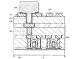
本実施の形態で示す半導体装置は、基板101上に設けられた集積回路部102と、アンテナとして機能する導電膜103と、集積回路部102と導電膜103とを電気的に接続する導電膜104とを有している(図1、図2参照)。
The semiconductor device described in this embodiment includes an
アンテナとして機能する導電膜103は、集積回路部102の上方に絶縁膜106を介して設けられており、集積回路部102と導電膜103とが一部又は全部重なった構成とすることができる。また、集積回路部102とアンテナとして機能する導電膜103との電気的な接続は、絶縁膜106及び導電膜103に形成された開口部107を介して導電膜104により行われる。つまり、導電膜104は、集積回路部102と導電膜103のコンタクト用導電膜として機能しうる。なお、本実施の形態で示す半導体装置は、アンテナとして機能する導電膜が集積回路部上に直接作り込んで設けられた構成(オンチップアンテナ)となっている。
The
集積回路部102は、トランジスタ等の素子110、配線として機能しうる導電膜105等が設けられた構成とすることができる。
The
また、導電膜104は、開口部107の近傍における導電膜103の上面にも形成する。このように、導電膜103の側面及び上面と接するように導電膜104を形成することによって、導電膜104と導電膜103の接触面積が大きくなるため、アンテナとして機能する導電膜103と集積回路部102の接触不良の低減やコンタクト抵抗を下げることができる。
The
導電膜104は、めっき処理を用いて形成することが好ましい。集積回路部102の多層化等により開口部107が深く設けられた場合であっても、めっき処理により導電膜104を形成することによって、開口部107の底まで十分に導電膜104を設けることが可能となる。その結果、導電膜104と導電膜105との接続不良を抑制し、コンタクト抵抗を下げることができる。
The
一般的に、開口部107を形成後、アンテナとして機能する導電膜103をCVD法、スパッタリング法、スクリーン印刷法、液滴吐出法等で形成して、直接集積回路部102と電気的に接続する場合には、開口部107の底部に十分導電膜が形成されず接続不良やコンタクト抵抗が増加するおそれがある。しかし、集積回路部102及びアンテナとして機能する導電膜103を形成した後、開口部107を設けコンタクト用導電膜として機能する導電膜105をめっき処理により形成することにより、導電膜103と集積回路部102との接続不良を抑制し、コンタクト抵抗を下げることができる。
In general, after the
具体的には、めっき処理により導電膜104を、銅(Cu)、ニッケル(Ni)、金(Au)、白金(Pt)、銀(Ag)、コバルト(Co)、錫(Sn)から選択された元素、又はこれらの元素を主成分とする合金材料若しくは化合物材料で、単層構造又は積層構造で設けることができる。
Specifically, the
なお、上記図1、図2に示した半導体装置では、アンテナとして機能する導電膜103及び絶縁膜106に開口部107を形成した構成としたが、本実施の形態で示す半導体装置はこれに限られない。例えば、アンテナとして機能する導電膜103を形成した後、絶縁膜106に開口部107を形成し、アンテナとして機能する導電膜103には開口部を形成しない構成としてもよい(図3、図4参照)。この場合、アンテナとして機能する導電膜103の上面及び側面と接するように導電膜104を設けることにより、接触不良の低減やコンタクト抵抗を下げることができる。
Note that although the semiconductor device illustrated in FIGS. 1 and 2 has the structure in which the
なお、本実施の形態で示した半導体装置において、アンテナとして機能する導電膜103と重なるようにブースターアンテナを設けた構成としてもよい。ブースターアンテナを設けることによって、導電膜103を小さくする場合であっても、通信距離の低下を抑制することができる。
Note that in the semiconductor device described in this embodiment, a booster antenna may be provided so as to overlap with the
次に、上述した半導体装置の作製方法に関し図面を参照して以下に説明する。 Next, a method for manufacturing the semiconductor device described above will be described below with reference to the drawings.
まず、基板101上にトランジスタ等を含む素子110、配線として機能しうる導電膜105が設けられた集積回路部102を形成する(図5(A)参照)。
First, the
基板101は、例えば、単結晶基板、SOI基板、ガラス基板、石英基板、金属基板やステンレス基板、プラスチック基板等を用いることができる。
As the
集積回路部102に設けられるトランジスタは、様々な形態のトランジスタを適用させることができる。例えば、非晶質シリコンや多結晶シリコンに代表される非単結晶半導体膜を用いた薄膜トランジスタ(TFT)、半導体基板やSOI基板を用いて形成されるトランジスタ、MOS型トランジスタ、接合型トランジスタ、バイポーラトランジスタ、ZnO、a−InGaZnOなどの化合物半導体を用いたトランジスタ、有機半導体やカーボンナノチューブを用いたトランジスタ、その他のトランジスタを適用することができる。なお、非単結晶半導体膜には水素またはハロゲンが含まれていてもよい。
Various types of transistors can be used as the transistor provided in the
また、トランジスタの構成は、様々な形態をとることができる。特定の構成に限定されない。例えば、ゲート本数が2本以上になっているマルチゲート構造を用いてもよい。マルチゲート構造にすることにより、オフ電流の低減や、トランジスタの耐圧を向上させて信頼性を良くし、飽和領域で動作する時に、ドレインとソース間電圧が変化しても、ドレインとソース間電流があまり変化せず、フラットな特性にすることができる。また、LDD領域があってもよい。LDD領域を設けることにより、オフ電流の低減や、トランジスタの耐圧を向上させて信頼性を良くし、飽和領域で動作する時に、ドレインとソース間電圧が変化しても、ドレインとソース間電流があまり変化せず、フラットな特性にすることができる。 In addition, the structure of the transistor can take a variety of forms. It is not limited to a specific configuration. For example, a multi-gate structure having two or more gates may be used. The multi-gate structure reduces off-current, improves the breakdown voltage of the transistor to improve reliability, and even when the drain-source voltage changes when operating in the saturation region, the drain-source current Does not change so much, and a flat characteristic can be obtained. There may also be an LDD region. By providing the LDD region, the off-current is reduced and the breakdown voltage of the transistor is improved to improve the reliability. When operating in the saturation region, the drain-source current does not change even if the drain-source voltage changes. It does not change so much and can be made flat.
次に、集積回路部102を覆うように絶縁膜106を形成し、当該絶縁膜106上に導電膜103を選択的に形成する。その後、導電膜103を覆うように絶縁膜109を形成する(図5(B)参照)。なお、導電膜103は、半導体装置においてアンテナとして機能する。
Next, an insulating
絶縁膜106、絶縁膜109は、CVD法、スパッタ法、SOG法、液滴吐出法、スクリーン印刷法等により、シリコンの酸化物やシリコンの窒化物等の無機材料(例えば、酸化珪素(SiOx)、酸化窒化珪素(SiOxNy)(x>y)、窒化珪素(SiNx)、窒化酸化珪素(SiNxOy)(x>y)等)、ポリイミド、ポリアミド、ベンゾシクロブテン、アクリル、エポキシ等の有機材料やシロキサン材料等により、単層または積層で形成する。絶縁膜106と絶縁膜109は同一の材料で形成してもよいし、異なる材料で形成してもよい。なお、シロキサン材料とは、Si−O−Si結合を含む材料に相当する。シロキサンは、シリコン(Si)と酸素(O)との結合で骨格構造が構成される。置換基として、少なくとも水素を含む有機基(例えばアルキル基、芳香族炭化水素)が用いられる。置換基として、フルオロ基を用いることもできる。または置換基として、少なくとも水素を含む有機基と、フルオロ基とを用いてもよい。
The insulating
導電膜103は、CVD法、スパッタリング法、スクリーン印刷やグラビア印刷等の印刷法、液滴吐出法、めっき処理等を用いて、導電性材料により形成する。導電性材料は、アルミニウム(Al)、チタン(Ti)、銀(Ag)、銅(Cu)、金(Au)、白金(Pt)ニッケル(Ni)、パラジウム(Pd)、タンタル(Ta)、モリブデン(Mo)から選択された元素、又はこれらの元素を主成分とする合金材料若しくは化合物材料で、単層構造又は積層構造で形成する。
The
例えば、スクリーン印刷法を用いてアンテナとして機能する導電膜103を形成する場合には、粒径が数nmから数十μmの導電体粒子を有機樹脂に溶解または分散させた導電性のペーストを選択的に印刷することによって設けることができる。導電体粒子としては、銀(Ag)、金(Au)、銅(Cu)、ニッケル(Ni)、白金(Pt)、パラジウム(Pd)、タンタル(Ta)、モリブデン(Mo)およびチタン(Ti)等のいずれか一つ以上の金属粒子やハロゲン化銀の微粒子、または分散性ナノ粒子を用いることができる。スクリーン印刷法を用いて形成することにより、工程の簡略化が可能となり低コスト化を図ることができる。
For example, when the
次に、絶縁膜106、導電膜103及び絶縁膜109の一部を選択的に除去して、開口部107を形成する(図6(A)参照)。開口部107は、集積回路部102に設けられた導電膜105の少なくとも一部が露出するように設ける。また、開口部107の近傍における導電膜103の上面が露出するように、絶縁膜109をエッチングする。
Next, part of the insulating
次に、開口部107及び導電膜103の表面にシード層111を形成する(図6(B)参照)。
Next, a
シード層は、スパッタリング法、CVD法等により、銅(Cu)、ニッケル(Ni)、クロム(Cr)等で形成することができる。なお、シード層111の形成前にバリア層としてタンタル(Ta)、窒化タンタル、チタン(Ti)、窒化チタン等をあらかじめ形成してもよい。他にも、露出している絶縁膜106、絶縁膜109等の表面に粗化処理を施して表面に凹凸を形成した後に、無電解めっきで銅(Cu)を形成することにより設けてもよい。
The seed layer can be formed of copper (Cu), nickel (Ni), chromium (Cr), or the like by a sputtering method, a CVD method, or the like. Note that tantalum (Ta), tantalum nitride, titanium (Ti), titanium nitride, or the like may be formed in advance as a barrier layer before the
次に、開口部107及び当該開口部107近傍の導電膜103の上面に導電膜104を選択的に形成する(図7参照)。その結果、集積回路部102とアンテナとして機能する導電膜103が導電膜104を介して電気的に接続される。
Next, the
導電膜104は、めっき処理により、銅(Cu)、ニッケル(Ni)、金(Au)、白金(Pt)、銀(Ag)、コバルト(Co)、錫(Sn)から選択された元素、又はこれらの元素を主成分とする合金材料若しくは化合物材料で、単層構造又は積層構造で形成する。具体的には、めっき処理によりシード層111上に導電膜を形成した後、当該導電膜及びシード層を選択的に除去することによりコンタクト用導電膜となる導電膜104を形成する。
The
めっき処理により導電膜104を設けることにより、開口部107の底まで十分に導電膜104を設けることが可能となるため、導電膜104と導電膜105との接続不良を抑制し、コンタクト抵抗を下げることができる。
By providing the
なお、本実施の形態で示す半導体装置の作製方法において、アディティブ法又はセミアディティブ法を適用して導電膜104の形成してもよい。
Note that in the method for manufacturing a semiconductor device described in this embodiment, the
本実施の形態で示したように、集積回路部上に絶縁膜を介してアンテナとして機能する導電膜を設けた後に、絶縁膜及びアンテナとして機能する導電膜に開口部を設け、当該開口部及びアンテナとして機能する導電膜の上面にコンタクト用導電膜を形成して集積回路部とアンテナとして機能する導電膜とを電気的に接続することにより、接触不良の低減やコンタクト抵抗を低減することができる。また、開口部が深い場合であっても、めっき処理によりコンタクト用の導電膜を形成することにより接続不良を抑制することができる。 As described in this embodiment, after a conductive film functioning as an antenna is provided over an integrated circuit portion with an insulating film interposed therebetween, an opening portion is provided in the insulating film and the conductive film functioning as an antenna. By forming a contact conductive film on the upper surface of the conductive film functioning as an antenna and electrically connecting the integrated circuit portion and the conductive film functioning as an antenna, contact failure can be reduced and contact resistance can be reduced. . Even when the opening is deep, connection failure can be suppressed by forming a conductive film for contact by plating.
本実施の形態は、本明細書の他の実施の形態で示した半導体装置の構成と自由に組み合わせて実施することができる。 This embodiment can be implemented in free combination with the structures of the semiconductor devices described in the other embodiments in this specification.
(実施の形態2)
本実施の形態では、上記実施の形態と異なる構成の半導体装置に関して、図面を参照して説明する。
(Embodiment 2)
In this embodiment, a semiconductor device having a structure different from that of the above embodiment is described with reference to drawings.
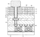
本実施の形態で示す半導体装置は、基板101上に設けられた集積回路部102と、アンテナとして機能する複数の導電膜103と、集積回路部102と導電膜103とを電気的に接続する導電膜104とを有している(図8参照)。アンテナとして機能する複数の導電膜103は、絶縁膜121を介して積層して設けられており、複数の導電膜103はそれぞれ導電膜104と電気的に接続されている。つまり、上記図2で示した構成と比較して、複数の導電膜103を積層構造で設けた点で相違している。
In the semiconductor device described in this embodiment, an
絶縁膜121は、CVD法、スパッタリング法、SOG法、液滴吐出法、スクリーン印刷法等により、シリコンの酸化物やシリコンの窒化物等の無機材料(例えば、酸化珪素、酸化窒化珪素、窒化珪素、窒化酸化珪素等)、ポリイミド、ポリアミド、ベンゾシクロブテン、アクリル、エポキシ等の有機材料やシロキサン材料等により、単層または積層で形成する。
The insulating
また、絶縁膜121は、導電膜103に酸化処理と窒化処理の一方又は両方を行うことにより形成してもよい。例えば、導電膜103として、アルミニウム(Al)を用いた場合、当該アルミニウムを酸化又は窒化することにより、絶縁膜121を酸化アルミニウム(AlOx)又は窒化アルミニウム(AlNx)で設けた構成とすることができる。また、絶縁膜121と絶縁膜109を同一の材料で設けてもよい。
Alternatively, the insulating
このようにアンテナとして機能する複数の導電膜103を積層して設けることにより、表皮効果の影響を低減することができる。つまり、アンテナとして機能する導電膜103の抵抗を下げるために膜厚を厚く設けた場合、導電膜103に流れる電流が表皮効果により導電膜103の表面に集中するため、結果的に抵抗を十分に下げることができない。しかし、アンテナとして機能する導電膜103を絶縁膜121を介して積層させた構成とすることにより、複数の導電膜103の表面にそれぞれ電流が流れるため、表皮効果の影響を低減することが可能となる。
By providing the plurality of
また、複数の導電膜103を積層して設けた場合であっても、絶縁膜106、導電膜103及び絶縁膜121に開口部107を設け、当該開口部107にコンタクト用導電膜として機能しうる導電膜104を設けることにより、導電膜103と導電膜105との接続不良を抑制し、コンタクト抵抗を下げることができる。さらに、複数の導電膜103を設けた後に導電膜104を用いて一工程で集積回路部102と複数の導電膜103との電気的な接続を行うため、工程を簡略化することができる。
Further, even when the plurality of
また、複数の導電膜103を積層して設ける場合には、開口部107が深くなるが、めっき処理により導電膜104を設けることにより開口部107の底まで十分に導電膜104を設けることが可能となる。その結果、アンテナとして機能する複数の導電膜103を積層して設けた場合であっても、導電膜104と導電膜105との接続不良を抑制し、コンタクト抵抗を下げることができる。
In the case where a plurality of
なお、上述した半導体装置の構成は、アンテナとして機能する導電膜103をコイル状に設けた電磁誘導方式に関するものであるが、これに限られない。アンテナとして機能する導電膜103は様々な形状で設けることが可能である。
Note that the structure of the semiconductor device described above relates to an electromagnetic induction method in which the
例えば、アンテナとして機能する導電膜103を線状として設けてもよい(図9(A)、(B)参照)。このように、本実施の形態又は上記実施の形態で示す構造はアンテナの形状に限られず適用することができる。なお、図9(A)は半導体装置の上面を示し、図9(B)は図9(A)におけるA2−B2間の断面図を示している。
For example, the
本実施の形態は、本明細書の他の実施の形態で示した半導体装置の構成又は作製方法と自由に組み合わせて実施することができる。 This embodiment can be implemented freely combining with the structure or manufacturing method of the semiconductor device described in any of the other embodiments in this specification.
(実施の形態3)
本実施の形態では、上記実施の形態で示した半導体装置の作製方法の一例に関して、図面を参照して説明する。本実施の形態においては、半導体装置の集積回路部に含まれる素子等を同一基板上に薄膜トランジスタを用いて設ける場合について説明する。なお、本実施の形態では、薄膜トランジスタ等の素子を一度支持基板に設けた後、可撓性を有する基板に転置して半導体装置を作製する場合に関して説明する。また、本実施の形態では、一つの基板に複数の集積回路部及びアンテナを形成し(ここでは、縦4×横3)、複数の半導体装置を作製する場合について説明する。以下の説明において、図12、図13は上面図の模式図であり、図14〜図18は図12〜図13におけるA−B間の断面図の模式図である。
(Embodiment 3)
In this embodiment, an example of a method for manufacturing the semiconductor device described in the above embodiment is described with reference to drawings. In this embodiment, the case where an element included in an integrated circuit portion of a semiconductor device is provided using a thin film transistor over the same substrate will be described. Note that in this embodiment, a case where a device such as a thin film transistor is provided over a supporting substrate and then transferred to a flexible substrate to manufacture a semiconductor device will be described. In this embodiment, a case where a plurality of integrated circuit portions and antennas are formed over one substrate (here, 4 × 3 in width) to manufacture a plurality of semiconductor devices is described. In the following description, FIGS. 12 and 13 are schematic diagrams of top views, and FIGS. 14 to 18 are schematic diagrams of cross-sectional views between A and B in FIGS. 12 to 13.
まず、基板1601の一表面に剥離層1602を形成し、続けて下地となる絶縁膜1603および非晶質半導体膜1604(例えば非晶質珪素を含む膜)を形成する(図12(A)、図14(A))。剥離層1602、絶縁膜1603および非晶質半導体膜1604は、連続して形成することができる。連続して形成することにより、大気に曝されないため不純物の混入を防ぐことができる。なお、以下の工程において、図12(A)に示された複数の領域1650にそれぞれ半導体装置を構成する集積回路部及びアンテナが形成される。
First, a
基板1601は、ガラス基板、石英基板、金属基板やステンレス基板、本工程の処理温度に耐えうる耐熱性があるプラスチック基板等を用いるとよい。このような基板であれば、その面積や形状に大きな制限はないため、例えば、1辺が1メートル以上であって、矩形状のものを用いれば、生産性を格段に向上させることができる。このような利点は、円形のシリコン基板を用いる場合と比較すると、大きな優位点である。従って、シリコン基板と比較して集積回路部やアンテナを大きく形成した場合であっても、低コスト化を実現することができる。
As the
なお、本工程では、剥離層1602を基板1601の全面に設けているが、必要に応じて、基板1601の全面に剥離層を設けた後に、フォトリソグラフィ法により剥離層1602を選択的に設けてもよい。また、基板1601に接するように剥離層1602を形成しているが、必要に応じて、基板1601に接するように酸化珪素(SiOx)膜、酸化窒化珪素(SiOxNy)(x>y)膜、窒化珪素(SiNx)膜、窒化酸化珪素(SiNxOy)(x>y)膜等の絶縁膜を形成し、当該絶縁膜に接するように剥離層1602を形成してもよい。
Note that although the
剥離層1602は、金属膜や金属膜と金属酸化膜の積層構造等を用いることができる。金属膜としては、タングステン(W)、モリブデン(Mo)、チタン(Ti)、タンタル(Ta)、ニオブ(Nb)、ニッケル(Ni)、コバルト(Co)、ジルコニウム(Zr)、亜鉛(Zn)、ルテニウム(Ru)、ロジウム(Rh)、パラジウム(Pd)、オスミウム(Os)、イリジウム(Ir)から選択された元素または前記元素を主成分とする合金材料若しくは化合物材料からなる膜を単層又は積層して形成する。また、これらの材料は、スパッタリング法やプラズマCVD法等の各種CVD法等を用いて形成することができる。金属膜と金属酸化膜の積層構造としては、上述した金属膜を形成した後に、酸素雰囲気化またはN2O雰囲気下におけるプラズマ処理、酸素雰囲気化またはN2O雰囲気下における加熱処理を行うことによって、金属膜表面に当該金属膜の酸化物または酸化窒化物を設けることができる。また、金属膜を形成した後に、オゾン水等の酸化力の強い溶液で表面を処理することにより、金属膜表面に当該金属膜の酸化物又は酸化窒化物を設けることができる。
The
絶縁膜1603は、スパッタリング法やプラズマCVD法等により、珪素の酸化物または珪素の窒化物を含む膜を、単層又は積層で形成する。下地となる絶縁膜が2層構造の場合、例えば、1層目として窒化酸化珪素膜を形成し、2層目として酸化窒化珪素膜を形成するとよい。下地となる絶縁膜が3層構造の場合、1層目の絶縁膜として酸化珪素膜を形成し、2層目の絶縁膜として窒化酸化珪素膜を形成し、3層目の絶縁膜として酸化窒化珪素膜を形成するとよい。または、1層目の絶縁膜として酸化窒化珪素膜を形成し、2層目の絶縁膜として窒化酸化珪素膜を形成し、3層目の絶縁膜として酸化窒化珪素膜を形成するとよい。下地となる絶縁膜は、基板1601からの不純物の侵入を防止するブロッキング膜として機能する。
The insulating
半導体膜1604は、スパッタリング法、LPCVD法、プラズマCVD法等により、25〜200nm(好ましくは30〜150nm)の厚さで形成する。半導体膜1604としては、例えば、非晶質珪素膜を形成すればよい。
The
次に、非晶質の半導体膜1604にレーザー光を照射して結晶化を行う。なお、レーザー光の照射と、RTA又はファーネスアニール炉を用いる熱結晶化法、結晶化を助長する金属元素を用いる熱結晶化法とを組み合わせた方法等により非晶質の半導体膜1604の結晶化を行ってもよい。その後、得られた結晶質半導体膜を所望の形状にエッチングして、半導体膜1604a〜1604dを形成し、当該半導体膜1604a〜1604dを覆うようにゲート絶縁膜1605を形成する(図14(B))。
Next, crystallization is performed by irradiating the
半導体膜1604a〜1604dの作製工程の一例を以下に簡単に説明すると、まず、プラズマCVD法を用いて、膜厚50〜60nmの非晶質半導体膜(例えば、非晶質珪素膜)を形成する。次に、結晶化を助長する金属元素であるニッケルを含む溶液を非晶質半導体膜上に保持させた後、非晶質半導体膜に脱水素化の処理(500℃、1時間)と、熱結晶化の処理(550℃、4時間)を行って結晶質半導体膜を形成する。その後、レーザー発振器からレーザー光を照射し、フォトリソグラフィ法を用いることによって半導体膜1604a〜1604dを形成する。なお、結晶化を助長する金属元素を用いる熱結晶化を行わずに、レーザー光の照射だけで非晶質半導体膜の結晶化を行ってもよい。
An example of a manufacturing process of the
レーザー発振器としては、連続発振型のレーザービーム(CWレーザービーム)やパルス発振型のレーザービーム(パルスレーザービーム)を用いることができる。ここで用いることができるレーザービームは、Arレーザー、Krレーザー、エキシマレーザーなどの気体レーザー、単結晶のYAG、YVO4、フォルステライト(Mg2SiO4)、YAlO3、GdVO4、若しくは多結晶(セラミック)のYAG、Y2O3、YVO4、YAlO3、GdVO4に、ドーパントとしてNd、Yb、Cr、Ti、Ho、Er、Tm、Taのうち1種または複数種添加されているものを媒質とするレーザー、ガラスレーザー、ルビーレーザー、アレキサンドライトレーザー、Ti:サファイアレーザー、銅蒸気レーザーまたは金蒸気レーザーのうち一種または複数種から発振されるものを用いることができる。このようなレーザービームの基本波、及びこれらの基本波の第2高調波から第4高調波のレーザービームを照射することで、大粒径の結晶を得ることができる。例えば、Nd:YVO4レーザー(基本波1064nm)の第2高調波(532nm)や第3高調波(355nm)を用いることができる。このときレーザーのパワー密度は0.01〜100MW/cm2程度(好ましくは0.1〜10MW/cm2)が必要である。そして、走査速度を10〜2000cm/sec程度として照射する。なお、単結晶のYAG、YVO4、フォルステライト(Mg2SiO4)、YAlO3、GdVO4、若しくは多結晶(セラミック)のYAG、Y2O3、YVO4、YAlO3、GdVO4に、ドーパントとしてNd、Yb、Cr、Ti、Ho、Er、Tm、Taのうち1種または複数種添加されているものを媒質とするレーザー、Arイオンレーザー、またはTi:サファイアレーザーは、連続発振をさせることが可能であり、Qスイッチ動作やモード同期などを行うことによって10MHz以上の発振周波数でパルス発振をさせることも可能である。10MHz以上の発振周波数でレーザービームを発振させると、半導体膜がレーザーによって溶融してから固化するまでの間に、次のパルスが半導体膜に照射される。従って、発振周波数が低いパルスレーザーを用いる場合と異なり、半導体膜中において固液界面を連続的に移動させることができるため、走査方向に向かって連続的に成長した結晶粒を得ることができる。 As the laser oscillator, a continuous wave laser beam (CW laser beam) or a pulsed laser beam (pulse laser beam) can be used. The laser beam that can be used here is a gas laser such as Ar laser, Kr laser, or excimer laser, single crystal YAG, YVO 4 , forsterite (Mg 2 SiO 4 ), YAlO 3 , GdVO 4 , or polycrystalline ( (Ceramics) YAG, Y 2 O 3 , YVO 4 , YAlO 3 , GdVO 4 with one or more of Nd, Yb, Cr, Ti, Ho, Er, Tm, Ta added as dopants Lasers oscillated from one or more of laser, glass laser, ruby laser, alexandrite laser, Ti: sapphire laser, copper vapor laser or gold vapor laser as a medium can be used. By irradiating the fundamental wave of such a laser beam and the second to fourth harmonics of these fundamental waves, a crystal having a large grain size can be obtained. For example, the second harmonic (532 nm) or the third harmonic (355 nm) of an Nd: YVO 4 laser (fundamental wave 1064 nm) can be used. In this case, a laser power density is about 0.01 to 100 MW / cm 2 (preferably 0.1 to 10 MW / cm 2) is required. Then, irradiation is performed at a scanning speed of about 10 to 2000 cm / sec. Note that single crystal YAG, YVO 4 , forsterite (Mg 2 SiO 4 ), YAlO 3 , GdVO 4 , or polycrystalline (ceramic) YAG, Y 2 O 3 , YVO 4 , YAlO 3 , GdVO 4 , dopants Nd, Yb, Cr, Ti, Ho, Er, Tm, Ta as a medium, a laser, Ar ion laser, or Ti: sapphire laser with one or more added as a medium should be continuously oscillated It is also possible to perform pulse oscillation at an oscillation frequency of 10 MHz or more by performing Q switch operation, mode synchronization, or the like. When a laser beam is oscillated at an oscillation frequency of 10 MHz or higher, the semiconductor film is irradiated with the next pulse during the period from when the semiconductor film is melted by the laser to solidification. Therefore, unlike the case of using a pulse laser having a low oscillation frequency, the solid-liquid interface can be continuously moved in the semiconductor film, so that crystal grains continuously grown in the scanning direction can be obtained.
次に、半導体膜1604a〜半導体膜1604dを覆うゲート絶縁膜1605を形成する。ゲート絶縁膜1605は、CVD法やスパッタリング法等により、珪素の酸化物又は珪素の窒化物を含む膜を、単層又は積層して形成する。具体的には、酸化珪素膜、酸化窒化珪素膜、窒化酸化珪素膜を、単層又は積層して形成する。
Next, a
また、ゲート絶縁膜1605は、非晶質の半導体膜1604a〜半導体膜1604dに対し高密度プラズマ処理を行い、表面を酸化又は窒化することで形成しても良い。例えば、He、Ar、Kr、Xeなどの希ガスと、酸素、酸化窒素(NO2)、アンモニア、窒素、水素などの混合ガスを導入したプラズマ処理で形成する。この場合のプラズマの励起は、マイクロ波の導入により行うと、低電子温度で高密度のプラズマを生成することができる。この高密度プラズマで生成された酸素ラジカル(OHラジカルを含む場合もある)や窒素ラジカル(NHラジカルを含む場合もある)によって、半導体膜の表面を酸化又は窒化することができる。
Alternatively, the
このような高密度プラズマを用いた処理により、1〜20nm、代表的には5〜10nmの絶縁膜が半導体膜に形成される。この場合の反応は、固相反応であるため、当該絶縁膜と半導体膜との界面準位密度はきわめて低くすることができる。このような、高密度プラズマ処理は、半導体膜(結晶性シリコン、或いは多結晶シリコン)を直接酸化(若しくは窒化)するため、形成される絶縁膜の厚さは理想的には、ばらつきをきわめて小さくすることができる。加えて、結晶性シリコンの結晶粒界でも酸化が強くされることがないため、非常に好ましい状態となる。すなわち、ここで示す高密度プラズマ処理で半導体膜の表面を固相酸化することにより、結晶粒界において異常に酸化反応をさせることなく、均一性が良く、界面準位密度が低い絶縁膜を形成することができる。 By such treatment using high-density plasma, an insulating film with a thickness of 1 to 20 nm, typically 5 to 10 nm, is formed over the semiconductor film. Since the reaction in this case is a solid-phase reaction, the interface state density between the insulating film and the semiconductor film can be extremely low. Such high-density plasma treatment directly oxidizes (or nitrides) a semiconductor film (crystalline silicon or polycrystalline silicon), so that the thickness of the formed insulating film ideally has extremely small variation. can do. In addition, since oxidation is not strengthened even at the crystal grain boundaries of crystalline silicon, a very favorable state is obtained. That is, the surface of the semiconductor film is solid-phase oxidized by the high-density plasma treatment shown here, thereby forming an insulating film with good uniformity and low interface state density without causing an abnormal oxidation reaction at the grain boundaries. can do.
ゲート絶縁膜1605は、高密度プラズマ処理によって形成される絶縁膜のみを用いても良いし、それに加えてプラズマや熱反応を利用したCVD法で酸化シリコン、酸窒化シリコン、窒化シリコンなどの絶縁膜を堆積し、積層させても良い。いずれにしても、高密度プラズマで形成した絶縁膜をゲート絶縁膜の一部又は全部に含んで形成されるトランジスタは、特性のばらつきを小さくすることができる。
As the
また、半導体膜に対し、連続発振レーザー光若しくは10MHz以上の周波数で発振するレーザー光を照射しながら一方向に走査して結晶化させて得られた半導体膜1604a〜1604dは、そのレーザー光の走査方向に結晶が成長する特性がある。その走査方向をチャネル長方向(チャネル形成領域が形成されたときにキャリアが流れる方向)に合わせてトランジスタを配置し、上記ゲート絶縁層を組み合わせることで、特性ばらつきが小さく、しかも電界効果移動度が高い薄膜トランジスタ(TFT)を得ることができる。
Further, the
次に、ゲート絶縁膜1605上に、第1の導電膜と第2の導電膜とを積層して形成する。ここでは、第1の導電膜は、プラズマCVD法やスパッタ法等により、20〜100nmの厚さで形成する。第2の導電膜は、100〜400nmの厚さで形成する。第1の導電膜と第2の導電膜は、タンタル(Ta)、タングステン(W)、チタン(Ti)、モリブデン(Mo)、アルミニウム(Al)、銅(Cu)、クロム(Cr)、ニオブ(Nb)等から選択された元素又はこれらの元素を主成分とする合金材料若しくは化合物材料で形成する。または、リン等の不純物元素をドーピングした多結晶珪素に代表される半導体材料により形成する。第1の導電膜と第2の導電膜の組み合わせの例を挙げると、窒化タンタル膜とタングステン膜、窒化タングステン膜とタングステン膜、窒化モリブデン膜とモリブデン膜等が挙げられる。タングステンや窒化タンタルは、耐熱性が高いため、第1の導電膜と第2の導電膜を形成した後に、熱活性化を目的とした加熱処理を行うことができる。また、2層構造ではなく、3層構造の場合は、モリブデン膜とアルミニウム膜とモリブデン膜の積層構造を採用するとよい。
Next, a first conductive film and a second conductive film are stacked over the
次に、フォトリソグラフィ法を用いてレジストからなるマスクを形成し、ゲート電極とゲート配線を形成するためのエッチング処理を行って、半導体膜1604a〜1604dの上方にゲート電極1607を形成する。
Next, a resist mask is formed by photolithography, and an etching process for forming a gate electrode and a gate wiring is performed, so that a
次に、フォトリソグラフィ法により、レジストからなるマスクを形成して、半導体膜1604a〜1604dに、イオンドープ法またはイオン注入法により、n型を付与する不純物元素を低濃度に添加する。n型を付与する不純物元素は、15族に属する元素を用いれば良く、例えばリン(P)、砒素(As)を用いる。
Next, a resist mask is formed by photolithography, and an impurity element imparting n-type conductivity is added to the
次に、ゲート絶縁膜1605とゲート電極1607を覆うように、絶縁膜を形成する。絶縁膜は、プラズマCVD法やスパッタ法等により、珪素、珪素の酸化物又は珪素の窒化物の無機材料を含む膜や、有機樹脂などの有機材料を含む膜を、単層又は積層して形成する。次に、絶縁膜を、垂直方向を主体とした異方性エッチングにより選択的にエッチングして、ゲート電極1607の側面に接する絶縁膜1608(サイドウォールともよばれる)を形成する。絶縁膜1608は、後にLDD(Lightly Doped drain)領域を形成する際のドーピング用のマスクとして用いる。
Next, an insulating film is formed so as to cover the
次に、フォトリソグラフィ法により形成したレジストからなるマスクと、ゲート電極1607および絶縁膜1608をマスクとして用いて、半導体膜1604a〜1604dにn型を付与する不純物元素を添加して、チャネル形成領域1606aと、第1の不純物領域1606bと、第2の不純物領域1606cを形成する(図14(C))。第1の不純物領域1606bは薄膜トランジスタのソース領域又はドレイン領域として機能し、第2の不純物領域1606cはLDD領域として機能する。第2の不純物領域1606cが含む不純物元素の濃度は、第1の不純物領域1606bが含む不純物元素の濃度よりも低い。
Next, an impurity element imparting n-type conductivity is added to the
続いて、ゲート電極1607、絶縁膜1608等を覆うように、絶縁膜を単層または積層して形成し、当該絶縁膜上に薄膜トランジスタのソース電極又はドレイン電極として機能する導電膜1631を形成する。その結果、薄膜トランジスタ1630a〜1630dを含む素子層1651が得られる(図14(D)、図12(B))。なお、薄膜トランジスタ等の素子は、領域1650の全面に設けた構成としても良いし、領域1650の一部(例えば、中心部)を除いた部分に設けた構成としても良い。
Subsequently, an insulating film is formed as a single layer or a stacked layer so as to cover the
絶縁膜は、CVD法、スパッタリング法、SOG法、液滴吐出法、スクリーン印刷法等により、珪素の酸化物や珪素の窒化物等の無機材料、ポリイミド、ポリアミド、ベンゾシクロブテン、アクリル、エポキシ等の有機材料やシロキサン材料等により、単層または積層で形成する。ここでは、絶縁膜を2層で設けた例を示しており、1層目の絶縁膜1609として窒化酸化珪素膜で形成し、2層目の絶縁膜1610として酸化窒化珪素膜で形成することができる。
Insulating film is formed by CVD, sputtering, SOG, droplet discharge, screen printing, etc., inorganic materials such as silicon oxide and silicon nitride, polyimide, polyamide, benzocyclobutene, acrylic, epoxy, etc. A single layer or a stacked layer is formed using an organic material, a siloxane material, or the like. Here, an example in which an insulating film is provided in two layers is shown; a silicon nitride oxide film is formed as the first insulating
なお、絶縁膜1609、1610を形成する前、または絶縁膜1609、1610のうちの一方又は両方を形成した後に、半導体膜1604a〜1604dの結晶性の回復や半導体膜に添加された不純物元素の活性化、半導体膜の水素化を目的とした加熱処理を行うとよい。加熱処理には、熱アニール、レーザーアニール法またはRTA法などを適用するとよい。
Note that before the insulating
導電膜1631は、フォトリソグラフィ法により絶縁膜1609、1610等をエッチングして、第1の不純物領域1606bを露出させるコンタクトホールを形成した後、コンタクトホールを充填するように導電膜を形成し、当該導電膜を選択的にエッチングして形成する。なお、導電膜を形成する前に、コンタクトホールにおいて露出した半導体膜1604a〜1604dの表面にシリサイドを形成してもよい。
The
また、導電膜1631は、CVD法やスパッタリング法等により、アルミニウム(Al)、タングステン(W)、チタン(Ti)、タンタル(Ta)、モリブデン(Mo)、ニッケル(Ni)、白金(Pt)、銅(Cu)、金(Au)、銀(Ag)、マンガン(Mn)、ネオジム(Nd)、炭素(C)、シリコン(Si)から選択された元素、又はこれらの元素を主成分とする合金材料若しくは化合物材料で、単層又は積層で形成する。アルミニウムを主成分とする合金材料とは、例えば、アルミニウムを主成分としニッケルを含む材料、又は、アルミニウムを主成分とし、ニッケルと、炭素と珪素の一方又は両方とを含む合金材料に相当する。導電膜1631は、例えば、バリア膜とアルミニウムシリコン(Al−Si)膜とバリア膜の積層構造、バリア膜とアルミニウムシリコン(Al−Si)膜と窒化チタン膜とバリア膜の積層構造を採用するとよい。なお、バリア膜とは、チタン、チタンの窒化物、モリブデン、又はモリブデンの窒化物からなる薄膜に相当する。アルミニウムやアルミニウムシリコンは抵抗値が低く、安価であるため、導電膜1631を形成する材料として最適である。また、上層と下層のバリア層を設けると、アルミニウムやアルミニウムシリコンのヒロックの発生を防止することができる。また、還元性の高い元素であるチタンからなるバリア膜を形成すると、結晶質半導体膜上に薄い自然酸化膜ができていたとしても、この自然酸化膜を還元し、結晶質半導体膜と良好なコンタクトをとることができる。
The
次に、導電膜1631を覆うように、絶縁膜1611を形成する(図15(A))。絶縁膜1611は、CVD法、スパッタリング法、SOG法、液滴吐出法またはスクリーン印刷法等を用いて、無機材料又は有機材料により、単層又は積層で形成する。また、絶縁膜1611は、好適には、0.75μm〜3μmの厚さで形成する。
Next, an insulating
次に、絶縁膜1611の表面にアンテナとして機能する導電膜1612を選択的に形成し、当該導電膜1612を覆うように絶縁膜1613を形成する(図15(B)、図12(C))。
Next, a conductive film 1612 functioning as an antenna is selectively formed over the surface of the insulating
導電膜1612は、CVD法、スパッタリング法、スクリーン印刷やグラビア印刷等の印刷法、めっき処理等を用いて、導電性材料により形成する。導電性材料は、アルミニウム(Al)、チタン(Ti)、銀(Ag)、銅(Cu)、金(Au)、白金(Pt)ニッケル(Ni)、パラジウム(Pd)、タンタル(Ta)、モリブデン(Mo)から選択された元素、又はこれらの元素を主成分とする合金材料若しくは化合物材料で、単層構造又は積層構造で形成する。 The conductive film 1612 is formed using a conductive material by a CVD method, a sputtering method, a printing method such as screen printing or gravure printing, a plating process, or the like. Conductive materials are aluminum (Al), titanium (Ti), silver (Ag), copper (Cu), gold (Au), platinum (Pt) nickel (Ni), palladium (Pd), tantalum (Ta), molybdenum An element selected from (Mo) or an alloy material or a compound material containing these elements as a main component is formed in a single layer structure or a laminated structure.
例えば、スクリーン印刷法を用いてアンテナとして機能する導電膜1612を形成する場合には、粒径が数nmから数十μmの導電体粒子を有機樹脂に溶解または分散させた導電性のペーストを選択的に印刷することによって設けることができる。導電体粒子としては、銀(Ag)、金(Au)、銅(Cu)、ニッケル(Ni)、白金(Pt)、パラジウム(Pd)、タンタル(Ta)、モリブデン(Mo)およびチタン(Ti)等のいずれか一つ以上の金属粒子やハロゲン化銀の微粒子、または分散性ナノ粒子を用いることができる。スクリーン印刷法を用いて形成することにより、工程の簡略化が可能となり低コスト化を図ることができる。 For example, when the conductive film 1612 functioning as an antenna is formed by using a screen printing method, a conductive paste in which conductive particles having a particle diameter of several nanometers to several tens of micrometers are dissolved or dispersed in an organic resin is selected. Can be provided by printing. Conductor particles include silver (Ag), gold (Au), copper (Cu), nickel (Ni), platinum (Pt), palladium (Pd), tantalum (Ta), molybdenum (Mo) and titanium (Ti). Any one or more metal particles, silver halide fine particles, or dispersible nanoparticles can be used. By using the screen printing method, the process can be simplified and the cost can be reduced.
絶縁膜1613は、CVD法、スパッタリング法、SOG法、液滴吐出法、スクリーン印刷法等により、シリコンの酸化物やシリコンの窒化物等の無機材料(例えば、酸化珪素、酸化窒化珪素、窒化珪素、窒化酸化珪素等)、ポリイミド、ポリアミド、ベンゾシクロブテン、アクリル、エポキシ等の有機材料やシロキサン材料等により、単層または積層で形成する。 The insulating film 1613 is formed of an inorganic material such as silicon oxide or silicon nitride (e.g., silicon oxide, silicon oxynitride, or silicon nitride) by a CVD method, a sputtering method, an SOG method, a droplet discharge method, a screen printing method, or the like. , Silicon nitride oxide, etc.), polyimide, polyamide, benzocyclobutene, acrylic, epoxy, or other organic material, siloxane material, or the like.
次に、絶縁膜1613、導電膜1612及び絶縁膜1611に開口部1614を選択的に形成し、薄膜トランジスタ1630dのソース電極又はドレイン電極となる導電膜1631を露出させる(図15(C))。
Next, an opening 1614 is selectively formed in the insulating film 1613, the conductive film 1612, and the insulating
次に、絶縁膜1613の表面及び開口部1614における絶縁膜1611の側面等にシード層1615を形成する(図16(A))。シード層1615は、絶縁膜1613、絶縁膜1611の表面に粗化処理を施した後に無電解めっき処理を行うことによって形成することができる。例えば、絶縁膜1613、絶縁膜1611を化学的に粗化して表面に凹凸を形成した後に、無電解で銅(Cu)めっき処理を行えばよい。
Next, a
次に、シード層1615上にレジスト1616を選択的に形成する(図16(B))。 Next, a resist 1616 is selectively formed over the seed layer 1615 (FIG. 16B).
次に、レジスト1616に覆われていないシード層1615上に導電膜1630を形成する(図17(A))。導電膜1630は、めっき処理を行うことによって形成することができる。例えば、銅(Cu)を用いた電解めっき処理により形成することができる。導電膜1630は、導電膜1612と導電膜1631を電気的に接続するコンタクト用導電膜として機能しうる。
Next, a
次に、薄膜トランジスタやアンテナとして機能する導電膜1612等を含む素子形成層を基板1601から剥離する。
Next, the element formation layer including the thin film transistor, the conductive film 1612 functioning as an antenna, and the like is peeled from the
まず、レジスト1616及びシード層1615の一部を除去し、導電膜1630を覆うように絶縁膜1617を形成した後、レーザー光を照射することにより開口部1618を形成する(図17(B)、図13(A))。続いて、素子形成層の一方の面(ここでは、絶縁膜1617の表面)を第1のシート材1620に貼り合わせた後、基板1601から素子形成層を剥離する(図18(A))。第1のシート材1620としては、ホットメルトフィルム等を用いることができる。また、後に第1のシート材1620を剥離する場合には、熱を加えることにより粘着力が弱まる熱剥離テープを用いることができる。
First, part of the resist 1616 and the
なお、剥離する際に水やオゾン水等の水溶液で剥離する面を濡らしながら行うことによって、薄膜トランジスタ1630a〜薄膜トランジスタ1630d等の素子が静電気等によって破壊されることを防止できる。また、素子形成層が剥離された基板1601を再利用することによって、低コスト化を実現することができる。
Note that when the surface to be peeled is wetted with an aqueous solution such as water or ozone water at the time of peeling, elements such as the
次に、素子形成層の他方の面(基板1601から剥離により露出した面)に、第2のシート材1621を設ける(図18(B)、図13(B))。第2のシート材1621は、ホットメルトフィルム等を用い、加熱処理と加圧処理の一方又は両方を行うことにより素子形成層の他方の面に貼り合わせることができる。また、第1のシート材1620として熱剥離テープを用いた場合には、第2のシート材1621を貼り合わせる際に加えた熱を利用して剥離することができる。
Next, a
次に、第2のシート材1621上に設けられた素子形成層をダイシング、スクライビング又はレーザーカット法等により選択的に分断することによって、複数の半導体装置を得ることができる(図13(C))。第2のシート材1621として、プラスチック等の可撓性を有する基板を用いることによって可撓性を有する半導体装置を作製することができる。
Next, a plurality of semiconductor devices can be obtained by selectively dividing the element formation layer provided over the
なお、本実施の形態では、基板1601上に薄膜トランジスタやアンテナ等の素子を形成した後、当該基板1601から剥離することによって可撓性を有する半導体装置を作製する場合について示したが、これに限られない。例えば、基板1601上に剥離層1602を設けずに図14(A)〜図17(A)の工程を適用することにより、基板1601上に薄膜トランジスタやアンテナ等の素子が設けられた半導体装置を作製することができる。
Note that although this embodiment mode describes the case where a flexible semiconductor device is manufactured by forming an element such as a thin film transistor or an antenna over the
本実施の形態は、本明細書の他の実施の形態で示した半導体装置の構成又は作製方法と自由に組み合わせて実施することができる。 This embodiment can be implemented freely combining with the structure or manufacturing method of the semiconductor device described in any of the other embodiments in this specification.
(実施の形態4)
本実施の形態では、上記実施の形態で示した半導体装置の使用形態の一例について説明する。具体的には、非接触でデータの入出力が可能である半導体装置の適用例に関して図面を参照して以下に説明する。非接触でデータの入出力が可能である半導体装置は利用の形態によっては、RFIDタグ、IDタグ、ICタグ、ICチップ、RFタグ、無線タグ、電子タグまたは無線チップともよばれる。
(Embodiment 4)
In this embodiment, an example of usage of the semiconductor device described in the above embodiment is described. Specifically, application examples of a semiconductor device capable of inputting and outputting data without contact will be described below with reference to the drawings. A semiconductor device in which data can be input / output without contact is also referred to as an RFID tag, an ID tag, an IC tag, an IC chip, an RF tag, a wireless tag, an electronic tag, or a wireless chip depending on the application.
半導体装置80は、非接触でデータを交信する機能を有し、高周波回路81、電源回路82、リセット回路83、クロック発生回路84、データ復調回路85、データ変調回路86、他の回路の制御を行う制御回路87、記憶回路88およびアンテナ89を有している(図10(A))。高周波回路81はアンテナ89より信号を受信して、データ変調回路86より受信した信号をアンテナ89から出力する回路であり、電源回路82は受信信号から電源電位を生成する回路であり、リセット回路83はリセット信号を生成する回路であり、クロック発生回路84はアンテナ89から入力された受信信号を基に各種クロック信号を生成する回路であり、データ復調回路85は受信信号を復調して制御回路87に出力する回路であり、データ変調回路86は制御回路87から受信した信号を変調する回路である。また、制御回路87としては、例えばコード抽出回路91、コード判定回路92、CRC判定回路93および出力ユニット回路94が設けられている。なお、コード抽出回路91は制御回路87に送られてきた命令に含まれる複数のコードをそれぞれ抽出する回路であり、コード判定回路92は抽出されたコードとリファレンスに相当するコードとを比較して命令の内容を判定する回路であり、CRC判定回路93は判定されたコードに基づいて送信エラー等の有無を検出する回路である。
The
次に、上述した半導体装置の動作の一例について説明する。まず、アンテナ89により無線信号が受信される。無線信号は高周波回路81を介して電源回路82に送られ、高電源電位(以下、VDDと記す)が生成される。VDDは半導体装置80が有する各回路に供給される。また、高周波回路81を介してデータ復調回路85に送られた信号は復調される(以下、復調信号)。さらに、高周波回路81を介してリセット回路83およびクロック発生回路84を通った信号及び復調信号は制御回路87に送られる。制御回路87に送られた信号は、コード抽出回路91、コード判定回路92およびCRC判定回路93等によって解析される。そして、解析された信号にしたがって、記憶回路88内に記憶されている半導体装置の情報が出力される。出力された半導体装置の情報は出力ユニット回路94を通って符号化される。さらに、符号化された半導体装置80の情報はデータ変調回路86を通って、アンテナ89により無線信号に載せて送信される。なお、半導体装置80を構成する複数の回路においては、低電源電位(以下、VSS)は共通であり、VSSはGNDとすることができる。
Next, an example of operation of the above-described semiconductor device will be described. First, a radio signal is received by the antenna 89. The radio signal is sent to the power supply circuit 82 via the high frequency circuit 81, and a high power supply potential (hereinafter referred to as VDD) is generated. VDD is supplied to each circuit included in the
このように、リーダ/ライタから半導体装置80に信号を送り、当該半導体装置80から送られてきた信号をリーダ/ライタで受信することによって、半導体装置のデータを読み取ることが可能となる。
As described above, by transmitting a signal from the reader / writer to the
また、半導体装置80は、各回路への電源電圧の供給を電源(バッテリー)を搭載せず電磁波により行うタイプとしてもよいし、電源(バッテリー)を搭載して電磁波と電源(バッテリー)により各回路に電源電圧を供給するタイプとしてもよい。
Further, the
次に、非接触でデータの入出力が可能な半導体装置の使用形態の一例について説明する。表示部3210を含む携帯端末の側面には、リーダ/ライタ3200が設けられ、品物3220の側面には半導体装置3230が設けられる(図10(B))。品物3220が含む半導体装置3230にリーダ/ライタ3200をかざすと、表示部3210に品物の原材料や原産地、生産工程ごとの検査結果や流通過程の履歴等、更に商品の説明等の商品に関する情報が表示される。また、商品3260をベルトコンベアにより搬送する際に、リーダ/ライタ3240と、商品3260に設けられた半導体装置3250を用いて、該商品3260の検品を行うことができる(図10(C))。このように、システムに半導体装置を活用することで、情報の取得を簡単に行うことができ、高機能化と高付加価値化を実現する。
Next, an example of a usage pattern of a semiconductor device capable of inputting and outputting data without contact will be described. A reader /
また、上述した非接触データの入出力が可能である半導体装置における信号の伝送方式は、電磁結合方式、電磁誘導方式またはマイクロ波方式等を用いることができる。伝送方式は、実施者が使用用途を考慮して適宜選択すればよく、伝送方式に伴って最適なアンテナを設ければよい。 As a signal transmission method in the semiconductor device capable of inputting / outputting non-contact data described above, an electromagnetic coupling method, an electromagnetic induction method, a microwave method, or the like can be used. The transmission method may be appropriately selected by the practitioner in consideration of the intended use, and an optimal antenna may be provided according to the transmission method.
例えば、半導体装置における信号の伝送方式として、電磁結合方式または電磁誘導方式(例えば13.56MHz帯)を適用する場合には、磁界密度の変化による電磁誘導を利用するため、アンテナとして機能する導電膜を輪状(例えば、ループアンテナ)、らせん状(例えば、スパイラルアンテナ)に形成する。 For example, when an electromagnetic coupling method or an electromagnetic induction method (for example, 13.56 MHz band) is applied as a signal transmission method in a semiconductor device, the conductive film functioning as an antenna is used because electromagnetic induction due to a change in magnetic field density is used. Are formed in a ring shape (for example, a loop antenna) or a spiral shape (for example, a spiral antenna).
半導体装置における信号の伝送方式として、マイクロ波方式(例えば、UHF帯(860〜960MHz帯)、2.45GHz帯等)を適用する場合には、信号の伝送に用いる電磁波の波長を考慮してアンテナとして機能する導電膜の長さ等の形状を適宜設定すればよい。例えば、アンテナとして機能する導電膜を線状(例えば、ダイポールアンテナ)、平坦な形状(例えば、パッチアンテナ)またはリボン型の形状等に形成することができる。 When a microwave method (for example, UHF band (860 to 960 MHz band), 2.45 GHz band, or the like) is applied as a signal transmission method in a semiconductor device, an antenna is used in consideration of the wavelength of an electromagnetic wave used for signal transmission. The shape such as the length of the conductive film functioning as a film may be set as appropriate. For example, the conductive film functioning as an antenna can be formed into a linear shape (for example, a dipole antenna), a flat shape (for example, a patch antenna), a ribbon shape, or the like.
なお、上述した以外にも半導体装置の用途は広範にわたり、非接触で対象物の履歴等の情報を明確にし、生産・管理等に役立てる商品であればどのようなものにも適用することができる。例えば、紙幣、硬貨、有価証券類、証書類、無記名債券類、包装用容器類、書籍類、記録媒体、身の回り品、乗物類、食品類、衣類、保健用品類、生活用品類、薬品類及び電子機器等に設けて使用することができる。これらの例に関して図11を用いて説明する。 In addition to the above, the semiconductor device has a wide range of uses, and can be applied to any product that can be used for production and management by clarifying information such as the history of the object without contact. . For example, banknotes, coins, securities, certificate documents, bearer bonds, packaging containers, books, recording media, personal belongings, vehicles, foods, clothing, health supplies, daily necessities, chemicals, etc. It can be provided and used in an electronic device or the like. These examples will be described with reference to FIG.
紙幣、硬貨とは、市場に流通する金銭であり、特定の地域で貨幣と同じように通用するもの(金券)、記念コイン等を含む。有価証券類とは、小切手、証券、約束手形等を指す(図11(A))。証書類とは、運転免許証、住民票等を指す(図11(B))。無記名債券類とは、切手、おこめ券、各種ギフト券等を指す(図11(C))。包装用容器類とは、お弁当等の包装紙、ペットボトル等を指す(図11(D))。書籍類とは、書物、本等を指す(図11(E))。記録媒体とは、DVDソフト、ビデオテープ等を指す(図11(F))。乗物類とは、自転車等の車両、船舶等を指す(図11(G))。身の回り品とは、鞄、眼鏡等を指す(図11(H))。食品類とは、食料品、飲料等を指す。衣類とは、衣服、履物等を指す。保健用品類とは、医療器具、健康器具等を指す。生活用品類とは、家具、照明器具等を指す。薬品類とは、医薬品、農薬等を指す。電子機器とは、液晶表示装置、EL表示装置、テレビジョン装置(テレビ受像機、薄型テレビ受像機)、携帯電話機等を指す。 Banknotes and coins are money that circulates in the market, and include those that are used in the same way as money in a specific area (cash vouchers), commemorative coins, and the like. Securities refer to checks, securities, promissory notes, and the like (FIG. 11A). The certificate refers to a driver's license, resident's card, etc. (FIG. 11B). Bearer bonds refer to stamps, gift tickets, various gift certificates, and the like (FIG. 11C). Packaging containers refer to wrapping paper for lunch boxes, plastic bottles, and the like (FIG. 11D). Books refer to books, books, and the like (FIG. 11E). The recording media refer to DVD software, video tapes, and the like (FIG. 11F). The vehicles refer to vehicles such as bicycles, ships, and the like (FIG. 11G). Personal belongings refer to bags, glasses, and the like (FIG. 11H). Foods refer to food products, beverages, and the like. Clothing refers to clothing, footwear, and the like. Health supplies refer to medical equipment, health equipment, and the like. Livingware refers to furniture, lighting equipment, and the like. Chemicals refer to pharmaceuticals, agricultural chemicals, and the like. Electronic devices refer to liquid crystal display devices, EL display devices, television devices (television receivers, thin television receivers), cellular phones, and the like.
紙幣、硬貨、有価証券類、証書類、無記名債券類等に半導体装置80を設けることにより、偽造を防止することができる。また、包装用容器類、書籍類、記録媒体等、身の回り品、食品類、生活用品類、電子機器等に半導体装置80を設けることにより、検品システムやレンタル店のシステムなどの効率化を図ることができる。乗物類、保健用品類、薬品類等に半導体装置80を設けることにより、偽造や盗難の防止、薬品類ならば、薬の服用の間違いを防止することができる。半導体装置80の設け方としては、物品の表面に貼ったり、物品に埋め込んだりして設ける。例えば、本ならば紙に埋め込んだり、有機樹脂からなるパッケージなら当該有機樹脂に埋め込んだりするとよい。
Forgery can be prevented by providing the
このように、包装用容器類、記録媒体、身の回り品、食品類、衣類、生活用品類、電子機器等に半導体装置を設けることにより、検品システムやレンタル店のシステムなどの効率化を図ることができる。また乗物類に半導体装置を設けることにより、偽造や盗難を防止することができる。また、動物等の生き物に埋め込むことによって、個々の生き物の識別を容易に行うことができる。例えば、家畜等の生き物にセンサーを備えた半導体装置を埋め込むことによって、生まれた年や性別または種類等はもちろん体温等の健康状態を容易に管理することが可能となる。 In this way, by providing semiconductor devices in packaging containers, recording media, personal items, foods, clothing, daily necessities, electronic devices, etc., it is possible to improve the efficiency of inspection systems and rental store systems. it can. Further, forgery or theft can be prevented by providing a semiconductor device in the vehicles. Moreover, by embedding it in creatures such as animals, it is possible to easily identify individual creatures. For example, by embedding a semiconductor device equipped with a sensor in a living creature such as livestock, it is possible to easily manage health conditions such as body temperature as well as the year of birth, gender or type.
なお、本実施の形態で示した半導体装置は、上記実施の形態で示した半導体装置と自由に組み合わせて実施することができる。 Note that the semiconductor device described in this embodiment can be implemented by being freely combined with the semiconductor device described in the above embodiment.
80 半導体装置
81 高周波回路
82 電源回路
83 リセット回路
84 クロック発生回路
85 データ復調回路
86 データ変調回路
87 制御回路
88 記憶回路
89 アンテナ
91 コード抽出回路
92 コード判定回路
93 CRC判定回路
94 出力ユニット回路
101 基板
102 集積回路部
103 導電膜
104 導電膜
105 導電膜
106 絶縁膜
107 開口部
109 絶縁膜
110 素子
111 シード層
121 絶縁膜
80 Semiconductor Device 81 High Frequency Circuit 82 Power Supply Circuit 83 Reset Circuit 84 Clock Generation Circuit 85 Data Demodulation Circuit 86 Data Modulation Circuit 87 Control Circuit 88 Memory Circuit 89 Antenna 91 Code Extraction Circuit 92 Code Determination Circuit 93 CRC Determination Circuit 94
Claims (2)
前記集積回路部上に第1の絶縁膜を形成し、
前記第1の絶縁膜上に第1の導電膜を形成し、
前記第1の導電膜上に第2の絶縁膜を形成し、
前記第1の絶縁膜の一部、前記第1の導電膜の一部、及び前記第2の絶縁膜の一部をエッチングして、開口部を形成し、
前記エッチングにより、前記開口部近傍における前記第1の導電膜の上面は露出され、
前記開口部の内面及び前記第1の導電膜の上面にシード層を形成し、
めっき処理により前記開口部及び前記第1の導電膜の上面に第2の導電膜を形成し、
前記第1の導電膜と前記集積回路部とは、前記第2の導電膜を介して電気的に接続されることを特徴とする半導体装置の作製方法。 To form a collecting product circuit portion on the substrate,
Forming a first insulating film on the integrated circuit portion;
Forming a first conductive film on the first insulating film;
Forming a second insulating film on the first conductive film;
Etching part of the first insulating film , part of the first conductive film , and part of the second insulating film to form an opening ,
By the etching, the upper surface of the first conductive film in the vicinity of the opening is exposed,
Forming a seed layer on the inner surface of the opening and the upper surface of the first conductive film;
By plating a second conductive film is formed on the upper surface of the opening and the first conductive film,
Wherein the first conductive film and the integrated circuit part, a method for manufacturing a semiconductor device according to claim Rukoto are electrically connected via the second conductive film.
前記集積回路部上に第1の絶縁膜を形成し、
前記第1の絶縁膜上に第1の導電膜を形成し、
前記第1の導電膜上に第2の絶縁膜を形成し、
前記第2の絶縁膜上に第2の導電膜を形成し、
前記第2の導電膜上に第3の絶縁膜を形成し、
前記第1の絶縁膜の一部、前記第1の導電膜の一部、前記第2の絶縁膜の一部、前記第2の導電膜の一部、及び前記第3の絶縁膜の一部をエッチングして、開口部を形成し、
前記エッチングにより、前記開口部近傍における前記第2の導電膜の上面は露出され、
前記開口部の内面及び前記第2の導電膜の上面にシード層を形成し、
めっき処理により前記開口部及び前記第2の導電膜の上面に第3の導電膜を形成し、
前記第1の導電膜と前記集積回路部との電気的接続、及び前記第2の導電膜と前記集積回路部との電気的接続は、前記第3の導電膜を介して行われることを特徴とする半導体装置の作製方法。 To form a collecting product circuit portion on the substrate,
Forming a first insulating film on the integrated circuit portion;
Forming a first conductive film on the first insulating film;
Forming a second insulating film on the first conductive film;
Forming a second conductive film on the second insulating film;
Forming a third insulating film on the second conductive film;
Part of the first insulating film, part of the first conductive film, part of the second insulating film, part of the second conductive film, and part of the third insulating film To form an opening,
By the etching, the upper surface of the second conductive film in the vicinity of the opening is exposed,
Forming a seed layer on the inner surface of the opening and the upper surface of the second conductive film;
Forming a third conductive film on the opening and the upper surface of the second conductive film by plating ;
The electrical connection between the first conductive film and the integrated circuit portion and the electrical connection between the second conductive film and the integrated circuit portion are performed through the third conductive film. A method for manufacturing a semiconductor device.
Priority Applications (1)
| Application Number | Priority Date | Filing Date | Title |
|---|---|---|---|
| JP2008094894A JP5422138B2 (en) | 2007-04-06 | 2008-04-01 | Method for manufacturing semiconductor device |
Applications Claiming Priority (3)
| Application Number | Priority Date | Filing Date | Title |
|---|---|---|---|
| JP2007100062 | 2007-04-06 | ||
| JP2007100062 | 2007-04-06 | ||
| JP2008094894A JP5422138B2 (en) | 2007-04-06 | 2008-04-01 | Method for manufacturing semiconductor device |
Publications (3)
| Publication Number | Publication Date |
|---|---|
| JP2008277798A JP2008277798A (en) | 2008-11-13 |
| JP2008277798A5 JP2008277798A5 (en) | 2011-05-06 |
| JP5422138B2 true JP5422138B2 (en) | 2014-02-19 |
Family
ID=39537436
Family Applications (1)
| Application Number | Title | Priority Date | Filing Date |
|---|---|---|---|
| JP2008094894A Expired - Fee Related JP5422138B2 (en) | 2007-04-06 | 2008-04-01 | Method for manufacturing semiconductor device |
Country Status (3)
| Country | Link |
|---|---|
| US (1) | US8353459B2 (en) |
| EP (1) | EP1978472A3 (en) |
| JP (1) | JP5422138B2 (en) |
Families Citing this family (16)
| Publication number | Priority date | Publication date | Assignee | Title |
|---|---|---|---|---|
| JP5346497B2 (en) | 2007-06-12 | 2013-11-20 | 株式会社半導体エネルギー研究所 | Semiconductor device |
| US20110073357A1 (en) * | 2008-06-02 | 2011-03-31 | Nxp B.V. | Electronic device and method of manufacturing an electronic device |
| JP5899575B2 (en) * | 2008-11-25 | 2016-04-06 | シン フィルム エレクトロニクス エーエスエー | Device manufacturing method and device provided with printed antenna |
| JP2010128937A (en) * | 2008-11-28 | 2010-06-10 | Fujitsu Ltd | Rfid unit |
| US8164190B2 (en) * | 2009-06-25 | 2012-04-24 | International Business Machines Corporation | Structure of power grid for semiconductor devices and method of making the same |
| JP5418510B2 (en) * | 2010-02-25 | 2014-02-19 | 日立化成株式会社 | Semiconductor chip for evaluation, evaluation system and repair method thereof |
| JP2011253898A (en) * | 2010-06-01 | 2011-12-15 | Nippon Telegr & Teleph Corp <Ntt> | Semiconductor device and method for manufacturing semiconductor device |
| JP2012049338A (en) * | 2010-08-27 | 2012-03-08 | Hitachi Ltd | Semiconductor chip with heater wiring |
| DE102013006624B3 (en) * | 2013-04-18 | 2014-05-28 | Forschungszentrum Jülich GmbH | High-frequency conductor with improved conductivity and method of its production |
| JP6402017B2 (en) | 2013-12-26 | 2018-10-10 | 株式会社半導体エネルギー研究所 | Semiconductor device |
| USD850424S1 (en) * | 2016-12-14 | 2019-06-04 | AQ Corporation | Flexible PCB dual antenna module for use in smartphone |
| FR3073307B1 (en) * | 2017-11-08 | 2021-05-28 | Oberthur Technologies | SECURITY DEVICE SUCH AS A CHIP CARD |
| US11437331B2 (en) * | 2019-10-17 | 2022-09-06 | Taiwan Semiconductor Manufacturing Co., Ltd. | Chip structure and method for forming the same |
| USD896208S1 (en) * | 2019-10-22 | 2020-09-15 | Avery Dennison Retail Information Services, Llc | Antenna |
| USD896795S1 (en) * | 2019-10-22 | 2020-09-22 | Avery Dennison Retail Information Services, Llc | Antenna |
| US11303011B2 (en) | 2019-11-27 | 2022-04-12 | AQ Corporation | Smartphone antenna in flexible PCB |
Family Cites Families (36)
| Publication number | Priority date | Publication date | Assignee | Title |
|---|---|---|---|---|
| JPS63216361A (en) * | 1987-03-04 | 1988-09-08 | Nec Corp | Multilayer interconnection structure |
| JPH03234020A (en) * | 1990-02-09 | 1991-10-18 | Fujitsu Ltd | Manufacture of semiconductor device |
| JP3441082B2 (en) * | 1990-05-31 | 2003-08-25 | 株式会社東芝 | Planar magnetic element |
| US5801432A (en) * | 1992-06-04 | 1998-09-01 | Lsi Logic Corporation | Electronic system using multi-layer tab tape semiconductor device having distinct signal, power and ground planes |
| JPH10116901A (en) * | 1996-10-11 | 1998-05-06 | Sony Corp | Semiconductor device and its manufacturing method |
| US6837438B1 (en) * | 1998-10-30 | 2005-01-04 | Hitachi Maxell, Ltd. | Non-contact information medium and communication system utilizing the same |
| JP2000137779A (en) | 1998-10-30 | 2000-05-16 | Hitachi Maxell Ltd | Non-contact information medium and production thereof |
| US6373447B1 (en) * | 1998-12-28 | 2002-04-16 | Kawasaki Steel Corporation | On-chip antenna, and systems utilizing same |
| JP2000295024A (en) | 1999-04-06 | 2000-10-20 | Sony Corp | Non-contact tag |
| US6421013B1 (en) * | 1999-10-04 | 2002-07-16 | Amerasia International Technology, Inc. | Tamper-resistant wireless article including an antenna |
| JP4214542B2 (en) | 1999-11-22 | 2009-01-28 | 株式会社エフ・イー・シー | Method for manufacturing antenna-mounted communication IC unit |
| JP4236790B2 (en) | 2000-03-02 | 2009-03-11 | 大日本印刷株式会社 | Antenna sheet and non-contact data carrier |
| US6841862B2 (en) * | 2000-06-30 | 2005-01-11 | Nec Corporation | Semiconductor package board using a metal base |
| JP2002092566A (en) * | 2000-09-13 | 2002-03-29 | Dainippon Printing Co Ltd | Coil on-chip module, manufacturing method thereof, and non-contact type ic card |
| WO2002089157A1 (en) | 2001-04-27 | 2002-11-07 | Ajinomoto Co., Inc. | Multilayer coil and its manufacturing method |
| JP2002368525A (en) | 2001-06-11 | 2002-12-20 | Ajinomoto Co Inc | Antenna coil |
| JP2003124312A (en) * | 2001-10-15 | 2003-04-25 | Seiko Epson Corp | Semiconductor device and method for manufacturing the same |
| JP3646720B2 (en) * | 2003-06-19 | 2005-05-11 | セイコーエプソン株式会社 | Semiconductor device and manufacturing method thereof, circuit board, and electronic apparatus |
| US7120987B2 (en) * | 2003-08-05 | 2006-10-17 | Avery Dennison Corporation | Method of making RFID device |
| JP2005094319A (en) | 2003-09-17 | 2005-04-07 | Matsushita Electric Ind Co Ltd | Coil antenna for non-contact ic tag |
| JP4059498B2 (en) * | 2003-10-24 | 2008-03-12 | ローム株式会社 | Semiconductor device |
| CN1697187B (en) * | 2003-12-19 | 2011-05-04 | 株式会社半导体能源研究所 | Semiconductor integrated circuit, semiconductor device, and method of manufacturing semiconductor integrated circuit |
| WO2005074402A2 (en) * | 2004-02-10 | 2005-08-18 | Cyrips Pte Ltd | An integrated circuit |
| KR101161361B1 (en) * | 2004-03-26 | 2012-06-29 | 가부시키가이샤 한도오따이 에네루기 켄큐쇼 | Semiconductor device |
| EP2372614B1 (en) * | 2004-09-10 | 2013-03-13 | Semiconductor Energy Laboratory Co. Ltd. | Semiconductor device |
| US7061099B2 (en) * | 2004-09-30 | 2006-06-13 | Intel Corporation | Microelectronic package having chamber sealed by material including one or more intermetallic compounds |
| JP4718192B2 (en) * | 2005-01-17 | 2011-07-06 | 新光電気工業株式会社 | Reader / Writer |
| JP5023506B2 (en) | 2005-02-28 | 2012-09-12 | Dic株式会社 | Method for producing conductive paint |
| JP4827618B2 (en) * | 2005-05-31 | 2011-11-30 | 株式会社半導体エネルギー研究所 | Method for manufacturing antenna, method for manufacturing semiconductor device |
| US7685706B2 (en) * | 2005-07-08 | 2010-03-30 | Semiconductor Energy Laboratory Co., Ltd | Method of manufacturing a semiconductor device |
| JP2007183776A (en) * | 2006-01-06 | 2007-07-19 | Renesas Technology Corp | Semiconductor device |
| JP2007250924A (en) * | 2006-03-17 | 2007-09-27 | Sony Corp | Inductor element and its manufacturing method, and semiconductor module using inductor element |
| US9064198B2 (en) * | 2006-04-26 | 2015-06-23 | Murata Manufacturing Co., Ltd. | Electromagnetic-coupling-module-attached article |
| US8816484B2 (en) * | 2007-02-09 | 2014-08-26 | Semiconductor Energy Laboratory Co., Ltd. | Semiconductor device |
| JP2008217776A (en) * | 2007-02-09 | 2008-09-18 | Semiconductor Energy Lab Co Ltd | Semiconductor device |
| WO2008136220A1 (en) * | 2007-04-27 | 2008-11-13 | Murata Manufacturing Co., Ltd. | Wireless ic device |
-
2008
- 2008-03-20 EP EP20080005387 patent/EP1978472A3/en not_active Withdrawn
- 2008-03-26 US US12/076,997 patent/US8353459B2/en not_active Expired - Fee Related
- 2008-04-01 JP JP2008094894A patent/JP5422138B2/en not_active Expired - Fee Related
Also Published As
| Publication number | Publication date |
|---|---|
| US20080245880A1 (en) | 2008-10-09 |
| JP2008277798A (en) | 2008-11-13 |
| EP1978472A2 (en) | 2008-10-08 |
| EP1978472A3 (en) | 2015-04-22 |
| US8353459B2 (en) | 2013-01-15 |
Similar Documents
| Publication | Publication Date | Title |
|---|---|---|
| JP5422138B2 (en) | Method for manufacturing semiconductor device | |
| JP5252947B2 (en) | Method for manufacturing semiconductor device | |
| US7683838B2 (en) | Semiconductor device | |
| US7767516B2 (en) | Semiconductor device, manufacturing method thereof, and manufacturing method of antenna | |
| US8816484B2 (en) | Semiconductor device | |
| JP5415001B2 (en) | Semiconductor device | |
| JP5322408B2 (en) | Semiconductor device and manufacturing method thereof | |
| JP4827618B2 (en) | Method for manufacturing antenna, method for manufacturing semiconductor device | |
| JP5583248B2 (en) | Semiconductor device | |
| JP5089033B2 (en) | Method for manufacturing semiconductor device | |
| JP2010108486A (en) | Semiconductor device | |
| JP5674856B2 (en) | Semiconductor device and manufacturing method of semiconductor device | |
| JP5350616B2 (en) | Semiconductor device | |
| JP5657069B2 (en) | Semiconductor device | |
| JP4908936B2 (en) | Method for manufacturing semiconductor device | |
| JP5105918B2 (en) | Method for manufacturing semiconductor device | |
| JP5259977B2 (en) | Semiconductor device and manufacturing method of semiconductor device | |
| KR20080074800A (en) | Semiconductor device | |
| JP2007273968A (en) | Semiconductor device and method of manufacturing the same |
Legal Events
| Date | Code | Title | Description |
|---|---|---|---|
| A521 | Request for written amendment filed |
Free format text: JAPANESE INTERMEDIATE CODE: A523 Effective date: 20110322 |
|
| A621 | Written request for application examination |
Free format text: JAPANESE INTERMEDIATE CODE: A621 Effective date: 20110322 |
|
| RD02 | Notification of acceptance of power of attorney |
Free format text: JAPANESE INTERMEDIATE CODE: A7422 Effective date: 20110322 |
|
| A977 | Report on retrieval |
Free format text: JAPANESE INTERMEDIATE CODE: A971007 Effective date: 20130710 |
|
| A131 | Notification of reasons for refusal |
Free format text: JAPANESE INTERMEDIATE CODE: A131 Effective date: 20130723 |
|
| A521 | Request for written amendment filed |
Free format text: JAPANESE INTERMEDIATE CODE: A523 Effective date: 20130914 |
|
| TRDD | Decision of grant or rejection written | ||
| A01 | Written decision to grant a patent or to grant a registration (utility model) |
Free format text: JAPANESE INTERMEDIATE CODE: A01 Effective date: 20131119 |
|
| A61 | First payment of annual fees (during grant procedure) |
Free format text: JAPANESE INTERMEDIATE CODE: A61 Effective date: 20131125 |
|
| R150 | Certificate of patent or registration of utility model |
Ref document number: 5422138 Country of ref document: JP Free format text: JAPANESE INTERMEDIATE CODE: R150 Free format text: JAPANESE INTERMEDIATE CODE: R150 |
|
| R250 | Receipt of annual fees |
Free format text: JAPANESE INTERMEDIATE CODE: R250 |
|
| R250 | Receipt of annual fees |
Free format text: JAPANESE INTERMEDIATE CODE: R250 |
|
| R250 | Receipt of annual fees |
Free format text: JAPANESE INTERMEDIATE CODE: R250 |
|
| LAPS | Cancellation because of no payment of annual fees |